SESUB-Technology Introduction for SEMICON Taiwan2015 · Content • About TDK • SESUB...
29
SESUB Technology - Embedded Package - TDK Corporation Thin Film Device Center SESUB Business Unit
Transcript of SESUB-Technology Introduction for SEMICON Taiwan2015 · Content • About TDK • SESUB...

SESUB Technology- Embedded Package -
TDK CorporationThin Film Device CenterSESUB Business Unit
Content
• About TDK
• SESUB Technology- Key Features of SESUB- Benefit of Embedded Package- Design Rule- SESUB application examples
• About TDK-ASE Joint Venture Company

About TDK

TDK Products

TDK sales development
50%PassiveComponentsJPY 541.2 billion
Consolidated sales Sales by product groups
34%MagneticApplication ProductsJPY 369.2 billion
14%Film ApplicationProductsJPY 151.3 billion
2%OthersJPY 20.9 billion
2015
2011 2012 2013 2014 2015
1.000
800
600
400
200
1.200
JPYbillion 862.5 802.5 841.8 984.5 1,082.6
(Fiscals 2011 – 2015, ending March 31)
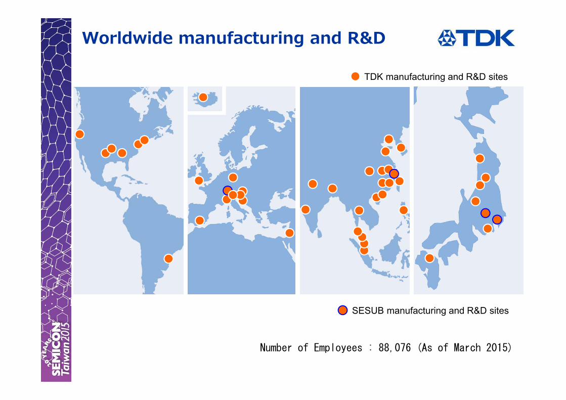
Worldwide manufacturing and R&D
TDK manufacturing and R&D sites
SESUB manufacturing and R&D sites
Number of Employees : 88,076 (As of March 2015)
SESUB Technology
Key Features of SESUBBenefit of Embedded PackageSESUB Process FlowDesign RuleSESUB application examples

SESUB
SESUB = Semiconductor Embedded in SUBstrate
Embedded IC
SESUB is TDK’s the state of the art substrate solution for SiPIC wafer is grinded to 50um and embedding in resin substrate and it enables total substrate thickness to be 300umSESUB is already proven technology by many customers and IC vendors
300um
Embedded IC
SESUB Cross Section
SESUB can be treated like typical PCB, SMT devices can mount on it.
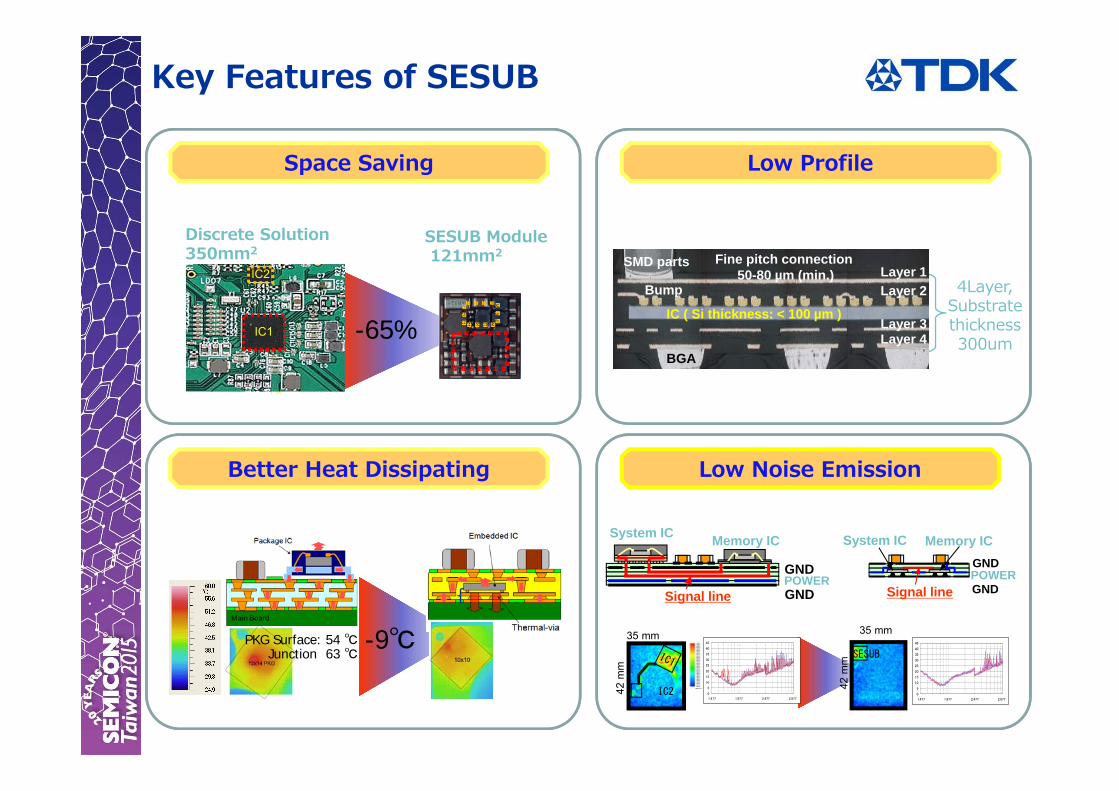
Key Features of SESUB
PKG Surface: 52 ℃Junction 54 ℃
4Layer,Substrate thickness300um
IC ( Si thickness: < 100 µm )
Bump
BGA
SMD parts Fine pitch connection50-80 µm (min.)
Layer 2Layer 1
Layer 4Layer 3
Low Profile
System IC Memory IC
Signal line
GND
GNDPOWER
GND
GNDPOWER
Signal line
System IC Memory IC
IC242 m
m35 mm
SESUB
42 m
m
35 mm
0
5
10
15
20
25
30
35
40
45
1.477 1.977 2.477 2.977
0
5
10
15
20
25
30
35
40
45
1.477 1.977 2.477 2.977
Low Noise Emission
PKG Surface: 54 ℃Junction 63 ℃
-9℃
Better Heat Dissipating
Space Saving
-65%
Discrete Solution 350mm2
SESUB Module121mm2
TWL6030
package7x
IC1
IC2

SESUB solutionDiscrete WLCSP Solution
Example of Space Saving
7.0x6.4mm= 45.0mm2
5.0x5.0mm= 25.0mm2
Embedded IC
WLCSP
Key Features of SESUB
Embedding IC saves PCB area almost half size compare to discrete solution.
Space Saving = 20mm2 (Compare with Discrete WLCSP solution)
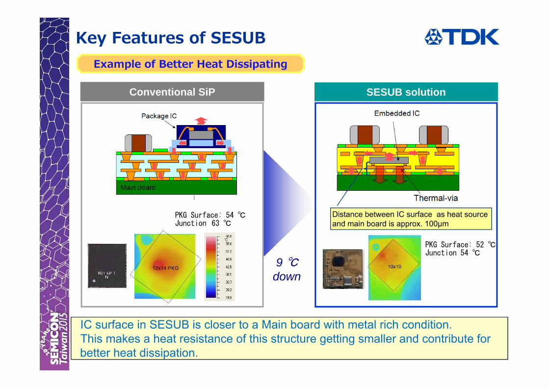
Distance between IC surface as heat source and main board is approx. 100μm
SESUB solutionConventional SiP
PKG Surface: 54 ℃Junction 63 ℃
PKG Surface: 52 ℃Junction 54 ℃
9 ℃down
IC surface in SESUB is closer to a Main board with metal rich condition. This makes a heat resistance of this structure getting smaller and contribute for better heat dissipation.
Example of Better Heat Dissipating
Key Features of SESUB
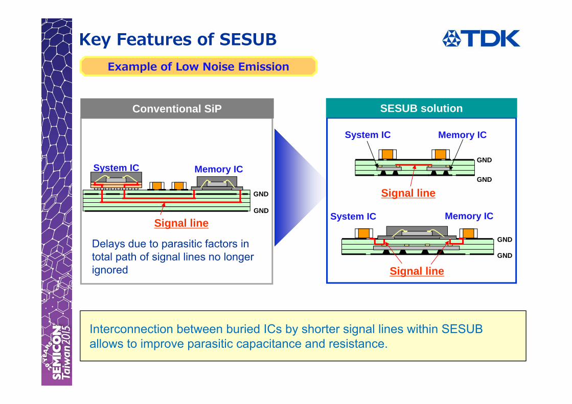
Signal line
Conventional SiP
System IC Memory IC
GND
GND
Interconnection between buried ICs by shorter signal lines within SESUB allows to improve parasitic capacitance and resistance.
Delays due to parasitic factors in total path of signal lines no longer ignored
GND
GND
Signal line
System IC Memory IC
SESUB solution
GND
GND
Signal line
System IC Memory IC
Example of Low Noise Emission
Key Features of SESUB
Discrete Solution
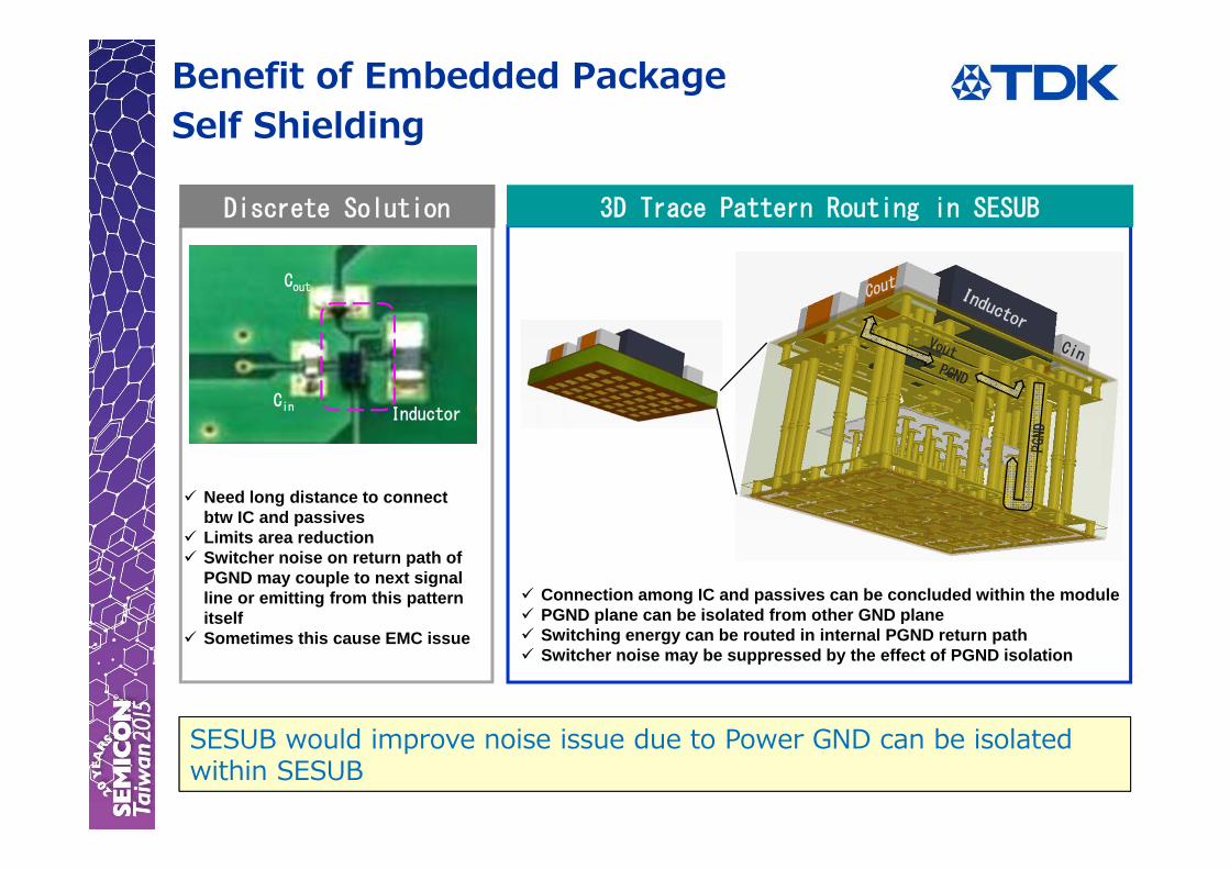
Benefit of Embedded PackageSelf Shielding
3D Trace Pattern Routing in SESUB
Need long distance to connect btw IC and passivesLimits area reductionSwitcher noise on return path of PGND may couple to next signal line or emitting from this pattern itselfSometimes this cause EMC issue
Connection among IC and passives can be concluded within the modulePGND plane can be isolated from other GND planeSwitching energy can be routed in internal PGND return pathSwitcher noise may be suppressed by the effect of PGND isolation
SESUB would improve noise issue due to Power GND can be isolated within SESUB
Inductor
Cout
Cin

Optimizing of switching loop (LC loop) by SESUB contributes suppressing of noise radiation
Max 69.9dBuV
Discrete Solution
Max 68.9dBuV SESUB Solution
Max 64.2dBuV
Max 76.0dBuV
Frequency (MHz)
(dB
uV)
Frequency (MHz)
(dB
uV)
(dB
uV)
Frequency (MHz)
Frequency (MHz)
(dB
uV)
Cin = 2.2uF (1005)Cout = 4.7uF (1005)Ind = 0.82uH (2012)
Cin = 2.2uF (1005)Cout = 4.7uF (1005)Ind = 0.82uH (2012)
fundamental of fsw
fundamental of fsw
Benefit of Embedded PackageSelf Shielding Effect
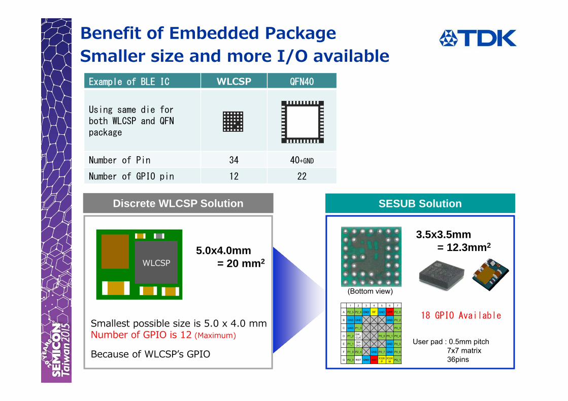
Example of BLE IC WLCSP QFN40
Using same die for both WLCSP and QFN package
Number of Pin 34 40+GND
Number of GPIO pin 12 22
Benefit of Embedded PackageSmaller size and more I/O available
SESUB SolutionDiscrete WLCSP Solution
1 2 3 4 5 6 7
A P2_5 P2_6 GND RF GND VPP P2_0
B GND GND GND P0_2
C GND P1_3 P0_3
D P1_2 SW_CLK P0_0 P0_1 P0_4
E P1_1 SWDIO GND P0_5
F P1_0 P2_4 GND P0_7 GND P0_6
G P2_3 RST GND VBATX32K
PX32K
M P2_1
User pad : 0.5mm pitch 7x7 matrix36pins
(Bottom view)
18 GPIO Available
3.5x3.5mm= 12.3mm25.0x4.0mm
= 20 mm2WLCSP
Smallest possible size is 5.0 x 4.0 mmNumber of GPIO is 12 (Maximum)
Because of WLCSPʼs GPIO

SESUB Features can be used for Next Gen Package SolutionSESUB Features can be used for Next Gen Package Solution
For PowerConnections
For signal connections
Flexible IC pad designOptimizing for better heat
releasing
Free access to IC pad positions within the die makes die size
optimized
Standard multi-VIA holes consume more space on IC
pad
SESUB can combine multi-VIA holes into one big hole and
contribute saving of IC pad space
Gaps between multiple Via holes required.
For obtaining same current flow capacityMaximum number die embedded
In MP : 2diesIn Development : 3dies
SESUB Copper Layer
IC Pad
SESUB enables new function IC in time to the market
Gap between dies : <500um
SESUB Package for Time in Market before making SoC
0.4m
m
Benefit of Embedded Package Can be Utilize unique technology of SESUB

IC direct connection
GND
Diode
Capacitor
Transisto
r
GND
Diode
Capacitor
Transisto
r
Wire Bonding: Peripheral Pad Arrangement
CSP:BGA Pad Arrangement
Utilizing Redistribution Layer
GND
Diode
Capacitor
Transisto
r
Direct Connection:Formed Pad on the Elements
• No need for redistribution layer: shorter lead times, high-speed, lower-cost,• Chip area reduction: miniaturization at lower cost• Performance improvement for RF and BB and high-speed memory applications• Thinner IC leads to low warpage
Actual: Requires RDL on the die for pinout No RDL for pinout
Benefit of Embedded Package

Complete Solution Provider
Design ICPreparation Embedding Assembly Tests
ICs Other comp.
Test proced.
Design Tools Passives Test
equip.Processes
Long experience and Know how in Module Business
Sales & logistic channels WW

SESUB Development & Production Locations
R&D Center
Production Location
R&D and Production Location
TDKApplication Design, Marketing
(Tokyo, Japan)
TDKSESUB Production, Process Development
(Kofu, Japan)
TDK-EPC (EPCOS)Marketing, Application Design
(Munich, Germany)
TDK-EPCAssembly, Test
(Wuxi, China)
SESUB Design Rule Roadmap
IC DieIC Die
S2L2 S1L1EIC GICSICV1/L1
V2/L2
TICBIC
BPIC
GPE
GVI
A
B
CD
Symbol
BPIC
A
L2/S2
L2
D
Embe
dded
Pad finishing
Multi layer
Encapsulation Metal cap
Bump capture pad
or Mold & Shieldor Mold
Fine
Lin
e
IC connection Diameter Unlimited max
Heat disipation
Occupation ratio 15 ~ 60 % ~ 70 %
Line and space
Via capture/landing pad
50 um
Pad Material
Outer:110/Inner:160um150 - 250 um 150 - 200 um
Pad location
Pad Pitch
2013 2014 2015 2016Item 2017
Both sideShingle side
Cu / Au / AlCu/Au
120 um
20/ 30 um34/ 46 um
Cu-OSP
30um
2 / 4 Layer4 Layer
Direct thamal via on IC back sideThin resin
80 um
10/ 20um

SESUB Application in the Market
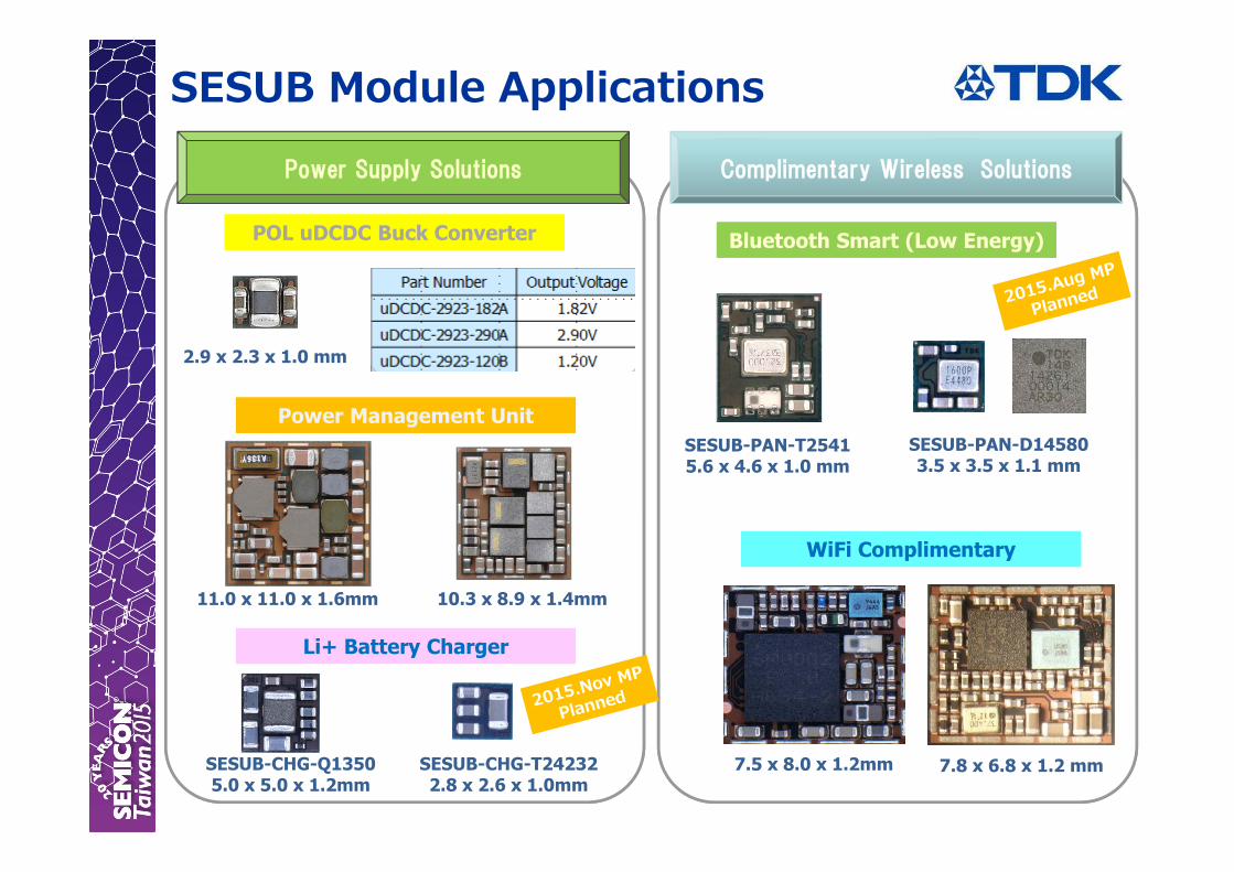
SESUB Module Applications
Power Management UnitPower Management Unit
11.0 x 11.0 x 1.6mm
2.9 x 2.3 x 1.0 mm
POL uDCDC Buck ConverterPOL uDCDC Buck Converter Bluetooth Smart (Low Energy)Bluetooth Smart (Low Energy)
SESUB-PAN-T25415.6 x 4.6 x 1.0 mm
WiFi ComplimentaryWiFi Complimentary
7.5 x 8.0 x 1.2mm 7.8 x 6.8 x 1.2 mm
Power Supply Solutions Complimentary Wireless Solutions
Li+ Battery ChargerLi+ Battery Charger
10.3 x 8.9 x 1.4mm
SESUB-PAN-D145803.5 x 3.5 x 1.1 mm
SESUB-CHG-T242322.8 x 2.6 x 1.0mm
SESUB-CHG-Q13505.0 x 5.0 x 1.2mm
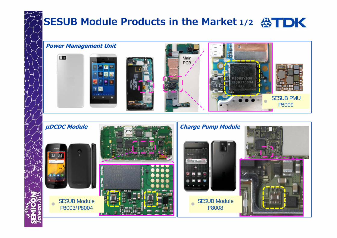
SESUB Module Products in the Market 1/2
Power Management Unit
μDCDC Module Charge Pump Module
SESUB PMUP8009
SESUB PMUP8009
SESUB Module P8008
SESUB Module P8008
SESUB ModuleP8003/P8004SESUB ModuleP8003/P8004
MainPCB
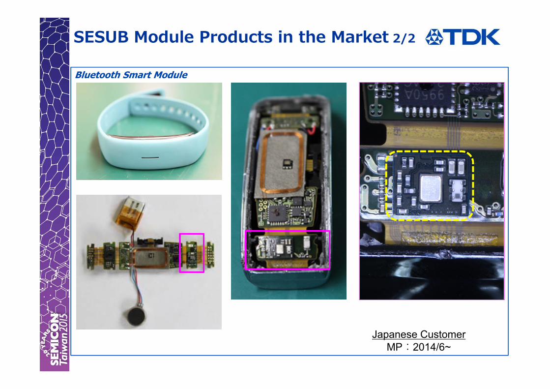
Bluetooth Smart Module
SESUB Module Products in the Market 2/2
Japanese Customer MP:2014/6~

Highly Integrated Power Management Unit
SESUB Solution for Mobile Application
Discrete + BGA packageSESUB PMU 1st Gen
-60%User Pad : 0.5mm pitch,20x21 Array, 381pads
TWL6030 package7x7mm
IC1
IC2
18.0 x 18.0mm = 320sq.mm 11.0 x 11.0mm = 121sq.mmMax height (inc. Shield) 1.63mm
SESUB PMU 2nd Gen
-24%
10.3 x 8.9mm = 91.67sq.mmMax height (inc. Shield) 1.43mm
User Pad : 0.4mm pitch,21x25 Array, 415pads

Advantage of the module solutionDialog Semiconductor DA14580, Bluetooth V4.1 Smart compliant is integratedTx power level : 0dBm, Rx Sensitivity level : -93dBmTx current consumption : 5mA, Rx current consumption : 5mAStandby current : 0.8uA
SESUB Solution for Wearable Application
Conventional Bluetooth Module
8.5
8.5
3.5
3.5
SESUB-PAN-D14580
Area Saving : 83%
Status: Sample is available, Mass Production starting from Aug 2015
SESUB-PAN-D14580 Bluetooth V4.1 Low Energy Module
Unit in mm

SESUB-CHG-T24232Li+ Battery Charger with TI BQ24232
SESUB Solution for Wearable Application
*excluding configuration resisters for battery charge conditions.Be flexible to various type of Li+ battery cells.
6.8
7.0
3.0 x 3.0IC size
Advantage of SESUB-CHG-T24232Saving PCB size (over 50%)Improving ASSY yield on application PCBPnP utilization for less PCB design work
Status: Engineering sample is available, MP start from Nov-2015
【Discrete circuit】PCB size : 47.6mm2
-79%
【TDK_Module】+ (4 x Resisters) PCB size : 9.8mm2
Unit in mm2.8
3.5

TDK-ASE Joint Venture
May 8th, 2015 Advanced Semiconductor Engineering, Inc. and TDK Corporation
announced that both companies will enter into an agreement to establish a joint venture company to manufacture IC embedded substrates using TDKʼs SESUB® technology.
Visit TDK Product Center on our web site for more detail.http://product.tdk.com/en/products/sesub/
Support Mail : [email protected]