Service Manual Full Panel Detachable High Power FM/AM...
44
Service Manual Full Panel Detachable High Power FM/AM Stereo Receiver Compact Disc Player FXD-680GD 114782877 FXD-685GD 114782878 SEL FM/MW/LW CD RECEIVER 45W x 4 CD-R&RW FXD-680GD SEL FM/MW/LW CD RECEIVER 45W x 4 CD-R&RW FXD-685GD Contents SERVICE NOTE AND PRECATIONS............................................................................................................................................................................... 2 OPERATION CHECK ....................................................................................................................................................................................................... 5 ALIGNMENT LOCATIONS................................................................................................................................................................................................ 6 ELECTRICAL ADJUSTMENTS......................................................................................................................................................................................... 7 BLOCK DIAGRAM .......................................................................................................................................................................................................... 18 IC/TRANSISTOR LEAD IDENTIFICATION..................................................................................................................................................................... 20 CD MECHANISM EXPLODED VIEW ............................................................................................................................................................................. 21 CABINET & CHASSIS EXPLODED VIEW ...................................................................................................................................................................... 22 PART LIST – CD MECHANISM ...................................................................................................................................................................................... 23 PART LIST CABINET, CHASS AND ACCESSORY ....................................................................................................................................................... 25 PART LIST MAIN ............................................................................................................................................................................................................ 27 PART LIST KEY.............................................................................................................................................................................................................. 30 PART LIST CD SERVO .................................................................................................................................................................................................. 31 PART LIST REMOTE...................................................................................................................................................................................................... 33 PART LIST JB/GIB.......................................................................................................................................................................................................... 34 SCHEMATIC DIAGRAM ................................................................................................................................................................................................. 35 CIRCUIT BOARD DIAGRAM .......................................................................................................................................................................................... 39 REFERENCE No. SM-0600003 FILE NO.
Transcript of Service Manual Full Panel Detachable High Power FM/AM...

Service Manual Full Panel Detachable High Power FM/AM Stereo Receiver Compact Disc Player
FXD-680GD 114782877 FXD-685GD 114782878
SEL
FM/MW/LW CD RECEIVER 45W x 4 CD-R&RW
FXD-680GD
SEL
FM/MW/LW CD RECEIVER 45W x 4 CD-R&RW
FXD-685GD
Contents SERVICE NOTE AND PRECATIONS............................................................................................................................................................................... 2
OPERATION CHECK ....................................................................................................................................................................................................... 5
ALIGNMENT LOCATIONS................................................................................................................................................................................................ 6
ELECTRICAL ADJUSTMENTS......................................................................................................................................................................................... 7
BLOCK DIAGRAM .......................................................................................................................................................................................................... 18
IC/TRANSISTOR LEAD IDENTIFICATION..................................................................................................................................................................... 20
CD MECHANISM EXPLODED VIEW ............................................................................................................................................................................. 21
CABINET & CHASSIS EXPLODED VIEW...................................................................................................................................................................... 22
PART LIST – CD MECHANISM...................................................................................................................................................................................... 23
PART LIST CABINET, CHASS AND ACCESSORY ....................................................................................................................................................... 25
PART LIST MAIN............................................................................................................................................................................................................ 27
PART LIST KEY.............................................................................................................................................................................................................. 30
PART LIST CD SERVO .................................................................................................................................................................................................. 31
PART LIST REMOTE...................................................................................................................................................................................................... 33
PART LIST JB/GIB.......................................................................................................................................................................................................... 34
SCHEMATIC DIAGRAM ................................................................................................................................................................................................. 35
CIRCUIT BOARD DIAGRAM .......................................................................................................................................................................................... 39
REFERENCE No. SM-0600003
FILE NO.

1
SPECIFICATIONS FM TUNER Frequency Range ......................................................................................FM 87.5 - 108.0 MHz (50 KHz Step)
Sensitivity.......................................................................................................................... FM 3 µV (S/N=30 dB)
Stereo Separating (FM) ..............................................................................................................30 dB (at 1kHz)
Signal to noise ratio (FM).........................................................................................................Better than 50 dB
AM TUNER
Frequency Range ..........................................................................................MW 522 - 1620 kHz (9 KHz Step)
Sensitivity.....................................................................................................................MW 32 dBµ (S/N=20 dB) Signal to Noise Radio ............................................................................................................... More than 45 dB
LW TUNER Frequency Range ...................................................................................................................LW 144 - 288 kHz
Sensitivity......................................................................................................................LW 35 dBµ (S/N=20 dB)
CD PLAYER Frequency Response................................................................................................................20Hz - 20,000Hz
Signal to Noise Radio ............................................................................................................... More than 65 dB
Channel Separation .................................................................................................................. More than 60 dB
T. H. D.......................................................................................................................................Less than 0.30%
AUDIO AMPLIFIER & GENERAL Output Power........................................................................................................................................4 X 45 W
Speaker Output Impedance.......................................................................................................................4 ohm
Power Source ........................................................................................................... DC 12V, Negative ground.
Specifications are subject to change without notice.
2
SERVICE NOTES AND PRECAUTIONS: Service notes: 1. Make sure that the power lead is connected properly to
Power source, otherwise damage to radio may result. If a
Battery, eliminator is used as a power source in place of a
Battery, it must be filtered and regulated. (The power sup-
ply capacity should be more than 5 amps).
2. Integrated circuits (ICs) are used in this unit. Because the
ICs are direct-coupled devices, as to all electronic equip-
ment, reading within 10% of the indicated values are acc-
eptable. Allowance must also be made for variations in
supply voltage. It is expected that any breakdown within
the IC results in drastic changes of the operating voltages
at the terminals.
3. When replacing a power output IC, remember to use the
IC specified in the parts list; Coat the IC-fin with silicon grease.
WARNING In using meters, signal generator and any tool in servicing
ICs, extreme care is needed.
DO NOT SHORT THE IC TERMINALS TO THE PATTERN ON THE PC BOARD OR TO EACH OTHER. THE IC WILL BE INSTANTANEOUSLY DESTROYED. Adjustment procedure: Alignment is performed at factory with laboratory equipment.
Therefore, before alignment is attempted, the unit should be
thoroughly checked for circuit troubles.
Notes: 1. Check for specified source voltage-DC, 14.4 volts.
2. Connect an AC voltmeter (AC VM) across speaker or
dummy load (4 ohms. 20W, wire wound resistor)….see
fig. 1-3. (ELECTRICAL ADJUSTMENTS).
3. Signal input must be kept as low as possible to avoid
overload and clipping (use highest sensitivity of output
indicator).
4. Repeat adjustment to ensure good results.
5. Non-metallic alignment tools, must be used (especially
at FM alignment).
6. for alignment location details, refer to CIRCUIT BOARD
PARTS LOCATIONS
Installation procedure: 1. To prevent a short circuit, remove the key from the ignition
and disconnect the battery. 2. Make the proper input and output wire connections for
each unit. 3. Connect the wiring harness wires in the following order:
ground, sealers, battery, ignition. 4. Connect the wiring harness connector to the unit. 5. Install the unit in your car. 6. Reconnect the battery. 7. Disentails by reversing the installation procedure.
CAUTION The rear-panel which also heat sink is very hot. Don’t
burn!! If your car’s ignition does not have an ACC position,
connect the ignition wires to a power source that can be turned on and off with the ignition key. If you connect the ignition wire to a power source with a connect voltage supply, as with battery wire the battery may die.
If the console has a lid, make sure to install the unit so that the cover will not hit the lid when closing and open- ing.
If the fuse blows, first make sure the wires aren’t touch- ing to case a short circuit, then replace the old fuse with one with the same rating.
Do not let unconnected wires or terminals touch metal on the car or anything else conducting electricity. To prevent a short circuit, do not remove the caps on the ends of the unconnected wires or the terminals.
Connect the speaker wires correctly to the terminals to which they correspond. The unit may be damaged or fair to work if you share the wires or ground them to any metal part in the car.
After the unit is installed, check whether the brake lamps, blinkers, wipers, etc. On the car are working properly.
Insulate unconnected wires vinyl tape or other similar material.
3
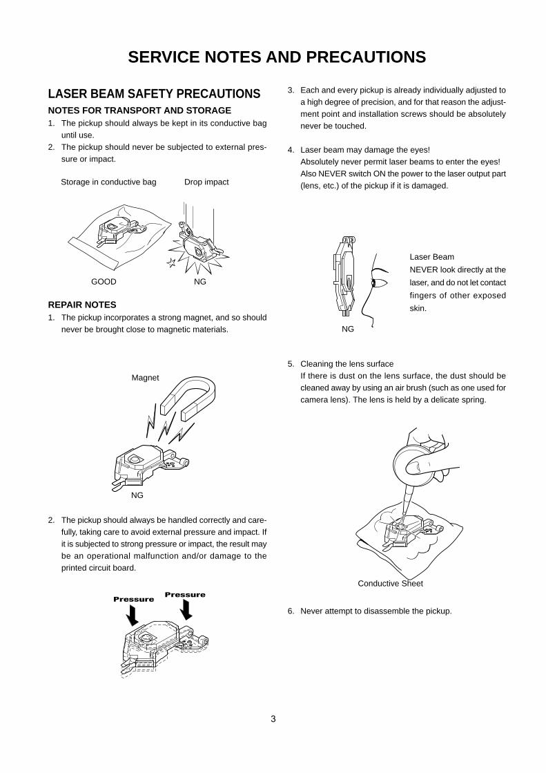
SERVICE NOTES AND PRECAUTIONS
LASER BEAM SAFETY PRECAUTIONSNOTES FOR TRANSPORT AND STORAGE1. The pickup should always be kept in its conductive bag
until use.2. The pickup should never be subjected to external pres-
sure or impact.
REPAIR NOTES1. The pickup incorporates a strong magnet, and so should
never be brought close to magnetic materials.
NG
Magnet
NG
2. The pickup should always be handled correctly and care-fully, taking care to avoid external pressure and impact. Ifit is subjected to strong pressure or impact, the result maybe an operational malfunction and/or damage to theprinted circuit board.
3. Each and every pickup is already individually adjusted toa high degree of precision, and for that reason the adjust-ment point and installation screws should be absolutelynever be touched.
4. Laser beam may damage the eyes!Absolutely never permit laser beams to enter the eyes!Also NEVER switch ON the power to the laser output part(lens, etc.) of the pickup if it is damaged.
Laser Beam
NEVER look directly at the
laser, and do not let contact
fingers of other exposed
skin.
NG
5. Cleaning the lens surfaceIf there is dust on the lens surface, the dust should becleaned away by using an air brush (such as one used forcamera lens). The lens is held by a delicate spring.
Conductive Sheet
6. Never attempt to disassemble the pickup.
Storage in conductive bag Drop impact
GOOD
PressurePressure
4
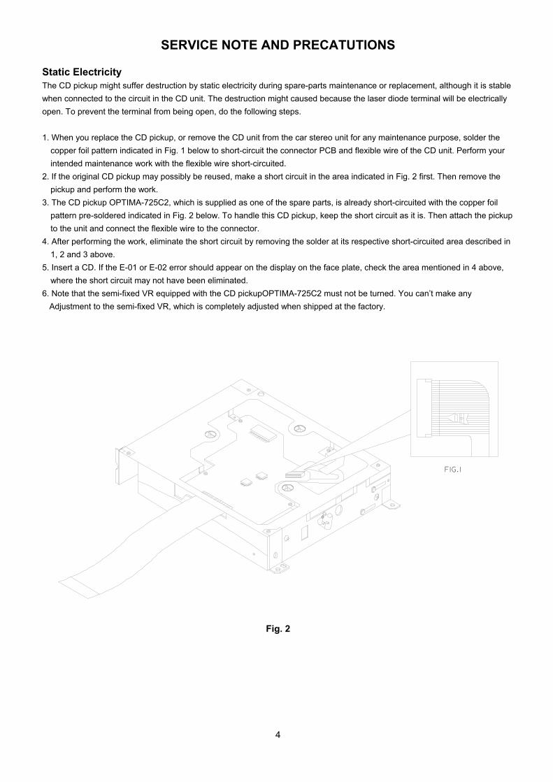
SERVICE NOTE AND PRECATUTIONS Static Electricity The CD pickup might suffer destruction by static electricity during spare-parts maintenance or replacement, although it is stable when connected to the circuit in the CD unit. The destruction might caused because the laser diode terminal will be electrically open. To prevent the terminal from being open, do the following steps. 1. When you replace the CD pickup, or remove the CD unit from the car stereo unit for any maintenance purpose, solder the
copper foil pattern indicated in Fig. 1 below to short-circuit the connector PCB and flexible wire of the CD unit. Perform your intended maintenance work with the flexible wire short-circuited.
2. If the original CD pickup may possibly be reused, make a short circuit in the area indicated in Fig. 2 first. Then remove the pickup and perform the work.
3. The CD pickup OPTIMA-725C2, which is supplied as one of the spare parts, is already short-circuited with the copper foil pattern pre-soldered indicated in Fig. 2 below. To handle this CD pickup, keep the short circuit as it is. Then attach the pickup to the unit and connect the flexible wire to the connector.
4. After performing the work, eliminate the short circuit by removing the solder at its respective short-circuited area described in 1, 2 and 3 above.
5. Insert a CD. If the E-01 or E-02 error should appear on the display on the face plate, check the area mentioned in 4 above, where the short circuit may not have been eliminated.
6. Note that the semi-fixed VR equipped with the CD pickupOPTIMA-725C2 must not be turned. You can’t make any Adjustment to the semi-fixed VR, which is completely adjusted when shipped at the factory.
FIG.1
Fig. 2
5
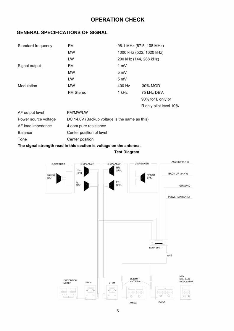
OPERATION CHECK GENERAL SPECIFICATIONS OF SIGNAL Standard frequency
Signal output
Modulation
FM
MW
LW
FM
MW
LW
MW
FM Stereo
98.1 MHz (87.5, 108 MHz)
1000 kHz (522, 1620 kHz)
200 kHz (144, 288 kHz)
1 mV
5 mV
5 mV
400 Hz 30% MOD.
1 kHz 75 kHz DEV.
90% for L only or
R only pilot level 10% AF output level FM/MW/LW
Power source voltage DC 14.0V (Backup voltage is the same as this)
AF load impedance 4 ohm pure resistance
Balance Center position of level
Tone Center position The signal strength read in this section is voltage on the antenna.
Test Diagram
FL.SPK.
FR.SPE.
BACK UP (14.4V)
GROUND
POWER ANTANNA
MPXSTEREOSMODULATOR
FM SGAM SG
DUMMYANTANNA
VTVMVTVMDISTORTIONMETER
ACC (DV14.4V)
SPK.RR.
SPR.RL.
MAIN UNIT
4−SPEAKER 4−SPEAKER 2−SPEAKER
FRONT SPK.SPK.
FRONT
2−SPEAKER
ANT
6
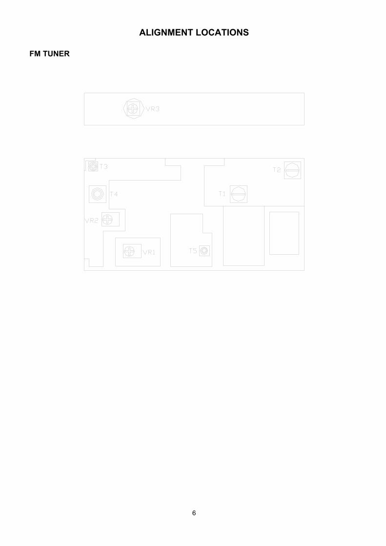
ALIGNMENT LOCATIONS FM TUNER

7
ALIGNMENT PROCEDURES FM ADJUSTMENT Equipment Required
AM IF/RF signal generator Solid-state voltmeter (SSVM) Regulated DC power supply 2-CH voltmeter Distortion meter
FM Alignment Using FM Signal Generator Note: Press the radio power switch to on the radio. Signal generator output must be kept as low as possible
to avoid overload and clipping.
Step Generator Coupling
Generator Display Setting
Adjustment Remarks
Stereo Separation
Signal Generator to antenna receptacle
98.1 MHz Int. 1 kHz Dev. 75 kHz L+R = 90 % pilot = 10 %
98.1 MHz
VR1
Adjust AF output power at maximum separating more than 30 dB
FM SNC Adjustment
98.1 MHz Dev. 75 kHz L+R=90 % Int. 1 kHz 60dBµV output
98.1 MHz @ 40 dBµ
98.1 MHz
VR2
Stereo Separation 25 dB (±5 dB)
STOP SENS.
Signal Generator to antenna receptacle
98.1 MHz Mod. 1kHz Dev 75kHz
98.1 MHz
VR3
Adjust AF to stop station.
Note: The tuner module is well-adjust and adjustment is not recommended.

8
RADIO OPERATION FOR FXD-680GD, FXD685GD
SEL
FM/MW/LW CD RECEIVER 45W x 4 CD-R&RW
27 6
85 4 31 FXD-680GD
SEL
FM/MW/LW CD RECEIVER 45W x 4 CD-R&RW
27 6
85 4 31
FXD-685GD
SWITCHING TO RADIO MODE…………………….…1 Press SOURCE button 1 to select radio mode, the radio mode appears in the display together with the memory band and frequency.
SELECTING THE FREQUENCY BAND……………..2 At radio mode, press BAND/LOUD button 2 shortly to select the desired band. The reception band will change in the following order: FM1 FM2 FM3 MW LW
RADIO TUNING…………………………………………3 Press the TUN/TRK or button 3 shortly to activate automatic seek function. Press for several seconds
until “MANUAL” appears on the display, the manual tuning mode is selected. If both buttons have not pressed for
several seconds, it will revert to seek tuning mode and “AUTO” appeared on the display.
AUTOMATIC MEMORY STORING & PROGRAM SCANNING…………………4 - Automatic memory storing
Press P.SCAN/AST button 4 for several seconds, the radio searches for 6 strongest stations and stores them into the presets of the currently selected band.
- Program scanning Press P.SCAN/AST button 4 shortly to scan preset station. When the field strength level is more than the threshold level of stop level, the radio is holding at that preset number for several seconds with release mute, then searches again.
STORING PRESET STATIONS .................................5 The preset buttons 5 can be used to store 6 stations in each band (FM 1, FM 2, FM 3 and MW, LW) for convenient
access to your favorite stations.
9
• Programming stations ..... 1. Select the desired band, then tune in the station you want to store in memory.
2. Press and hold one of the preset buttons 5 for more than 2 seconds until the
corresponding preset button number appears. Repeat steps 1. and 2. to program
additional stations.
• Quick tuning .................….... Select the desired band, then press one of the six preset buttons 5.
LOCAL/DISTANT SELECTION ...........................…..6 Press LOC button 6 to set local or distant stations.
Use local position (LOCAL/LOC appears on the display) for reception of strong station, and distant position (DX
appears on the display) for reception of weaker stations. This function is effective during AUTO SEEK operation.
MONO/STEREO SELECTION .......................….…...7 Press MONO button 7 to select mono or stereo mode. You can sometimes improve reception of distant stations by selecting mono operation.
FREQUENCY SCAN OPERATION.......................….8 Press F.SCAN button 8 to set the function to frequency scan mode, which scans stations and stop for several seconds at each receivable signal. Press F.SCAN button again to stop scanning.

10
CD OPERATION FOR FXD-680GD, FXD-685GD
SEL
FM/MW/LW CD RECEIVER 45W x 4 CD-R&RW
34 5 6 7
8
2
1
FXD-680GD
SEL
FM/MW/LW CD RECEIVER 45W x 4 CD-R&RW
34 5 6 7
8
2
1
FXD-685GD
LOADING AND EJECTING THE CD………………1,8 Insert a disc into the CD slot 1 and the CD player will start.
The system remains in CD mode and “ ” appears in the display.
Press the eject button 8 to eject a disc.
SWITCHING TO CD MODE.......................................2 Press the SOURCE button 2 with the power on to switch from radio mode or AUX mode to CD mode.
When the CD mode is switched on while a disc is loaded, play resumes from the point at which play was stopped.
When the entire disc has played, the unit returns to the first track and play resumes. SKIPPING TRACKS .............................................…3 Press the TUN/TRK button to skip to the beginning of the next track.
Press the TUN/TRK button to skip to the beginning of the previous track.
Press and hold the TUN/TRK or TUN/TRK button 3 for several seconds to search quickly (with sound) in
the forward or reverse direction.
When the button is released, the CD resumes normal play.
Notes:
PLACING THE CD IN PAUSE MODE ......................4 While playing a CD, press the PAU button 4.
To resume playing, press the PAU button 4 again.
• You can play CD-Rs or CD-RWs (rewritable CDs) on this unit in proper condition.
• Some CD-Rs/CD-RWs (depending on the equipment used for its recording or the
condition of the disc) may not play on this unit.
• You cannot play CD-R/CD-RW that is not finalized. (A finalize process necessary for a

11
Notes REPEAT MODE ........................................................... 6 Press the RPT button 6 to play the current track repeatedly.
To cancel this mode, press the RPT button 6 again. SHUFFLE MODE.......................................................... 7 This function plays the tracks on a CD in random order.
Press the SHF button 7 to begin shuffle play.
To cancel this mode, press the SHF button 7 again.
SCAN MODE (PLAYING THE BEGINNING OF EACH TRACK) ....................................................... 5 This function plays the first several seconds of each track sequentially.
Press the SCN button 5 to begin the scan mode.
To cancel this mode, press the SCN button 5 again.
• During playback of a CD, the CD running indicator spins.
• The unit will turn-on automatically when a CD is inserted if the ignition switch is “ON”.

12
AUX MODE OPERATION FOR FXD-680GD
SEL
FM/MW/LW CD RECEIVER 45W x 4 CD-R&RW
1 SWITCHING TO AUX MODE.......................................1 The unit has a pair of auxiliary input terminals (see WIRING figure on page 18). This allows you to listen to an
auxiliary audio source (MP3, portable cassette player, etc).
Press the SOURCE button 1 with the power on to switch from radio mode or CD mode to AUX mode.
13
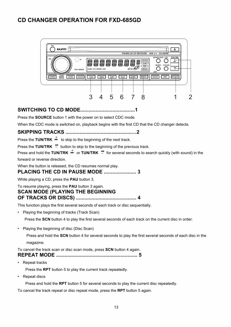
CD CHANGER OPERATION FOR FXD-685GD
SEL
FM/MW/LW CD RECEIVER 45W x 4 CD-R&RW
23 4 5 6 7 8 1
SWITCHING TO CD MODE.......................................1 Press the SOURCE button 1 with the power on to select CDC mode.
When the CDC mode is switched on, playback begins with the first CD that the CD changer detects.
SKIPPING TRACKS ...............................................…2 Press the TUN/TRK to skip to the beginning of the next track.
Press the TUN/TRK button to skip to the beginning of the previous track. Press and hold the TUN/TRK or TUN/TRK for several seconds to search quickly (with sound) in the
forward or reverse direction.
When the button is released, the CD resumes normal play. PLACING THE CD IN PAUSE MODE ....................... 3 While playing a CD, press the PAU button 3.
To resume playing, press the PAU button 3 again. SCAN MODE (PLAYING THE BEGINNING OF TRACKS OR DISCS) ........................................... 4 This function plays the first several seconds of each track or disc sequentially.
• Playing the beginning of tracks (Track Scan)
Press the SCN button 4 to play the first several seconds of each track on the current disc in order.
• Playing the beginning of disc (Disc Scan)
Press and hold the SCN button 4 for several seconds to play the first several seconds of each disc in the
magazine.
To cancel the track scan or disc scan mode, press SCN button 4 again. REPEAT MODE .......................................................... 5 • Repeat tracks
Press the RPT button 5 to play the current track repeatedly.
• Repeat discs
Press and hold the RPT button 5 for several seconds to play the current disc repeatedly.
To cancel the track repeat or disc repeat mode, press the RPT button 5 again.
14
SHUFFLE MODE......................................................... 6 This function plays the tracks on one CD or all CDs in the magazine in random order.
• “Shuffle-playing” tracks
Press the SHF button 6 to play the current disc in random order.
• “Shuffle-playing” discs
Press and hold the SHF button 6 for several seconds. The system selects a disc at random and plays all tracks
on that disc. When all tracks have been played, the next disc is selected and “Shuffle-playing” is repeated.
To cancel the track shuffle or disc shuffle mode, press the SHF button 6 again.
SELECTING A DISC................................................ 7,8 Press the DISC – button 7 to select the preceding disc.
Press the DISC + button 8 to select the next disc.
Note
• Use with only SANYO CD Changer.

15
REMOTE CONTROL (OPTIONAL) FOR FXD-680GD, FXD-685GD
POWER VOL
TUN/TRK
VOLLOUD AST
PAU SCN RPT
SHF
1
5 3
649
10
15
13
2
7
8111412
1.POWER
2. AUDIO 3. VOL 4. VOL 5. SOURCE 6. TUN/TRK 7. TUN/TRK
9. BAND/LOUD
10.PAU
11.SCN
12.RPT
13.SHF
14.SOUND
15.1~6 Preset buttons

16
HINTS FOR PROPER AND SAFE OPERATION • Condensation
Moisture can condense on the optical lens of the CD player during humid or rainy days, or after the car heater is
turned on. If this occurs the disc player may not function properly. To remedy the situation, remove the disc from
the unit and wait approximately one hour. This should allow the moisture to evaporate and restore normal
operation.
• Temperature Consideration
The unit may not operate correctly in extremely hot or cold temperatures. Avoid exposing the unit to extremely
high or low temperatures.
• Interruptions in the sound (skipping)
When the car is driven on very rough surfaces, the sound from the CD player may skip and be interrupted. This
will not cause any damage to the disc or the player. If this occurs, wait for the road surface to improve before
using the CD player.
• Safety
For safer driving, keep the volume at a moderate level to enable you to hear outside sounds (such as
emergency vehicle sirens).
• Cleaning the unit
Clean the unit with a soft, dry cloth. Stains should be removed by wiping the surfaces with a soft cloth immersed
in lukewarm water and wrung dry. Never use strong chemicals or solvents. These will damage the finish of the
unit.
• Disc care
When not using the disc player for extended periods, remove the compact disc and return it to the plastic
storage case. Do not leave a disc partially ejected from the player. If an ejected disc remains in the loading slot
for approximately 10 seconds, the player will reload the disc to prevent damage.
• Servicing Should a problem develop, do not open the unit or try to repair it yourself. If servicing is required, bring the unit to a Sanyo Authorized Service Center.

17
ELECTRICAL ADJUSTMENTS
DUMMY BOX SCHEMATIC
AM DUMMY ANTENNA
FM DUMMY ANTENNA

18
BLOCK DIAGRAM FOR FXD-680GD

19
BLOCK DIAGRAM FOR FXD-685GD
20
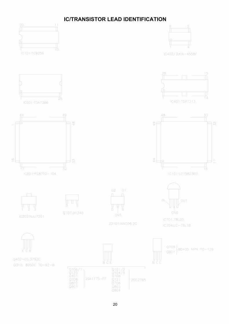
IC/TRANSISTOR LEAD IDENTIFICATION
21
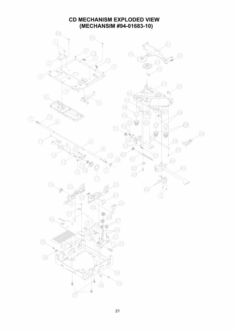
CD MECHANISM EXPLODED VIEW (MECHANSIM #94-01683-10)
22
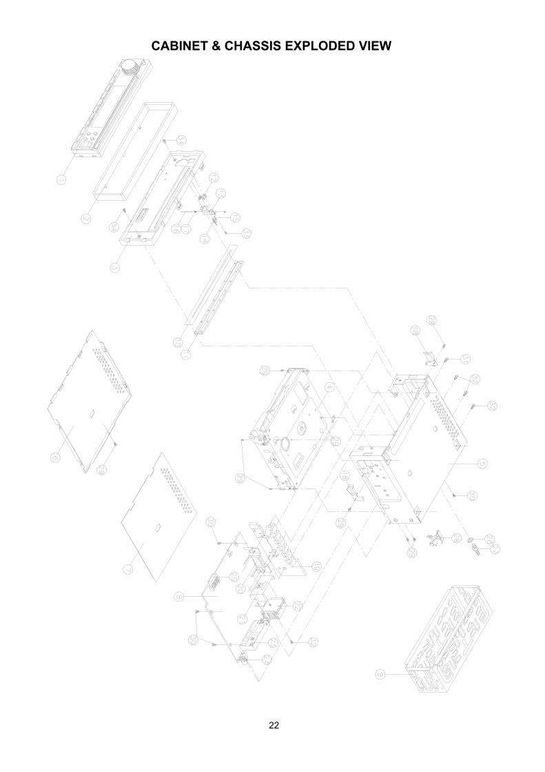
CABINET & CHASSIS EXPLODED VIEW
23
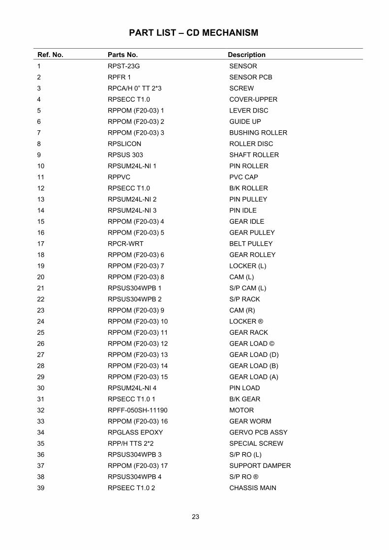
PART LIST – CD MECHANISM
Ref. No. Parts No. Description 1
2
3
4
5
6
7
8
9
10
11
12
13
14
15
16
17
18
19
20
21
22
23
24
25
26
27
28
29
30
31
32
33
34
35
36
37
38
39
RPST-23G
RPFR 1
RPCA/H 0” TT 2*3
RPSECC T1.0
RPPOM (F20-03) 1
RPPOM (F20-03) 2
RPPOM (F20-03) 3
RPSLICON
RPSUS 303
RPSUM24L-NI 1
RPPVC
RPSECC T1.0
RPSUM24L-NI 2
RPSUM24L-NI 3
RPPOM (F20-03) 4
RPPOM (F20-03) 5
RPCR-WRT
RPPOM (F20-03) 6
RPPOM (F20-03) 7
RPPOM (F20-03) 8
RPSUS304WPB 1
RPSUS304WPB 2
RPPOM (F20-03) 9
RPPOM (F20-03) 10
RPPOM (F20-03) 11
RPPOM (F20-03) 12
RPPOM (F20-03) 13
RPPOM (F20-03) 14
RPPOM (F20-03) 15
RPSUM24L-NI 4
RPSECC T1.0 1
RPFF-050SH-11190
RPPOM (F20-03) 16
RPGLASS EPOXY
RPP/H TTS 2*2
RPSUS304WPB 3
RPPOM (F20-03) 17
RPSUS304WPB 4
RPSEEC T1.0 2
SENSOR
SENSOR PCB
SCREW
COVER-UPPER
LEVER DISC
GUIDE UP
BUSHING ROLLER
ROLLER DISC
SHAFT ROLLER
PIN ROLLER
PVC CAP
B/K ROLLER
PIN PULLEY
PIN IDLE
GEAR IDLE
GEAR PULLEY
BELT PULLEY
GEAR ROLLEY
LOCKER (L)
CAM (L)
S/P CAM (L)
S/P RACK
CAM (R)
LOCKER ®
GEAR RACK
GEAR LOAD ©
GEAR LOAD (D)
GEAR LOAD (B)
GEAR LOAD (A)
PIN LOAD
B/K GEAR
MOTOR
GEAR WORM
GERVO PCB ASSY
SPECIAL SCREW
S/P RO (L)
SUPPORT DAMPER
S/P RO ®
CHASSIS MAIN
24
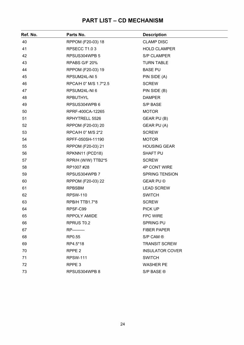
PART LIST – CD MECHANISM
Ref. No. Parts No. Description 40
41
42
43
44
45
46
47
48
49
50
51
52
53
54
55
56
57
58
59
60
61
62
63
64
65
66
67
68
69
70
71
72
73
RPPOM (F20-03) 18
RPSECC T1.0 3
RPSUS304WPB 5
RPABS G/F 20%
RPPOM (F20-03) 19
RPSUM24L-NI 5
RPCA/H 0” M/S 1.7*2.5
RPSUM24L-NI 6
RPBUTHYL
RPSUS304WPB 6
RPRF-400CA-12265
RPHYTRELL 5526
RPPOM (F20-03) 20
RPCA/H 0” M/S 2*2
RPFF-050SH-11190
RPPOM (F20-03) 21
RPKNN11 (PCD18)
RPR/H (W/W) TTB2*5
RP1007 #28
RPSUS304WPB 7
RPPOM (F20-03) 22
RPBSBM
RPSW-110
RPB/H TTB1.7*8
RPSF-C99
RPPOLY AMIDE
RPRUS T0.2
RP---------
RP0.55
RP4.5*18
RPPE 2
RPSW-111
RPPE 3
RPSUS304WPB 8
CLAMP DISC
HOLD CLAMPER
S/P CLAMPER
TURN TABLE
BASE PU
PIN SIDE (A)
SCREW
PIN SIDE (B)
DAMPER
S/P BASE
MOTOR
GEAR PU (B)
GEAR PU (A)
SCREW
MOTOR
HOUSING GEAR
SHAFT PU
SCREW
4P CONT WIRE
SPRING TENSION
GEAR PU ©
LEAD SCREW
SWITCH
SCREW
PICK UP
FPC WIRE
SPRING PU
FIBER PAPER
S/P CAM ®
TRANSIT SCREW
INSULATOR COVER
SWITCH
WASHER PE
S/P BASE ®

25
PART LIST CABINET & CHASSIS
Ref. No. Part No. Description 1
2
3
4
5
6
7
8
9
10
11
12
13
14
15
16
17
18
19
20
21
22
23
24
25
26
27
28
29
30
31
32
33
34
RP51-V3626-80B
RP51-V3620-00
RP94-01683-10
RP61-V3601-00
RP61-V3604-00
RP35-V3601-00
RP11-17021-025
RP61-3603-00
RP81-68608-01
RP43-16301-00
RP52-V3636-00
RP39-V3611-00
RP52-V3637-00
RP36-V3606-00
RP34-16307-00
RP36-A1701-00
RP39-V3608-00
RP39-V3604-00
RP39-V3607-00
RP39-V3603-01
RP25-16638-36D
RP29-00347-02
RP39-K6614-00
RP25-F1476-00
RP35-50001-00
RP40-05018-04
RP52-V3651-00
RP40-02604-01
RP40-02606-01
RP40-02608-01
RP40-02610-01
RP40-120080-21
RP40-12606-01
Panel
Trim Ring (S. OPC1202)
Base (For CD)
CD MECHA. CDM-1683 EUR (143A W/O PCB)
Main Bracket (CD)
Bottom Cover
Main Fiber
Main Board
Mounting Box
Shade (II)
PC Plate - CD
Hook Plate
FIX Bracket For Slide
Lock Plate
Spring - Locked 0.35
Shaft
Locker Spring (Ø0.70)
Lock Spring
Heat Sink (4)
IC Bracket
Socket Bracket (1.0) (For CD1702)
36PIN ISO Socket (No CDC/RCA)
MITSVMI Tuner FAE-347-A29
Antenna Socket
15PIN SKT R41/1476A (KENWOOD)
Spring Nut M5
Screw Ø5X18 HH
Antenna Holder
Screw Ø2.6 X 4 BH/MS
Screw Ø2.6 X 6 BH/MS
Screw Ø2.6 X 8 BH/MS
Screw Ø2.6 X 10 BH/MS
Screw Ø2 X 8 BA/ST Black
Screw Ø2.6 X 6 BH/MS Black
26
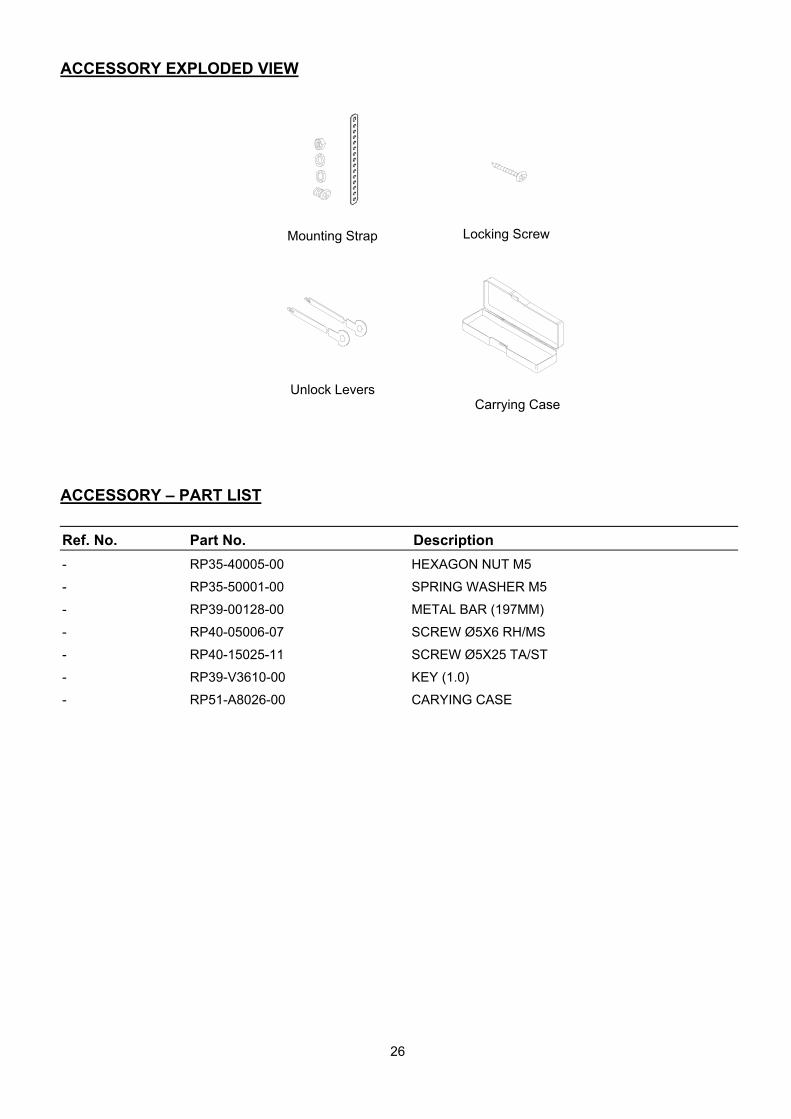
ACCESSORY EXPLODED VIEW
ACCESSORY – PART LIST
Ref. No. Part No. Description -
-
-
-
-
-
-
RP35-40005-00
RP35-50001-00
RP39-00128-00
RP40-05006-07
RP40-15025-11
RP39-V3610-00
RP51-A8026-00
HEXAGON NUT M5
SPRING WASHER M5
METAL BAR (197MM)
SCREW Ø5X6 RH/MS
SCREW Ø5X25 TA/ST
KEY (1.0) CARYING CASE
Mounting Strap Locking Screw
Unlock Levers Carrying Case
27
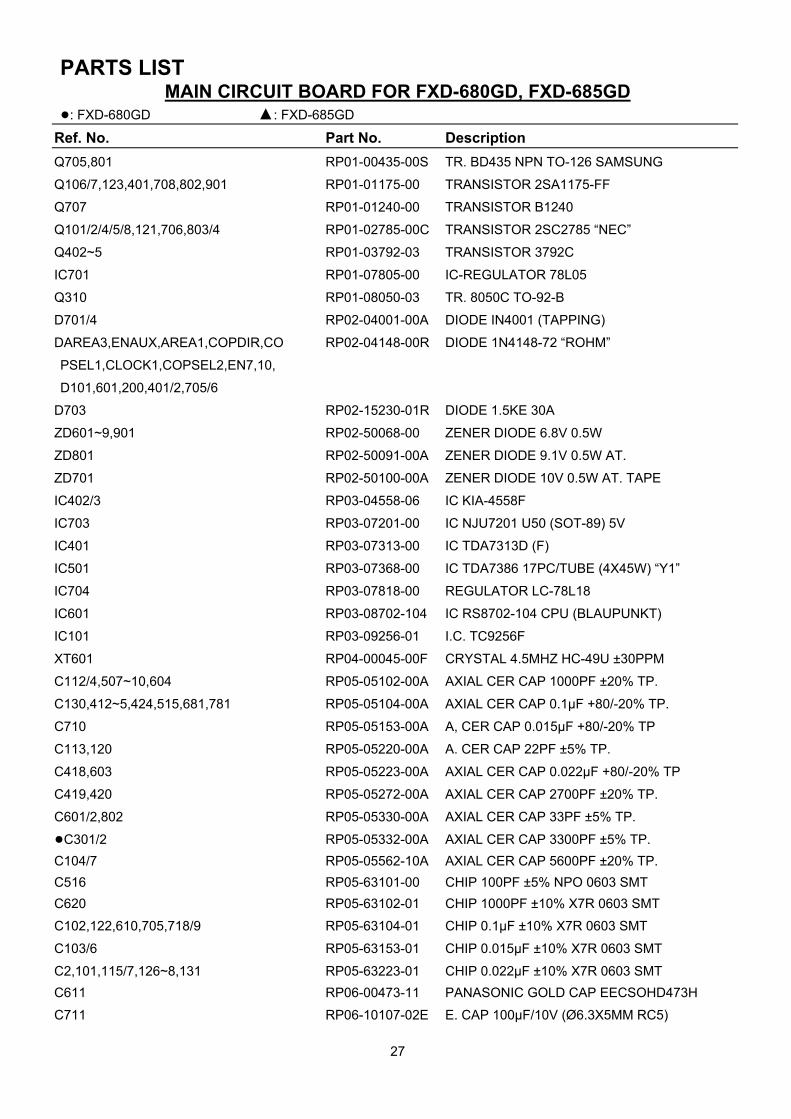
PARTS LIST MAIN CIRCUIT BOARD FOR FXD-680GD, FXD-685GD
: FXD-680GD : FXD-685GD Ref. No. Part No. Description Q705,801
Q106/7,123,401,708,802,901
Q707
Q101/2/4/5/8,121,706,803/4
Q402~5
IC701
Q310
D701/4
DAREA3,ENAUX,AREA1,COPDIR,CO
PSEL1,CLOCK1,COPSEL2,EN7,10,
D101,601,200,401/2,705/6
D703
ZD601~9,901
ZD801
ZD701
IC402/3
IC703
IC401
IC501
IC704
IC601
IC101
XT601
C112/4,507~10,604
C130,412~5,424,515,681,781
C710
C113,120
C418,603
C419,420
C601/2,802
C301/2 C104/7 C516 C620
C102,122,610,705,718/9
C103/6
C2,101,115/7,126~8,131 C611
C711
RP01-00435-00S
RP01-01175-00
RP01-01240-00
RP01-02785-00C
RP01-03792-03
RP01-07805-00
RP01-08050-03
RP02-04001-00A
RP02-04148-00R
RP02-15230-01R
RP02-50068-00
RP02-50091-00A
RP02-50100-00A
RP03-04558-06
RP03-07201-00
RP03-07313-00
RP03-07368-00
RP03-07818-00
RP03-08702-104
RP03-09256-01
RP04-00045-00F
RP05-05102-00A
RP05-05104-00A
RP05-05153-00A
RP05-05220-00A
RP05-05223-00A
RP05-05272-00A
RP05-05330-00A
RP05-05332-00A RP05-05562-10A RP05-63101-00 RP05-63102-01
RP05-63104-01
RP05-63153-01
RP05-63223-01 RP06-00473-11
RP06-10107-02E
TR. BD435 NPN TO-126 SAMSUNG
TRANSISTOR 2SA1175-FF
TRANSISTOR B1240
TRANSISTOR 2SC2785 “NEC”
TRANSISTOR 3792C
IC-REGULATOR 78L05
TR. 8050C TO-92-B
DIODE IN4001 (TAPPING)
DIODE 1N4148-72 “ROHM”
DIODE 1.5KE 30A
ZENER DIODE 6.8V 0.5W
ZENER DIODE 9.1V 0.5W AT.
ZENER DIODE 10V 0.5W AT. TAPE
IC KIA-4558F
IC NJU7201 U50 (SOT-89) 5V
IC TDA7313D (F)
IC TDA7386 17PC/TUBE (4X45W) “Y1”
REGULATOR LC-78L18
IC RS8702-104 CPU (BLAUPUNKT)
I.C. TC9256F
CRYSTAL 4.5MHZ HC-49U ±30PPM
AXIAL CER CAP 1000PF ±20% TP.
AXIAL CER CAP 0.1µF +80/-20% TP.
A, CER CAP 0.015µF +80/-20% TP
A. CER CAP 22PF ±5% TP.
AXIAL CER CAP 0.022µF +80/-20% TP
AXIAL CER CAP 2700PF ±20% TP.
AXIAL CER CAP 33PF ±5% TP.
AXIAL CER CAP 3300PF ±5% TP. AXIAL CER CAP 5600PF ±20% TP. CHIP 100PF ±5% NPO 0603 SMT CHIP 1000PF ±10% X7R 0603 SMT
CHIP 0.1µF ±10% X7R 0603 SMT
CHIP 0.015µF ±10% X7R 0603 SMT
CHIP 0.022µF ±10% X7R 0603 SMT PANASONIC GOLD CAP EECSOHD473H
E. CAP 100µF/10V (Ø6.3X5MM RC5)

28
MAIN CIRCUIT BOARD FOR FXD-680GD, FXD-685GD
: FXD-680GD : FXD-685GD Ref. No. Part No. Description C410 C123/5 C517/8 C605,612,707 C405,417,703/4/6/8,801 C416 C513 C119,129,152,502,619,709,782,901 C109 C437 C421/2 C105/8,118,401~4/6~9,411,427,503~6
,810/1, 430/2/4/5, 304/5,434/5 C501 R711 R123/6 R735 R116,125,618,709,721/2,733 R624, 402~5, 404/5 R119,120/1,714,804 R107,113,443,712/5 R152,426,810 R307,623/5,630 R814/5 R160 R122 R619 R631
R444,451,460/1,603/8,611~3/7,632,818
,903
R105/6,414/9,607,633,729,730/2,803
R127
R303/5
R128
R112,702
R109,816/7
R435~8 R718
R902
R802
RP06-10227-02N RP06-10476-01C RP06-16106-02 RP06-16106-02E RP06-16107-02E RP06-16226-02E RP06-16338-00S RP06-16476-02E RP06-50105-02 RP06-50105-02E RP06-50224-02E RP06-50225-02E RP06-50474-02E RP07-05010-10 RP07-05022-16A RP07-05100-10 RP07-05100-16A RP07-05101-16A RP07-05102-16A RP07-05103-16A RP07-05104-16A RP07-05105-16A RP07-05123-16A RP07-05124-54 RP07-05153-16A RP07-05220-16A RP07-05221-16A
RP07-05222-16A
RP07-05223-16A
RP07-05224-54
RP07-05272-16A
RP07-05330-16A
RP07-05331-16A
RP07-05332-16A
RP07-05333-16A
RP07-05334-16A
RP07-05393-16A
RP07-05471-16A
E. CAP 220µF 10V Ø8X5MM 105°C E. CAP 47µF 10V (Ø5X7MM MINI) E. CAP 10µF 16V (Ø6.3X5MM) E. CAP 10µF 16V (Ø4X5MM RC3) E. CAP 100µF 16V (Ø8X5) ELNA E. CAP 22µF 16V (Ø5X5) ELNA E. CAP 3300µF 16V 105°C E. CAP 47µF 16V (Ø6.3X5MM RC3) E. CAP 1µF 50V (Ø3X5MM) E. CAP 1µF 50V (Ø4X5MM RC3) E. CAP 0.22µF 50V (Ø3X5) ±20% ELNA E. CAP 2.2µF 50V (4X5MM RC03) E. CAP 0.47µF 50V (4X5MM RC03) RES. 1Ω 1/2W RES. 2.2Ω 1/16W (TAPPING) RES. 10Ω 1/2W RES. 10Ω 1/16W (TAPPING) RES. 100Ω 1/16W (TAPPING) RES. 1kΩ 1/16W (TAPPING) RES. 10kΩ 1/16W(TAPPING) RES. 100kΩ 1/16W (TAPPING) RES. 1MΩ 1/16W (TAPPING) RES. 12kΩ 1/16W (TAPPING) CHIP RES. 120kΩ 1/10W RES. 15kΩ 1/16W (TAPPING) RES. 22Ω 1/16W (TAPPING) RES. 220Ω 1/16W (TAPPING)
RES. 2.2kΩ 1/16W (TAPPING)
RES. 22kΩ 1/16W (TAPPING)
CHIP RES. 220kΩ 1/10W
RES. 2.7kΩ 1/16W (TAPPING)
RES. 33Ω 1/16W (TAPPING)
RES. 330Ω 1/16W (TAPPING)
RES. 3.3kΩ 1/16W (TAPPING)
RES. 33kΩ 1/16W (TAPPING)
RES. 330kΩ 1/16W (TAPPING)
RES. 39kΩ 1/16W (TAPPING)
RES. 470Ω 1/16W (TAPPING)

29
MAIN CIRCUIT BOARD FOR FXD-680GD, FXD-685GD : FXD-680GD : FXD-685GD
Ref. No. Part No. Description R115,151/3,427~30,502,602/4/5/6,622/6
~9,634,806,813
R154,406~9,411/2/6/7,425,501,601/9,
610/4~6,621,716,726,801/5/8,812
R439~42
R420/1,902
R401,424
R710
R101/3,410/3/5/8,431~4
R701
R302/4
R717,727
R445~8
R728,731
R156,508,720,736
R620
R449,452~4
R118
R102/4
R809
R110,713,807
R124
R725
L101
F1
MB
ISO
L701
SW1
CON6
RCA AUX IN
RCA
CON2
POWER WIRE
SPK WIRE
FM TUNER
RP07-05472-16A
RP07-05473-16A
RP07-05474-16A
RP07-05562-16A
RP07-05680-16A
RP07-05681-16A
RP07-05682-16A
RP07-05750-00
RP07-05822-16A
RP07-05823-16A
RP07-63102-00
RP07-63103-00
RP07-63104-00
RP07-63220-00
RP07-63223-00
RP07-63331-00
RP07-63332-00
RP07-63334-00
RP07-63473-00
RP07-63683-00
RP07-63823-00
RP09-70100-01
RP09-80006-00
RP11-17021-025
RP12-12068-411
RP15-00003-05
RP16-00244-00
RP25-08370-16
RP25-17020-02
RP25-17020-04
RP25-17068-36D
RP25-M1702-50
RP25-M1702-80
RP29-00347-02
RES. 4.7kΩ 1/16W (TAPPING)
RES. 47kΩ 1/16W (TAPPING)
RES. 470kΩ 1/16W (TAPPING)
RES. 5.6kΩ 1/16W (TAPPING)
RES. 68Ω 1/16W (TAPPING)
RES. 680Ω 1/16W (TAPPING)
RES. 6.8kΩ 1/16W (TAPPING)
RES. 75Ω 1/4W
RES. 8.2kΩ 1/16W (TAPPING)
RES. 82kΩ 1/16W (TAPPING)
CHIP RES. 1kΩ ±5% 0603 SMT
CHIP RES. 10kΩ ±5% 0603 SMT
CHIP RES. 100kΩ ±5% 0603 SMT
CHIP RES. 22Ω ±5% 0603 SMT
CHIP RES. 22kΩ ±5% 0603 SMT
CHIP RES. 330Ω ±5% 0603 SMT
CHIP RES. 3.3kΩ ±5% 0603 SMT
CHIP RES. 330kΩ
CHIP RES. 47kΩ ±5% 0603 SMT
CHIP RES. 68kΩ ±5% 0603 SMT
CHIP RES. 82kΩ ±5% 0603 SMT
MICRO INDUCTOR 10UH AXIAL TYPE
BAND PASS FILTER GFMB6-T
CD1702X3.6MB 186.5X146.5X1.6MM
PCB OPC-17068Y ISO BD D/S 42X42.2X1.2
TDROIO COIL L=105µH Ø1.0MM
TACT SWITCH TC-244 H=6.85MM
FPC-H1.25 CONNECTOR 16PIN
CD1702 AUX&RCA P=2.0 L=250
CD1702 RCA2 P=2.0 L=250
36PIN ISO SOCKET (NO RCA)
ISO SKT 5PIN POWER SANYO
ISO SKT 8PIN SPK SANYO
MITSVMI TUNER FAE-347-A29

30
KEY CIRCUIT BOARD FOR FXD-680GD, FXD-685GD
Ref. No. Part No. Description ZD101
LED1
LED2~25
BL
IC101
C102
C101
R138,153~5
R126/7
R107,118
R108,119
R101/2
R131
R113,124
R103,114
R109,120,132/4/6,159
R104,115
R110,121,155
R105,116
R111,122/5
R128
R130
R106,117,137
R135
R112,123
KB
VOL
SOCK
LCD
RP02-00062-07
RP02-01112-02
RP 02-01112-03F
RP02-A1702-23
RP03-75823-00
RP05-63104-01
RP05-63681-00
RP07-63000-00
RP07-63100-00
RP07-63102-00
RP07-63152-00
RP07-63181-00
RP07-63182-00
RP07-63183-00
RP07-63221-00
RP07-63222-00
RP07-63331-00
RP07-63332-00
RP07-63471-00
RP07-63472-00
RP07-63513-00
RP07-63561-00
RP07-63681-00
RP07-63821-00
RP07-63822-00
RP11-17020-305
RP16-01107-02K
RP18-00163-00
RP25-M1475-00
RP27-17020-00
E.S.D. DIODE NNCD6.2G (5PIN)
SMD LED FR1112H (RED) STANLEY
FA1112H (ORANGE) SMD LED “STANLEY”
CD1702 LCD B.L. 97X17 AMBER
IC LC75823ED
CHIP 0.1µF ±10% X7R 0603 SMT
CHIP 680PF ±5% NPO 0603 SMT
CHIP RES. 0Ω 0603 SMT
CHIP RES. 10Ω ±5% 0603 SMT
CHIP RES. 1kΩ ±5% 0603 SMT
CHIP RES. 1.5kΩ ±5% 0603 SMT
CHIP RES. 180Ω ±5% 0603 SMT
CHIP RES. 1.8kΩ ±5% 0603 SMT
CHIP RES. 18kΩ ±5% 0603 SMT
CHIP RES. 220Ω ±5% 0603 SMT
CHIP RES. 2.2kΩ ±5% 0603 SMT
CHIP RES. 330Ω ±5% 0603 SMT
CHIP RES. 3.3kΩ ±5% 0603 SMT
CHIP RES. 470Ω ±5% 0603 SMT
CHIP RES. 4.7kΩ ±5% 0603 SMT
CHIP RES. 51kΩ ±5% 0603 SMT
CHIP RES. 560Ω ±5% 0603 SMT
CHIP RES. 680Ω ±5% 0603 SMT
CHIP RES. 820Ω ±5% 0603 SMT
CHIP RES. 8.2kΩ ±5% 0603 SMT
CD1702X3.6/3.7 KB D/S 42X168X1.6MM
TACT SW. KIE KPT-1107CD 4.3M 2PIN RED
ENCODER SRGP200200 (ALPS)
15PIN SKT R41/1475A (KENWOOD)
CDD-1702X3.6/X3.7 LCD TN/POS
31
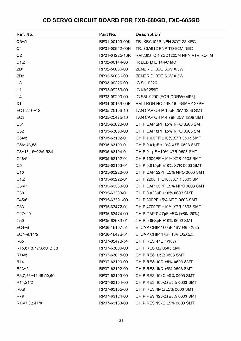
CD SERVO CIRCUIT BOARD FOR FXD-680GD, FXD-685GD
Ref. No. Part No. Description Q3~5
Q1
Q2
D1,2
ZD1
ZD2
U3
U1
U4
X1
EC1,2,10~12
EC3
C31
C32
C34/5
C36~43,58
C3~13,15~23/6,52/4
C48/9
C51
C10
C1,2
C56/7
C30
C45/6
C33
C27~29
C50
EC4~6
EC7~9,14/5
R85
R15,67/8,72/3,80~2,88
R74/5
R14
R23~5
R3,7,38~41,49,50,66
R11,21/2
R8,9
R78
R16/7,32,47/8
RP01-00103-00K
RP01-00812-00N
RP01-01225-13R
RP02-00144-00
RP02-50036-00
RP02-50056-00
RP03-09226-00
RP03-09259-00
RP03-09290-00
RP04-00169-00R
RP05-25106-10
RP05-25475-10
RP05-63020-00
RP05-63080-00
RP05-63102-01
RP05-63103-01
RP05-63104-01
RP05-63152-01
RP05-63153-01
RP05-63220-00
RP05-63222-01
RP05-63330-00
RP05-63333-01
RP05-63391-00
RP05-63472-01
RP05-63474-00
RP05-63683-01
RP06-16107-54
RP06-16476-54
RP07-05470-54
RP07-63000-00
RP07-63015-00
RP07-63100-00
RP07-63102-00
RP07-63103-00
RP07-63104-00
RP07-63105-00
RP07-63124-00
RP07-63153-00
TR. KRC103S NPN SOT-23 KEC
TR. 2SA812 PNP TO-92M NEC
RANSISTOR 2SD1225M NPN ATV ROHM
IR LED MIE 144A1MC
ZENER DIODE 3.6V 0.5W
ZENER DIODE 5.6V 0.5W
IC SIL 9226
IC KA9259D
IC S5L 9290 (FOR CDRW+MP3)
RALTRON HC-49S 16.934MHZ 27PF
TAN CAP CHIP 10µF 25V 1206 SMT
TAN CAP CHIP 4.7µF 25V 1206 SMT
CHIP CAP 2PF ±5% NPO 0603 SMT
CHIP CAP 8PF ±5% NPO 0603 SMT
CHIP 1000PF ±10% X7R 0603 SMT
CHIP 0.01µF ±10% X7R 0603 SMT
CHIP 0.1µF ±10% X7R 0603 SMT
CHIP 1500PF ±10% X7R 0603 SMT
CHIP 0.015µF ±10% X7R 0603 SMT
CHIP CAP 22PF ±5% NPO 0603 SMT
CHIP 2200PF ±10% X7R 0603 SMT
CHIP CAP 33PF ±5% NPO 0603 SMT
CHIP 0.033µF ±10% 0603 SMT
CHIP 390PF ±5% NPO 0603 SMT
CHIP 4700PF ±10% X7R 0603 SMT
CHIP CAP 0.47µF ±5% (+80/-20%)
CHIP 0.068µF ±10% 0603 SMT
E. CAP CHIP 100µF 16V Ø6.3X5.5
E. CAP CHIP 47µF 16V Ø5X5.5
CHIP RES 47Ω 1/10W
CHIP RES 0Ω 0603 SMT
CHIP RES 1.5Ω 0603 SMT
CHIP RES 10Ω ±5% 0603 SMT
CHIP RES 1kΩ ±5% 0603 SMT
CHIP RES 10kΩ ±5% 0603 SMT
CHIP RES 100kΩ ±5% 0603 SMT
CHIP RES 1MΩ ±5% 0603 SMT
CHIP RES 120kΩ ±5% 0603 SMT
CHIP RES 15kΩ ±5% 0603 SMT
32
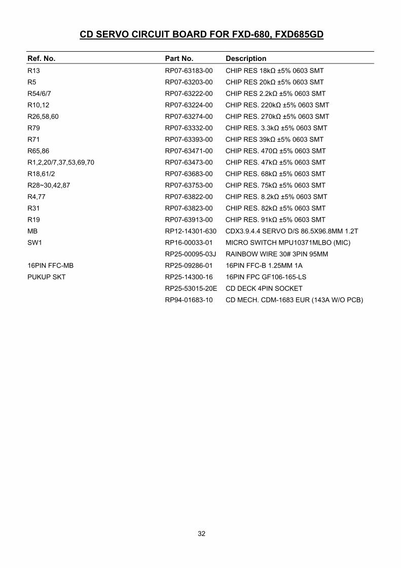
CD SERVO CIRCUIT BOARD FOR FXD-680, FXD685GD
Ref. No. Part No. Description R13
R5
R54/6/7
R10,12
R26,58,60
R79
R71
R65,86
R1,2,20/7,37,53,69,70
R18,61/2
R28~30,42,87
R4,77
R31
R19
MB
SW1
16PIN FFC-MB
PUKUP SKT
RP07-63183-00
RP07-63203-00
RP07-63222-00
RP07-63224-00
RP07-63274-00
RP07-63332-00
RP07-63393-00
RP07-63471-00
RP07-63473-00
RP07-63683-00
RP07-63753-00
RP07-63822-00
RP07-63823-00
RP07-63913-00
RP12-14301-630
RP16-00033-01
RP25-00095-03J
RP25-09286-01
RP25-14300-16
RP25-53015-20E
RP94-01683-10
CHIP RES 18kΩ ±5% 0603 SMT
CHIP RES 20kΩ ±5% 0603 SMT
CHIP RES 2.2kΩ ±5% 0603 SMT
CHIP RES. 220kΩ ±5% 0603 SMT
CHIP RES. 270kΩ ±5% 0603 SMT
CHIP RES. 3.3kΩ ±5% 0603 SMT
CHIP RES 39kΩ ±5% 0603 SMT
CHIP RES. 470Ω ±5% 0603 SMT
CHIP RES. 47kΩ ±5% 0603 SMT
CHIP RES. 68kΩ ±5% 0603 SMT
CHIP RES. 75kΩ ±5% 0603 SMT
CHIP RES. 8.2kΩ ±5% 0603 SMT
CHIP RES. 82kΩ ±5% 0603 SMT
CHIP RES. 91kΩ ±5% 0603 SMT
CDX3.9.4.4 SERVO D/S 86.5X96.8MM 1.2T
MICRO SWITCH MPU10371MLBO (MIC)
RAINBOW WIRE 30# 3PIN 95MM
16PIN FFC-B 1.25MM 1A
16PIN FPC GF106-165-LS CD DECK 4PIN SOCKET
CD MECH. CDM-1683 EUR (143A W/O PCB)

33
REMOTE CIRCUIT BOARD FOR FXD-680GD, FXD-685GD
Ref. No. Part No. Description Q500
LD1
D500/1
IC500
C504
C501/2
R501
R502
CF501
PCB
RP01-01781-18
RP02-00334-00
RP02-04148-00
RP03-00101-00
RP05-03105-10M
RP05-03121-06
RP07-05022-54
RP07-05102-54
RP09-50455-05J
RP11-17020-505
TR. 2SD1781K-R “ROHM”
INFRARED LED Ø3MM MIE-334A4
DIODE IN-4148
IC S0101 (SGNEC)
CHIP CAP KC20E1C105M-TS
CHIP CAP. 120PF (NPO)
CHIP RES. 2.2Ω 1/10W
CHIP RES 1kΩ 1/10W
CER RESONATOR ZTB455E
CD1702 RC06 D/S 1.2X80.3X51.5 SANYO
34
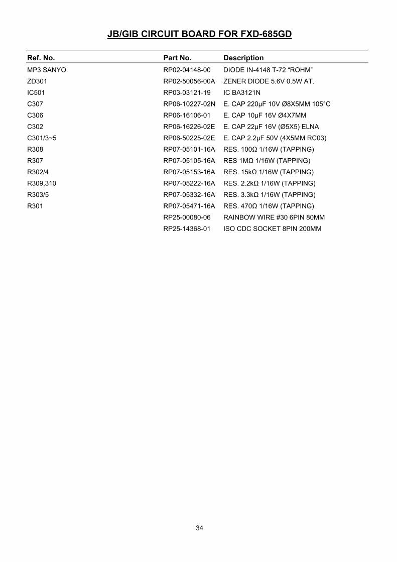
JB/GIB CIRCUIT BOARD FOR FXD-685GD
Ref. No. Part No. Description MP3 SANYO
ZD301
IC501
C307
C306
C302
C301/3~5
R308
R307
R302/4
R309,310
R303/5
R301
RP02-04148-00
RP02-50056-00A
RP03-03121-19
RP06-10227-02N
RP06-16106-01
RP06-16226-02E
RP06-50225-02E
RP07-05101-16A
RP07-05105-16A
RP07-05153-16A
RP07-05222-16A
RP07-05332-16A
RP07-05471-16A
RP25-00080-06
RP25-14368-01
DIODE IN-4148 T-72 “ROHM”
ZENER DIODE 5.6V 0.5W AT.
IC BA3121N
E. CAP 220µF 10V Ø8X5MM 105°C
E. CAP 10µF 16V Ø4X7MM
E. CAP 22µF 16V (Ø5X5) ELNA
E. CAP 2.2µF 50V (4X5MM RC03)
RES. 100Ω 1/16W (TAPPING)
RES 1MΩ 1/16W (TAPPING)
RES. 15kΩ 1/16W (TAPPING)
RES. 2.2kΩ 1/16W (TAPPING)
RES. 3.3kΩ 1/16W (TAPPING)
RES. 470Ω 1/16W (TAPPING)
RAINBOW WIRE #30 6PIN 80MM
ISO CDC SOCKET 8PIN 200MM

35
SCHEMATIC DIAGRAM – MAIN BOARD FOR FXD-680GD & FXD-685GD

36
SCHEMATIC DIAGRAM – KEY BOARD FOR FXD-680GD & FXD-685GD
37
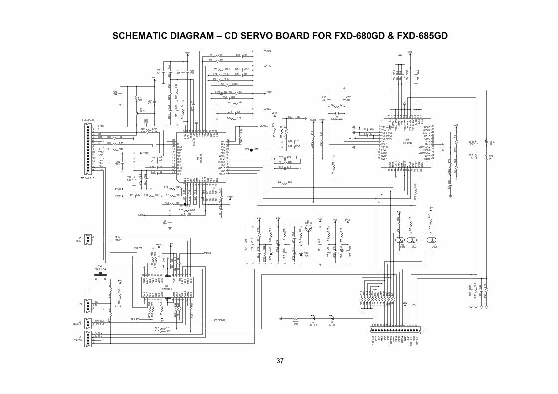
SCHEMATIC DIAGRAM – CD SERVO BOARD FOR FXD-680GD & FXD-685GD
38
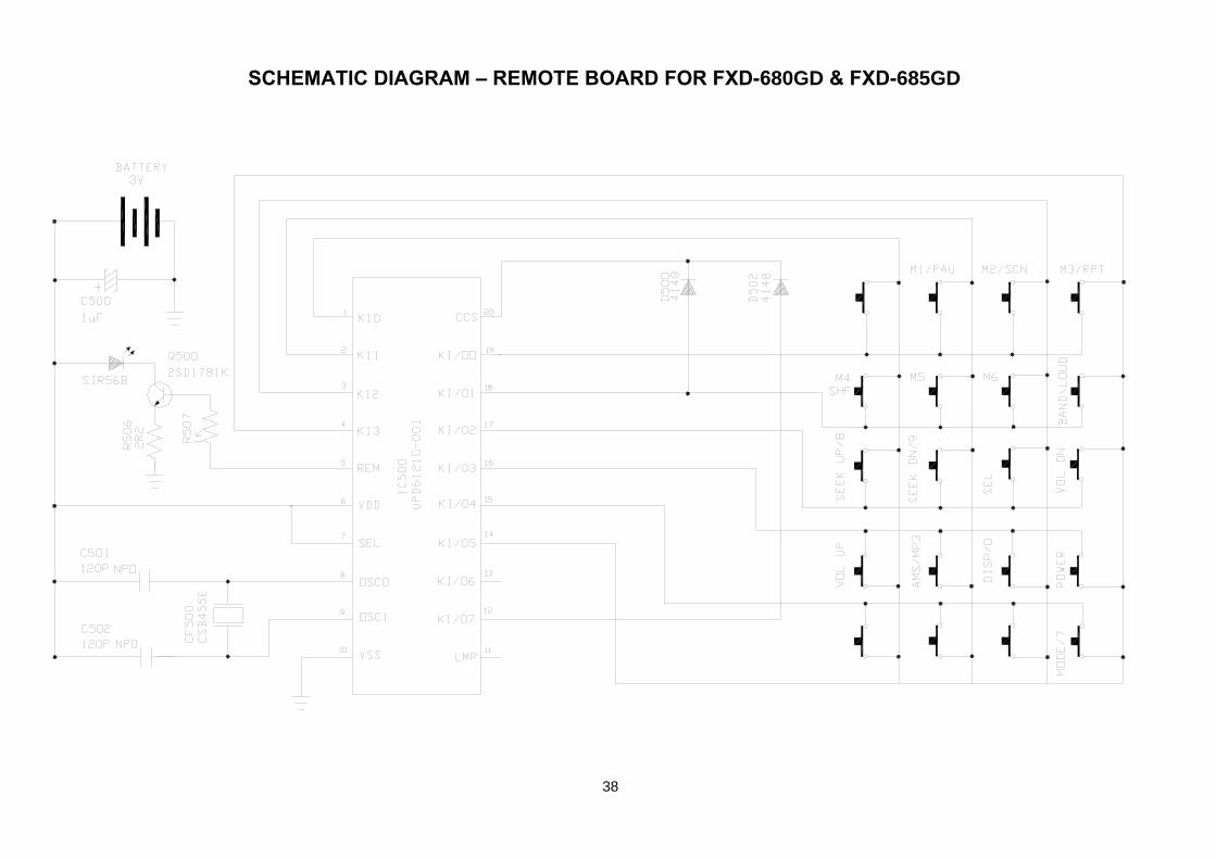
SCHEMATIC DIAGRAM – REMOTE BOARD FOR FXD-680GD & FXD-685GD

39
SCHEMATIC BOARD DIAGRAM – MAIN FOR FXD-680GD & FXD-685GD

40
SCHEMATIC BOARD DIAGRAM – KEY FOR FXD-680GD & FXD685G
SCHEMATIC BOARD DIAGRAM – ISO FOR FXD-680GD FXD-685GD
41
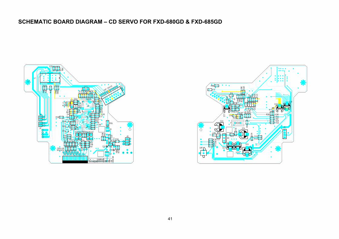
SCHEMATIC BOARD DIAGRAM – CD SERVO FOR FXD-680GD & FXD-685GD

42
SCHEMATIC BOARD DIAGRAM – REMOTE FOR FXD-680GD & FXD-685GD

FXD-680GD FXD-685GD
No. 1702YI3944 Printed In China issue date 27-04