SERVICE MANUAL COLOR MONITOR NEC MultiSync 20WGX2 MODEL ID : 20WGX2-BK(B)
143
SERVICE MANUAL COLOR MONITOR MultiSync 20WGX 2 MODEL ID : 20WGX 2 -BK(B) 1st Edition NEC DISPLAY SOLUTIONS, LTD. DECEMBER 2005 VERY IMPORTANT! This Equipment is compatible with RoHS Directive and Lead-Free. Since the equipment is compatible with RoHS Directive, use components in which the use of specific chemically noxious substances is restricted; use only designated spare parts when it is necessary to replace such parts with new parts. Use lead-free solder for the equipment compatible with ones with substrates on which lead-free components are mounted. For the details, refer to “Caution for Lead-Free Solder- ing Work” given in the next page. ® PART NO : 599910796 200603 08GJ5LBG
Transcript of SERVICE MANUAL COLOR MONITOR NEC MultiSync 20WGX2 MODEL ID : 20WGX2-BK(B)
SERVICE MANUAL
COLOR MONITOR
MultiSync 20WGX2
MODEL ID : 20WGX2-BK(B)
1st Edition
NEC DISPLAY SOLUTIONS, LTD.
DECEMBER 2005
VERY IMPORTANT!
This Equipment is compatible with RoHS Directive and Lead-Free.
Since the equipment is compatible with RoHS Directive, use components in which the use
of specific chemically noxious substances is restricted; use only designated spare parts
when it is necessary to replace such parts with new parts.
Use lead-free solder for the equipment compatible with ones with substrates on which
lead-free components are mounted. For the details, refer to “Caution for Lead-Free Solder-
ing Work” given in the next page.
®
PART NO : 599910796
200603
08GJ5LBG

1. Safety guideline in servicing 1) Never touch the portions with the marking ( ). Serious injury or even death may result.
2) Do not expose the set to rain or water. A risk of fire or electric shock can result.
3) Use an adequate power cord. A risk of fire or electric shock can result.
4) Do not attempt to service or modify the set without prior permission of the manufacturer. A risk of fire or electric shock can result.
5) Leave the maintenance service to a service engineer having qualification, knowledge and experience.
A risk of electric shock, injury or fire can result.
6) Always employ genuine parts indicated in the service manual for replacement. A risk of fire or electric shock can result.
7) In reassembling use the specified binding bands, clampers, tubes and barriers--all of which are necessary for insulation/protection--in their original positions.
A risk of fire or electric shock can result.
2. Other cautions necessary 1) When removing the cables from their connectors, take care not to damage the wire portions so as to
prevent the occurrence of poor contact.
2) When attaching/detaching screws, use a screwdriver that is well-fit to the screw size.
3. Caution for LEAD-FREE soldering work For this equipment, parts compatible with lead-free materials are used. Please observe the following precautions, when performing any soldering work.
1) Use lead-free solder for substrates mounted with lead-free parts. If you use eutectic solder by mistake, solder will not fuse well because of the difference in fusion point.
2) Fusion Point Lead-free solder: 220°C
Eutectic solder : 183°C
3) Solder composition of Lead-free solder: Sn-3.0Ag-0.5Cu [Maker] [Type] Nihon Genma DHB-RMA NP303-### Senju metal ESC F3 M705E-### (#:This mark shows the diameter of the solder wire.)
4) Use without fail a temperature adjustable soldering iron for working with lead-free solder. Moreover, the power consumption of the soldering iron must use from 25W to 75W.
[Solder Iron tip temperature and contact time] Category of Parts Lead-free solder Eutectic solder
*SMD Chip The Parts of Chip type 300-320°C (1-3sec)
260-280°C (1-3sec)
*SMD QFP The Parts (IC) of Quad Flat Pack Package type 320-350°C (1-3sec)
280-300°C (1-3sec)
Heat sink Heat sink 360-380°C (1-3sec)
320-420°C (1-3sec)
Ax,RD The Parts of Axial or Radial type (The Electric Parts other than the above-mentioned. Ex.: IC, Transistor, Resistor, Capacitor)
340-370°C (1-3sec)
350-390°C (1-3sec)
*SMD: Surface Mounting Device

Specification Item
Analog Input Digital Input LPL LM201WE2-SLA1
Size 20.1" (51.1133cm) Active Display Area 433.44 (H) x 270.90 (V) mm Resolution 1680x1050 dots (WSXGA+) Pixel Pitch 0.258mm Color Depth 16,77 M color (8-bits) Luminance 470cd/m2(Typ.) *1)
CR>10 Up 89 / Down 89 / Left 89 / Right 89 (Typ.) Viewing Angle(Typ.) CR>5 -
Contrast Ratio 700:1(Typ.) 1600:1 (Typ.) (Advanced DV mode ON!)
ON+OFF 12ms Response Time GTG 6ms by overdrive circuit integrated in panel
Color gamut > 72% Surface Treatment Glare (AR<2.0%)
LCD
Back Light CCFL x 10pcs (Direct Light Type) Horizontal frequency 24.7kHz - 81.2kHz 24.7kHz - 81.2kHz Vertical frequency 49.0Hz - 76.0 Hz Video Signal Analog RGB Digital RGB
Sync. Signal Separate Sync.(TTL) Composite Sync.on Green video
TMDS
Pixel Clock 25.2MHz - 165MHz
Input Signals
Input connector Mini D-sub 15Pin DVI-D Preset Timings User preset : 23
USB Hub (only AN/BNBK) USB Version 2.0 Self Powered Hub 1 upstream / 4 down stream
Front Control Menu/Exit, Direction (4 direction key), Select/1<->2, Reset/DV mode, Power (DC)
Back side Power (AC)
OSM
Brightness, Contrast, Auto contrast, Advanced DV mode, DV mode, Auto adjust, H Position, V position, H size, Fine, Color control, Sharpness, Expansion mode, Off timer, LED Brightness, Hot key, Factory preset, Language, OSM Left/Right, OSM Down/Up, OSM turn off, OSM Lock out, Resolution notifier, Monitor inf.
Functions
Remote Control VESA DDC/CI Safety UL/ cUL , TuV GS, CE, CB Report, PSB EMC FCC Class B, Canadian DOC Class B, C-tick Class B, CE VLF / ELF MPR-II, MPRIII, TCO' 03 Power Management VESA DPMS ,EPA, Energy star Ver 4.0 Tier2, GEEA label Ergonomics TUV/ERGONOMIE Plug and Play VESA DDC2B
Regulations
Others US Mercury Regulation, Windows XP/2000 Logo Temperature 5-35 degree C Environment
Condition Humidity 10-80% (without condensation) Input Voltage AC100-240V, 50 / 60Hz
Typ 84 W max (1.0 A @ 100 - 120V, 0.52 A @ 220 - 240V) Power consumption Power
saving <2.3W with USB hub model, <2W without USB hub (DPMS) <1W (DC Power Off) Meet to Energy Star Ver 4.0 Tier 2
Power Supply
Input Connector 3P IEC Type Weight with Stand Approx. 6.3 kg
without Stand Approx. 4.6 kg Net 471.4 (W) x 391.5(H) x 203.0(D) mm Dimension
Gross 570.0(W) x 518.0(H) x 262.0(D) mm VESA compatible arm mounting interface 100mmx100mm Tilt / Swivel / Rotation / Height Adjustment Up & Down 30deg to -5deg / Yes +/- 170degree / NA / NA
AC Power code 2.0m
Signal Cable 2.0m : minD-sub15pin - minD-sub15pin 2.0m: DVI-D - DVI-D
Accessories
Others User's manual, USB cable, etc. *1)60% of a mass-product should meet
Product Specifications

CONTENTS
Page No.
USER’S MANUAL ................................................................................................... 1-1
SERIAL NUMBER INFORMATION .......................................................................... 2-1
DISASSEMBLY........................................................................................................ 3-1
ADJUSTMENT PROCEDURES .............................................................................. 4-1
INSPECTION ........................................................................................................... 5-1
TROUBLE SHOOTING ............................................................................................ 6-1
CIRCUIT DESCRIPTION ......................................................................................... 7-1
REPLACEMENT PARTS LIST ................................................................................ 8-1
BLOCK DIAGRAM ................................................................................................... 9-1
SCHEMATIC DIAGRAMS ...................................................................................... 10-1
PACKING SPECIFICATION ................................................................................... 11-1
REVISION HISTORY.............................................................................................. 12-1

MultiSync 20WGX 2User’s Manual
Index
Warning, Caution ........................................................................................................................ English-1
Declaration .................................................................................................................................. English-1
Canadian Department of Communications Compliance Statement ........................................... English-2
Declaration of Conformity ........................................................................................................... English-2
Contents ...................................................................................................................................... English-3
Quick Start .................................................................................................................................. English-4
Controls ....................................................................................................................................... English-8
Recommended use ..................................................................................................................... English-11
Specifications .............................................................................................................................. English-13
Features ...................................................................................................................................... English-14
Troubleshooting ........................................................................................................................... English-15
TCO’03 ........................................................................................................................................ English-16
Manufacturer’s Recycling and Energy Information...................................................................... English-17

Eng
lish
English-1
WARNING
CAUTIONCAUTION: TO REDUCE THE RISK OF ELECTRIC SHOCK, MAKE SURE POWER CORD IS UNPLUGGED FROM
WALL SOCKET. TO FULLY DISENGAGE THE POWER TO THE UNIT, PLEASE DISCONNECT THEPOWER CORD FROM THE AC OUTLET.DO NOT REMOVE COVER (OR BACK). NO USERSERVICEABLE PARTS INSIDE. REFER SERVICING TO QUALIFIED SERVICE PERSONNEL.
This symbol warns user that uninsulated voltage within the unit may have sufficient magnitude to causeelectric shock. Therefore, it is dangerous to make any kind of contact with any part inside this unit.
This symbol alerts the user that important literature concerning the operation and maintenance of this unithas been included. Therefore, it should be read carefully in order to avoid any problems.
Caution:When operating the MultiSync 20WGX2 with a 220-240V AC power source in Europe, use the power cord provided with themonitor.
In the UK, a BS approved power cord with a moulded plug has a Black (five Amps) fuse installed for use with this equipment.If a power cord is not supplied with this equipment please contact your supplier.
When operating the MultiSync 20WGX2 with a 220-240V AC power source in Australia, use the power cord provided with themonitor. If a power cord is not supplied with this equipment please contact your supplier.
For all other cases, use a power cord that matches the AC voltage of the power outlet and has been approved by andcomplies with the safety standard of your particular country.
TO PREVENT FIRE OR SHOCK HAZARDS, DO NOT EXPOSE THIS UNIT TO RAIN OR MOISTURE. ALSO, DO NOTUSE THIS UNIT'S POLARIZED PLUG WITH AN EXTENSION CORD RECEPTACLE OR OTHER OUTLETS UNLESSTHE PRONGS CAN BE FULLY INSERTED.
REFRAIN FROM OPENING THE CABINET AS THERE ARE HIGH VOLTAGE COMPONENTS INSIDE. REFERSERVICING TO QUALIFIED SERVICE PERSONNEL.
Declaration
Declaration of the Manufacturer
We hereby certify that the colour monitorMultiSync 20WGX2 (L205GJ) is incompliance with
Council Directive 73/23/EEC:– EN 60950-1
Council Directive 89/336/EEC:– EN 55022– EN 61000-3-2– EN 61000-3-3– EN 55024
and marked with
NEC Display Solutions, Ltd.4-13-23, Shibaura,
Minato-KuTokyo 108-0023, Japan
Windows is a registered trademark of Microsoft Corporation. NEC is a registered trademark of NEC Corporation. ENERGY STAR is aU.S. registered trademark.OmniColor is a registered trademark of NEC Display Solutions Europe GmbH in the countries of EU and Switzerland.ErgoDesign is a registered trademark of NEC Display Solutions, Ltd. in Austria, Benelux, Denmark, France, Germany, Italy, Norway,Spain, Sweden, U.K.NaViSet is a trademark of NEC Display Solutions Europe GmbH in the countries of EU and Switzerland.MultiSync is a registered trademark of NEC Display Solutions, Ltd. in the countries of U.K., Italy, Austria, Netherlands, Switzerland,Sweden, Spain, Denmark, Germany, Norway and Finland.All other brands and product names are trademarks or registered trademarks of their respective owners.As an ENERGY STAR® Partner, NEC Display Solutions of America, Inc. has determined that this product meets the ENERGY STAR guidelinesfor energy efficiency. The ENERGY STAR emblem does not represent EPA endorsement of any product or service.

English-2
Canadian Department of Communications ComplianceStatementDOC: This Class B digital apparatus meets all requirements of the Canadian Interference-Causing Equipment Regulations.
C-UL: Bears the C-UL Mark and is in compliance with Canadian Safety Regulations according to CAN/CSA C22.2 No. 60950-1.
FCC Information1. Use the attached specified cables with the MultiSync 20WGX2 (L205GJ) colour monitor so as not to interfere with radio
and television reception.
(1) The power supply cord you use must have been approved by and comply with the safety standards of U.S.A.,and meet the following condition.
Power supply cord Non shield type, 3-conductorLength 2.0 mPlug shape
U.S.A
(2) Please use the supplied shielded video signal cable and USB cable with ferrite cores. Use of other cables andadapters may cause interference with radio and television reception.
2. This equipment has been tested and found to comply with the limits for a Class B digital device, pursuant to part 15 ofthe FCC Rules. These limits are designed to provide reasonable protection against harmful interference in a residentialinstallation. This equipment generates, uses, and can radiate radio frequency energy, and, if not installed and used inaccordance with the instructions, may cause harmful interference to radio communications. However, there is noguarantee that interference will not occur in a particular installation. If this equipment does cause harmful interferenceto radio or television reception, which can be determined by turning the equipment off and on, the user is encouragedto try to correct the interference by one or more of the following measures:
• Reorient or relocate the receiving antenna.
• Increase the separation between the equipment and receiver.
• Connect the equipment into an outlet on a circuit different from that to which the receiver is connected.
• Consult your dealer or an experienced radio/TV technician for help.
If necessary, the user should contact the dealer or an experienced radio/television technician for additionalsuggestions. The user may find the following booklet, prepared by the Federal Communications Commission, helpful:“How to Identify and Resolve Radio-TV Interference Problems.” This booklet is available from the U.S. GovernmentPrinting Office, Washington, D.C., 20402, Stock No. 004-000-00345-4.
Declaration of ConformityThis device complies with Part 15 of FCC Rules. Operation is subject to the following two conditions. (1) This device may notcause harmful interference, and (2) this device must accept any interference received, including interference that may causeundesired operation.
U.S. Responsible Party: NEC Display Solutions of America, Inc.Address: 500 Park Blvd, Suite 1100
Itasca, Illinois 60143Tel. No.: (630) 467-3000
Type of Product: Display Monitor
Equipment Classification: Class B Peripheral
Model: MultiSync 20WGX2 (L205GJ)
We hereby declare that the equipment specified above conformsto the technical standards as specified in the FCC Rules.
Eng
lish
English-3
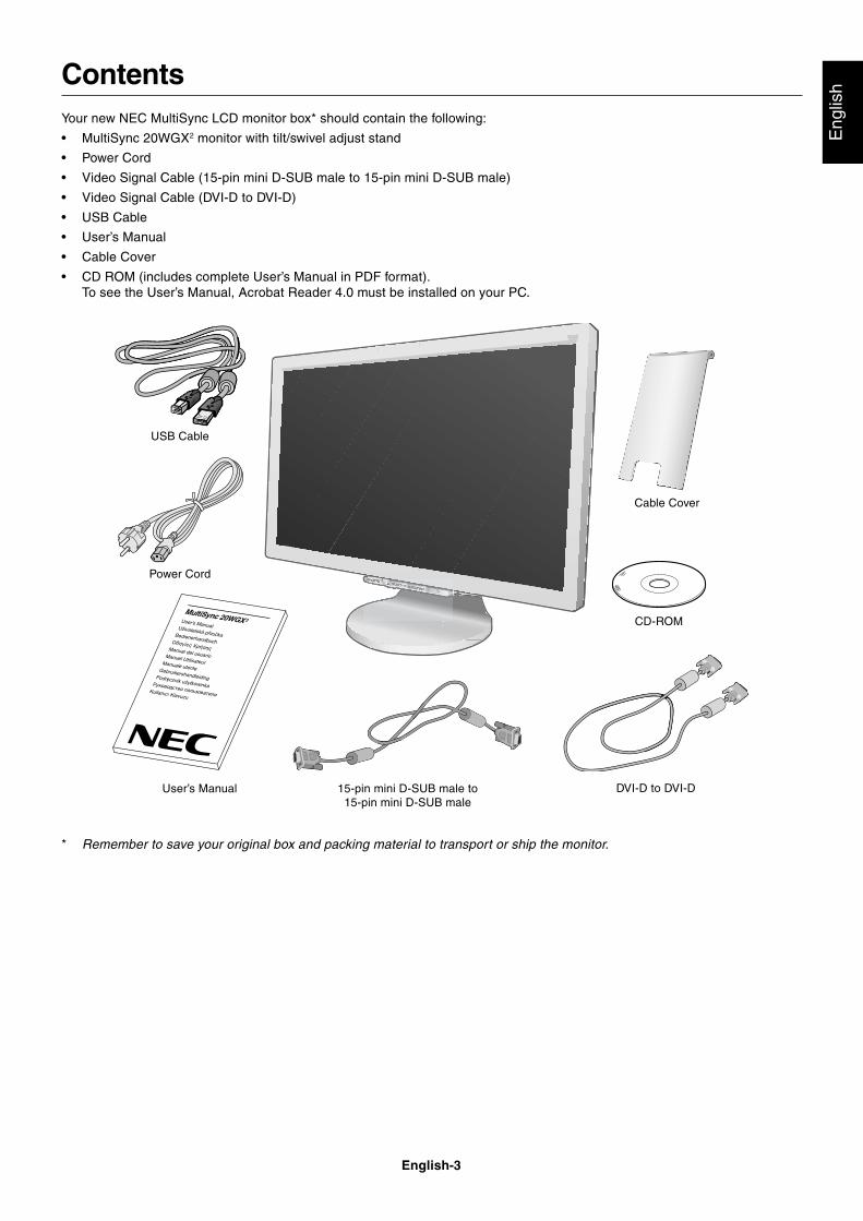
ContentsYour new NEC MultiSync LCD monitor box* should contain the following:
• MultiSync 20WGX2 monitor with tilt/swivel adjust stand
• Power Cord
• Video Signal Cable (15-pin mini D-SUB male to 15-pin mini D-SUB male)
• Video Signal Cable (DVI-D to DVI-D)
• USB Cable
• User’s Manual
• Cable Cover
• CD ROM (includes complete User’s Manual in PDF format).To see the User’s Manual, Acrobat Reader 4.0 must be installed on your PC.
* Remember to save your original box and packing material to transport or ship the monitor.
Power Cord
User’s Manual 15-pin mini D-SUB male to15-pin mini D-SUB male
CD-ROM
Cable Cover
USB Cable
DVI-D to DVI-D

English-4
Quick StartTo attach the MultiSync LCD monitor to your system, follow these instructions:
1. Turn off the power to your computer.
2. For the PC or MAC with DVI digital output: Connect the DVI signal cable to the connector of the display card in yoursystem (Figure A.1). Tighten all screws.
For the PC with Analog output: Connect the 15-pin mini D-SUB signal cable to the connector of the display card in yoursystem (Figure A.2). Tighten all screws.
For the MAC: Connect the Macintosh cable adapter to the computer, then attach the 15-pin mini D-SUB signal cable tothe Macintosh cable adapter (Figure B.1). Tighten all screws.
NOTE: Some Macintosh systems do not require a Macintosh cable adapter.
3. Remove the connector cover (Figure C.1).
4. Place hands on each side of the monitor to tilt the LCD panel 30 degrees angles (Figure C.2).
5. Connect all cables to the appropriate connectors through the square hole in the stand (Figure C.3).
Figure A.1 Figure B.1MacintoshCable Adapter(not included)
Figure A.2DVI signal cable
Figure C.1 Figure C.2
Figure C.3

Eng
lish
English-5
6. Place the connector cover onto the back cabinet (Figure C.4).
7. Place all cables into the hooks (Figure C.5).
8. Place hands on each side if the monitor to tilt the LCD panel back 5° (Figure C.6).
9. Place the cable cover onto the stand (Figure C.6). To remove the cable cover, push the notch at the bottom of the cover up(towards the top of the monitor) in order to unhook the cover from the stand (Figure C.7).
10. Connect the power cord to the power outlet (Figure D.1).
NOTE: Please refer to Caution section of this manual for proper selection of AC power cord.
11. The vacation switch on the back side of the monitor must be turned on (Figure D.1). Turn on the monitor with the frontpower button and the computer.
NOTE: The vacation switch is a true on/off switch. If this switch is on the OFF position, the monitor cannot be turned onusing the front button. DO NOT switch on/off repeatedly.
12. No-Touch Auto Adjust automatically adjusts the monitor to optimal settings upon initial setup for most timings.For further adjustments, use the following OSM controls:
• Auto Adjust Contrast (Analog input only)
• Auto Adjust (Analog input only)
Refer to the Controls section of this User’s Manual for a full description of these OSM controls.
NOTE: If you have any problems, please refer to the Troubleshooting section of this User’s Manual.
Figure C.6 Figure C.7
Figure C.4 Figure C.5
Figure D.1
OFF Position
ON Position Vacation Switch
English-6
Figure M.1
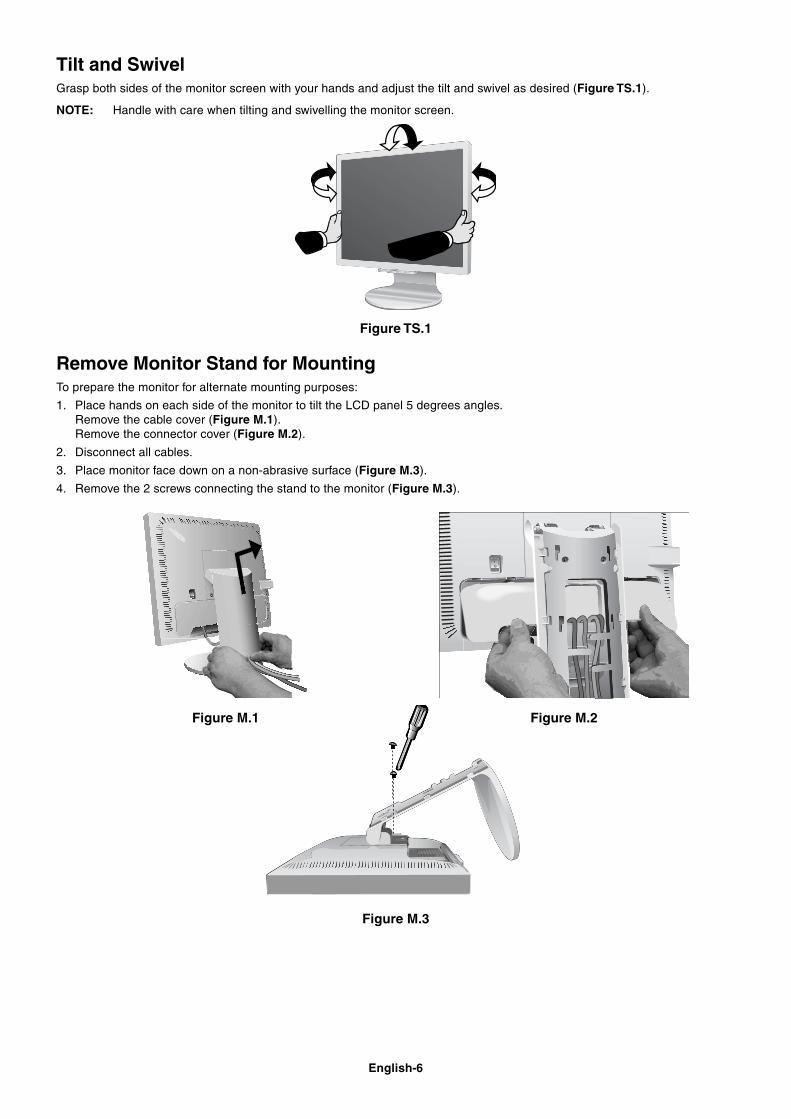
Remove Monitor Stand for MountingTo prepare the monitor for alternate mounting purposes:
1. Place hands on each side of the monitor to tilt the LCD panel 5 degrees angles.Remove the cable cover (Figure M.1).Remove the connector cover (Figure M.2).
2. Disconnect all cables.
3. Place monitor face down on a non-abrasive surface (Figure M.3).
4. Remove the 2 screws connecting the stand to the monitor (Figure M.3).
Tilt and SwivelGrasp both sides of the monitor screen with your hands and adjust the tilt and swivel as desired (Figure TS.1).
NOTE: Handle with care when tilting and swivelling the monitor screen.
Figure TS.1
Figure M.2
MENU/EXIT SELECT/1–2 RESET/DV MODE
Figure M.3

Eng
lish
English-7
Figure M.4 Figure M.5
5. Lift up the stand to unlatch the upper hooks and remove the stand (Figure M.4).
6. Remove the 2 screws on the top of the monitor (Figure M.5). The monitor is now ready for mounting in an alternatemanner.
7. Connect the cables and place the connector cover on the back of the monitor.
8. Reverse this process to re-attach stand.
NOTE: Use only VESA-compatible alternative mounting method.Handle with care when removing stand.
Flexible Arm InstallationThis LCD monitor is designed for use with a flexible arm. To mount the monitor to a flexible arm:
1. Follow the instructions on how Remove Monitor Stand for Mounting to remove the stand.
2. Use the 4 screws to attach the arm to the monitor (Figure F.1).
NOTE: The LCD monitor should only be used with an approved arm (e.g. GS mark). To meet the safety requirements, themonitor must be mounted to an arm, which guaranties the necessary stability under consideration of the weight ofthe monitor.
Thickness of Bracket (Arm)2.0~3.2mm
4 Screws (M4)(Max Depth: 8.5mm)
Weight of LCD assembly: 4.6kg (MAX)
100mm
100mm
Figure F.1
12mm
M4
4 x 12mm with lock washerand flat washer
English-8
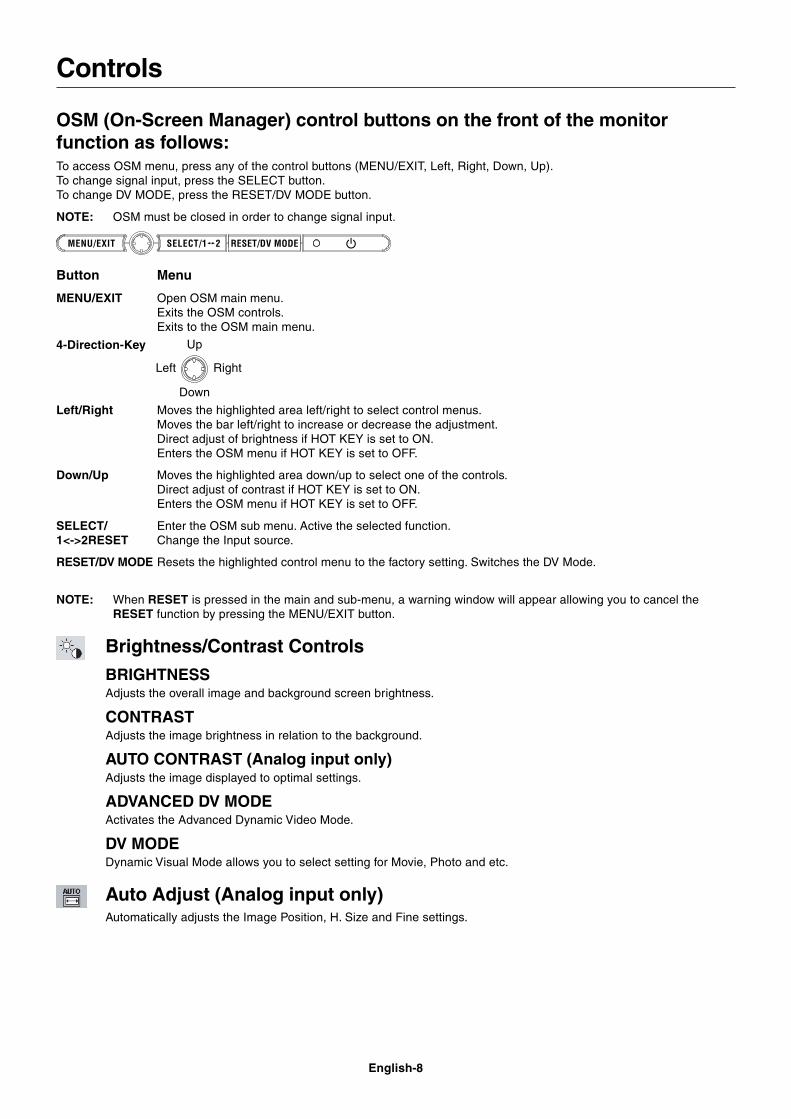
Controls
OSM (On-Screen Manager) control buttons on the front of the monitorfunction as follows:To access OSM menu, press any of the control buttons (MENU/EXIT, Left, Right, Down, Up).To change signal input, press the SELECT button.To change DV MODE, press the RESET/DV MODE button.
NOTE: OSM must be closed in order to change signal input.
NOTE: When RESET is pressed in the main and sub-menu, a warning window will appear allowing you to cancel theRESET function by pressing the MENU/EXIT button.
Brightness/Contrast ControlsBRIGHTNESSAdjusts the overall image and background screen brightness.
CONTRASTAdjusts the image brightness in relation to the background.
AUTO CONTRAST (Analog input only)Adjusts the image displayed to optimal settings.
ADVANCED DV MODEActivates the Advanced Dynamic Video Mode.
DV MODEDynamic Visual Mode allows you to select setting for Movie, Photo and etc.
Auto Adjust (Analog input only)Automatically adjusts the Image Position, H. Size and Fine settings.
Menu
Open OSM main menu.Exits the OSM controls.Exits to the OSM main menu.
Button
MENU/EXIT
Left/Right
Down/Up
SELECT/1<->2RESET
RESET/DV MODE
Moves the highlighted area left/right to select control menus.Moves the bar left/right to increase or decrease the adjustment.Direct adjust of brightness if HOT KEY is set to ON.Enters the OSM menu if HOT KEY is set to OFF.
Moves the highlighted area down/up to select one of the controls.Direct adjust of contrast if HOT KEY is set to ON.Enters the OSM menu if HOT KEY is set to OFF.
Enter the OSM sub menu. Active the selected function.Change the Input source.
Resets the highlighted control menu to the factory setting. Switches the DV Mode.
4-Direction-Key Up
Down
RightLeft

Eng
lish
English-9
Image Controls (Analog input only)
LEFT / RIGHTControls Horizontal Image Position within the display area of the LCD.
DOWN / UPControls Vertical Image Position within the display area of the LCD.
H.SIZEAdjusts the horizontal size by increasing or decreasing this setting.
FINEImproves focus, clarity and image stability by increasing or decreasing this setting.
Colour Control SystemColour Control System: Six colour presets select the desired colour setting (sRGB and NATIVE colour presets arestandard and cannot be changed).
R,G,B: Increases or decreases Red, Green or Blue colour depending upon which is selected. The change in colourwill appear on screen and the direction (increase or decrease) will be shown by the bars.
NATIVE: Original colour presented by the LCD panel that is unadjustable.
sRGB: sRGB mode dramatically improves the colour fidelity in the desktop environment by a single standard RGBcolour space. With this colour supported environment, the operator could easily and confidently communicate colourwithout further colour management overhead in the most common situations.
NOTE: When MOVIE, GAMING, or PHOTO is selected as the DV MODE, NATIVE is selected automatically as the sixcolour preset and cannot be changed.
ToolsSHARPNESS: Adjust the image to get distinct or as soft a picture as is preferred.
EXPANSION: Selects the zoom mode.FULL: The image is expanded to 1680 x 1050, regardless of the resolution.ASPECT: The image is expanded without changing the aspect ratio.OFF: The image is not expanded.NOTE: EXPANSION is available only resolution under 1280 x 1024.
OFF TIMER: Monitor will automatically power-down when the end user has selected a predetermined amount oftime.
LED BRIGHTNESS: You can adjust the Blue LED brightness.
HOT KEY: You can adjust the brightness and contrast directly. When this function is set to ON, you can adjust thebrightness with left or right control and contrast with up or down control while the OSM menu is off.
FACTORY PRESET: Selecting Factory Preset allows you to reset all OSM control settings back to the factorysettings. The RESET button will need to be held down for several seconds to take effect. Individual settings can bereset by highlighting the control to be reset and pressing the RESET button.
Menu ToolsLANGUAGE: OSM control menus are available in eight languages.
OSM LEFT/RIGHT: You can choose where you would like the OSM control image to appear horizontally on yourscreen.
OSM DOWN/UP: You can choose where you would like the OSM control image to appear vertically on your screen.
OSM Turn Off: The OSM control menu will stay on as long as it is in use. In the OSM Turn Off submenu, you canselect how long the monitor waits after the last touch of a button to shut off the OSM control menu.
OSM Lock Out: This control completely locks out access to all OSM control functions without Brightness andContrast. When attempting to activate OSM controls while in the Lock Out mode, a screen will appear indicating theOSM controls are locked out. To activate the OSM Lock Out function, press SELECT, then right control button andhold down simultaneously. To deactivate the OSM Lock Out, press SELECT, then left control button and hold downsimultaneously while in the OSM menu.
RESOLUTION NOTIFIER: This optimal resolution is 1680 x 1050. If ON is selected, a message will appear on thescreen after 30 seconds, notifying you that the resolution is not at 1680 x 1050.
English-10
InformationThe Information menu indicates the current input, display resolution, horizontal and vertical frequency, and polaritysettings of the monitor. The model and serial numbers of your monitor are also indicated.
OSM WarningOSM Warning menus disappear with Exit button.
NO SIGNAL: This function gives a warning when there is no Horizontal or Vertical Sync. After power isturned on or when there is a change of input signal, the No Signal window will appear.
RESOLUTION NOTIFIER: This function gives a warning of use with optimized resolution. After power isturned on or when there is a change of input signal or the video signal doesn’t have proper resolution, theResolution Notifier window will open. This function can be disabled in the Menu Tools.
OUT OF RANGE: When input signal is non-supported timing or the video signal doesn’t have propertiming, the Out of Range menu will appear.

Eng
lish
English-11
Recommended useSafety Precautions and Maintenance
FOR OPTIMUM PERFORMANCE, PLEASE NOTETHE FOLLOWING WHEN SETTING UP AND USING
THE MULTISYNC LCD COLOUR MONITOR:
• DO NOT OPEN THE MONITOR. There are no user serviceable parts inside and opening or removing covers may exposeyou to dangerous shock hazards or other risks. Refer all servicing to qualified service personnel.
• Do not spill any liquids into the cabinet or use your monitor near water.
• Do not insert objects of any kind into the cabinet slots, as they may touch dangerous voltage points, which can be harmfulor fatal or may cause electric shock, fire or equipment failure.
• Do not place any heavy objects on the power cord. Damage to the cord may cause shock or fire.
• Do not place this product on a sloping or unstable cart, stand or table, as the monitor may fall, causing serious damage tothe monitor.
• Do not place any objects onto the monitor and do not use the monitor outdoors.
• The inside of the fluorescent tube located within the LCD monitor contains mercury.Please follow the bylaws or rules of your municipality to dispose of the tube properly.
• Do not bend power cord.
• Do not use monitor in high temperatured, humid, dusty, or oily areas.
• Do not cover vent on monitor.
Immediately unplug your monitor from the wall outlet and refer servicing to qualified service personnel under the followingconditions:
• When the power supply cord or plug is damaged.
• If liquid has been spilled, or objects have fallen into the monitor.
• If the monitor has been exposed to rain or water.
• If the monitor has been dropped or the cabinet damaged.
• If the monitor does not operate normally by following operating instructions.
• If glass is broken, handle with care.
• If monitor or glass is broken, do not come in contact with the liquid crystal and handle with care.
• Allow adequate ventilation around the monitor so that heat can properly dissipate. Do not block ventilatedopenings or place the monitor near a radiator or other heat sources. Do not put anything on top ofmonitor.
• The power cable connector is the primary means of detaching the system from the power supply. Themonitor should be installed close to a power outlet which is easily accessible.
• Handle with care when transporting. Save packaging for transporting.
• Image Persistence: Please be aware that LCD Technology may experience a phenomenon known as Image Persistence.Image Persistence occurs when a residual or “ghost” image of a previous image remains visible on the screen. Unlike CRTmonitors, LCD monitors’ image persistence is not permanent, but constant images being displayed for a long period oftime should be avoided. To alleviate image persistence, turn off the monitor for as long as the previous image wasdisplayed. For example, if an image was on the monitor for one hour and a residual image remains, the monitor should beturned off for one hour to erase the image.NOTE: As with all personal display devices, NEC DISPLAY SOLUTIONS recommends displaying moving images andusing a moving screen saver at regular intervals whenever the screen is idle or turning off the monitor when not in use.
CAUTION
English-12
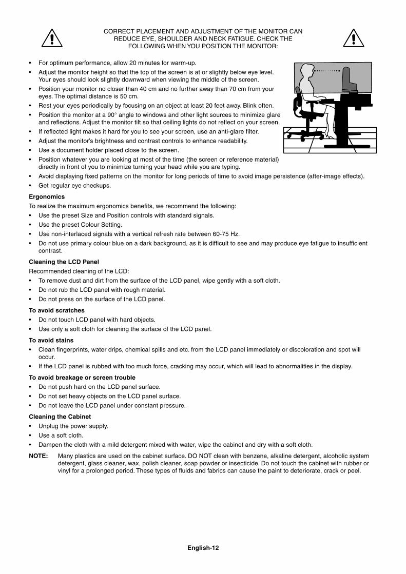
CORRECT PLACEMENT AND ADJUSTMENT OF THE MONITOR CANREDUCE EYE, SHOULDER AND NECK FATIGUE. CHECK THE
FOLLOWING WHEN YOU POSITION THE MONITOR:
• For optimum performance, allow 20 minutes for warm-up.
• Adjust the monitor height so that the top of the screen is at or slightly below eye level.Your eyes should look slightly downward when viewing the middle of the screen.
• Position your monitor no closer than 40 cm and no further away than 70 cm from youreyes. The optimal distance is 50 cm.
• Rest your eyes periodically by focusing on an object at least 20 feet away. Blink often.
• Position the monitor at a 90° angle to windows and other light sources to minimize glareand reflections. Adjust the monitor tilt so that ceiling lights do not reflect on your screen.
• If reflected light makes it hard for you to see your screen, use an anti-glare filter.
• Adjust the monitor’s brightness and contrast controls to enhance readability.
• Use a document holder placed close to the screen.
• Position whatever you are looking at most of the time (the screen or reference material)directly in front of you to minimize turning your head while you are typing.
• Avoid displaying fixed patterns on the monitor for long periods of time to avoid image persistence (after-image effects).
• Get regular eye checkups.
Ergonomics
To realize the maximum ergonomics benefits, we recommend the following:
• Use the preset Size and Position controls with standard signals.
• Use the preset Colour Setting.
• Use non-interlaced signals with a vertical refresh rate between 60-75 Hz.
• Do not use primary colour blue on a dark background, as it is difficult to see and may produce eye fatigue to insufficientcontrast.
Cleaning the LCD Panel
Recommended cleaning of the LCD:
• To remove dust and dirt from the surface of the LCD panel, wipe gently with a soft cloth.
• Do not rub the LCD panel with rough material.
• Do not press on the surface of the LCD panel.
To avoid scratches
• Do not touch LCD panel with hard objects.
• Use only a soft cloth for cleaning the surface of the LCD panel.
To avoid stains
• Clean fingerprints, water drips, chemical spills and etc. from the LCD panel immediately or discoloration and spot willoccur.
• If the LCD panel is rubbed with too much force, cracking may occur, which will lead to abnormalities in the display.
To avoid breakage or screen trouble
• Do not push hard on the LCD panel surface.
• Do not set heavy objects on the LCD panel surface.
• Do not leave the LCD panel under constant pressure.
Cleaning the Cabinet
• Unplug the power supply.
• Use a soft cloth.
• Dampen the cloth with a mild detergent mixed with water, wipe the cabinet and dry with a soft cloth.
NOTE: Many plastics are used on the cabinet surface. DO NOT clean with benzene, alkaline detergent, alcoholic systemdetergent, glass cleaner, wax, polish cleaner, soap powder or insecticide. Do not touch the cabinet with rubber orvinyl for a prolonged period. These types of fluids and fabrics can cause the paint to deteriorate, crack or peel.

Eng
lish
English-13
SpecificationsMonitor Specifications MultiSync 20WGX2 Monitor Notes
LCD Module Diagonal: 43.3 cm/20.1 inches Active matrix; thin film transistor (TFT)Viewable Image Size: 43.3 cm/20.1 inches liquid crystal display (LCD); 0.258 mm dot
Native Resolution (Pixel Count): 1680 x 1050 pitch; 470 cd/m2 white luminance; 1600:1contrast ratio, typical (in Advanced DVMode).
Input Signal Video: ANALOG 0.7 Vp-p/75 Ohms Digital Input: DVI-DSync: Separate sync.TTL Level Positive/Negative
Horizontal sync. Positive/NegativeVertical sync. Positive/NegativeComposite sync. Positive/Negative*2
Sync on Green (Video 0.7 Vp-p and Sync. Negative 0.3 Vp-p)*2
Display Colours 16,700,000 Depends on display card used.
Synchronization Range Horizontal: 31.5 kHz to 81.1 kHz AutomaticallyVertical: 56.0 Hz to 75.0 Hz Automatically
Viewing Angle Left/Right: 89°/89° (CR > 10)Up/Down: 89°/89° (CR > 10)
Resolutions Supported 720 x 400*1 at 70Hz Some systems may not support all modes640 x 480*1 at 60 Hz to 75 Hz listed.800 x 600*1 at 56 Hz to 75 Hz832 x 624*1 at 75 Hz1024 x 768*1 at 60 Hz to 75 Hz1152 x 864*1 at 75 Hz1152 x 870*1 at 75 Hz1280 x 960*1 at 60 Hz to 75 Hz1280 x 1024*1 at 60 Hz to 75 Hz1440 x 900*1 at 60 Hz Recommended resolution is 60 Hz for1680 x 1050 at 60 Hz.................................. optimal display performance.
Active Display Area Horizontal: 433.0 mm/17.0 inchesVertical: 271.0 mm/10.7 inches
USB Hub I/P: USB Specification Revision 2.0Port: Upstream 1
Downstream 4Load Current: Maximum 0.5A per port
Power Supply AC 100-240V ~ 50/60Hz
Power Consumption 84 W (typ)(without optional Sound Bar)
Current Rating 1.0 - 0.52 A
Dimensions 471.4 mm (W) x 391.5 mm (H) x 203.0 mm (D)18.6 inches (W) x 15.4 inches (H) x 8.0 inches (D)
Weight 6.3 kg (13.9 lbs)
Environmental ConsiderationsOperating Temperature: 5°C to 35°C/41°F to 95°F
Humidity: 30% to 80%Altitude: 0 to 12,000 Feet
Storage Temperature: -10°C to 60°C/14°F to 140°FHumidity: 10% to 85%Altitude: 0 to 40,000 Feet
*1 Interpolated Resolutions: When resolutions are shown that are lower than the pixel count of the LCD module, text may appear different. This isnormal and necessary for all current flat panel technologies when displaying non-native resolutions full screen. In flat panel technologies, each dot onthe screen is actually one pixel, so to expand resolutions to full screen, an interpolation of the resolution must be done.*2 If your display is not showing a picture of the SOG and Composite Sync. Signal, please contact our hotline for further assistance.
NOTE: Technical specifications are subject to change without notice.

English-14
FeaturesThin-frame design creates more desktop space for you to work and play, while the flat screen’s crisp, bright images and crystal-clear text deliver a comfortable viewing experience.
Xtra View technology allows for wide -angle viewing.
No Touch Auto Adjust automatically adjusts your optimal image settings upon initial power-on.
Colour Control System allows you to change between six colour settings on your display to match your personal preference.
Redesigned OSM controls allow you to quickly and easily adjust all elements of your screen image.
NaViSet software offers an expanded and intuitive graphical interface, allowing you to more easily adjust OSM display settingsvia mouse and keyboard.
The flat screen’s crisp, bright images and crystal-clear text deliver a comfortable viewing experience.
OptiClear LCD panel and Dynamic Visual Mode (DVM) for brilliant colour and outstanding image clarity.
ErgoDesign Features: Enhance human ergonomics to improve the working environment, protect the health of the user andsave money. Examples include OSM controls for quick and easy image adjustments, tilt base for preferred angle of vision, smallfootprint and compliance with MPRII and TCO guidelines for lower emissions.
Plug and Play: The Microsoft® solution with the Windows® 95/98/Me/2000/XP operating system facilitates setup and installationby allowing the monitor to send its capabilities (such as screen size and resolutions supported) directly to your computer,automatically optimizing display performance.
IPM (Intelligent Power Manager) System: Provides innovative power-saving methods that allow the monitor to shift to a lowerpower consumption level when on but not in use, saving two-thirds of your monitor energy costs, reducing emissions andlowering the air conditioning costs of the workplace.
Multiple Frequency Technology: Automatically adjusts monitor to the display card’s scanning frequency, thus displaying theresolution required.
FullScan Capability: Allows you to use the entire screen area in most resolutions, significantly expanding image size.
VESA Standard Mounting Interface: Allows users to connect their MultiSync monitor to any VESA standard third partymounting arm or bracket. Allows for the monitor to be mounted on a wall or an arm using any third party compliant device.
USB 2.0 hub ads excitement to your computing by connecting you to digital cameras, scanners and more.
OptiClear DVM: Provides rich colour saturation, remarkable clarity and true-to-life contrast to enhance the user’s overallvisual perception.
Eng
lish
English-15
TroubleshootingNo picture
• The signal cable should be completely connected to the display card/computer.
• The display card should be completely seated in its slot.
• Check the Vacation Switch should be in the ON position.
• Front Power Switch and computer power switch should be in the ON position.
• Check to make sure that a supported mode has been selected on the display card or system being used.(Please consult display card or system manual to change graphics mode.)
• Check the monitor and your display card with respect to compatibility and recommended settings.
• Check the signal cable connector for bent or pushed-in pins.
Power Button does not respond• Unplug the power cord of the monitor from the AC outlet to turn off and reset the monitor.
• Check the Vacation Switch on the back side of the monitor.
Image Persistence• Please be aware that LCD Technology may experience a phenomenon known as Image Persistence. Image
Persistence occurs when a residual or “ghost” image of a previous image remains visible on the screen. Unlike CRTmonitors, LCD monitors’ image persistence is not permanent, but constant images being displayed for a long period oftime should be avoided. To alleviate image persistence, turn off the monitor for as long as the previous image wasdisplayed. For example, if an image was on the monitor for one hour and a residual image remains, the monitor shouldbe turned off for one hour to erase the image.
NOTE: As with all personal display devices, NEC DISPLAY SOLUTIONS recommend displaying moving images and usinga moving screen saver at regular intervals whenever the screen is idle or turning off the monitor when not in use.
Image is unstable, unfocused or swimming is apparent• Signal cable should be completely attached to the computer.
• Use the OSM Image Adjust controls to focus and adjust display by increasing or decreasing the fine total. When thedisplay mode is changed, the OSM Image Adjust settings may need to be re-adjusted.
• Check the monitor and your display card with respect to compatibility and recommended signal timings.
• If your text is garbled, change the video mode to non-interlace and use 60Hz refresh rate.
• If you select Advanced DV mode, please select OFF.
LED on monitor is not lit (no blue or amber colour can be seen)• Power Switch should be in the ON position and power cord should be connected.
• Check the Vacation Switch should be in the ON position.
• Make sure the OSM LED Brightness Control is at the proper setting.
Display image is not sized properly• Use the OSM Image Adjust controls to increase or decrease the H. SIZE.
• Check to make sure that a supported mode has been selected on the display card or system being used.(Please consult display card or system manual to change graphics mode.)
No Video• If no video is present on the screen, turn the vacation switch off and on again.
• Make certain the computer is not in a power-saving mode (touch the keyboard or mouse).
USB Hub does not operate• Check to make sure the USB cord is properly connected. Refer to your USB device User’s manual.

English-16
TCO’03
Congratulations!The display you have just purchased carries the TCO’03 Displayslabel. This means that your display is designed, manufactured andtested according to some of the strictest quality and environmentalrequirements in the world. This makes for a high performanceproduct, designed with the user in focus that also minimizes theimpact on our natural environment.
Some of the features of the TCO’03 Display requirements:
Ergonomics• Good visual ergonomics and image quality in order to improve the working environment for
the user and to reduce sight and strain problems. Important parameters are luminance,contrast, resolution, reflectance, colour rendition and image stability.
Energy• Energy-saving mode after a certain time – beneficial both for the user and the environment• Electrical safety
Emissions• Electromagnetic fields• Noise emissions
Ecology• The product must be prepared for recycling and the manufacturer must have a certified
environmental management system such as EMAS or ISO 14 001.• Restrictions on:
- chlorinated and brominated flame retardants and polymers- heavy metals such as cadmium, mercury and lead.
The requirements included in this label have been developed by TCO Development in co-operation with scientists, experts, users as well as manufacturers all over the world. Since theend of the 1980s TCO has been involved in influencing the development of IT equipment in amore user-friendly direction. Our labelling system started with displays in 1992 and is nowrequested by users and IT-manufacturers all over the world.
For more information, please visitwww.tcodevelopment.com
Eng
lish
English-17
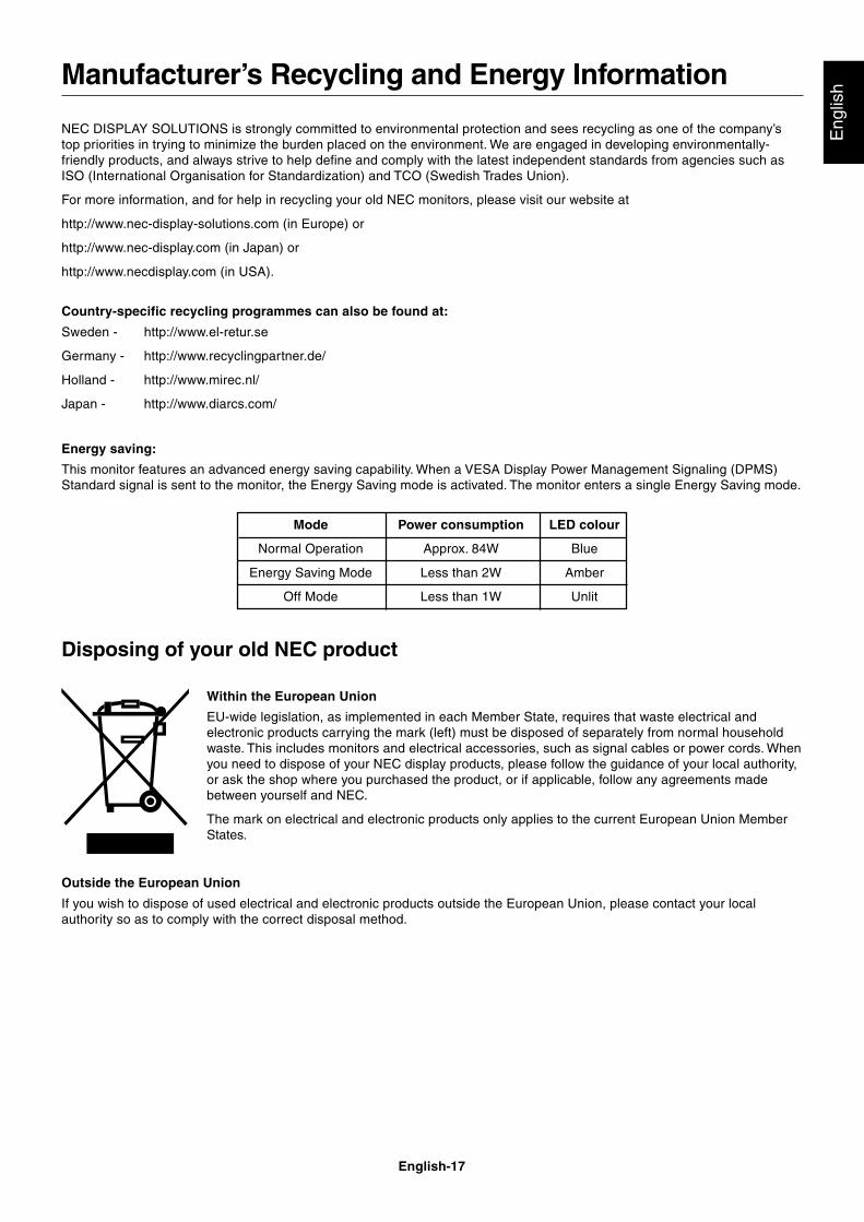
NEC DISPLAY SOLUTIONS is strongly committed to environmental protection and sees recycling as one of the company’stop priorities in trying to minimize the burden placed on the environment. We are engaged in developing environmentally-friendly products, and always strive to help define and comply with the latest independent standards from agencies such asISO (International Organisation for Standardization) and TCO (Swedish Trades Union).
For more information, and for help in recycling your old NEC monitors, please visit our website at
http://www.nec-display-solutions.com (in Europe) or
http://www.nec-display.com (in Japan) or
http://www.necdisplay.com (in USA).
Country-specific recycling programmes can also be found at:
Sweden - http://www.el-retur.se
Germany - http://www.recyclingpartner.de/
Holland - http://www.mirec.nl/
Japan - http://www.diarcs.com/
Energy saving:
This monitor features an advanced energy saving capability. When a VESA Display Power Management Signaling (DPMS)Standard signal is sent to the monitor, the Energy Saving mode is activated. The monitor enters a single Energy Saving mode.
Mode Power consumption LED colour
Normal Operation Approx. 84W Blue
Energy Saving Mode Less than 2W Amber
Off Mode Less than 1W Unlit
Manufacturer’s Recycling and Energy Information
Disposing of your old NEC product
Within the European Union
EU-wide legislation, as implemented in each Member State, requires that waste electrical andelectronic products carrying the mark (left) must be disposed of separately from normal householdwaste. This includes monitors and electrical accessories, such as signal cables or power cords. Whenyou need to dispose of your NEC display products, please follow the guidance of your local authority,or ask the shop where you purchased the product, or if applicable, follow any agreements madebetween yourself and NEC.
The mark on electrical and electronic products only applies to the current European Union MemberStates.
Outside the European Union
If you wish to dispose of used electrical and electronic products outside the European Union, please contact your localauthority so as to comply with the correct disposal method.

2-1
Serial Number InformationRefer to the serial number information shown below.
EX.) SERIAL NUMBER LABEL
g g g g g g g g g g
Manufactured Year :
(Last digit : 2005→ 5, 2006→ 6, 2007→ 7)
Manufactured Month : January to September : 1 to 9 October : X November : Y December : Z
Classification code : Discriminate by cabinet color Black : 1
Running number : Note : This running number does not reset at each month. (Example) Jan. : 00001, 00002, 00003, ….., 01234, Feb. : 01235, 01236, 01237, ….., 99999, 00001, Mar. : 00002, 00003, 00004, …..
Factory Code : G : Lite-on
Control Code: For B ver. (Europe) : B
MODEL : 20WGX2 – BK (L)
SERIAL NO. :
3- 1
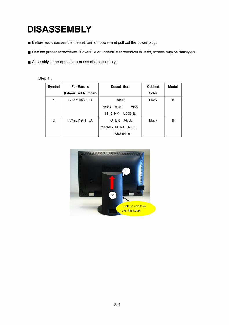
DISASSEMBLY■ Before you disassemble the set, turn off power and pull out the power plug.
■ Use the proper screwdriver. If oversize or undersize screwdriver is used, screws may be damaged.
■ Assembly is the opposite process of disassembly.
Step 1 :
1
Push up and takeover the cover
2
Symbol For Europe
(Liteon Part Number)
Description Cabinet
Color
Model
1 7737710453P0A BASE
ASSY_#6700_PC+ABS
94V0_NMV_U20BNL
Black B
2 7742611981P0A COVER_CABLE
MANAGEMENT_#6700_P
C+ABS 94V0
Black B

3- 2
Step 3 :
Step 2 :
3
Take over the terminal cover
4
Symbol ForEurope.
(Liteon Part Number)
Description Cabinet
Color
Model
3 7110340102P0A SCREW_MACHINE_NON
E_FLAT HEAD_M4_10_N
Black B
Symbol For Europe
(Liteon Part Number)
Description Cabinet
Color
Model
4 7742611931P0A COVER_TERMINAL
BOTTOM
COVER_#6700_PC+ABS
Black B

3- 3
Step 4 :
Step 5 :
5
Take off these 2 screws toremove the rear cover
Take off these 2 screws toremove the function key
6
Symbol For Europe
(Liteon Part Number)
Description Cabinet
Color
Model
6 7140226122P0A SCREW FOR CONTROL Black B
Symbol For Europe
(Liteon Part Number)
Description Cabinet
Color
Model
5 7110340102P0A SCREW_MACHINE_NON
E_FLAT HEAD_M4_10_N
Black B
3- 4
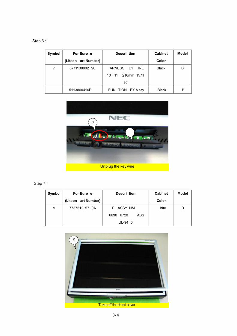
Step 7 :
Step 6 :
Symbol For Europe
(Liteon Part Number)
Description Cabinet
Color
Model
7 6711130002P90 HARNESS_KEY WIRE
_13P/11P_210mm_1571#
30
Black B
8 5113800416P FUNCTION KEY A'ssy Black B
Symbol For Europe
(Liteon Part Number)
Description Cabinet
Color
Model
9 7737512857P0A FC ASSY_NMV_
#6690/#6720_PC+ABS
UL-94V0
White B
Take off the front cover
9
7
8
Unplug the key wire

3- 5
Step 8 :
Symbol For Europe.
(Liteon Part Number)
Description Cabinet
Color
Model
10 7737609551P0A RC ASSY_KAMA 20
WS_#6700_PC+ABS
UL-94V0
Black B
10
Take off the rear cover
3- 6
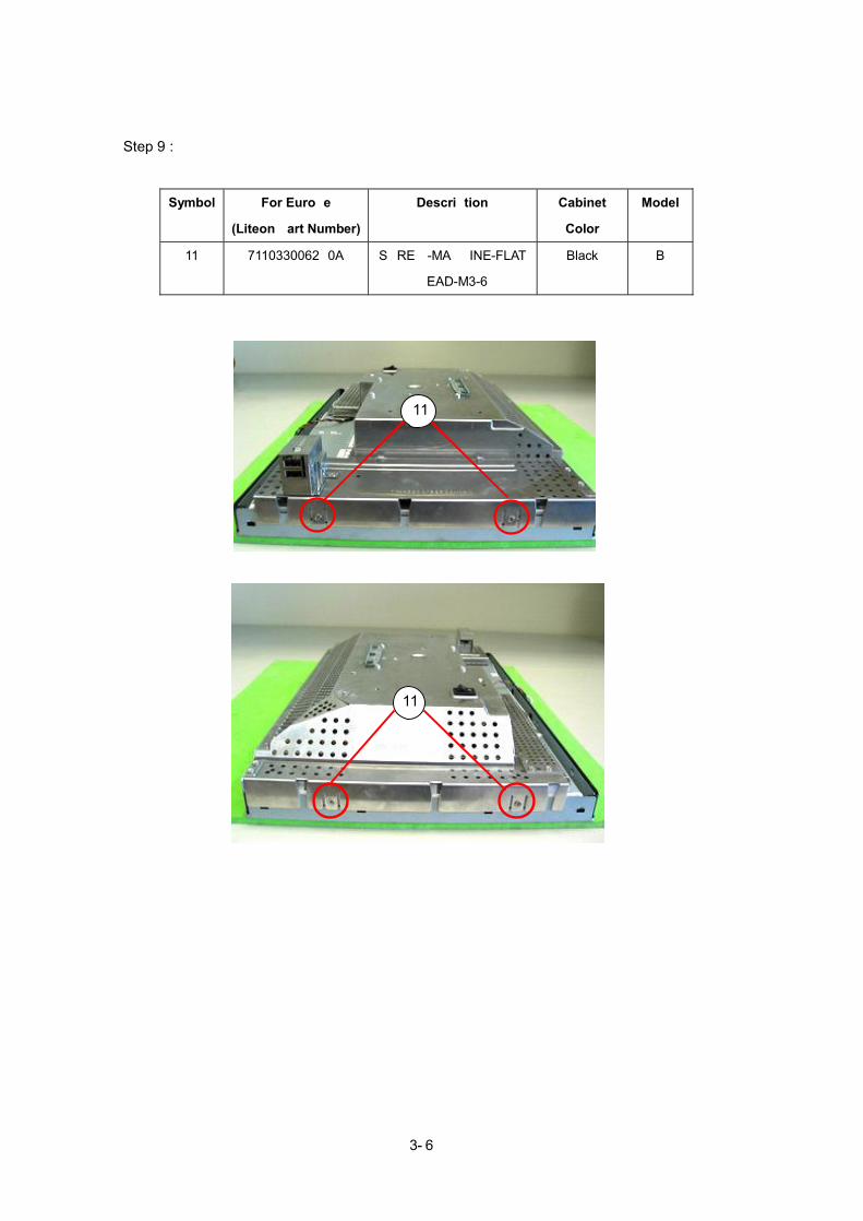
Step 9 :
11
11
Symbol For Europe
(Liteon Part Number)
Description Cabinet
Color
Model
11 7110330062P0A SCREW-MACHINE-FLAT
HEAD-M3-6
Black B
3- 7
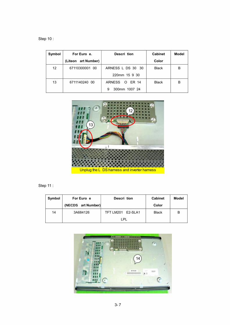
Step 10 :
Symbol For Europe.
(Liteon Part Number)
Description Cabinet
Color
Model
12 67110300001P00 HARNESS_LVDS_30P/30
P_220mm_1589#30
Black B
13 6711140240P00 HARNESS_POWER_14P/
9P_300mm_1007#24
Black B
Step 11 :
14
Symbol For Europe
(NECDS Part Number)
Description Cabinet
Color
Model
14 3A684126 TFT LM201WE2-SLA1
LPL
Black B
12
13
Unplug the LVDS harness and inverter harness
3- 8
16
15
Symbol For Europe
(Liteon Part Number)
Description Cabinet
Color
Model
15 7110630042P0A SCREW M3_4 Black B
16 7746204170P0A USB SHIELD COVER Black B
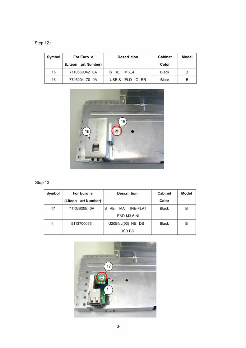
Step 12 :
Step 13 :
17
18
Symbol For Europe
(Liteon Part Number)
Description Cabinet
Color
Model
17 7110330062P0A SCREW MACHINE-FLAT
HEAD-M3-6-NI
Black B
18 5113700055P U20BNL(03)_NECDS_
USB BD
Black B

3- 9
Step 15 :
Step 14 :
19
Symbol For Europe
(Liteon Part Number)
Description Cabinet
Color
Model
19 7140330103P0A SCREW DOUBLE
THREAD FLAT M3 10L
Black B
20
Symbol For Europe
(Liteon Part Number)
Description Cabinet
Color
Model
20 7740200890P NON-STANDARD
SCREW-SCREW-CU-N
Black B

3- 10
Step 16 :
Step 17 :
21
Symbol For Europe
(Liteon Part Number)
Description Cabinet
Color
Model
21 7140330082P0A SCREW-MACHINE-NON
E-FLAT HEAD-M3-8-NI
Black B
Unplug the signal harness
3- 11
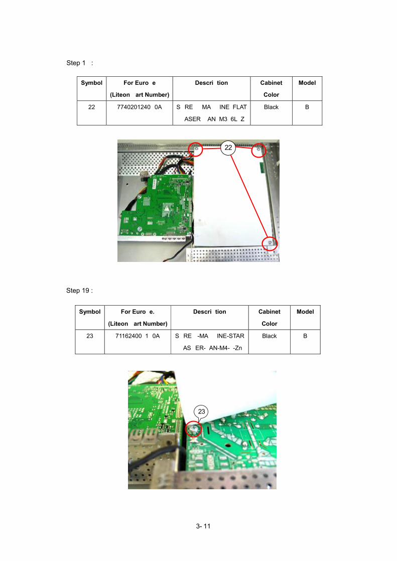
Step 18 :
Step 19 :
23
22
Symbol For Europe
(Liteon Part Number)
Description Cabinet
Color
Model
22 7740201240P0A SCREW_MACHINE_FLAT
WASER_PAN_M3_6L_Z
Black B
Symbol For Europe.
(Liteon Part Number)
Description Cabinet
Color
Model
23 7116240081P0A SCREW-MACHINE-STAR
WASHER-PAN-M4-8-Zn
Black B
3- 12
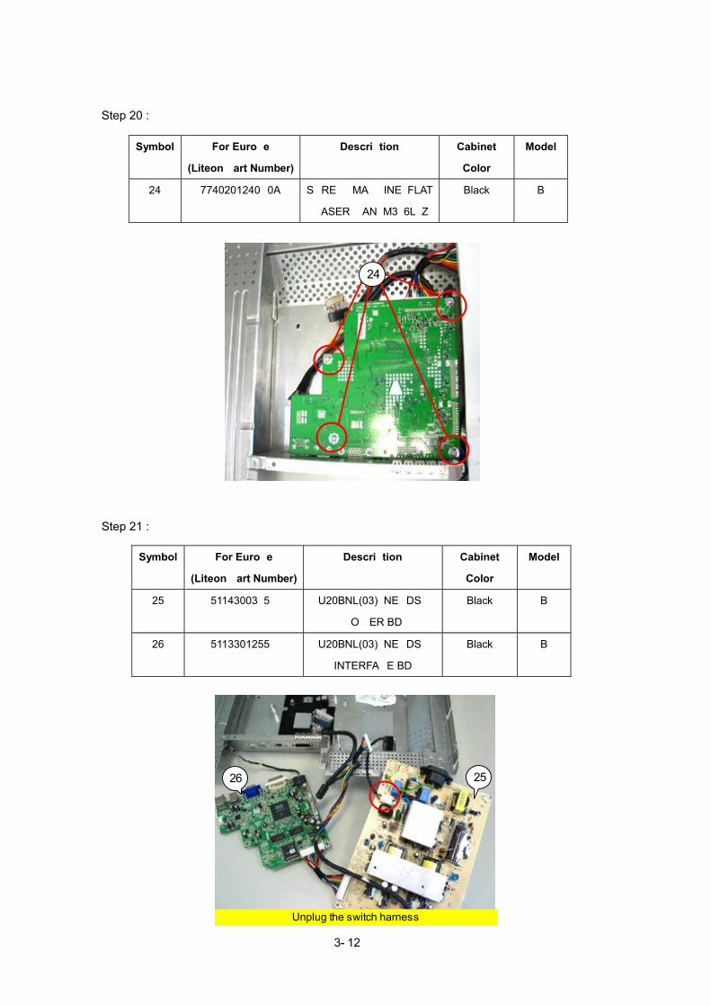
Step 20 :
24
Step 21 :
Symbol For Europe
(Liteon Part Number)
Description Cabinet
Color
Model
24 7740201240P0A SCREW_MACHINE_FLAT
WASER_PAN_M3_6L_Z
Black B
2526
Unplug the switch harness
Symbol For Europe
(Liteon Part Number)
Description Cabinet
Color
Model
25 5114300385P U20BNL(03)_NECDS_
POWER BD
Black B
26 5113301255P U20BNL(03)_NECDS_
INTERFACE BD
Black B

3- 13
Attention: Raise the reef spring to contact a metallic chassis of the LCD panel when you attach the LCDpanel to the chassis base.However, be careful, for if you pull it up too hard, the leaf spring would be detached.
Spring for EMI (Reef Spring)
Step 22 :
28
27
Symbol For Europe
(Liteon Part Number)
Description Cabinet
Color
Model
27 7746204162P0B SHIELD_SHIELD
COVER_AL ALLOY1100
T=1.0
Black B
28 6711030003P91 HARNESS_3P/SWITCH
BLK_150mm_1007#22_E
T
Black B
4- 1
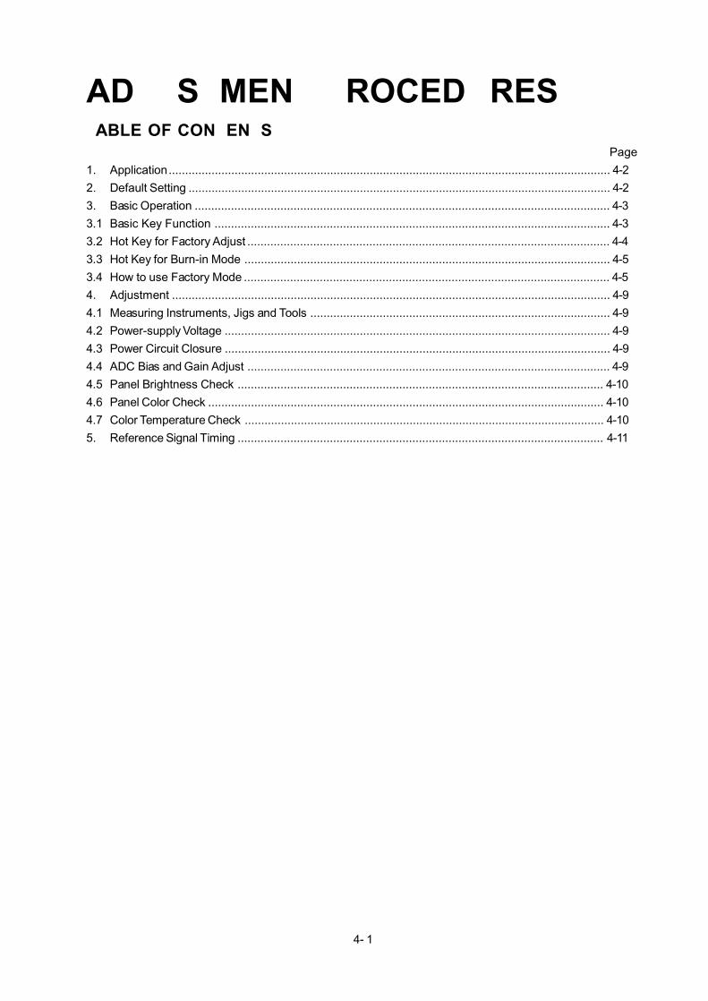
ADJUSTMENT PROCEDURESTABLE OF CONTENTS
Page
1. Application...................................................................................................................................... 4-2
2. Default Setting ................................................................................................................................ 4-2
3. Basic Operation .............................................................................................................................. 4-3
3.1 Basic Key Function ........................................................................................................................ 4-3
3.2 Hot Key for Factory Adjust .............................................................................................................. 4-4
3.3 Hot Key for Burn-in Mode ............................................................................................................... 4-5
3.4 How to use Factory Mode ............................................................................................................... 4-5
4. Adjustment ..................................................................................................................................... 4-9
4.1 Measuring Instruments, Jigs and Tools ........................................................................................... 4-9
4.2 Power-supply Voltage ..................................................................................................................... 4-9
4.3 Power Circuit Closure ..................................................................................................................... 4-9
4.4 ADC Bias and Gain Adjust .............................................................................................................. 4-9
4.5 Panel Brightness Check ............................................................................................................... 4-10
4.6 Panel Color Check ........................................................................................................................ 4-10
4.7 Color Temperature Check ............................................................................................................. 4-10
5. Reference Signal Timing ............................................................................................................... 4-11

4- 2
1. ApplicationThis adjustment specification should be applied to the 20WGX2 monitor .
2. Default Setting
Default Setting Item
Analog Digital
Volume ---
Mute ---
Brightness 100% 100%
Contrast 50% 50%
Advanced DV Mode Off Off
DV mode Standard Standard
H. Position ----
V. Position
H/V position : optimal value
for the signals, which is stated
in the VESA standard or close
value to the optimal value ----
H Size
H size : optimal value for the
signals, which is stated in the
VESA standard or close value
to the optimal value
----
FINE 0 ----
Selection of Accucolor Preset N (Native) N (Native)
OSM Left/Right Center of horizontal position
OSM Down/Up Center of vertical position
OSM Turn off time 45 (sec.)
OSM Lock out Not locked
Resolution Notifier ON
Sharpness 16.6%
Expansion Mode Full
Off Timer Off
LED Brightness 100%
Language Depend on destination
Hot Key Depend on destination OSM Select Depend on destination URL-Indication Depend on destination
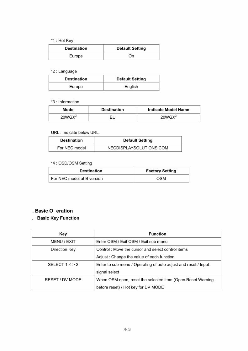
4- 3
3. Basic Operation3.1 Basic Key Function
Key Function
MENU / EXIT Enter OSM / Exit OSM / Exit sub menu
Direction Key Control : Move the cursor and select control items
Adjust : Change the value of each function
SELECT 1 <-> 2 Enter to sub menu / Operating of auto adjust and reset / Input
signal select
RESET / DV MODE When OSM open, reset the selected item (Open Reset Warning
before reset) / Hot key for DV MODE
*1 : Hot Key
Destination Default Setting
Europe On
*2 : Language
Destination Default Setting
Europe English
*3 : Information
Model Destination Indicate Model Name
20WGX2 EU 20WGX2
URL : Indicate below URL.
Destination Default Setting
For NEC model NECDISPLAYSOLUTIONS.COM
*4 : OSD/OSM Setting
Destination Factory Setting
For NEC model at B version OSM
4- 4
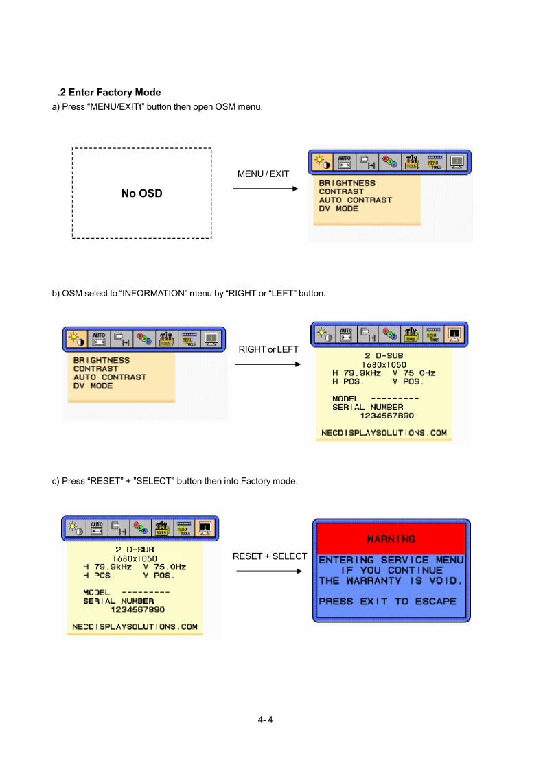
3.2 Enter Factory Modea) Press “MENU/EXITt” button then open OSM menu.
b) OSM select to “INFORMATION” menu by “RIGHT or “LEFT” button.
c) Press “RESET” + ”SELECT” button then into Factory mode.
No OSD
MENU / EXIT
RIGHT or LEFT
RESET + SELECT
1680x1050
1680x1050

4- 5
3.3 Enter Burn-in Modea) No signal input.
b) Press “RESET” + “SELECT” button then into Burn-in mode.
RESET + SELECT
3.4 How to use Factory ModePage 1
■ HOURS RUNNING
Indicate the “monitor power ON time” and “power save time” counted from factory shipment.
Hours Running function has four kinds of timer.
a. Monitor power on time (Reset-able)
b. Power save time (Reset-able)
c. Monitor power on time (Un reset-able)
d. Power save time (Un reset-able)
Note1: Power save time = Stand by mode + Suspend mode + off mode
(Do not include complete off mode.)
The default is Reset-able timers, so reset-able timers shall be shown when open the tag which includes
Hours Running function.
Indication of Reset-able and Un reset-able can be changed by key input.
“RESET” + “LEFT”: Display Reset-able timers
“RESET” + “RIGHT”: Display Un reset-able timers
When “RESET” + “LEFT” + ”SELECT” key is pressed during displaying Reset-able or Un reset-able
timers, reset the Reset-able timers to “0” and display Reset-able timers.
The Reset-able timers are reset to “0” by “Factory Preset” in factory mode.
All timers shall be counted up every 5 minutes and count up to 65535H55M after that all timers keep
65535H55M. Do not reset to 00000H00M after 65535H55M.
4- 6
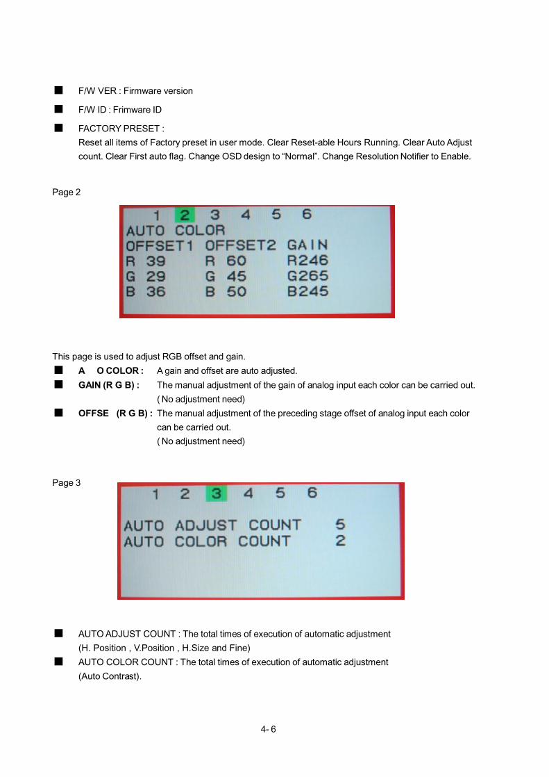
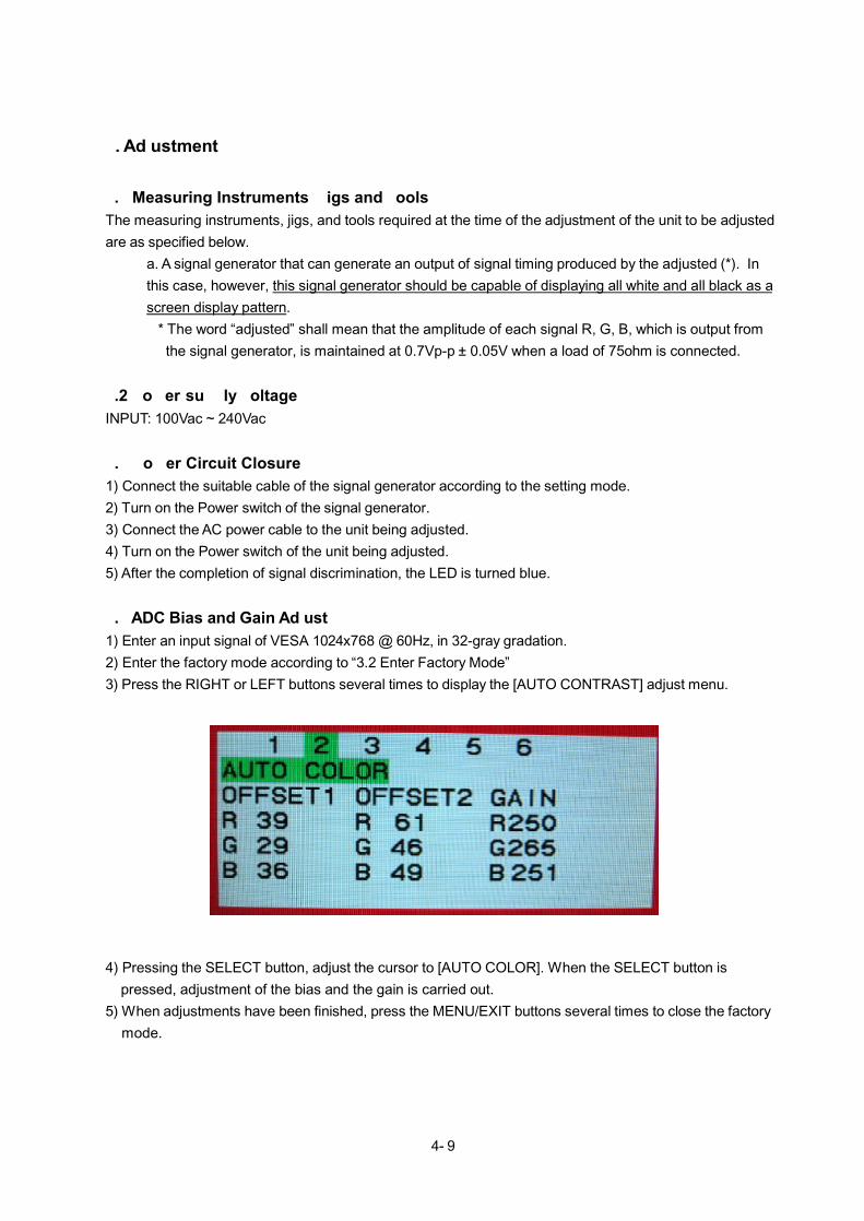
Page 2
This page is used to adjust RGB offset and gain.■ AUTO COLOR : A gain and offset are auto adjusted.■ GAIN (R/G/B) : The manual adjustment of the gain of analog input each color can be carried out.
( No adjustment need)■ OFFSET (R/G/B) : The manual adjustment of the preceding stage offset of analog input each color
can be carried out.
( No adjustment need)
Page 3
■ AUTO ADJUST COUNT : The total times of execution of automatic adjustment
(H. Position , V.Position , H.Size and Fine)■ AUTO COLOR COUNT : The total times of execution of automatic adjustment
(Auto Contrast).
■ F/W VER : Firmware version
■ F/W ID : Frimware ID
■ FACTORY PRESET :
Reset all items of Factory preset in user mode. Clear Reset-able Hours Running. Clear Auto Adjust
count. Clear First auto flag. Change OSD design to “Normal”. Change Resolution Notifier to Enable.
4- 7
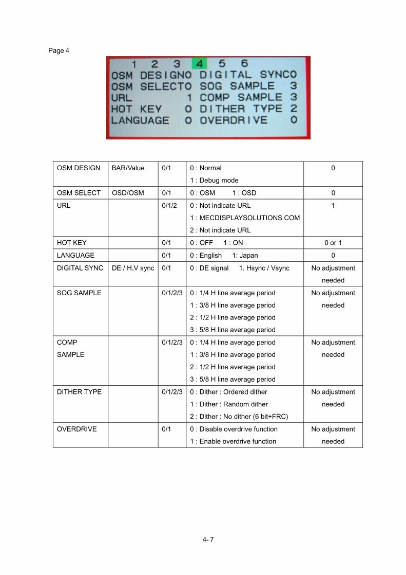
Page 4
OSM DESIGN BAR/Value 0/1 0 : Normal
1 : Debug mode
0
OSM SELECT OSD/OSM 0/1 0 : OSM 1 : OSD 0
URL 0/1/2 0 : Not indicate URL
1 : MECDISPLAYSOLUTIONS.COM
2 : Not indicate URL
1
HOT KEY 0/1 0 : OFF 1 : ON 0 or 1
LANGUAGE 0/1 0 : English 1: Japan 0
DIGITAL SYNC DE / H,V sync 0/1 0 : DE signal 1. Hsync / Vsync No adjustment
needed
SOG SAMPLE 0/1/2/3 0 : 1/4 H line average period
1 : 3/8 H line average period
2 : 1/2 H line average period
3 : 5/8 H line average period
No adjustment
needed
COMP
SAMPLE
0/1/2/3 0 : 1/4 H line average period
1 : 3/8 H line average period
2 : 1/2 H line average period
3 : 5/8 H line average period
No adjustment
needed
DITHER TYPE 0/1/2/3 0 : Dither : Ordered dither
1 : Dither : Random dither
2 : Dither : No dither (6 bit+FRC)
No adjustment
needed
OVERDRIVE 0/1 0 : Disable overdrive function
1 : Enable overdrive function
No adjustment
needed

4- 8
Page 6
■ Each Color Temperature Data. (Adjustment needed)
Page 5
■ LCD panel type.
4- 9
4. Adjustment
4.1 Measuring Instruments, Jigs and ToolsThe measuring instruments, jigs, and tools required at the time of the adjustment of the unit to be adjusted
are as specified below.
a. A signal generator that can generate an output of signal timing produced by the adjusted (*). In
this case, however, this signal generator should be capable of displaying all white and all black as a
screen display pattern.
* The word “adjusted” shall mean that the amplitude of each signal R, G, B, which is output from
the signal generator, is maintained at 0.7Vp-p ± 0.05V when a load of 75ohm is connected.
4.2 Power-supply VoltageINPUT: 100Vac ~ 240Vac
4.3 Power Circuit Closure1) Connect the suitable cable of the signal generator according to the setting mode.
2) Turn on the Power switch of the signal generator.
3) Connect the AC power cable to the unit being adjusted.
4) Turn on the Power switch of the unit being adjusted.
5) After the completion of signal discrimination, the LED is turned blue.
4.4 ADC Bias and Gain Adjust1) Enter an input signal of VESA 1024x768 @ 60Hz, in 32-gray gradation.
2) Enter the factory mode according to “3.2 Enter Factory Mode”3) Press the RIGHT or LEFT buttons several times to display the [AUTO CONTRAST] adjust menu.
4) Pressing the SELECT button, adjust the cursor to [AUTO COLOR]. When the SELECT button is
pressed, adjustment of the bias and the gain is carried out.
5) When adjustments have been finished, press the MENU/EXIT buttons several times to close the factory
mode.
4- 10
4.5 Panel Brightness Check1) Enter the input signal of 1680x1050 @ 60Hz, in Full white pattern.
2) Proceed “Factory Preset” function of tool menu.
3) OSM setting “BRIGHTNESS” to Max. (100%) and “CONTRAST” to 100%.
4) Color temperature setting to “NATIVE”.5) Check the center luminance should 250cd/m 2.
4.6 Panel Color Check1) Enter an input signal of 1680x1050 @ 60Hz, in Full white pattern.
2) Proceed “Factory Preset” function of tool menu.
3) OSM “ BRIGHTNESS” setting to Max. (100%) and “CONTRAST” setting to 50%.
4) Color temperature setting to “NATIVE”.5) Check the center color coordination.
x = 313 0.03 y = 329 0.03
4.7 Color Temperature Check1) Enter an input signal of 1680x1050 @ 60Hz, in Full white pattern.
2) OSM “BRIGHTNESS” setting to Max. (100%) and “CONTRAST” setting to 50%.
3) Color temperature setting to each color.
4) Each color temperature setting as below:
9300K: x = 0.283 0.03 y = 0.297 0.03
8200K: x = 0.292 0.03 y = 0.307 0.03
7500K: x = 0.299 0.03 y = 0.315 0.03
6500K: x = 0.313 0.03 y = 0.329 0.03
5000K: x = 0.346 0.03 y = 0.359 0.03
≧
± ±
± ±
± ±
± ±
±
±
±
±
4- 11
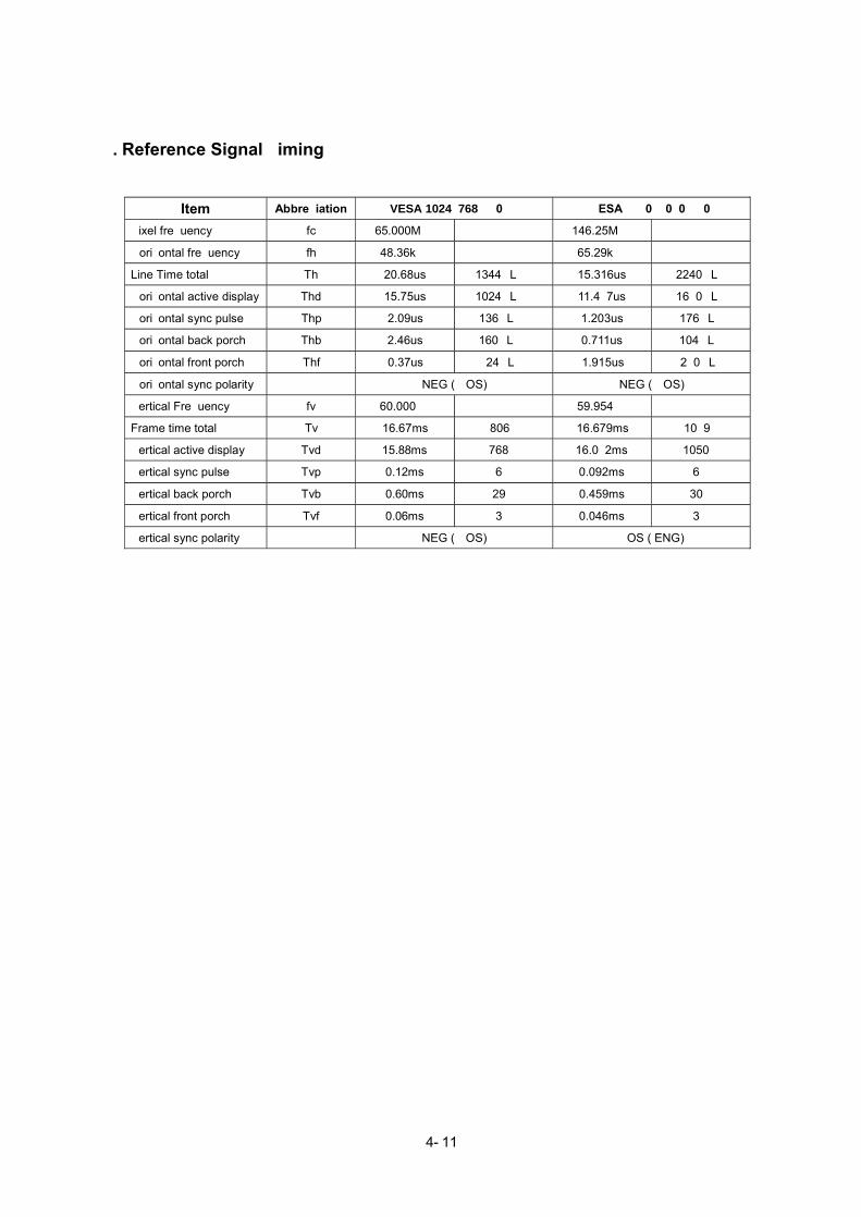
5. Reference Signal Timing
Item Abbreviation VESA 1024x768@60Hz VESA 1680x1050@60Hz
Pixel frequency fc 65.000MHz 146.25MHz
Horizontal frequency fh 48.36kHz 65.29kHz
Line Time total Th 20.68us 1344CLK 15.316us 2240CLK
Horizontal active display Thd 15.75us 1024CLK 11.487us 1680CLK
Horizontal sync pulse Thp 2.09us 136CLK 1.203us 176CLK
Horizontal back porch Thb 2.46us 160CLK 0.711us 104CLK
Horizontal front porch Thf 0.37us 24CLK 1.915us 280CLK
Horizontal sync polarity NEG (/POS) NEG (/POS)
Vertical Frequency fv 60.000Hz 59.954Hz
Frame time total Tv 16.67ms 806H 16.679ms 1089H
Vertical active display Tvd 15.88ms 768H 16.082ms 1050H
Vertical sync pulse Tvp 0.12ms 6H 0.092ms 6H
Vertical back porch Tvb 0.60ms 29H 0.459ms 30H
Vertical front porch Tvf 0.06ms 3H 0.046ms 3H
Vertical sync polarity NEG (/POS) POS (/ENG)

5-1
INSPECTIONTABLE OF CONTENTS
Page
1. General Description .......................................................................................................5-3
2. Electrical Characteristics ...............................................................................................5-4
2.1 Input Signals ..................................................................................................................5-4
2.2 Power Supply ................................................................................................................5-6
2.3 Power Management .......................................................................................................5-7
2.4 Others ...........................................................................................................................5-8
2.5 Touch Panel Capability ...................................................................................................5-9
2.6 White Color Temperature...............................................................................................5-9
2.7 Visual Ergonomic Requirement of TCO’03 Standard ...................................................5-10
2.8 Criteria for Noise* ........................................................................................................5-10
3. Connector Pin Assignment .......................................................................................... 5-11
3.1 Analog Video Input : Mini D-sub 15 pin.......................................................................... 5-11
3.2 Digital Inter Face Signals .............................................................................................5-12
4. Support Video Modes...................................................................................................5-13
5. DDC Function .............................................................................................................5-15
5.1 Plug & Play ..................................................................................................................5-15
5.2 Remote Control ...........................................................................................................5-15
6. Other Function ............................................................................................................5-15
6.1 Full Scan Capacity .......................................................................................................5-15
6.2 85Hz Refresh Rate Support ........................................................................................5-16
6.3 50Hz Refresh Rate Support ........................................................................................5-16
7. External Inspection on the LCD Module ........................................................................5-17
7.1 Inspection Condition.....................................................................................................5-17
7.2 Polarizer Defects................................................................................................................5-18
7.3 Foreign Material..................................................................................................................5-19
7.4 Line Defect..........................................................................................................................5-19
7.5 Bezel Appearance..............................................................................................................5-19
7.6 Others.................................................................................................................................5-19
5-2
Page
8. Safety ..........................................................................................................................5-20
8.1Insulation Resistance Test ..........................................................................................5-20
8.2Dielectric Strength Test .............................................................................................5-20
8.3Leakage Current Test ................................................................................................5-21
8.4Ground Continuity ......................................................................................................5-21
8.5CTI Value of PCB........................................................................................................5-21
8.6Others .........................................................................................................................5-21
9. Inspection of PLUG & PLAY Communication and OSM “MONITOR INFORMATION”for Model Name/ Serial Number Inspection .....................................................................5-22
9.1 System Connection .......................................................................................................5-22
9.2 Input Signal .....................................................................................................................5-23
9.3 Program .........................................................................................................................5-23
9.4 Operation .......................................................................................................................5-24
9.5 EDID Data File ................................................................................................................5-29
9.6 EDID Write Protect Cancel Signal Timing ......................................................................5-29
Appendix Reference Signal Timings ....................................................................................5-30

5-3
1. General Description Product Specifications
Specification Item
Analog Input Digital Input LPL LM201WE2-SLA1
Size 20.1" (51.1133cm) Active Display Area 433.44 (H) x 270.90 (V) mm Resolution 1680x1050 dots (WSXGA+) Pixel Pitch 0.258mm Color Depth 16,77 M color (8-bits) Luminance 470cd/m2(Typ.) *1)
CR>10 Up 89 / Down 89 / Left 89 / Right 89 (Typ.) Viewing Angle(Typ.) CR>5 -
Contrast Ratio 700:1(Typ.) 1600:1 (Typ.) (Advanced DV mode “ON”)
ON+OFF 12ms Response Time GTG 6ms by overdrive circuit integrated in panel
Color gamut > 72% Surface Treatment Glare (AR<2.0%)
LCD
Back Light CCFL x 10pcs (Direct Light Type) Horizontal frequency 24.7kHz - 81.2kHz 24.7kHz - 81.2kHz Vertical frequency 49.0Hz - 76.0 Hz Video Signal Analog RGB Digital RGB
Sync. Signal Separate Sync.(TTL) Composite Sync.on Green video
TMDS
Pixel Clock 25.2MHz – 165MHz
Input Signals
Input connector Mini D-sub 15Pin DVI-D Preset Timings User preset : 23
USB Hub (only AN/BNBK) USB Version 2.0 Self Powered Hub 1 upstream / 4 down stream
Front Control Menu/Exit, Direction (4 direction key), Select/1<->2, Reset/DV mode, Power (DC)
Back side Power (AC)
OSM
Brightness, Contrast, Auto contrast, Advanced DV mode, DV mode, Auto adjust, H Position, V position, H size, Fine, Color control, Sharpness, Expansion mode, Off timer, LED Brightness, Hot key, Factory preset, Language, OSM Left/Right, OSM Down/Up, OSM turn off, OSM Lock out, Resolution notifier, Monitor inf.
Functions
Remote Control VESA DDC/CI Safety UL/ cUL , TuV GS, CE, CB Report, PSB EMC FCC Class B, Canadian DOC Class B, C-tick Class B, CE VLF / ELF MPR-II, MPRIII, TCO' 03 Power Management VESA DPMS ,EPA, Energy star Ver 4.0 Tier2, GEEA label Ergonomics TUV/ERGONOMIE, TCO' 03 Plug and Play VESA DDC2B
Regulations
Others US Mercury Regulation, Windows XP/2000 Logo Temperature 5-35 degree C Environment
Condition Humidity 10-80% (without condensation) Input Voltage AC100-240V, 50 / 60Hz
Typ 84 W max (1.0 A @ 100 - 120V, 0.52 A @ 220 - 240V) Power consumption Power
saving <2.3W with USB hub model, <2W without USB hub (DPMS) <1W (DC Power Off) Meet to Energy Star Ver 4.0 Tier 2
Power Supply
Input Connector 3P IEC Type Weight with Stand Approx. 6.3 kg
without Stand Approx. 4.6 kg Net 471.4 (W) x 391.5(H) x 203.0(D) mm Dimension
Gross 570.0(W) x 518.0(H) x 262.0(D) mm VESA compatible arm mounting interface 100mmx100mm Tilt / Swivel / Rotation / Height Adjustment Up & Down 30deg to -5deg / Yes +/- 170degree / NA / NA
AC Power code 2.0m
Signal Cable 2.0m : minD-sub15pin - minD-sub15pin 2.0m: DVI-D - DVI-D
Accessories
Others User's manual, USB cable, etc. *1)60% of a mass-product should meet

5-4
2. Electrical Characteristics2.1 Input signals
2.1.1 Signals
2.1.2 Analog Input
White Level
Video Swing
Black Level
Setup Blank Level
Separate Sync Wave Form
Video signal Analog RGB / Digital RGB (TMDS)
Sync signal Separate Sync (Negative / Positive)
Composite Sync (Negative / Positive)
Sync on green : 0.3Vp-p (Negative)
Spec
min typical max
Video Analog Video 0.55V 0.70V 0.90V Impedance 75 ohm
Sync threshold
VIH 0 2.0V -- 5.0V Separate
Sync VIL 1 0V -- 0.8V
VIH 0 2.0V -- 0.5V Composite
Sync VIL 1 0V -- 0.7V
Impedance 2.2k ohm
Positive / Negative
Composite Sync on Green Video 0.15Vpp 0.3Vpp -- Impedance 2.2k ohm
Positive / Negative
Sync
Setup - 0V --
H-Sync 24.7kHz -- 81.2kHz Frequency
Range V-Sync 49Hz -- 76Hz
H-Sync 0.4usec -- -- Sync Pulse
V-Sync 2H -- (14H)
H-Sync 0.7us -- -- Back
Porch V-Sync 3H -- --
5-5
Composite Sync Type
This figure shows only positive sync waveform. Monitor should support negative sync waveform too.
2.1.3 Digital InputSignal Format : TMDS
White Level
Video Swing
Black Level
Setup Blank Level
Sync Sync Level
Sync On Green Wave Form
Hsync Type 1P Vsync Type 1P Composite Sync (Type1P) Composite Sync (Type2P) Composite Sync (Type20P) Composite Sync (Type21P) Composite Sync (Type22P) Composite Sync (Type 3P)
Spec
Minimum Typical Maximum
Dot clock 25.2MHz -- 165MHz
H-sync 31.5kHz -- 81.2kHz
Frequency
Range
V-sync 49Hz -- 76Hz
H-sync -- -- -- Sync Pulse
V-sync -- -- --
H-sync -- -- -- Back Porch
V-sync -- -- --

5-6
2.2 Power Supply
(*1) The power consumption should meet to Energy Star Ver 4.0 Tier 2.
Condition : Input Signal : Native resolution, maximum freq
Image pattern: Worst condition
Brightness: 175cd/m2 or minimum
USB Upstream: Connected
USD Downstream: No load.
Criteria: Under 50W.
kk+Inlet connector type: 3 polarity, 10A 250V 65degC
VDE, UL CSA approved CEE input connector.
EN60320 Class I standard compliant
Pin Name Definition 1 L Live 2 N Neutral 3 FG GND (Ground)
3
1 2
Input Voltage AC100 - 240V +/- 10%
Input Current (*1) 1.0 A@AC100V / 0.52 A@AC240V
Frequency 50 / 60 Hz +/-3Hz
Power Consumption 84 W (Max) with USB no load condition (*1)
AC Leakage current < 3.5mA (AC120V/240V) < 0.2mA (at AC100V with 2pin AC cable without GND)
Inrush current (cold start) < 30Arms

5-7
2.3 Power Management
This function conforms DPMS of VESA, and International Energy Star Office Equipment program.
Power Management condition and status for ANALOG Input mode
Power Management condition and status for DIGITAL Input mode
Signals Power State
Horizontal Vertical Video USB
Power Consumption (W)
Recovery Time (sec) LED status
On ON ON Active ON Refer to 3.2 --- Blue
OFF ON Blanked ON < 3sec. Orange
ON OFF Blanked ON < 3sec. Orange DPMS
OFF OFF Blanked ON
< 2.3W (Connect only USB Upstream cable, GEEA2005
Request)
< 2.0W (Not connect USB,
Energy Star Ver4.0 Tier 2)
< 3sec. Orange
DC power off
- - - OFF
< 1.0W (Connect only USB Upstream cable, GEEA2005
Request)
< 1.0W (Not connect USB,
Energy Star Ver4.0 Tier 2 Request)
< 3sec. None
AC power (Vacation SW) off
- - - - < 1W --- None
Signals Power State
DE Horizontal Vertical Video USB
Power Consumption
Recovery Times
LED status
On Pulses ON ON Active ON Refer to 3.2 --- Blue
DPMS No Pulses N/A N/A Blanked ON
< 2.3W (Connect only USB Upstream cable, GEEA2005
Request)
< 2.0W (Not connect USB,
Energy Star Ver4.0 Tier 2)
< 3 sec. Orange
DC Power off - - - - OFF
< 1.0W (Connect only USB Upstream cable, GEEA2005
Request)
< 1.0W (Not connect USB,
Energy Star Ver4.0 Tier 2 Request)
< 3 sec. None
AC power (Vacation SW) off
- - - - - < 1.0W --- None
5-8
2.4.3 USB
Self Powered Hub
Version 2.0
Downstream port : 4ports x 500mA, Connector A type
(2 ports left side of monitor. 2 ports backside of monitor.)
Up Stream port : 1port, Connector B type @ back side of monitor.
Output Voltage (Connector A) : 5.0V +/- 5%
Color of Connector : Black (PC99)
USB Hub Controller : Cypress CY7C65640A
This Hub should be meet WHQL test for Windows XP Logo and USB I/F Logo.
This function should be active at the following condition.
It is not active at the following condition for power saving.
2.4 Others
2.4.1 Scaler
NEC-DS prefers Genesis OAK chipset.
2.4.2 Audio System
None
HDCP Lead Free Faroudja Output Resolution
Gm5861 X O X WSXGA+
Condition USB Circuit
On Mode Active
PMS mode
(Windows XP, Select Screen of Property -> Select Screen saver ->
Select Monitor saving function -> Set “Turn off Monitor after XX
minutes” condition)
Active
PMS mode
(Windows XP, Select Start Menu -> Select Shut Down ->
Select Stand By mode condition)
Active
Front SW OFF (DC Power OFF) Not Active

5-9
2.4.4 Dimming Control Range
Bright ness shall be controlled by OSM less than 25% to 100%.
PWM frequency should be adjusted by MPU, and default frequency should be
3.5 times by Vsync.
.
2.5 Touch Panel Capability
None
2.5.1 Touch Panel Power Output Connector
None
2.6 White Color Temperature
White color temperature is 6 preset as 9300, 8200, 7500, sRGB (6500), 5000, Native.
Default value of user color should be Native, which is maximum setting for panel.
Target of color setting
*) TCO’03 A.2.6.1 “Color temperature variation” should follow.
sRGB should follow “Microsoft Windows Color Quality Specification for Liquid Crystal Display OEM’s”.(http://www.microsoft.com/hwdev/tech/color/ColorTest.asp)
Color Coordinate Color Coordinate Color
Temp. x y Tolerance
u’ v’ Tolerance
9300K 0.283 0.297 ±0.015 0.189 0.446 △u’v’≦0.01*
8200K 0.292 0.307 ±0.015 0.191 0.453 △u’v’≦0.01*
7500K 0.299 0.315 ±0.015 0.193 0.459 △u’v’≦0.01*
6500K
(sRGB) 0.3127 0.3291 ±0.015 0.198 0.468 △u’v’≦0.01*
5000K 0.346 0.359 ±0.015 0.209 0.488 △u’v’≦0.01*
5-10
2.7 Visual Ergonomic Requirement of TCO’03 Standard
Following items should be meet for Visual Ergonomic of TCO’03 standard.
A2.1.1 Pixel array requirement
A2.3.1 Luminance Level
A2.3.2 Luminance uniformity
A2.3.4 Luminance uniformity - angular dependence
A2.4.2 Luminance Contrast - angular dependence
A2.4.3 Luminance contrast - characters
A2.6.1 Color Temp Variation (*)
A2.6.2 Color uniformity
A2.6.3 RGB Setting
A2.6.4 Color uniformity –angular dependence
A2.6.5 Color gray scale linearity (*)
(*) Should be adjusted by monitor.
2.8 Criteria for Noise*
Any noise shall not be audible in dead room.
Noise*: Sound from inverter, power unit, or other electrical components.
Confirmation distance: 0 cm (at the every ventilation hole)

5-11
3. Connector Pin Assignment3.1 Analog Video Input: Mini D-SUB 15 PinPin assignment for analog video input connector
Pin No Signal
1 Red Video
2 Green Video / Sync on Green
3 Blue Video
4 GND
5 DDC-GND
6 Red Video GND
7 Green Video GND
8 Blue Video GND
9 +5VDC (from PC)
10 Sync. GND
11 GND
12 DDC Data (SDA)
13 Horizontal sync. / Composite Sync
14 Vertical Sync
15 DDC Clock (SCL)

5-12
3.2 Digital Inter Face SignalsPin assignment for DVI-D (24pin) connector
Pin-Assignment of DVI-D connector :
1 TX2- 9 TX1- 17 TX0+
2 TX2+ 10 TX1+ 18 TX0-
3 Shield (TX2 / TX4) 11 Shield (TX1 / TX3) 19 Shield (TX0 / TX5)
4 NC 12 NC 20 NC
5 NC 13 NC 21 NC
6 DCC-Serial Clock 14 +5V power(*) 22 Shield (TXC)
7 DCC-Serial Data 15 Ground (+5V) 23 TXC+
8 No Connect 16 Hot plug detect 24 TXC-
(*) In case, the power of the PC unit is switched off and the power of the monitor is switched on: no voltage
at pin 14.

5-13
4. Support Video ModesMonitor shall judge the received signal timing by following table.
Monitor shall support all signal timings within the following frequency range.
H-Sync range: from 24.7KHz to 81.2KHz [Analog]
H-Sync range: from 31.5KHz to 81.2KHz [Digital]
V-Sync range: from 49 Hz to 76 Hz @Dot clock : under 165MHz
V total V sync (Hz) H sync
(KHz) Type H POL V POL No. Signal Name
fV≦57.9Hz --- --- --- --- 3 640*400@56
SEP POS NEG 4 720*350@70
SEP Other Other 5 720*400@70 58.0≦fV≦77.9Hz ---
Other --- --- ---
SEP POS NEG 6 720*350@85
Out of range
SEP Other Other 7 720*400@85
Out of range
V
Total≦480
78.0Hz≦fV ---
Other --- --- ---
fV≦54.9Hz --- --- --- --- 50 640*480@50
55.0≦fV≦62.9Hz --- --- --- --- 8 640*480@60
63.0≦fV≦67.9Hz --- --- --- --- 1 640*480@66
68.0≦fV≦73.9Hz --- --- --- 9 640*480@72
74.0≦fV≦77.9Hz --- --- --- 10 640*480@75
481≦V
Total≦550
78.0Hz≦fV --- --- --- --- 11 640*480@85
Out of range
fV≦67.9Hz --- --- --- --- 35 720*576@60 551≦V
Total≦611 68.0Hz≦fV --- --- --- --- 36 720*576@75
fH≦33.0KHz --- --- --- 51 800*600@50 fV≦54.9Hz
33.1≦fH≦38.0KHz --- --- --- 46 1280*720@50
55.0≦fV≦57.9Hz --- --- --- --- 12 800*600@56
58.0≦fV≦62.9Hz --- --- --- --- 13 800*600@60
63.0≦fV≦73.9Hz --- --- --- --- 14 800*600@72
48.0≦fH≦5.09KHz --- --- --- 2 832*624@75 74.0≦fV≦77.9Hz
Other --- --- --- 15 800*600@75
612≦V
Total≦768
78.0Hz≦fV --- --- --- --- 16 800*600@85
Out of range
fV≦54.9Hz --- --- --- --- 45 1024*768@50
55.0≦fV≦62.9Hz --- --- --- --- 17 1024*768@60
--- --- --- --- --- 64 1280*768@60
63.0≦fV≦67.9Hz --- --- --- --- 29 1024*768@66
68.0≦fV≦77.9Hz --- --- --- --- 18 1024*768@70
Other --- --- --- 19 1024*768@75 73.0≦fV≦77.9Hz
63.1≦fH≦66KHz --- --- --- 44 1080*800@76
769≦V
Total≦864
78.0≦fV -- --- --- --- 20 1024*768@85
Out of range
fV≦72.9Hz -- --- --- --- 30 1152*864@70
fH≦67.9KHz --- --- --- 21 1152*864@75 73.0≦fV≦77.9Hz
Other --- --- --- 28 1152*870@75 865≦V
Total≦920
78.0≦fV -- --- --- --- 31 1152*864@85
Out of range

5-14
V total V sync (Hz) H sync
(KHz) Type H POL V POL No. Signal Name
921≦V
Total≦929 fV≦62.9Hz --- --- --- --- 52
1440*900@60
Reduced Blanking
fV≦62.9Hz --- --- --- --- 53 1440*900@60
63.0≦fV≦67.9Hz --- --- --- 22 1152*900@66
68.0≦fV≦77.9Hz --- --- --- 54 1440*900@75
Out of range
930≦V
Total≦960
78.0Hz≦fV --- --- --- --- 55 1440*900@85
Out of range
fV≦54.9Hz --- --- --- --- 47 1280*960@50
55.0≦fV≦67.9Hz --- --- --- --- 23 1280*960@60
68.0≦fV≦77.9Hz --- --- --- --- 32 1280*960@75 961≦V
Total≦1024
78.0Hz≦fV --- --- --- --- 37
1280*960@85
Out of range fV≦54.9Hz --- --- --- --- 48 1280*1024@50
55.0≦fV≦62.9Hz --- --- --- --- 24 1280*1024@60 63.0≦fV≦72.9Hz --- --- --- --- 25 1280*1024@66
fH≦80.6KHz --- --- --- 26 1280*1024@75 73.0Hz≦fV≦77.9Hz
80.7≦fH≦85.0KHz --- --- --- 27 1280*1024@76
1025≦V
Total≦1076
78.0Hz≦fV --- --- --- --- 38 1280*1024@85
Out of range 1077≦V
Total≦1083 fV≦62.9Hz --- --- --- --- 60
1680*1050@60
Reduced Blanking
fV≦62.9Hz --- --- --- --- 61 1680*1050@60
63.0≦fV≦77.9Hz --- --- --- --- 58 1400*1050@75
Out of range 1084≦V
Total≦1200
78.0≦fV --- --- --- --- 59 1400*1050@85
Out of range
fV≦54.9Hz --- --- --- --- 49 1600*1200@50
Out of range
55.0≦fV≦62.9Hz --- --- --- --- 33 1600*1200@60
Out of range 12017≦V
Total≦1300
63.0Hz≦fV --- --- --- --- 34 1600*1200@65
Out of range 1301≦V Total --- --- --- --- Out of range

5-15
5. DDC Function
5.1 Plug & PlayThis monitor abides by VESA DDC2B.
See page 5-29 for EDID data.
Monitor can output EDID data, although PC+5V from PC is inactive.
5.2 Remote ControlThis monitor abides by VESA DDC/CI.
6. Other Function
6.1 Full Scan CapacityIn case the input video mode is not native resolution, the image area shall be expanded to native resolu-
tion smoothly with the function of scaling engine.
Standard resolution : 1680x1050
Expand method : Full expand mode with smoothing as follows
Down scaling : Down scaling at over 1680x1050 mode.
Picture Size (In Full-Screen mode) Multi-pixel mode Input display Expanded Rate Expanded
Resolution Horizontal Vertical Resolution Expansion 720×350 2.33 3 1680×1050 Expansion 640×350 2.62 3 1680×1050 Expansion 640×400 2.62 2.62 1680×1050 Expansion 720×400 2.33 2.62 1680×1050 Expansion 640×480 2.62 2.18 1680×1050 Expansion 800×600 2.1 1.75 1680×1050 Expansion 832×624 2.02 1.68 1680×1050 Expansion 1024×768 1.64 1.36 1680×1050 Expansion 1152×864 1.45 1.21 1680×1050 Expansion 1152×870 1.45 1.20 1680×1050 Expansion 1152×900 1.45 1.16 1680×1050 Expansion 1280×768 1.31 1.36 1680×1050 Expansion 1280×960 1.31 1.09 1680×1050 Expansion 1360×768 1.23 1.36 1680×1050 Expansion 1400×900 1.2 1.16 1680×1050 Expansion 1400×1050 1.2 1.0 1680×1050 Standard 1680×1050 1.0 1.0 1680×1050
5-16
6.2 85Hz Refresh Rate SupportMonitor should display 85Hz refresh rate mode as emergency mode.
Monitor should display “Out of Range” warning menu at this mode.
6.3 50Hz Refresh Rate SupportIn 50Hz refresh rate signal (Following signals), the display should be smooth at “Moving character”. Itshould be taken care of the influence by “Frame buffer mode”.1) PAL signal 1
2) PAL signal 2
3) GTF 1024x768@50Hz
4) GTF1280x720@50Hz
5) GTF1280x960@50Hz
5-17
7. External Inspection on the LCD Module
7.1 Inspection Condition
7.1.1 Conditions
Ambient conditions :
a. Temperature : 20~25oC
b. Humidity : 65 +/- 5 % RH
c. Illumination : Single 20W fluorescent lamp non-directive
(Appearance - 300 to 700 Lux , Display – 180 to 200 Lux)
Viewing distance :
The distance between the LCM and the inspector’s eyes shall be at least 35cm.
Viewing Angle :
The inspection shall be conducted within normal viewing angle range.
(Refer to the CAS for viewing angle)
7.1.2 Dot Defect
7.1.2.1 Bright Dot
Dots (sub-pixels) which appeared brightly in the screen when the LCM displayed with dark
pattern.
-R,G or B 1 dot ----------------------------------------- 2 Max (BDF 95%)
-Adjacent 2 dots --------------------------------------- 0 Max
-Adjacent 3 dots --------------------------------------- 0 Max
-Total amount of Bright dots ----------------------- 2 Max
-Bright dot density ------------------------------------- Within Φ10 mm
* Small bright dot which can be seen on 64 gray pattern is to be counted asone small bright
dot defect. (Max N≦3 within 10mm*10mm, Total Max N≦8) Size of small bright dot (1/20
<R,G,B≦ 1/2)
7.1.2.2 Dark Dot
Dots(sub-pixels) which appeared darkly in the screen when the LCM displayed with bright
pattern.
-R,G or B 1 dot ------------------------------------------ 5 Max
-Adjacent 2 dots ---------------------------------------- 2 Max
-Adjacent 3 dots ---------------------------------------- 0 Max
-Total amount of Dark dot ---------------------------- 6 Max
-Dark dot density --------------------------------------- Within Φ10 mm
7.1.2.3 Total amount of Dot Defects ---------------------------- 8 Max (Combination)
Note) a. Every dot herein means Sub-Pixel. (Each Red,Green, or Blue Color)
b. Damaged less than half size of sub-pixel is not counted as defect.
c. Dots darker than half brightness of sub-pixel are not defined as bright dot defectand dots brighter
than half brightness of sub-pixel is not defined as dark dot defect.
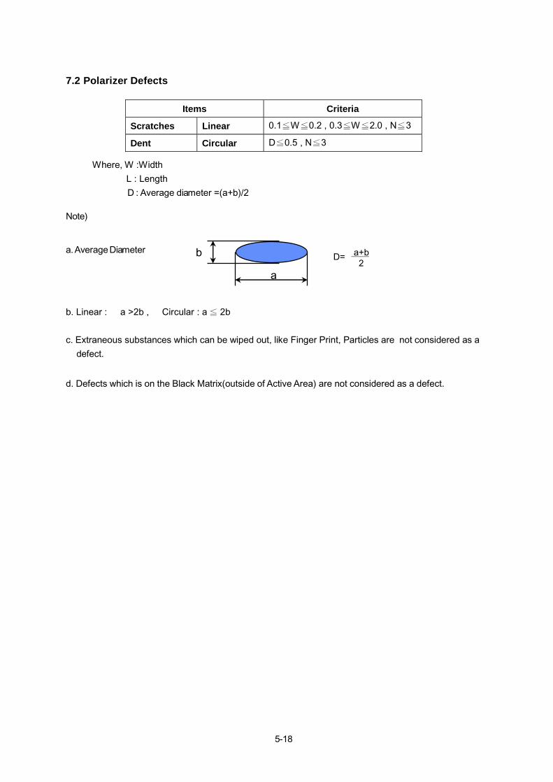
5-18
7.2 Polarizer Defects
Note)
a. Average Diameter
a
b D= a+b 2
b. Linear : a >2b , Circular : a≦ 2b
c. Extraneous substances which can be wiped out, like Finger Print, Particles are not considered as a
defect.
d. Defects which is on the Black Matrix(outside of Active Area) are not considered as a defect.
Items Criteria
Scratches Linear 0.1≦W≦0.2 , 0.3≦W≦2.0 , N≦3
Dent Circular D≦0.5 , N≦3
Where, W :Width
L : Length
D : Average diameter =(a+b)/2
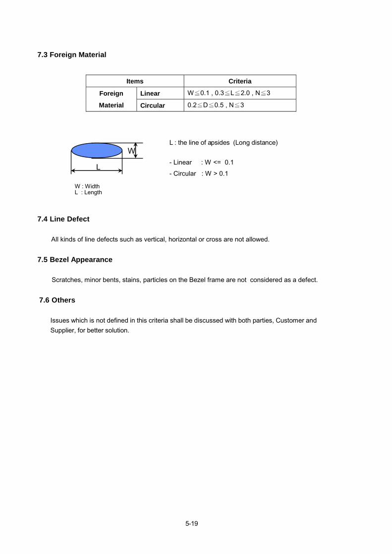
5-19
7.3 Foreign Material
L
WL : the line of apsides (Long distance)
- Linear : W <= 0.1
- Circular : W > 0.1
W : Width L : Length
7.4 Line Defect
All kinds of line defects such as vertical, horizontal or cross are not allowed.
7.5 Bezel Appearance
Scratches, minor bents, stains, particles on the Bezel frame are not considered as a defect.
7.6 Others
Issues which is not defined in this criteria shall be discussed with both parties, Customer and
Supplier, for better solution.
Items Criteria
Linear W≦0.1 , 0.3≦L≦2.0 , N≦3 Foreign
Material Circular 0.2≦D≦0.5 , N≦3

5-20
8. Safety
Destination : All over the world
Applicable standards : UL60950/C-UL/EN60950
Unit class : Class I units (the units protected against electric shocks by protective grounding, or those
equipped with 3-core power cords)
Ratings : AC100 - 240V 50/60Hz 1.3-0.7A
●
●
●
●
8.1 Insulation Resistance TestAn insulation resistance should be measured under the conditions specified below, in order to confirm
that the requirements of the judgment standard are met.
1) Measuring conditions
Measuring instrument : 500V DC MEGOHM Meter
Testing point : Between the power circuit block and the exposed metallic block
(D-SUB connector)
Measured value readout : A test voltage should be applied for one minute and the resistance
value should be read out thereafter.
2) Judgment standard:
The resistance of the insulation between the power terminal and the ground contact is more
than 10M ohms while withstanding a voltage of 500Vdc.
8.2 Dielectric Strength TestTo confirm the freedom from insulation breakdown, testing should be carried out under the conditions
specified below.
1) Measuring conditions
Measuring instrument: Dielectric strength tester (The specified voltage should be maintained in the
state that a current of 10mA is carried.)
Testing point: Between the electrical circuit block and the exposed metallic block (D-SUB
connector)
Note : The electrical circuit block should mean the power input block (primary side). Testing should
be carried out under the condition that both poles of the power plug are short-circuited. (Where
a 3-core cord is used, the two poles other than the ground terminal should be short-circuited.)
2) Judgment standard
There is no breakdown of the insulators or short circuits when applying an alternating potential of
1000Vac for a duration of 1(one) minute or 1500Vac for a duration of 2(two) second at 50Hz
between the metallic chassis and the input power supply active and neutral terminals connected
together.
●
●
●
●
●
5-21
8.3 Leakage Current TestA leakage current should be measured under the conditions specified below, in order to confirm that
the requirements of the judgment standard are met.
1) Measuring conditions
Measuring instrument : Leakage current meter (A 1500 resistor should be incorporated,
together with a bypass capacitor of 0.15 F.)
Testing point : Between the exposed metallic block (D-SUB connector) and Phases A and B of the
power source.
Condition of the set : A power cable should be connected. The see-saw switch on the set side
should be turned ON and OFF.
2) Judgment standard
The current conducted between each of the power supply’s contacts is less than 3.5mA at 255Vac
(60Hz) and 0.2mA at 100Vac(60Hz).
8.4 Ground ContinuityThe resistance between the ground side of the power cord and the accessible metal parts located in
ground circuit shall not exceed 0.1 ohm at current load of 25mA.
8.5 CTI Value of PCBCTI value of below PCB should be more than 600.
Inverter circuit.
Power supply circuit.
8.6 OthersVESA Display Data Channel Command Interface (DDC CI) Standard.
VESA Display Data Channel Command Interface – Proposed Implementation Guide.
USB Version 2.0.
USB I/F Logo.
Microsoft WHQL, Microsoft Windows XP logo.
Microsoft Windows Color Quality Specification for Liquid Crystal Display OEM’s.
Ω
μ
●
●
●

5-22
9. PLUG & PLAY Communication and OSM “MONITOR INFORMATION” for Model
Name / Serial Number Inspection
9.1 System Connection This system should be connected as shown below.
Fig 9.1.1 D-SUB connector connection
Fig 9.1.2 DVI connector connection
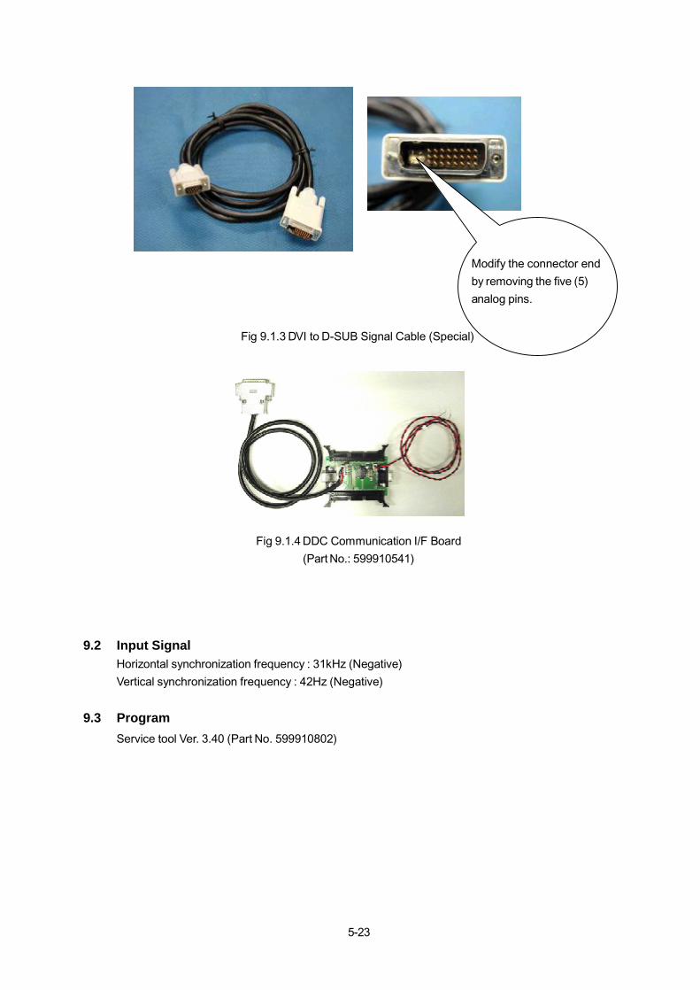
5-23
Fig 9.1.3 DVI to D-SUB Signal Cable (Special)
Fig 9.1.4 DDC Communication I/F Board
(Part No.: 599910541)
9.2 Input SignalHorizontal synchronization frequency : 31kHz (Negative)
Vertical synchronization frequency : 42Hz (Negative)
9.3 Program
Service tool Ver. 3.40 (Part No. 599910802)
Modify the connector end by removing the five (5) analog pins.
Modify the connector end
by removing the five (5)
analog pins.

5-24
9.4 Operation
9.4.1 EDID Data Inspection and Writing to the D-SUB Connector (Analog)
1) Connect the EDID data writing unit.
2) Create a unique directory in the PC, and copy all the files of service tool (Ver. 3.40) into that directory.
3) Start the service tool with file [Service2.EXE].
4) When the screen as shown below appears, click the [LCD] button of [Monitor Type] and press the
[START] button.

5-25
5) When the screen (as shown below), move the cursor to [20WGX2 D-SUB] and double click.
6) When the screen as shown below appears, select [EDID_READ] and press the [OK] button.
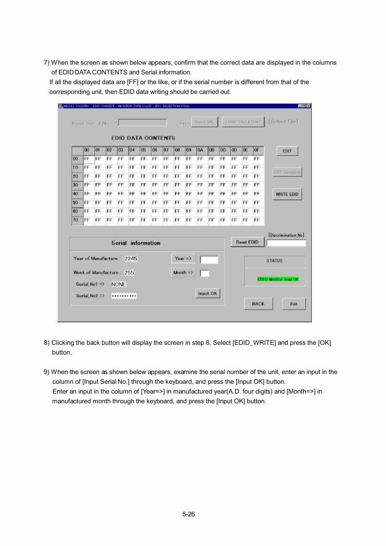
5-26
7) When the screen as shown below appears, confirm that the correct data are displayed in the columns
of EDID DATA CONTENTS and Serial information.
If all the displayed data are [FF] or the like, or if the serial number is different from that of the
corresponding unit, then EDID data writing should be carried out.
8) Clicking the back button will display the screen in step 6. Select [EDID_WRITE] and press the [OK]
button.
9) When the screen as shown below appears, examine the serial number of the unit, enter an input in the
column of [Input Serial No.] through the keyboard, and press the [Input OK] button.
Enter an input in the column of [Year=>] in manufactured year(A.D. four digits) and [Month=>] in
manufactured month through the keyboard, and press the [Input OK] button.
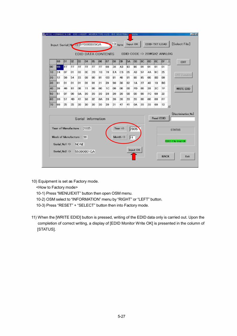
5-27
10) Equipment is set as Factory mode.
<How to Factory mode>
10-1) Press “MENU/EXIT” button then open OSM menu.
10-2) OSM select to “INFORMATION” menu by “RIGHT” or “LEFT” button.
10-3) Press “RESET” + “SELECT” button then into Factory mode.
11) When the [WRITE EDID] button is pressed, writing of the EDID data only is carried out. Upon the
completion of correct writing, a display of [EDID Monitor Write OK] is presented in the column of
[STATUS].

5-28
12) Display “MONITOR INFORMATION” of the OSM, and confirm that the model name (20WGX2) and
serial number have been correctly written. (Check that it is also in agreement with the written-in serial
number.) Model name and Serial number writing for the OSM “MONITOR INFORMATION”.
9.4.2 EDID Data Inspection and Writing to the DVI-PC Connector
1) Connect the EDID data writing unit with jigs, etc. (Refer to a DVI connector connection figure)
2) The “BACK” button is pushed twice and the [MODEL SELECT] screen is displayed. Cursor is united
and double-clicked to [20WGX2 DVI-D].
3) 6) to 11) is carried out in the procedure of the 9.4.1 “EDID data inspection and writing of a D-SUB
connector”.
4) Upon the normal completion of EDID data writing, press the [Exit] button to close the program.
5-29
9.5 EDID Data File
Note 1: address 10h Week of manufacture
Note 2: address 11h Year of manufacture - 1990
Note 3: address 71h ~ 7Dh Serial Number (ASCII coded)
If less than 13 char, terminate with 0Ah and fill the rests with 20h.
Note 4: address 7Fh Checksum
The sum of entire 128 byte should be equal to 00h.
9.6 EDID Write Protect Cancel Signal Timing
EDID Data: 20WGX2_A.edi (ANALOG)
0 1 2 3 4 5 6 7 8 9 A B C D E F
00 00 FF FF FF FF FF FF 00 38 A3 98 66 01 01 01 01
10 Note1 Note2 01 03 0E 2B 1B 78 EA C5 05 A3 57 4A 9C 25
20 12 50 54 BF EF 80 71 4F 81 CF 81 4F 81 80 95 00
30 90 40 B3 00 01 01 21 39 90 30 62 1A 27 40 18 B0
40 36 40 B1 0E 11 00 00 1C 00 00 00 FD 00 38 4B 1F
50 53 11 00 0A 20 20 20 20 20 20 00 00 00 FC 00 32
60 30 57 47 58 32 0A 20 20 20 20 20 20 00 00 00 FF
70 00 Note3 Note3 Note3 Note3 Note3 Note3 Note3 Note3 Note3 Note3 Note3 Note3 Note3 00 Note4
EDID Data: 20WGX2_D.edi (DIGITAL)
0 1 2 3 4 5 6 7 8 9 A B C D E F
00 00 FF FF FF FF FF FF 00 38 A3 99 66 01 01 01 01
10 Note1 Note2 01 03 80 2B 1B 78 EA C5 05 A3 57 4A 9C 25
20 12 50 54 BF EF 80 71 4F 81 CF 81 4F 81 80 95 00
30 90 40 B3 00 01 01 21 39 90 30 62 1A 27 40 18 B0
40 36 40 B1 0E 11 00 00 1C 00 00 00 FD 00 38 4B 1F
50 53 11 00 0A 20 20 20 20 20 20 00 00 00 FC 00 32
60 30 57 47 58 32 0A 20 20 20 20 20 20 00 00 00 FF
70 00 Note3 Note3 Note3 Note3 Note3 Note3 Note3 Note3 Note3 Note3 Note3 Note3 Note3 00 Note4
Item Abbreviation EDID write protect cancel
Pixel frequency fc 28.32MHz
Horizontal frequency fh 31.469kHz
Line Time total Th 31.777us 900CLK
Horizontal active display Thd 25.422us 720CLK
Horizontal sync pulse Thp 3.813us 108CLK
Horizontal back porch Thb 1.907us 54CLK
Horizontal front porch Thf 0.636us 18CLK
Horizontal sync polarity NEG
Vertical Frequency fv 42.015Hz
Frame time total Tv 23.801ms 749H
Vertical active display Tvd 21.768ms 685H
Vertical sync pulse Tvp 0.095ms 3H
Vertical back porch Tvb 1.494ms 47H
Vertical front porch Tvf 0.445ms 14H
Vertical sync polarity NEG
5-30
Appendix Reference Signal Timings
H-
Horizontal
H pluse H back
H total
H front
H active
V-Video
Vertical
V pluse V back
V total
V front
V active

5-31
MODE MODE
No. 1 2
Item Abbreviation MAC 640×480 MAC 832×624
Pixel frequency fc 30.24MHz 57.28MHz
Horizontal frequency fh 35.00kHz 49.73kHz
Line Time total Th 28.57us 864CLK 20.11us 1152CLK
Horizontal active display Thd 21.16us 640CLK 14.52us 832CLK
Horizontal sync pulse Thp 2.12us 64CLK 1.12us 64CLK
Horizontal back porch Thb 3.17us 96CLK 3.91us 224CLK
Horizontal front porch Thf 2.12us 64CLK 0.56us 32CLK
Horizontal sync polarity NEG (/POS) NEG (/POS)
Vertical Frequency fv 66.66Hz 74.55Hz
Frame time total Tv 15.00ms 525H 13.41ms 667H
Vertical active display Tvd 13.71ms 480H 12.55ms 624H
Vertical sync pulse Tvp 0.09ms 3H 0.06ms 3H
Vertical back porch Tvb 1.11ms 39H 0.78ms 39H
Vertical front porch Tvf 0.09ms 3H 0.02ms 1H
Vertical sync polarity NEG (/POS) NEG (/POS)
MODE MODE No. 3 4
Item Abbreviation PC98 640×400 (24.8kHz) VGA 720×350 70Hz
Pixel frequency fc 21.053MHz 28.322MHz
Horizontal frequency fh 24.83kHz 31.47kHz
Line Time total Th 40.274us 848CLK 31.78us 900CLK
Horizontal active display Thd 30.400us 640CLK 25.42us 720CLK
Horizontal sync pulse Thp 3.04us 64CLK 3.81us 108CLK
Horizontal back porch Thb 4.04us 85CLK 1.91us 54CLK
Horizontal front porch Thf 2.80us 59CLK 0.64us 18CLK
Horizontal sync polarity NEG (/POS) POS
Vertical Frequency fv 56.432Hz 70.087Hz
Frame time total Tv 17.72ms 440H 14.27ms 449H
Vertical active display Tvd 16.11ms 400H 11.12ms 350H
Vertical sync pulse Tvp 0.32ms 8H 0.06ms 2H
Vertical back porch Tvb 1.01ms 25H 1.91ms 60H
Vertical front porch Tvf 0.28ms 7H 1.18ms 37H
Vertical sync polarity NEG (/POS) NEG
5-32
MODE MODE No. 5 6
Item Abbreviation VGA 720×400 70Hz VGA 640×480 60Hz
Pixel frequency fc 28.322MHz 25.175MHz
Horizontal frequency fh 31.47kHz 31.47kHz
Line Time total Th 31.78us 900CLK 31.78us 800CLK
Horizontal active display Thd 25.42us 720CLK 25.42us 640CLK
Horizontal sync pulse Thp 3.81us 108CLK 3.81us 96CLK
Horizontal back porch Thb 1.91us 54CLK 1.91us 48CLK
Horizontal front porch Thf 0.63us 18CLK 0.64us 16CLK
Horizontal sync polarity NEG NEG (/POS)
Vertical Frequency fv 70.087Hz 59.992Hz
Frame time total Tv 14.27ms 449H 16.68ms 525H
Vertical active display Tvd 12.71ms 400H 15.25ms 480H
Vertical sync pulse Tvp 0.06ms 2H 0.06ms 2H
Vertical back porch Tvb 1.11ms 35H 1.02ms 33H
Vertical front porch Tvf 0.38ms 12H 0.35ms 10H
Vertical sync polarity POS NEG (/POS)
MODE MODE No. 7 8
Item Abbreviation VGA 640×480 72Hz VESA 640×480 75Hz
Pixel frequency fc 31.500MHz 31.500MHz
Horizontal frequency fh 37.86kHz 37.50kHz
Line Time total Th 26.41us 832CLK 26.67us 840CLK
Horizontal active display Thd 20.32us 640CLK 20.32us 640CLK
Horizontal sync pulse Thp 1.27us 40CLK 2.03us 64CLK
Horizontal back porch Thb 4.06us 128CLK 3.81us 120CLK
Horizontal front porch Thf 0.76us 24CLK 0.51us 16CLK
Horizontal sync polarity NEG (/POS) NEG (/POS)
Vertical Frequency fv 72.81Hz 75.00Hz
Frame time total Tv 13.73ms 520H 13.33ms 500H
Vertical active display Tvd 12.68ms 480H 12.80ms 480H
Vertical sync pulse Tvp 0.08ms 3H 0.08ms 3H
Vertical back porch Tvb 0.74ms 28H 0.43ms 16H
Vertical front porch Tvf 0.24ms 9H 0.03ms 1H
Vertical sync polarity NEG (/POS) NEG (/POS)
5-33
MODE MODE No. 9 10
Item Abbreviation VESA 800×600 56Hz VESA 800×600 60Hz
Pixel frequency fc 36.00MHz 40.00MHz
Horizontal frequency fh 35.16kHz 37.88kHz
Line Time total Th 28.44us 1024CLK 26.40us 1056CLK
Horizontal active display Thd 22.22us 800CLK 20.00us 800CLK
Horizontal sync pulse Thp 2.00us 72CLK 3.20us 128CLK
Horizontal back porch Thb 3.56us 128CLK 2.20us 88CLK
Horizontal front porch Thf 0.67us 24CLK 1.00us 40CLK
Horizontal sync polarity POS (/NEG) POS (/NEG)
Vertical Frequency fv 56.25Hz 60.32Hz
Frame time total Tv 17.78ms 625H 16.58ms 628H
Vertical active display Tvd 17.07ms 600H 15.84ms 600H
Vertical sync pulse Tvp 0.06ms 2H 0.11ms 4H
Vertical back porch Tvb 0.63ms 22H 0.61ms 23H
Vertical front porch Tvf 0.03ms 1H 0.03ms 1H
Vertical sync polarity POS (/NEG) POS (/NEG)
MODE MODE
No. 11 12
Item Abbreviation VESA 800×600 72Hz VESA 800×600 75Hz
Pixel frequency fc 50.000MHz 49.500MHz
Horizontal frequency fh 48.08kHz 46.88kHz
Line Time total Th 20.80us 1040CLK 21.33us 1056CLK
Horizontal active display Thd 16.00us 800CLK 16.16us 800CLK
Horizontal sync pulse Thp 2.40us 120CLK 1.62us 80CLK
Horizontal back porch Thb 1.28us 64CLK 3.23us 160CLK
Horizontal front porch Thf 1.12us 56CLK 0.32us 16CLK
Horizontal sync polarity POS (/NEG) POS (/NEG)
Vertical Frequency fv 72.19Hz 75.00Hz
Frame time total Tv 13.85ms 666H 13.33ms 625H
Vertical active display Tvd 12.48ms 600H 12.80ms 600H
Vertical sync pulse Tvp 0.13ms 6H 0.06ms 3H
Vertical back porch Tvb 0.48ms 23H 0.45ms 21H
Vertical front porch Tvf 0.77ms 37H 0.02ms 1H
Vertical sync polarity POS (/NEG) POS (/NEG)
5-34
MODE MODE No. 13 14
Item Abbreviation VESA 1024×768 60Hz VESA 1024×768 70Hz
Pixel frequency fc 65.000MHz 75.000MHz
Horizontal frequency fh 48.36kHz 56.48kHz
Line Time total Th 20.68us 1344CLK 17.71us 1328CLK
Horizontal active display Thd 15.75us 1024CLK 13.65us 1024CLK
Horizontal sync pulse Thp 2.09us 136CLK 1.81us 136CLK
Horizontal back porch Thb 2.46us 160CLK 1.92us 144CLK
Horizontal front porch Thf 0.37us 24CLK 0.32us 24CLK
Horizontal sync polarity NEG (/POS) NEG (/POS)
Vertical Frequency fv 60.00Hz 70.07Hz
Frame time total Tv 16.67ms 806H 14.27ms 806H
Vertical active display Tvd 15.88ms 768H 13.60ms 768H
Vertical sync pulse Tvp 0.12ms 6H 0.11ms 6H
Vertical back porch Tvb 0.60ms 29H 0.51ms 29H
Vertical front porch Tvf 0.06ms 3H 0.05ms 3H
Vertical sync polarity NEG (/POS) NEG (/POS)
MODE MODE No. 15 16
Item Abbreviation VESA 1024×768 75Hz VESA 1152×864 75Hz
Pixel frequency fc 78.75MHz 108.00MHz
Horizontal frequency fh 60.02kHz 67.50kHz
Line Time total Th 16.66us 1312CLK 14.82us 1600CLK
Horizontal active display Thd 13.00us 1024CLK 10.67us 1152CLK
Horizontal sync pulse Thp 1.22us 96CLK 1.19us 128CLK
Horizontal back porch Thb 2.24us 176CLK 2.37us 256CLK
Horizontal front porch Thf 0.20us 16CLK 0.59us 64CLK
Horizontal sync polarity POS (/NEG) POS (/NEG)
Vertical Frequency fv 75.03Hz 75.00Hz
Frame time total Tv 13.33ms 800H 13.33ms 900H
Vertical active display Tvd 12.80ms 768H 12.80ms 864H
Vertical sync pulse Tvp 0.05ms 3H 0.04ms 3H
Vertical back porch Tvb 0.47ms 28H 0.47ms 32H
Vertical front porch Tvf 0.02ms 1H 0.02ms 1H
Vertical sync polarity POS (/NEG) POS (/NEG)
5-35
MODE MODE No. 17 18
Item Abbreviation SUN 1152×900 66Hz VESA 1280×960 60Hz
Pixel frequency fc 94.50MHz 108.00MHz
Horizontal frequency fh 61.85kHz 60.00kHz
Line Time total Th 16.17us 1528CLK 16.67us 1800CLK
Horizontal active display Thd 12.19us 1152CLK 11.85us 1280CLK
Horizontal sync pulse Thp 1.35us 128CLK 1.04us 112CLK
Horizontal back porch Thb 2.20us 208CLK 2.89us 312CLK
Horizontal front porch Thf 0.42us 40CLK 0.89us 96CLK
Horizontal sync polarity POS (/NEG) POS (/NEG)
Vertical Frequency fv 66.0Hz 60.00Hz
Frame time total Tv 15.15ms 937H 16.67ms 1000H
Vertical active display Tvd 14.55ms 900H 16.0ms 960H
Vertical sync pulse Tvp 0.07ms 4H 0.05ms 3H
Vertical back porch Tvb 0.50ms 31H 0.60ms 36H
Vertical front porch Tvf 0.03ms 2H 0.017ms 1H
Vertical sync polarity POS (/NEG) POS (/NEG)
MODE MODE No. 19 20
Item Abbreviation VESA 1280×1024 60Hz SUN 1280×1024 66Hz
Pixel frequency fc 108.00MHz 117.00MHz
Horizontal frequency fh 63.981kHz 71.69kHz
Line Time total Th 15.63us 1688CLK 13.95us 1632CLK
Horizontal active display Thd 11.85us 1280CLK 10.94us 1280CLK
Horizontal sync pulse Thp 1.04us 112CLK 0.96us 112CLK
Horizontal back porch Thb 2.30us 248CLK 1.91us 224CLK
Horizontal front porch Thf 0.44us 48CLK 0.14us 16CLK
Horizontal sync polarity POS (/NEG) POS (/NEG)
Vertical Frequency fv 60.02Hz 66.69Hz
Frame time total Tv 16.67ms 1066H 15.00ms 1067H
Vertical active display Tvd 16.00ms 1024H 14.4ms 1024H
Vertical sync pulse Tvp 0.05ms 3H 0.11ms 8H
Vertical back porch Tvb 0.59ms 38H 0.46ms 33H
Vertical front porch Tvf 0.02ms 1H 0.03ms 2H
Vertical sync polarity POS (/NEG) POS (/NEG)
5-36
MODE MODE No. 21 22
Item Abbreviation VESA 1280×1024 75Hz SUN 1280×1024 76Hz
Pixel frequency fc 135.00MHz 135.00MHz
Horizontal frequency fh 79.98kHz 81.13kHz
Line Time total Th 12.50us 1688CLK 12.33us 1664CLK
Horizontal active display Thd 9.48us 1280CLK 9.48us 1280CLK
Horizontal sync pulse Thp 1.07us 144CLK 0.47us 64CLK
Horizontal back porch Thb 1.84us 248CLK 2.13us 288CLK
Horizontal front porch Thf 0.12us 16CLK 0.24us 32CLK
Horizontal sync polarity POS (/NEG) POS (/NEG)
Vertical Frequency fv 75.03Hz 76.107Hz
Frame time total Tv 13.33ms 1066H 13.14ms 1066H
Vertical active display Tvd 12.80ms 1024H 12.62ms 1024H
Vertical sync pulse Tvp 0.04ms 3H 0.10ms 8H
Vertical back porch Tvb 0.48ms 38H 0.39ms 32H
Vertical front porch Tvf 0.01ms 1H 0.02ms 2H
Vertical sync polarity POS (/NEG) POS (/NEG)
MODE MODE No. 23 24
Item Abbreviation MAC1152×870 75Hz SUN 1024x768 66Hz
Pixel frequency fc 100.00MHz 70.490MHz
Horizontal frequency fh 68.68kHz 52.448kHz
Line Time total Th 14.56us 1456CLK 19.067us 1344CLK
Horizontal active display Thd 11.52us 1152CLK 14.527us 1024CLK
Horizontal sync pulse Thp 1.28us 128CLK 1.929us 136CLK
Horizontal back porch Thb 1.44us 144CLK 2.270us 160CLK
Horizontal front porch Thf 0.32us 32CLK 0.340us 24CLK
Horizontal sync polarity NEG (/ POS) NEG (/ POS)
Vertical Frequency fv 75.06Hz 65.072Hz
Frame time total Tv 13.32ms 915H 15.368ms 806H
Vertical active display Tvd 12.67ms 870H 14.643ms 768H
Vertical sync pulse Tvp 0.04ms 3H 0.114ms 6H
Vertical back porch Tvb 0.57ms 39H 0.553ms 29H
Vertical front porch Tvf 0.04ms 3H 0.057ms 3H
Vertical sync polarity NEG (/ POS) NEG (/ POS)
5-37
MODE MODE No. 25 26
Item Abbreviation VESA 1152x864 70Hz VESA 1280x960 75Hz
Pixel frequency fc 94.50MHz 129.60MHz Horizontal frequency fh 63.851kHz 75.000kHz Line Time total Th 15.661us 1480CLK 13.333us 1728CLK Horizontal active display Thd 12.190us 1152CLK 9.877us 1280CLK Horizontal sync pulse Thp 1.016us 96CLK 0.988us 128CLK Horizontal back porch Thb 2.116us 200CLK 1.975us 256CLK Horizontal front porch Thf 0.339us 32CLK 0.494us 64CLK Horizontal sync polarity POS (/NEG) POS (/NEG)
Vertical Frequency fv 70.012Hz 75.000Hz Frame time total Tv 14.283ms 912H 13.333ms 1000H Vertical active display Tvd 13.531ms 864H 12.800ms 960H Vertical sync pulse Tvp 0.047ms 3H 0.040ms 3H Vertical back porch Tvb 0.689ms 44H 0.480ms 36H Vertical front porch Tvf 0.016ms 1H 0.013ms 1H Vertical sync polarity POS (/NEG) POS (/NEG)
i810 DVD resolution i810 DVD resolution No. 27 28
Item Abbreviation i810 720x576 60Hz i810 720x576 75Hz
Pixel frequency fc 32.98MHz 42.95MHz
Horizontal frequency fh 36.160kHz 45.500kHz
Line Time total Th 27.653us 912CLK 21.979us 944CLK
Horizontal active display Thd 21.831us 720CLK 16.764us 720CLK
Horizontal sync pulse Thp 1.941us 64CLK 1.490us 64CLK
Horizontal back porch Thb 3.184us 105CLK 1.513us 65CLK
Horizontal front porch Thf 0.697us 23CLK 2.212us 95CLK
Horizontal sync polarity POS (/NEG) POS (/NEG)
Vertical Frequency fv 60.570Hz 75.581Hz
Frame time total Tv 16.510ms 597H 13.231ms 602H
Vertical active display Tvd 15.929ms 576H 12.660ms 576H
Vertical sync pulse Tvp 0.055ms 2H 0.044ms 2H
Vertical back porch Tvb 0.498ms 18H 0.506ms 23H
Vertical front porch Tvf 0.028ms 1H 0.022ms 1H
Vertical sync polarity POS (/NEG) POS (/NEG)
5-38
MODE MODE No. 29 30
Item Abbreviation Mac 1024x768 75Hz Mac 1280x960 75Hz
Pixel frequency fc 80.00MHz 126.00MHz
Horizontal frequency fh 60.241kHz 74.64kHz
Line Time total Th 16.600us 1328CLK 13.400us 1688CLK
Horizontal active display Thd 12.800us 1024CLK 10.160us 1280CLK
Horizontal sync pulse Thp 1.200us 96CLK 1.210us 152CLK
Horizontal back porch Thb 2.200us 176CLK 1.840us 232CLK
Horizontal front porch Thf 0.400us 32CLK 0.190us 24CLK
Horizontal sync polarity NEG (/POS) NEG (/POS)
Vertical Frequency fv 74.927Hz 74.64Hz
Frame time total Tv 13.346ms 804H 13.400ms 1000H
Vertical active display Tvd 12.749ms 768H 12.864ms 960H
Vertical sync pulse Tvp 0.050ms 3H 0.040ms 3H
Vertical back porch Tvb 0.498ms 30H 0.482ms 36H
Vertical front porch Tvf 0.050ms 3H 0.013ms 1H
Vertical sync polarity NEG (/POS) NEG (/POS)
EDID write protect cancel SUN Workstation
No. 31 32 Item Abbreviation EDID SUN 1280x800
Pixel frequency fc 28.32MHz 101.40MHz
Horizontal frequency fh 31.469kHz 64.68kHz
Line Time total Th 31.777us 900CLK 15.464us 1588CLK
Horizontal active display Thd 25.422us 720CLK 12.623us 1280CLK
Horizontal sync pulse Thp 3.813us 108CLK 1.085us 110CLK
Horizontal back porch Thb 1.907us 54CLK 1.519us 154CLK
Horizontal front porch Thf 0.636us 18CLK 0.237us 24CLK
Horizontal sync polarity NEG NEG (/POS)
Vertical Frequency fv 42.015Hz 76.460Hz
Frame time total Tv 23.801ms 749H 13.080ms 846H
Vertical active display Tvd 21.768ms 685H 12.369ms 800H
Vertical sync pulse Tvp 0.095ms 3H 0.108ms 7H
Vertical back porch Tvb 1.494ms 47H 0.557ms 36H
Vertical front porch Tvf 0.445ms 14H 0.046ms 3H
Vertical sync polarity NEG NEG (/POS)
5-39
Non-interlaced PAL Non-interlaced PAL No. 33 34
Item Abbreviation GTF1024x768 50Hz GTF1280x720 50Hz
Pixel frequency fc 51.89MHz 60.47MHz
Horizontal frequency fh 39.55kHz 37.05kHz
Line Time total Th 25.28us 1312CLK 26.99us 1632CLK
Horizontal active display Thd 19.73us 1024CLK 21.17us 1280CLK
Horizontal sync pulse Thp 2.00us 104CLK 2.12us 128CLK
Horizontal back porch Thb 2.78us 144CLK 2.91us 176CLK
Horizontal front porch Thf 0.77us 40CLK 0.79us 48CLK
Horizontal sync polarity NEG (/POS) NEG (/POS)
Vertical Frequency fv 50.000Hz 50.000Hz
Frame time total Tv 20.00ms 791H 20.00ms 742H
Vertical active display Tvd 19.42ms 768H 19.43ms 720H
Vertical sync pulse Tvp 0.08ms 3H 0.08ms 3H
Vertical back porch Tvb 0.48ms 19H 0.46ms 17H
Vertical front porch Tvf 0.03ms 1H 0.03ms 1H
Vertical sync polarity NEG (/POS) NEG (/POS)
Non-interlaced PAL Non-interlaced PAL
No. 35 36 Item Abbreviation GTF1280x960 50Hz GTF1280x1024 50Hz
Pixel frequency fc 82.99MHz 89.379MHz
Horizontal frequency fh 49.40kHz 52.70kHz
Line Time total Th 20.24us 1680CLK 18.975us 1696CLK
Horizontal active display Thd 15.42us 1280CLK 14.321us 1280CLK
Horizontal sync pulse Thp 1.64us 136CLK 1.52us 136CLK
Horizontal back porch Thb 2.41us 200CLK 2.33us 208CLK
Horizontal front porch Thf 0.77us 64CLK 0.81us 72CLK
Horizontal sync polarity NEG (/POS) NEG (/POS)
Vertical Frequency fv 50.000Hz 50.000Hz
Frame time total Tv 20.00ms 988H 20.00ms 1054H
Vertical active display Tvd 19.43ms 960H 19.43ms 1024H
Vertical sync pulse Tvp 0.06ms 3H 0.06ms 3H
Vertical back porch Tvb 0.49ms 24H 0.49ms 26H
Vertical front porch Tvf 0.02ms 1H 0.02ms 1H
Vertical sync polarity NEG (/POS) NEG (/POS)

5-40
Non-interlaced PAL Non-interlaced PAL No. 37 38
Item Abbreviation GTF640x480 50Hz GTF800x600 50Hz
Pixel frequency fc 19.40MHz 31.15MHz
Horizontal frequency fh 24.75kHz 30.90kHz
Line Time total Th 40.40us 784CLK 32.36us 1008CLK
Horizontal active display Thd 32.98us 640CLK 25.68us 800CLK
Horizontal sync pulse Thp 3.30us 64CLK 2.57us 80CLK
Horizontal back porch Thb 3.71us 72CLK 3.34us 104CLK
Horizontal front porch Thf 0.41us 8CLK 0.77us 24CLK
Horizontal sync polarity NEG (/POS) NEG (/POS)
Vertical Frequency fv 50.000Hz 50.000Hz
Frame time total Tv 20.00ms 495H 20.00ms 618H
Vertical active display Tvd 19.39ms 480H 19.42ms 600H
Vertical sync pulse Tvp 0.12ms 3H 0.10ms 3H
Vertical back porch Tvb 0.44ms 11H 0.45ms 14H
Vertical front porch Tvf 0.04ms 1H 0.03ms 1H
Vertical sync polarity NEG (/POS) NEG (/POS)
MODE MODE
No. 39 40 Item Abbreviation 1440x900 60Hz
Reduced Blanking
1440x900 60Hz
Pixel frequency fc 88.750MHz 106.500MHz
Horizontal frequency fh 55.469KHz 55.935KHz
Line Time total Th 18.028us 1600CLK 17.878us 1904CLK
Horizontal active display Thd 16.225us 1440CLK 13.521us 1440CLK
Horizontal sync pulse Thp 0.361us 32CLK 1.427us 152CLK
Horizontal back porch Thb 0.901us 80CLK 2.178us 232CLK
Horizontal front porch Thf 0.541us 48CLK 0.751us 80CLK
Horizontal sync polarity POS (/NEG) NEG (/POS)
Vertical Frequency fv 59.901Hz 59.887Hz
Frame time total Tv 16.694ms 926H 16.698ms 934H
Vertical active display Tvd 16.225ms 900H 16.090ms 900H
Vertical sync pulse Tvp 0.108ms 6H 0.107ms 6H
Vertical back porch Tvb 0.306ms 17H 0.447ms 25H
Vertical front porch Tvf 0.054ms 3H 0.054ms 3H
Vertical sync polarity NEG (/POS) POS (/NEG)
5-41
Mode Mode No. 41 42
Item Abbreviation 1440X900 75Hz 1400x1050 60Hz
Reduced Blanking
Pixel frequency fc 136.750MHz 101.000MHz
Horizontal frequency fh 70.635KHz 64.744KHz
Line Time total Th 14.157us 1936CLK 15.446us 1560CLK
Horizontal active display Thd 10.530us 1440CLK 13.861us 1400CLK
Horizontal sync pulse Thp 1.112us 152CLK 0.317us 32CLK
Horizontal back porch Thb 1.814us 248CLK 0.792us 80CLK
Horizontal front porch Thf 0.702us 96CLK 0.475us 48CLK
Horizontal sync polarity NEG (/POS) POS (/NEG)
Vertical Frequency fv 74.984Hz 59.948Hz
Frame time total Tv 13.336ms 942H 16.681ms 1080H
Vertical active display Tvd 12.741ms 900H 16.218ms 1050H
Vertical sync pulse Tvp 0.085ms 6H 0.062ms 4H
Vertical back porch Tvb 0.467ms 33H 0.355ms 23H
Vertical front porch Tvf 0.042ms 3H 0.046ms 3H
Vertical sync polarity POS (/NEG) NEG (/POS)
Mode Mode
No. 43 44
Item Abbreviation 1400x1050 60Hz VESA 1680x1050 60Hz
Reduced Blanking
Pixel frequency fc 121.750MHz 119.00MHz
Horizontal frequency fh 65.317KHz 64.674kHz
Line Time total Th 15.310us 1864CLK 15.462us 1840
Horizontal active display Thd 11.499us 1400CLK 11.118us 1680
Horizontal sync pulse Thp 1.183us 144CLK 0.269us 32CLK
Horizontal back porch Thb 1.906us 232CLK 0.672us 80CLK
Horizontal front porch Thf 0.723us 88CLK 0.403us 48CLK
Horizontal sync polarity NEG (/POS) POS (/NEG)
Vertical Frequency fv 59.978Hz 59.883Hz
Frame time total Tv 16.673ms 1089H 16.699ms 1080H
Vertical active display Tvd 16.076ms 1050H 16.235ms 1050H
Vertical sync pulse Tvp 0.061ms 4H 0.093ms 6H
Vertical back porch Tvb 0.490ms 32H 0.325ms 21H
Vertical front porch Tvf 0.046ms 3H 0.046ms 3H
Vertical sync polarity POS (/NEG) NEG (/POS)

5-42
Mode Mode No. 45 46
Item Abbreviation VESA 1680X1050 60Hz 1280X768 60Hz
Pixel frequency fc 146.25MHz 79.5MHz
Horizontal frequency fh 65.290kHz 47.776kHz
Line Time total Th 15.316us 2240CLK 20.931us 1664CLK
Horizontal active display Thd 11.487us 1680CLK 16.101us 1280CLK
Horizontal sync pulse Thp 1.203us 176CLK 1.610us 128CLK
Horizontal back porch Thb 0.711us 104CLK 2.415us 192CLK
Horizontal front porch Thf 1.915us 280CLK 0.805us 64CLK
Horizontal sync polarity NEG(/POS) NEG (/POS)
Vertical Frequency fv 59.954Hz 59.870Hz
Frame time total Tv 16.679ms 1089H 16.703ms 798H
Vertical active display Tvd 16.082ms 1050H 16.703ms 798H
Vertical sync pulse Tvp 0.092ms 6H 0.147ms 7H
Vertical back porch Tvb 0.459ms 30H 0.419ms 20H
Vertical front porch Tvf 0.046ms 3H 0.063ms 3H
Vertical sync polarity POS(/NEG) NEG (/POS)
Mode Mode
No. 47 48 Item Abbreviation 1360X768 60Hz 1360X768 60Hz (CVT)
Pixel frequency fc 85.5MHz 84.750MHz
Horizontal frequency fh 47.712kHz 47.720kHz
Line Time total Th 20.959us 1792CLK 20.959us 1776CLK
Horizontal active display Thd 15.906us 1360CLK 16.047us 1360CLK
Horizontal sync pulse Thp 1.310us 112CLK 1.605us 136CLK
Horizontal back porch Thb 2.994us 256CLK 2.454us 208CLK
Horizontal front porch Thf 0.749us 64CLK 0.850us 72CLK
Horizontal sync polarity NEG (/POS) NEG (/POS)
Vertical Frequency fv 60.015Hz 59.799Hz
Frame time total Tv 16.662ms 795H 16.723ms 798H
Vertical active display Tvd 16.097ms 768H 16.094ms 768H
Vertical sync pulse Tvp 0.126ms 6H 0.105ms 5H
Vertical back porch Tvb 0.377ms 18H 0.461ms 22H
Vertical front porch Tvf 0.063ms 3H 0.063ms 3H
Vertical sync polarity NEG (/POS) POS(/NEG)
5-43
MODE No. 49
Item Abbreviation 1280X720 60Hz (CVT)
Pixel frequency fc 74.50MHz
Horizontal frequency fh 44.772kHz
Line Time total Th 22.36us 1664CLK
Horizontal active display Thd 17.181us 1280CLK
Horizontal sync pulse Thp 1.718us 128CLK
Horizontal back porch Thb 2.577us 192CLK
Horizontal front porch Thf 0.859us 64CLK
Horizontal sync polarity NEG (/POS)
Vertical Frequency fv 59.855Hz
Frame time total Tv 16.707ms 748H
Vertical active display Tvd 16.082ms 720H
Vertical sync pulse Tvp 0.112ms 5H
Vertical back porch Tvb 0.447ms 20H
Vertical front porch Tvf 0.067ms 3H
Vertical sync polarity POS(/NEG)
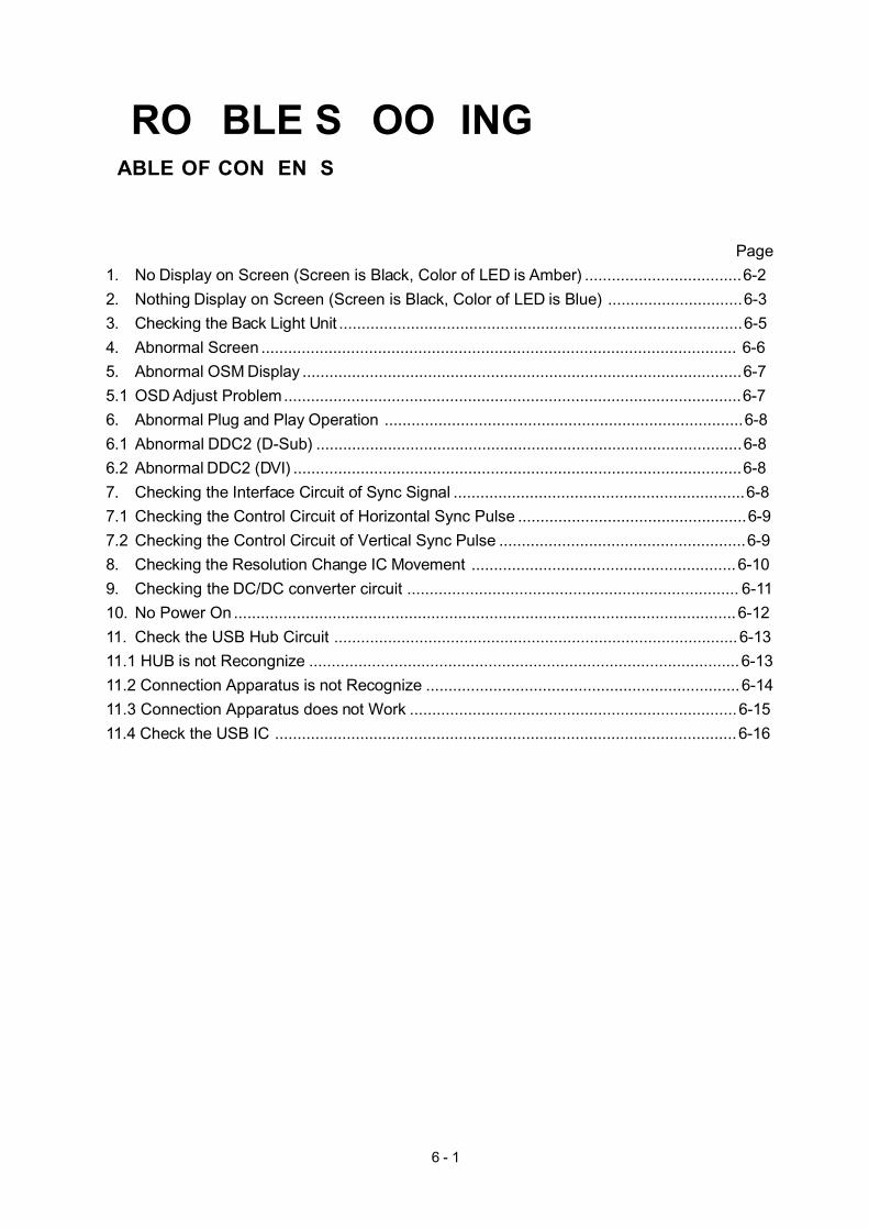
6 - 1
TROUBLE SHOOTINGTABLE OF CONTENTS
Page
1. No Display on Screen (Screen is Black, Color of LED is Amber) ...................................6-2
2. Nothing Display on Screen (Screen is Black, Color of LED is Blue) ..............................6-3
3. Checking the Back Light Unit ..........................................................................................6-5
4. Abnormal Screen .......................................................................................................... 6-6
5. Abnormal OSM Display ..................................................................................................6-7
5.1 OSD Adjust Problem......................................................................................................6-7
6. Abnormal Plug and Play Operation ................................................................................6-8
6.1 Abnormal DDC2 (D-Sub) ...............................................................................................6-8
6.2 Abnormal DDC2 (DVI) ....................................................................................................6-8
7. Checking the Interface Circuit of Sync Signal .................................................................6-8
7.1 Checking the Control Circuit of Horizontal Sync Pulse ...................................................6-9
7.2 Checking the Control Circuit of Vertical Sync Pulse .......................................................6-9
8. Checking the Resolution Change IC Movement ...........................................................6-10
9. Checking the DC/DC converter circuit .......................................................................... 6-11
10. No Power On ................................................................................................................6-12
11. Check the USB Hub Circuit ..........................................................................................6-13
11.1 HUB is not Recongnize ................................................................................................6-13
11.2 Connection Apparatus is not Recognize ......................................................................6-14
11.3 Connection Apparatus does not Work .........................................................................6-15
11.4 Check the USB IC .......................................................................................................6-16

6 - 2
1. No Display of Screen (Screen is Black, Color of LED is Amber)
OK
NG Proceed "5. Abnormal OSM Display"section.
OK
NG Input the sync signal of computer, or change the cable.
Check if the sync signal from Computer is output and if the video
cable is connected normally.
Does OSM display when you push "MENU" button.
Proceed "4. Abnormal Screen" section.
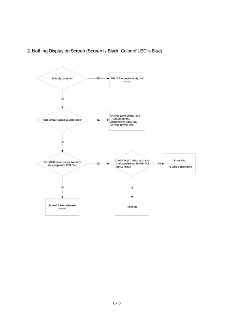
6 - 3
2. Nothing Display on Screen (Screen is Black, Color of LED is Blue)
OK
NG Refer "3. Checking the backlight unit" section
OK
NG1) Change pattern of video signal output on the host.2) Reconnect the video cable.3) Change the video cable.
OK
NG
OK
NGFailure Point
The Cable is disconnected.
Is backlight turned on?
Does computer output RGB video signals?
Check OSM menu is displayed on screen when you push the "MENU" key.
Next PageProceed "4. Abnormal screen" section.
Check if the LCD video signal cable is connected between the MAIN PCB and LCD module.
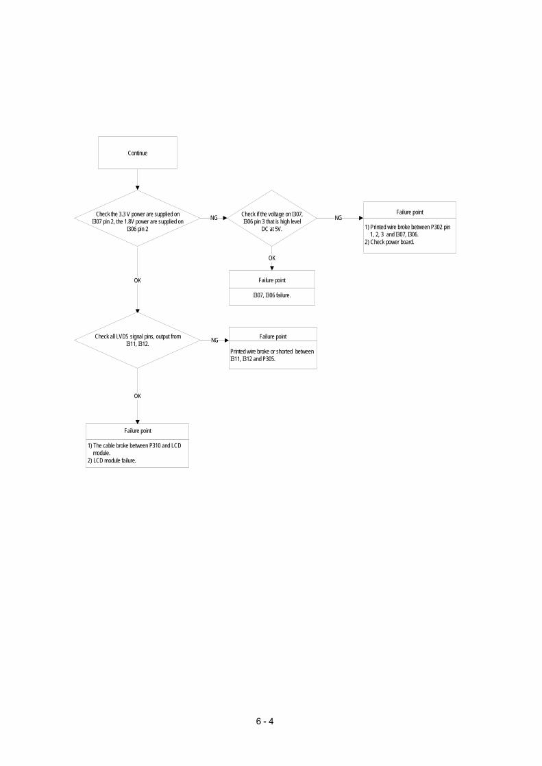
6 - 4
NG
OK
NGFailure point
1) Printed wire broke between P302 pin 1, 2, 3 and I307, I306.2) Check power board.
Failure point
I307, I306 failure.
Failure point
1) The cable broke between P310 and LCD module.2) LCD module failure.
OK
NG Failure point
Printed wire broke or shorted between I311, I312 and P305.
OK
Check the 3.3 V power are supplied on I307 pin 2, the 1.8V power are supplied on
I306 pin 2
Check if the voltage on I307, I306 pin 3 that is high level
DC at 5V.
Check all LVDS signal pins, output from I311, I312.
Continue
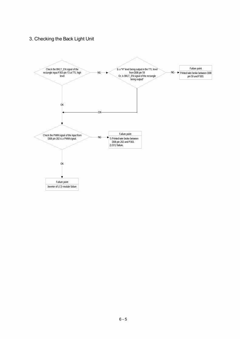
6 - 5
3. Checking the Back Light Unit
OK
NG NGFailure point
Printed wire broke between I308pin 59 and P303.
OK
NGFailure point
1) Printed wire broke between I308 pin 202 and P303.2) I312 failure.
Check the BKLT_EN signal of the rectangle input P303 pin 13 at TTL high
level
Check the PWM signal of the input from I308 pin 202 is a PWM signal.
Failure pointInverter of LCD module failure
Is a "H" level being output in the TTL level from I308 pin 59
Or, is BKLT_EN signal of the rectangle being output?
OK
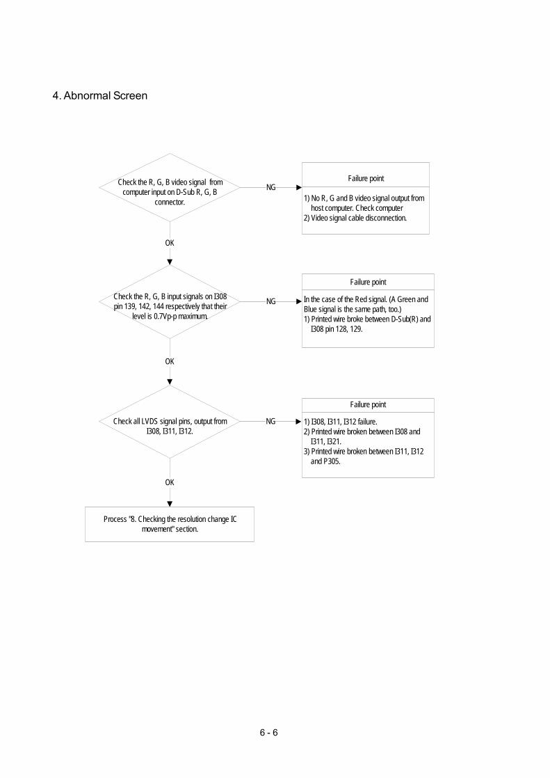
6 - 6
4. Abnormal Screen
OK
NGFailure point
1) No R, G and B video signal output from host computer. Check computer
2) Video signal cable disconnection.
NG
Failure point
In the case of the Red signal. (A Green and Blue signal is the same path, too.)1) Printed wire broke between D-Sub(R) and
I308 pin 128, 129.
OK
OK
NG
Process "8. Checking the resolution change IC movement" section.
Failure point
1) I308, I311, I312 failure.2) Printed wire broken between I308 and I311, I321.3) Printed wire broken between I311, I312 and P305.
Check the R, G, B video signal from computer input on D-Sub R, G, B
connector.
Check the R, G, B input signals on I308 pin 139, 142, 144 respectively that their
level is 0.7Vp-p maximum.
Check all LVDS signal pins, output from I308, I311, I312.
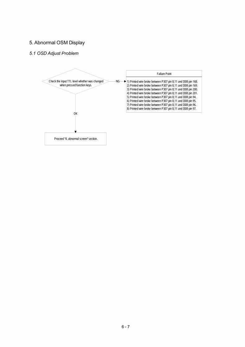
6 - 7
5. Abnormal OSM Display
5.1 OSD Adjust Problem
OK
NG
Proceed "4. abnormal screen" section.
Failure Point
1) Printed wire broke between P307 pin 8,11 and I308 pin 168.2) Printed wire broke between P307 pin 8,11 and I308 pin 169.3) Printed wire broke between P307 pin 8,11 and I308 pin 200.4) Printed wire broke between P307 pin 8,11 and I308 pin 201.5) Printed wire broke between P307 pin 8,11 and I308 pin 94.6) Printed wire broke between P307 pin 8,11 and I308 pin 95.7) Printed wire broke between P307 pin 8,11 and I308 pin 96.8) Printed wire broke between P307 pin 8,11 and I308 pin 97.
Check the input TTL level whether was changed when pressed function keys.

6 - 8
6. Abnormal Plug and Play Operation6.1 Abnormal DDC2 (D-SUB)
6.2 Abnormal DDC2 (DVI)
OK
NGFailure point
I303 failure.
Failure point
1) The host machine isn't communicating in DDC2 mode.2) The video cable may have failed or may not to have
connections for DDC. 3) Between I303 pin 5 and P301 pin 12 may have failed.4) R311, R314 open.5) I303 pin 5 has been shorted.6) Cable failure.7) Same as I303 pin 6.
Confirm the output of serial data on I303 pin 5 synchronize SCLK at TTL level.
OK
NGFailure point
I334 failure.
Failure point
1) The host machine isn't communicating in DDC2 mode.2) The video cable may have failed or may not to have
connections for DDC. 3) Between I334 pin 5 and P304 pin 7 may have failed.4) R318, R506 open.5) I334 pin 5 has been shorted.6) Cable failure.7) Same as I334 pin 6.
Confirm the output of serial data on I334 pin 5 synchronize SCLK at TTL level.
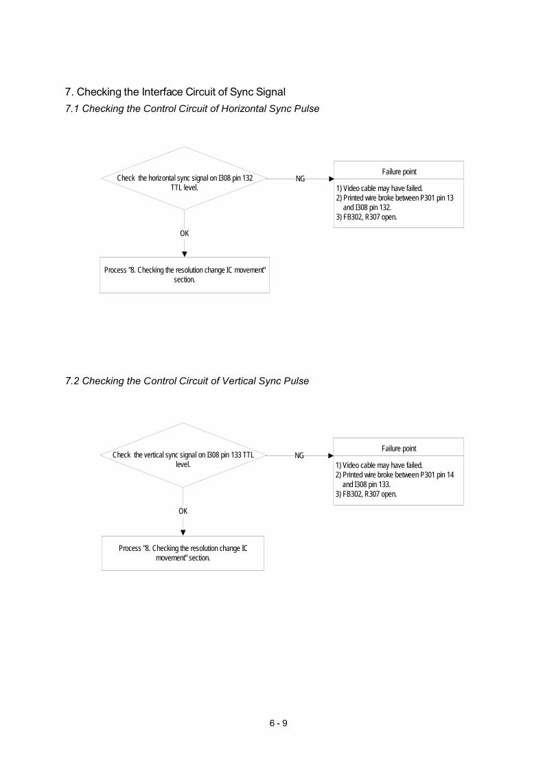
6 - 9
7. Checking the Interface Circuit of Sync Signal
7.1 Checking the Control Circuit of Horizontal Sync Pulse
7.2 Checking the Control Circuit of Vertical Sync Pulse
OK
NGFailure point
1) Video cable may have failed.2) Printed wire broke between P301 pin 13 and I308 pin 132.3) FB302, R307 open.
Process "8. Checking the resolution change IC movement" section.
Check the horizontal sync signal on I308 pin 132 TTL level.
OK
NGFailure point
1) Video cable may have failed.2) Printed wire broke between P301 pin 14 and I308 pin 133.3) FB302, R307 open.
Process "8. Checking the resolution change IC movement" section.
Check the vertical sync signal on I308 pin 133 TTL level.

6 - 10
8. Checking the Resolution Change IC Movement
OK
NG Proceed "9. Checking the DC/DC converter circuit" section.
OK
NG
OK
NG
Failure point
Print wire broke between X301 pin 1 and I308 pin 162.
OK
NG
OK
NG
Failure point
I312 failureFailure point
Print wire broke between SW301 and I308 pin 165.
Failure point
SW301 failure
NG
OK
Proceed "9. Checking the DC/DC converter circuit" section.
Failure point
X301 failure
Is there +3.3V supply on I307 3V3 power pins
Is there +3.3V supply on I306 1V8 power pins
Is 14.318MHz clock input to I308 pin 162 and pin 163 at TTL level during Power On?
Is 14.318MHz clock output from X301 pin 1 at TTL level during Power On?
Is +5.0V supplied to I308 pin 165 at low level (Reset signal)?
Check the output of 0V "L" pulse from SW301.

6 - 11
9. Checking the DC/DC Converter Circuit
OK
NG Printed wire broke between P303 pin 3, 4, 5 and I307, I306 pin 3.
OK
NGFailure point
I307, I306 failure
Failure point
Printed wire broke between I307, I306 pin 2 and I308 power supply pin.
Check if the 5V is output from P303 pin 3, 4, 5 to I307, I306 pin 3.
Check the output of 3.3V, 1.8V line voltage from I307, I306 pin 2.

6 - 12
10. Power Board - No Power ON
OK
NG It is not power board problem.
OK
NG Connect it right.
OK
NG Check F801, D802, P801 and repair them
OK
NG Check D813, L810, I808, C853, ZD802 and repair them.
OK
NG Check peripheral component of I801 and repair them.
OK
NG Check Q802, R840 and repair them.
OK
NG
Check feedback circuit around I807 and the other component and repair them.
OK
NG Repair them.
Check peak voltage of R840 triangle pulse is up to 0.85 volt or not.
Check output voltage +5V is right or not
Check power cord (P801), signal cable, P802, P803 are connected
right or not.
Check C801 is about DC140V-330V or not.
Check C853 is over 16V or not.
Check pin 8 of I808 have same pulse or not.
Check pin 1 of T806 have same pulse or not.
Check peak voltage of R840 triangle pulse is up to 1.5 volt or not.
Check T806, D817, C845, C857 have same short circuit, or the output +5V is over load

6 - 13
11. Check the USB Hub Circuit11.1 HUB is not Recongnize
OK
Failure point
USB cable disconnectionNG
OK
NGFailure point
USB cable disconnection
OK
NG
Failure point
I306 NG
OK
NGFailure point
R434, R433, C499, D331.
OK
OK
Printed wire breaks between X302 and
I308
NG
Proceed "12.4 Check the USB IC " section
Is a cable with the host PC connected
Is a USB cable connected with the monitor?
Is a 3.3V supplied to I319 Vcc Pin 3, 7, 11, 15, 19, 23, 27, 33, 39, 45, 55 ?
Doesn't I306 open
Is a Reset Signal Input toI319 pin 46?
Doesn't clock input to I319 pin 21.
Failure point
X302
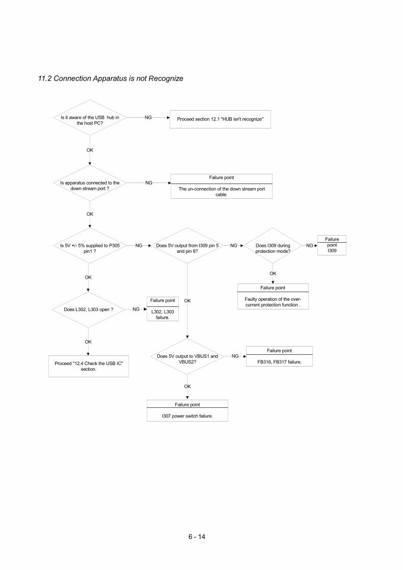
6 - 14
11.2 Connection Apparatus is not Recognize
OK
Proceed section 12.1 "HUB isn't recognize"NG
NG
OK
Failure point
The un-connection of the down stream port cable.
OK
NG
OK
NG
Failure point
FB316, FB317 failure.
Failure point
I307 power switch failure.
OK
NG
Failure point
L302, L303 failure.
OK
NG
Failure point
Faulty operation of the over-current protection function .
Proceed "12.4 Check the USB IC" section.
NGFailure point I309
Is it aware of the USB hub in the host PC?
Is apparatus connected to the down stream port ?
Is 5V +/- 5% supplied to P305 pin1 ?
Does 5V output from I309 pin 5 and pin 8?
Does I309 during protection mode?
OK
Does L302, L303 open ?
Does 5V output to VBUS1 and VBUS2?
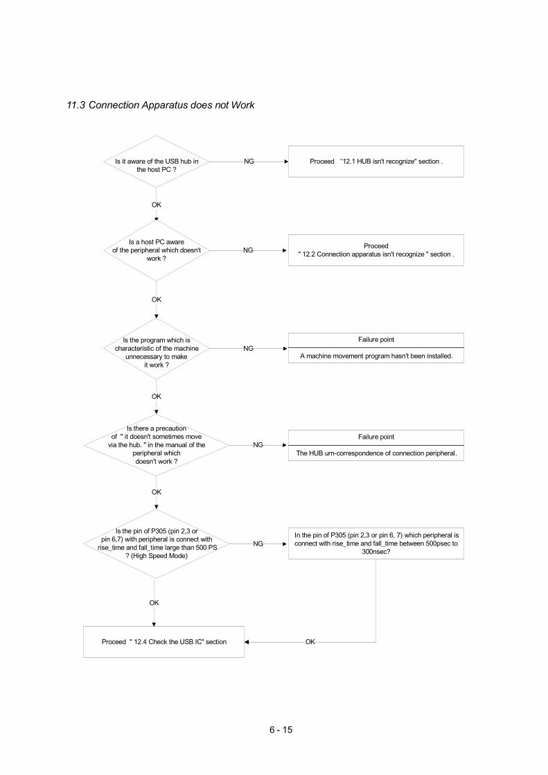
6 - 15
11.3 Connection Apparatus does not Work
OK
NG Proceed “12.1 HUB isn't recognize" section .
Proceed " 12.2 Connection apparatus isn't recognize " section .
OK
NG
OK
NGFailure point
A machine movement program hasn't been installed.
OK
NGFailure point
The HUB urn-correspondence of connection peripheral.
OK
In the pin of P305 (pin 2,3 or pin 6, 7) which peripheral is connect with rise_time and fall_time between 500psec to
300nsec?
Proceed " 12.4 Check the USB IC" section
NG
OK
Is it aware of the USB hub in the host PC ?
Is a host PC aware of the peripheral which doesn't
work ?
Is the program which is characteristic of the machine
unnecessary to make it work ?
Is there a precaution of " it doesn't sometimes move
via the hub. " in the manual of the peripheral which doesn't work ?
Is the pin of P305 (pin 2,3 or pin 6,7) with peripheral is connect with
rise_time and fall_time large than 500 PS ? (High Speed Mode)

6 - 16
11.4 Check the USB IC
NGProceed "9. Check the DC/DC
converter circuit" section.
OK
OK
NG
OK
NG
Failure point
I308 failure
Failure point
X302 failure
NGFailure point
I318, I320 failure
OK
NG
Failure point
Faulty operation of the over current protection function.
Failure point
I318, I320 failure
Is 3.3V supplied to I319 Vcc pin 3,7,11,15,19,23,27,33,39,45,55?
Does X302 oscillate(24 MHz) ?
Does the output of X302 satisfy a threshold level ( High:more than
2.2V,Low:less than 0.8V) ?
Does it have the output of the High Level (more than 4.75V) from I318, I320
Pin 5 and 8?
Does I318, I320 short ?
OK

7- 1
CIRCUIT DESCRIPTIONTABLE OF CONTENTS
Page
1. Interface Board and Panel Power Supply ...................................................................... 7-2
2. Video Input Circuit ........................................................................................................ 7-2
3. System reset, LED Control Circuit ............................................................................... 7-2
4. E2PROM for EDID ........................................................................................................ 7-2
5. E2PROM....................................................................................................................... 7-2
6. MCU Circuit ................................................................................................................... 7-3
7. Power Supply (Circuit daigrams MAIN PWB) ................................................................ 7-6
8. USB 2.0 Hub Circuit ...................................................................................................... 7-8

7- 2
1. Interface Board and Panel Power Supply1.1 P303 connector
A 5V power supply for LCD module, scaler, and logic is generated from the P303 connector.A12V power supply for LCD module.
1.2 I307 , I306, I317 terminal regulatorI307 : A 3.3V power supply for Scaler IC I308 and SDRAM IC I311/I312 are generated from the 5V.I306 : A 1.8V power supply for Video IC I901 and AScaler IC I308 are generated from the 3.3V.I317 : A 3.3V power supply for USB IC I319 is generated from the 5V.I313 ON/OFF control for LCD ModuleI327 ON/OFF control for USB hub circuit.
2. Video Input CircuitThe analog video signal input enters from P306 and P311, the AC-coupled video signal is used to clampthe black level at 0V.The digital TMDS input enters from P302.
3. System Reset, LED Control Circuit3.1 System Reset
System reset is performed by detecting the rising and falling of the 5V source voltage at I308.3.2 LED Control Circuit
Blue / amber control signal of the LED BLUE and LED AMBER signal pin 204, 203 from I308.
4. E2PROM for EDIDThe EDID of Analog input is stored in I303 and the EDID of Digital input is stored in I304 for DVI CE and
I334 for DVI PC to access the information of monitor.
5. E2PROMData transfer between I310 (24LC32B) and scaler IC I308 is effected through the IIC bus SCL (pin 98) andSDA (pin 99) of I308. The data to be transferred to each device are stored in I310. I309 control data. OSD related setting data. Other control data for service menu.●
●
●
7- 3
6. MCU CircuitThe source voltage for I325 is 5V, and the system clock frequency is 11.0529MHz.
6.1 Detection of POWER StatusPower key and RC IR can on/off the system.
6.2 Display Mode Identification6.2.1Functions
(1) Display mode identification The display mode of input signal is identified based on Table 1. When the mode has been identified through the measurement of horizontal and vertical frequencies,
the total number of lines is determined with a formula where Horizontal frequency / Vertical frequency= Total number of lines. Initial identification can be made by examining the coincidence of the obtainedfigure with the number of lines for the mode identified from the frequency.
When the detected frequency if the sync signal has changed, the total number of lines should becounted even through it is rge identified frequency in the same mode.
(2) Power saving mode.This power saving mode is assumed when the frequency of the horizontal and vertical signal is asspecified below.
●
●
●
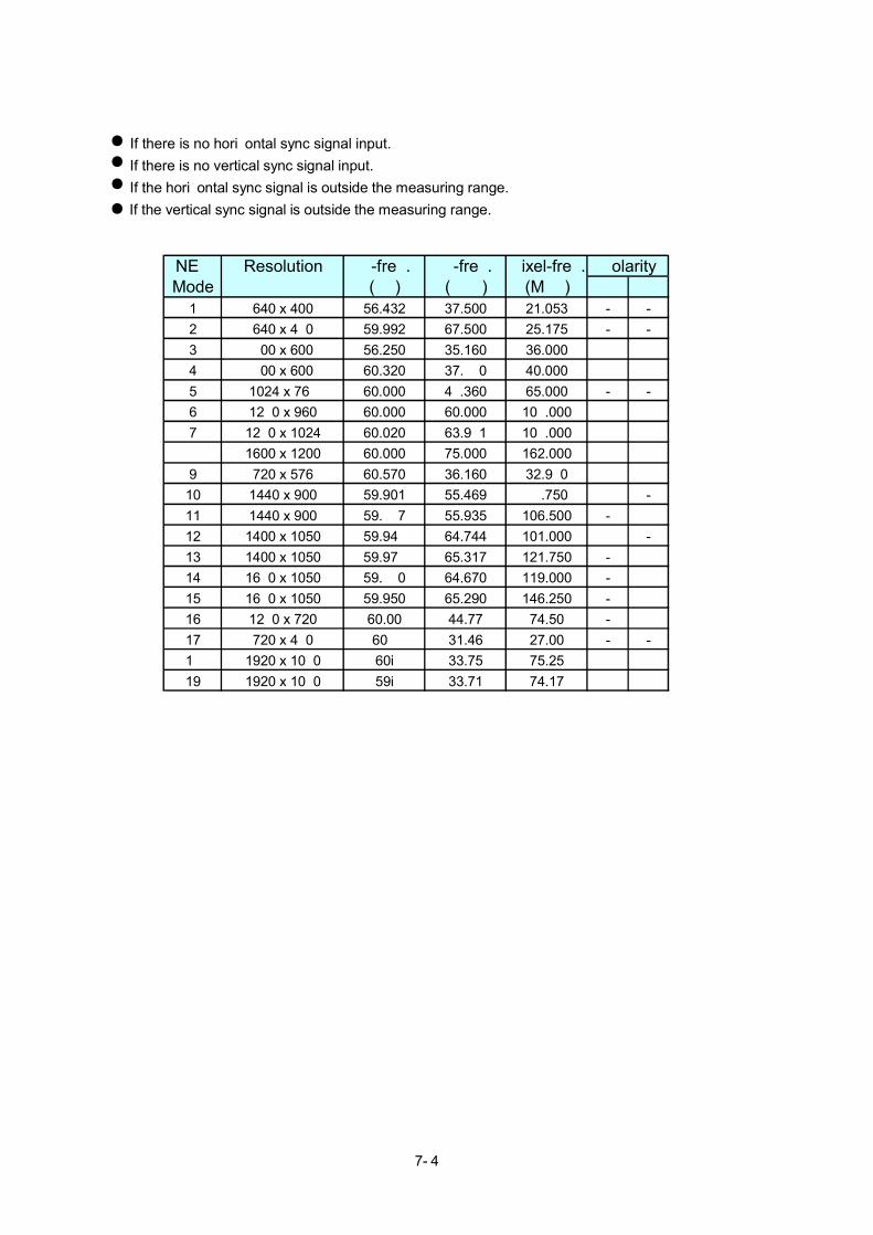
7- 4
If there is no horizontal sync signal input. If there is no vertical sync signal input. If the horizontal sync signal is outside the measuring range. If the vertical sync signal is outside the measuring range.●
●
●
●
NEC Resolution V-freq. H-freq. Pixel-freq.Mode (Hz) (KHz) (MHz) H V
1 640 x 400 56.432 37.500 21.053 - -2 640 x 480 59.992 67.500 25.175 - -3 800 x 600 56.250 35.160 36.000 + +4 800 x 600 60.320 37.880 40.000 + +5 1024 x 768 60.000 48.360 65.000 - -6 1280 x 960 60.000 60.000 108.000 + +7 1280 x 1024 60.020 63.981 108.000 + +8 1600 x 1200 60.000 75.000 162.000 + +9 720 x 576 60.570 36.160 32.980 + +10 1440 x 900 59.901 55.469 88.750 + -11 1440 x 900 59.887 55.935 106.500 - +12 1400 x 1050 59.948 64.744 101.000 + -13 1400 x 1050 59.978 65.317 121.750 - +14 1680 x 1050 59.880 64.670 119.000 - +15 1680 x 1050 59.950 65.290 146.250 - +16 1280 x 720 60.00 44.77 74.50 - +17 720 x 480 60P 31.46 27.00 - -18 1920 x 1080 60i 33.75 75.25 + +19 1920 x 1080 59i 33.71 74.17 + +
Polarity
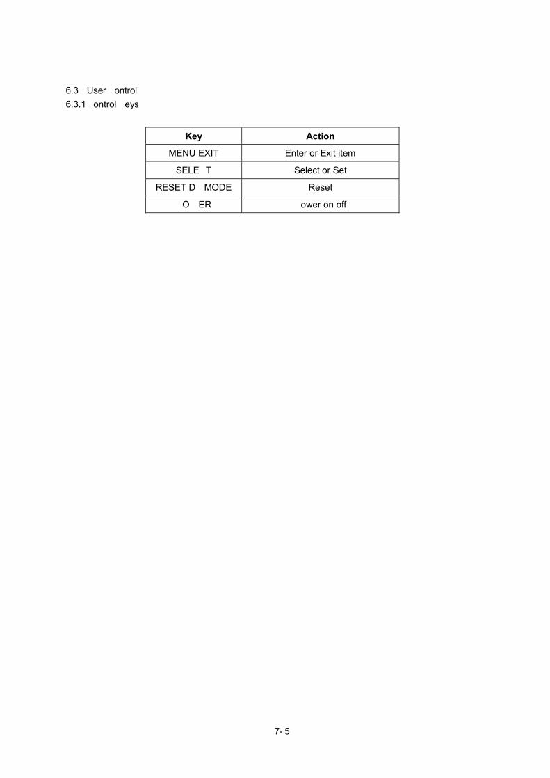
7- 5
6.3 User Control6.3.1Control Keys
Key Action
MENU/EXIT Enter or Exit item
SELECT Select or Set
RESET/DV MODE Reset
POWER Power on/off

7- 6
7. Power Supply (Circuit daigrams MAIN PWB)
7.1 Line filter consists of C802, T802, C808, C805, C836, T803. It eliminates high frequency interference tomeet EMI’s requirement.
7.2 Rec & Filter :Bridge diode D802 converts AC source into pulsed DC. This pulsed DC is smoothed and filtered byC801.R801 is NTC ( negative thermal coefficient ) resistors, used to reduce inrush current to be within safe
range.
7.3 Power transformer :T801 converts energy for square wave from power source C801 to secondary side to generate +24V.T806 cibverts energy for square wave from power source C801 to secondary side to generate +5Vand +12V.
7.4 Output :The square wave from T806 is rectified by D817 and D815, then filtered by C845, C857 and C848,C842 generate +5V, +12V respectively.The square wave from T801 is rectified by D805, then filtered by C811, C814 generate +24Vrespectively.
7.5 Driver :Q802 drive T806 from PWM control of I808 for power converted respectively.Q801 drive T801 from PWM control of I801 for power converted respectively.
7.6 FB :Negative feedback CKT consist of photo coupler I807 and adjustable regulator I806. It can maintainoutput voltages +5V at a stable level.
7.7 PWM :7.7.1 Start (5V): When power is turned on, Q802 conducts due to bias from C801 and R868. I808 starts to
oscillate and outputs a pulse train through pin 8 to drive Q802.7.7.2 OPP (5V): When Q802 turns on, C801 supplies a linearly increasing triangle current through the
primary inductance of T806 to the driver Q802, once the peak value of this current multiplied byR840 exceeds 0.85 volt, pulse train will be shut down immediately to protect Q802, T806 from beingburned out.
7.7.3 Regulation (5V): If output voltage +5V goes up, the R terminal of I808 gets more bias, accordinglyphoto transistor and photo diode flows more current. The voltage of pin 2 goes down, making thepulse width of pin 8 to become narrower. So the output voltage +5V will be pulled down to a stablevalue.
7.7.4 SCP (5V): If output terminal is short to ground, photo transistor does not conduct, then oscillation ofI808 is stop, shuntting Q802 off immediately.
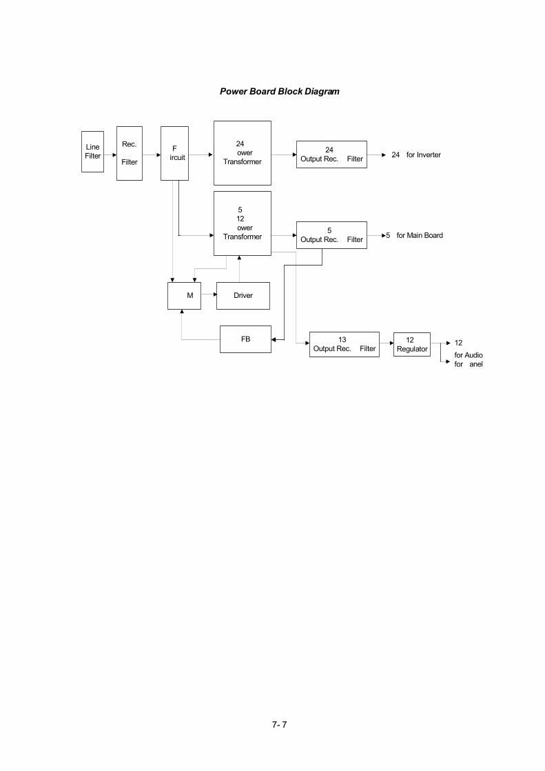
7- 7
Power Board Block Diagram
Line Filter
Rec. &
Filter
5V12V
Power Transformer
5VOutput Rec. & Filter
PWM Driver
FB 13VOutput Rec. & Filter
12V
5V for Main Board
24VPower
Transformer24V
Output Rec. & Filter 24V for Inverter
12VRegulator
for Audiofor Panel
PFC Circuit
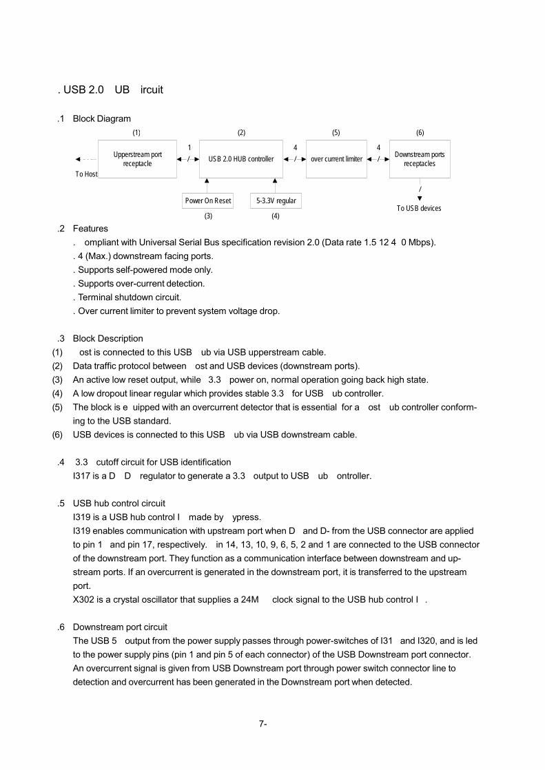
7- 8
8. USB 2.0 HUB Circuit
8.1 Block Diagram
8.2 Features. Compliant with Universal Serial Bus specification revision 2.0 (Data rate 1.5/12/480 Mbps).. 4 (Max.) downstream facing ports.. Supports self-powered mode only.. Supports over-current detection.. Terminal shutdown circuit.. Over current limiter to prevent system voltage drop.
8.3 Block Description(1) Host is connected to this USB Hub via USB upperstream cable.(2) Data traffic protocol between Host and USB devices (downstream ports).(3) An active low reset output, while +3.3V power on, normal operation going back high state.(4) A low dropout linear regular which provides stable 3.3V for USB Hub controller.(5) The block is equipped with an overcurrent detector that is essential for a Host/Hub controller conform-
ing to the USB standard.(6) USB devices is connected to this USB Hub via USB downstream cable.
8.4 3.3V cutoff circuit for USB identificationI317 is a DC/DC regulator to generate a 3.3V output to USB Hub Controller.
8.5 USB hub control circuitI319 is a USB hub control IC made by Cypress.I319 enables communication with upstream port when D+ and D- from the USB connector are appliedto pin 18 and pin 17, respectively. Pin 14, 13, 10, 9, 6, 5, 2 and 1 are connected to the USB connectorof the downstream port. They function as a communication interface between downstream and up-stream ports. If an overcurrent is generated in the downstream port, it is transferred to the upstreamport.X302 is a crystal oscillator that supplies a 24MHz clock signal to the USB hub control IC.
8.6 Downstream port circuitThe USB 5V output from the power supply passes through power-switches of I318 and I320, and is ledto the power supply pins (pin 1 and pin 5 of each connector) of the USB Downstream port connector.An overcurrent signal is given from USB Downstream port through power switch connector line todetection and overcurrent has been generated in the Downstream port when detected.
Upperstream portreceptacle / USB 2.0 HUB controller
Power On Reset 5-3.3V regular
/ over current limiter / Downstream portsreceptacles
To Host
(1) (2)
4
(6)
(3)
(5)
(4)
/
To USB devices
41

8- 1
REPLACEMENT PARTS LISTTABLE OF CONTENTS
PageModel 20WGX2 (B) (For Europe) ........................................................................................................... 8-2
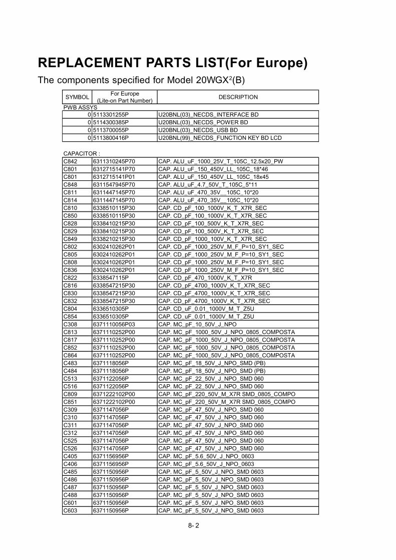
8- 2
REPLACEMENT PARTS LIST(For Europe)The components specified for Model 20WGX2(B)
SYMBOLFor Europe
(Lite-on Part Number)DESCRIPTION
PWB ASSYS0 5113301255P U20BNL(03)_NECDS_INTERFACE BD0 5114300385P U20BNL(03)_NECDS_POWER BD0 5113700055P U20BNL(03)_NECDS_USB BD0 5113800416P U20BNL(99)_NECDS_FUNCTION KEY BD LCD
CAPACITOR :C842 6311310245P70 CAP. ALU_uF_1000_25V_T_105C_12.5x20_PWC801 6312715141P70 CAP. ALU_uF_150_450V_LL_105C_18*46C801 6312715141P01 CAP. ALU_uF_150_450V_LL_105C_18x45C848 6311547945P70 CAP. ALU_uF_4.7_50V_T_105C_5*11C811 6311447145P70 CAP. ALU_uF_470_35V__105C_10*20C814 6311447145P70 CAP. ALU_uF_470_35V__105C_10*20C810 6338510115P30 CAP. CD_pF_100_1000V_K_T_X7R_SECC850 6338510115P30 CAP. CD_pF_100_1000V_K_T_X7R_SECC828 6338410215P30 CAP. CD_pF_100_500V_K_T_X7R_SECC829 6338410215P30 CAP. CD_pF_100_500V_K_T_X7R_SECC849 6338210215P30 CAP. CD_pF_1000_100V_K_T_X7R_SECC802 6302410262P01 CAP. CD_pF_1000_250V_M_F_P=10_SY1_SECC805 6302410262P01 CAP. CD_pF_1000_250V_M_F_P=10_SY1_SECC808 6302410262P01 CAP. CD_pF_1000_250V_M_F_P=10_SY1_SECC836 6302410262P01 CAP. CD_pF_1000_250V_M_F_P=10_SY1_SECC822 6338547115P CAP. CD_pF_470_1000V_K_T_X7RC816 6338547215P30 CAP. CD_pF_4700_1000V_K_T_X7R_SECC830 6338547215P30 CAP. CD_pF_4700_1000V_K_T_X7R_SECC832 6338547215P30 CAP. CD_pF_4700_1000V_K_T_X7R_SECC804 6336510305P CAP. CD_uF_0.01_1000V_M_T_Z5UC854 6336510305P CAP. CD_uF_0.01_1000V_M_T_Z5UC308 6371110056P03 CAP. MC_pF_10_50V_J_NPOC813 6371110252P00 CAP. MC_pF_1000_50V_J_NPO_0805_COMPOSTAC817 6371110252P00 CAP. MC_pF_1000_50V_J_NPO_0805_COMPOSTAC852 6371110252P00 CAP. MC_pF_1000_50V_J_NPO_0805_COMPOSTAC864 6371110252P00 CAP. MC_pF_1000_50V_J_NPO_0805_COMPOSTAC483 6371118056P CAP. MC_pF_18_50V_J_NPO_SMD (PB)C484 6371118056P CAP. MC_pF_18_50V_J_NPO_SMD (PB)C513 6371122056P CAP. MC_pF_22_50V_J_NPO_SMD 060C516 6371122056P CAP. MC_pF_22_50V_J_NPO_SMD 060C809 6371222102P00 CAP. MC_pF_220_50V_M_X7R SMD_0805_COMPOC851 6371222102P00 CAP. MC_pF_220_50V_M_X7R SMD_0805_COMPOC309 6371147056P CAP. MC_pF_47_50V_J_NPO_SMD 060C310 6371147056P CAP. MC_pF_47_50V_J_NPO_SMD 060C311 6371147056P CAP. MC_pF_47_50V_J_NPO_SMD 060C312 6371147056P CAP. MC_pF_47_50V_J_NPO_SMD 060C525 6371147056P CAP. MC_pF_47_50V_J_NPO_SMD 060C526 6371147056P CAP. MC_pF_47_50V_J_NPO_SMD 060C405 6371156956P CAP. MC_pF_5.6_50V_J_NPO_0603C406 6371156956P CAP. MC_pF_5.6_50V_J_NPO_0603C485 6371150956P CAP. MC_pF_5_50V_J_NPO_SMD 0603C486 6371150956P CAP. MC_pF_5_50V_J_NPO_SMD 0603C487 6371150956P CAP. MC_pF_5_50V_J_NPO_SMD 0603C488 6371150956P CAP. MC_pF_5_50V_J_NPO_SMD 0603C601 6371150956P CAP. MC_pF_5_50V_J_NPO_SMD 0603C603 6371150956P CAP. MC_pF_5_50V_J_NPO_SMD 0603
8- 3
SYMBOL For Europe(Lite-on Part Number) DESCRIPTION
C604 6371150956P CAP. MC_pF_5_50V_J_NPO_SMD 0603C605 6371150956P CAP. MC_pF_5_50V_J_NPO_SMD 0603C517 6371156156P03 CAP. MC_pF_560_50V_J_NPOC304 6371210356P CAP. MC_uF_0.01_50V_J_X7R_C330 6371210356P CAP. MC_uF_0.01_50V_J_X7R_C407 6371210356P CAP. MC_uF_0.01_50V_J_X7R_C408 6371210356P CAP. MC_uF_0.01_50V_J_X7R_C409 6371210356P CAP. MC_uF_0.01_50V_J_X7R_C410 6371210356P CAP. MC_uF_0.01_50V_J_X7R_C819 6371210312P CAP. MC_uF_0.01_50V_K_X7R_SMD 0805C847 6371210312P CAP. MC_uF_0.01_50V_K_X7R_SMD 0805C862 6373210412P CAP. MC_uF_0.1_25V_K_X7R_SMD 0805C302 6371210416P CAP. MC_uF_0.1_50V_K_X7R_SMD 0603 PBC303 6371210416P CAP. MC_uF_0.1_50V_K_X7R_SMD 0603 PBC305 6371210416P CAP. MC_uF_0.1_50V_K_X7R_SMD 0603 PBC307 6371210416P CAP. MC_uF_0.1_50V_K_X7R_SMD 0603 PBC314 6371210416P CAP. MC_uF_0.1_50V_K_X7R_SMD 0603 PBC316 6371210416P CAP. MC_uF_0.1_50V_K_X7R_SMD 0603 PBC317 6371210416P CAP. MC_uF_0.1_50V_K_X7R_SMD 0603 PBC320 6371210416P CAP. MC_uF_0.1_50V_K_X7R_SMD 0603 PBC321 6371210416P CAP. MC_uF_0.1_50V_K_X7R_SMD 0603 PBC322 6371210416P CAP. MC_uF_0.1_50V_K_X7R_SMD 0603 PBC324 6371210416P CAP. MC_uF_0.1_50V_K_X7R_SMD 0603 PBC325 6371210416P CAP. MC_uF_0.1_50V_K_X7R_SMD 0603 PBC327 6371210416P CAP. MC_uF_0.1_50V_K_X7R_SMD 0603 PBC328 6371210416P CAP. MC_uF_0.1_50V_K_X7R_SMD 0603 PBC329 6371210416P CAP. MC_uF_0.1_50V_K_X7R_SMD 0603 PBC331 6371210416P CAP. MC_uF_0.1_50V_K_X7R_SMD 0603 PBC333 6371210416P CAP. MC_uF_0.1_50V_K_X7R_SMD 0603 PBC334 6371210416P CAP. MC_uF_0.1_50V_K_X7R_SMD 0603 PBC335 6371210416P CAP. MC_uF_0.1_50V_K_X7R_SMD 0603 PBC336 6371210416P CAP. MC_uF_0.1_50V_K_X7R_SMD 0603 PBC337 6371210416P CAP. MC_uF_0.1_50V_K_X7R_SMD 0603 PBC338 6371210416P CAP. MC_uF_0.1_50V_K_X7R_SMD 0603 PBC339 6371210416P CAP. MC_uF_0.1_50V_K_X7R_SMD 0603 PBC340 6371210416P CAP. MC_uF_0.1_50V_K_X7R_SMD 0603 PBC341 6371210416P CAP. MC_uF_0.1_50V_K_X7R_SMD 0603 PBC342 6371210416P CAP. MC_uF_0.1_50V_K_X7R_SMD 0603 PBC344 6371210416P CAP. MC_uF_0.1_50V_K_X7R_SMD 0603 PBC346 6371210416P CAP. MC_uF_0.1_50V_K_X7R_SMD 0603 PBC353 6371210416P CAP. MC_uF_0.1_50V_K_X7R_SMD 0603 PBC355 6371210416P CAP. MC_uF_0.1_50V_K_X7R_SMD 0603 PBC359 6371210416P CAP. MC_uF_0.1_50V_K_X7R_SMD 0603 PBC361 6371210416P CAP. MC_uF_0.1_50V_K_X7R_SMD 0603 PBC366 6371210416P CAP. MC_uF_0.1_50V_K_X7R_SMD 0603 PBC367 6371210416P CAP. MC_uF_0.1_50V_K_X7R_SMD 0603 PBC368 6371210416P CAP. MC_uF_0.1_50V_K_X7R_SMD 0603 PBC369 6371210416P CAP. MC_uF_0.1_50V_K_X7R_SMD 0603 PBC370 6371210416P CAP. MC_uF_0.1_50V_K_X7R_SMD 0603 PBC371 6371210416P CAP. MC_uF_0.1_50V_K_X7R_SMD 0603 PBC372 6371210416P CAP. MC_uF_0.1_50V_K_X7R_SMD 0603 PBC373 6371210416P CAP. MC_uF_0.1_50V_K_X7R_SMD 0603 PBC374 6371210416P CAP. MC_uF_0.1_50V_K_X7R_SMD 0603 PBC375 6371210416P CAP. MC_uF_0.1_50V_K_X7R_SMD 0603 PB

8- 4
SYMBOL For Europe(Lite-on Part Number) DESCRIPTION
C376 6371210416P CAP. MC_uF_0.1_50V_K_X7R_SMD 0603 PBC377 6371210416P CAP. MC_uF_0.1_50V_K_X7R_SMD 0603 PBC378 6371210416P CAP. MC_uF_0.1_50V_K_X7R_SMD 0603 PBC379 6371210416P CAP. MC_uF_0.1_50V_K_X7R_SMD 0603 PBC380 6371210416P CAP. MC_uF_0.1_50V_K_X7R_SMD 0603 PBC384 6371210416P CAP. MC_uF_0.1_50V_K_X7R_SMD 0603 PBC385 6371210416P CAP. MC_uF_0.1_50V_K_X7R_SMD 0603 PBC386 6371210416P CAP. MC_uF_0.1_50V_K_X7R_SMD 0603 PBC387 6371210416P CAP. MC_uF_0.1_50V_K_X7R_SMD 0603 PBC388 6371210416P CAP. MC_uF_0.1_50V_K_X7R_SMD 0603 PBC389 6371210416P CAP. MC_uF_0.1_50V_K_X7R_SMD 0603 PBC390 6371210416P CAP. MC_uF_0.1_50V_K_X7R_SMD 0603 PBC391 6371210416P CAP. MC_uF_0.1_50V_K_X7R_SMD 0603 PBC392 6371210416P CAP. MC_uF_0.1_50V_K_X7R_SMD 0603 PBC396 6371210416P CAP. MC_uF_0.1_50V_K_X7R_SMD 0603 PBC397 6371210416P CAP. MC_uF_0.1_50V_K_X7R_SMD 0603 PBC398 6371210416P CAP. MC_uF_0.1_50V_K_X7R_SMD 0603 PBC399 6371210416P CAP. MC_uF_0.1_50V_K_X7R_SMD 0603 PBC400 6371210416P CAP. MC_uF_0.1_50V_K_X7R_SMD 0603 PBC401 6371210416P CAP. MC_uF_0.1_50V_K_X7R_SMD 0603 PBC404 6371210416P CAP. MC_uF_0.1_50V_K_X7R_SMD 0603 PBC411 6371210416P CAP. MC_uF_0.1_50V_K_X7R_SMD 0603 PBC412 6371210416P CAP. MC_uF_0.1_50V_K_X7R_SMD 0603 PBC414 6371210416P CAP. MC_uF_0.1_50V_K_X7R_SMD 0603 PBC417 6371210416P CAP. MC_uF_0.1_50V_K_X7R_SMD 0603 PBC419 6371210416P CAP. MC_uF_0.1_50V_K_X7R_SMD 0603 PBC420 6371210416P CAP. MC_uF_0.1_50V_K_X7R_SMD 0603 PBC421 6371210416P CAP. MC_uF_0.1_50V_K_X7R_SMD 0603 PBC422 6371210416P CAP. MC_uF_0.1_50V_K_X7R_SMD 0603 PBC427 6371210416P CAP. MC_uF_0.1_50V_K_X7R_SMD 0603 PBC428 6371210416P CAP. MC_uF_0.1_50V_K_X7R_SMD 0603 PBC429 6371210416P CAP. MC_uF_0.1_50V_K_X7R_SMD 0603 PBC430 6371210416P CAP. MC_uF_0.1_50V_K_X7R_SMD 0603 PBC431 6371210416P CAP. MC_uF_0.1_50V_K_X7R_SMD 0603 PBC432 6371210416P CAP. MC_uF_0.1_50V_K_X7R_SMD 0603 PBC433 6371210416P CAP. MC_uF_0.1_50V_K_X7R_SMD 0603 PBC434 6371210416P CAP. MC_uF_0.1_50V_K_X7R_SMD 0603 PBC446 6371210416P CAP. MC_uF_0.1_50V_K_X7R_SMD 0603 PBC447 6371210416P CAP. MC_uF_0.1_50V_K_X7R_SMD 0603 PBC448 6371210416P CAP. MC_uF_0.1_50V_K_X7R_SMD 0603 PBC456 6371210416P CAP. MC_uF_0.1_50V_K_X7R_SMD 0603 PBC457 6371210416P CAP. MC_uF_0.1_50V_K_X7R_SMD 0603 PBC459 6371210416P CAP. MC_uF_0.1_50V_K_X7R_SMD 0603 PBC462 6371210416P CAP. MC_uF_0.1_50V_K_X7R_SMD 0603 PBC464 6371210416P CAP. MC_uF_0.1_50V_K_X7R_SMD 0603 PBC465 6371210416P CAP. MC_uF_0.1_50V_K_X7R_SMD 0603 PBC468 6371210416P CAP. MC_uF_0.1_50V_K_X7R_SMD 0603 PBC469 6371210416P CAP. MC_uF_0.1_50V_K_X7R_SMD 0603 PBC470 6371210416P CAP. MC_uF_0.1_50V_K_X7R_SMD 0603 PBC471 6371210416P CAP. MC_uF_0.1_50V_K_X7R_SMD 0603 PBC472 6371210416P CAP. MC_uF_0.1_50V_K_X7R_SMD 0603 PBC473 6371210416P CAP. MC_uF_0.1_50V_K_X7R_SMD 0603 PBC474 6371210416P CAP. MC_uF_0.1_50V_K_X7R_SMD 0603 PBC475 6371210416P CAP. MC_uF_0.1_50V_K_X7R_SMD 0603 PB
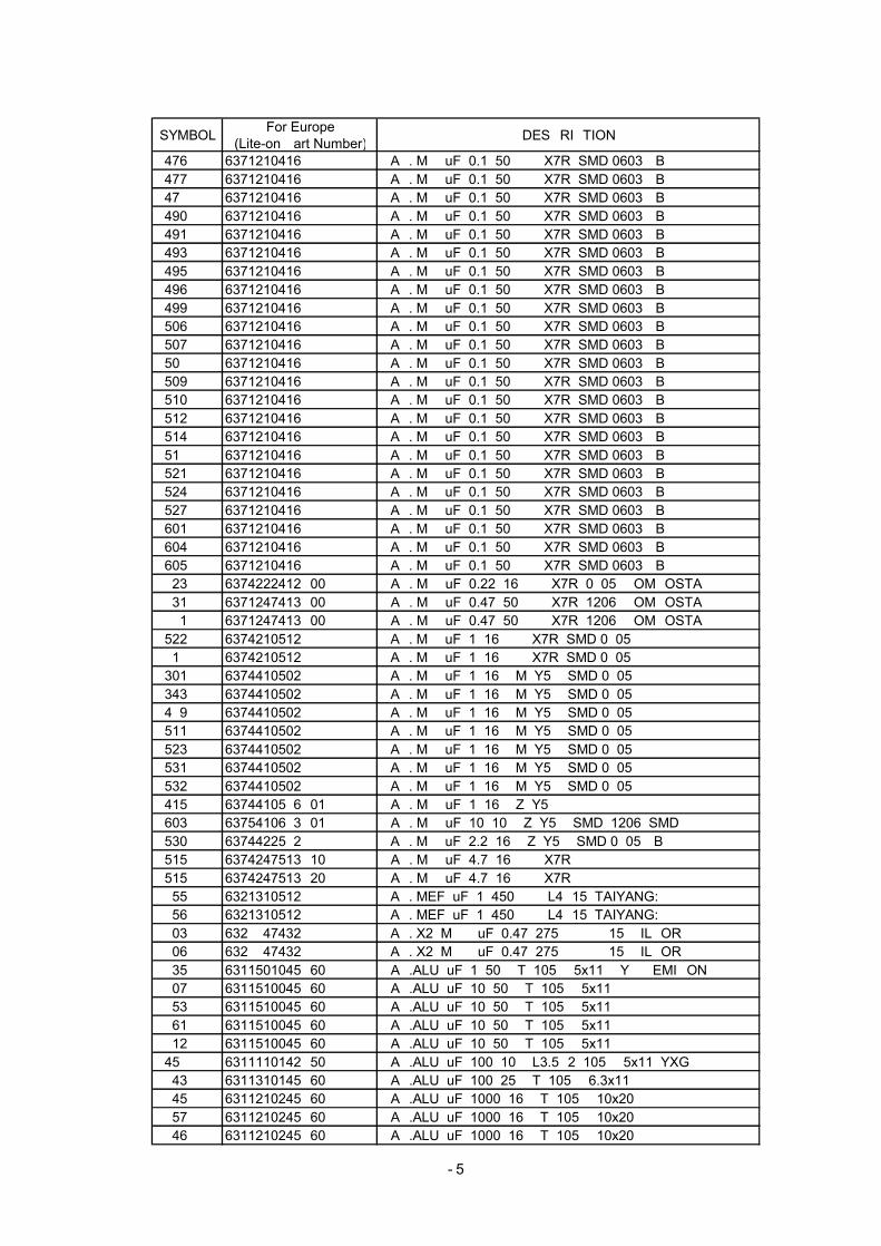
8- 5
SYMBOL For Europe(Lite-on Part Number) DESCRIPTION
C476 6371210416P CAP. MC_uF_0.1_50V_K_X7R_SMD 0603 PBC477 6371210416P CAP. MC_uF_0.1_50V_K_X7R_SMD 0603 PBC478 6371210416P CAP. MC_uF_0.1_50V_K_X7R_SMD 0603 PBC490 6371210416P CAP. MC_uF_0.1_50V_K_X7R_SMD 0603 PBC491 6371210416P CAP. MC_uF_0.1_50V_K_X7R_SMD 0603 PBC493 6371210416P CAP. MC_uF_0.1_50V_K_X7R_SMD 0603 PBC495 6371210416P CAP. MC_uF_0.1_50V_K_X7R_SMD 0603 PBC496 6371210416P CAP. MC_uF_0.1_50V_K_X7R_SMD 0603 PBC499 6371210416P CAP. MC_uF_0.1_50V_K_X7R_SMD 0603 PBC506 6371210416P CAP. MC_uF_0.1_50V_K_X7R_SMD 0603 PBC507 6371210416P CAP. MC_uF_0.1_50V_K_X7R_SMD 0603 PBC508 6371210416P CAP. MC_uF_0.1_50V_K_X7R_SMD 0603 PBC509 6371210416P CAP. MC_uF_0.1_50V_K_X7R_SMD 0603 PBC510 6371210416P CAP. MC_uF_0.1_50V_K_X7R_SMD 0603 PBC512 6371210416P CAP. MC_uF_0.1_50V_K_X7R_SMD 0603 PBC514 6371210416P CAP. MC_uF_0.1_50V_K_X7R_SMD 0603 PBC518 6371210416P CAP. MC_uF_0.1_50V_K_X7R_SMD 0603 PBC521 6371210416P CAP. MC_uF_0.1_50V_K_X7R_SMD 0603 PBC524 6371210416P CAP. MC_uF_0.1_50V_K_X7R_SMD 0603 PBC527 6371210416P CAP. MC_uF_0.1_50V_K_X7R_SMD 0603 PBC601 6371210416P CAP. MC_uF_0.1_50V_K_X7R_SMD 0603 PBC604 6371210416P CAP. MC_uF_0.1_50V_K_X7R_SMD 0603 PBC605 6371210416P CAP. MC_uF_0.1_50V_K_X7R_SMD 0603 PBC823 6374222412P00 CAP. MC_uF_0.22_16V_K_X7R_0805_COMPOSTAC831 6371247413P00 CAP. MC_uF_0.47_50V_K_X7R_1206_COMPOSTAC881 6371247413P00 CAP. MC_uF_0.47_50V_K_X7R_1206_COMPOSTAC522 6374210512P CAP. MC_uF_1_16V_K_X7R_SMD 0805C818 6374210512P CAP. MC_uF_1_16V_K_X7R_SMD 0805C301 6374410502P CAP. MC_uF_1_16V_M_Y5V_SMD 0805C343 6374410502P CAP. MC_uF_1_16V_M_Y5V_SMD 0805C489 6374410502P CAP. MC_uF_1_16V_M_Y5V_SMD 0805C511 6374410502P CAP. MC_uF_1_16V_M_Y5V_SMD 0805C523 6374410502P CAP. MC_uF_1_16V_M_Y5V_SMD 0805C531 6374410502P CAP. MC_uF_1_16V_M_Y5V_SMD 0805C532 6374410502P CAP. MC_uF_1_16V_M_Y5V_SMD 0805C415 6374410586P01 CAP. MC_uF_1_16V_Z_Y5V_C603 6375410683P01 CAP. MC_uF_10_10V_Z_Y5V_SMD_1206_SMDC530 6374422582P CAP. MC_uF_2.2_16V_Z_Y5V_SMD 0805 PBC515 6374247513P10 CAP. MC_uF_4.7_16V_K_X7R_C515 6374247513P20 CAP. MC_uF_4.7_16V_K_X7R_C855 6321310512P CAP. MEF_uF_1_450V_K_L4P15_TAIYANG:C856 6321310512P CAP. MEF_uF_1_450V_K_L4P15_TAIYANG:C803 6328847432P CAP. X2_MPP_uF_0.47_275V_K_P=15_PILKORC806 6328847432P CAP. X2_MPP_uF_0.47_275V_K_P=15_PILKORC835 6311501045P60 CAP.ALU_uF_1_50V_T_105C_5x11_KY/CHEMICONC807 6311510045P60 CAP.ALU_uF_10_50V_T_105C_5x11_C853 6311510045P60 CAP.ALU_uF_10_50V_T_105C_5x11_C861 6311510045P60 CAP.ALU_uF_10_50V_T_105C_5x11_C812 6311510045P60 CAP.ALU_uF_10_50V_T_105C_5x11_C458 6311110142P50 CAP.ALU_uF_100_10V_L3.5P2_105C_5x11_YXG/C843 6311310145P60 CAP.ALU_uF_100_25V_T_105C_6.3x11_C845 6311210245P60 CAP.ALU_uF_1000_16V_T_105C_10x20_C857 6311210245P60 CAP.ALU_uF_1000_16V_T_105C_10x20_C846 6311210245P60 CAP.ALU_uF_1000_16V_T_105C_10x20_

8- 6
SYMBOL For Europe(Lite-on Part Number) DESCRIPTION
C846 6311210245P72 CAP.ALU_uF_1000_16V_T_105C_10x20_PW/NICHC356 6311122142P60 CAP.ALU_uF_220_10V_L3.5P2.5_105C_6.3x11_C360 6311122142P60 CAP.ALU_uF_220_10V_L3.5P2.5_105C_6.3x11_C362 6311122142P60 CAP.ALU_uF_220_10V_L3.5P2.5_105C_6.3x11_C454 6311122142P60 CAP.ALU_uF_220_10V_L3.5P2.5_105C_6.3x11_C461 6311122142P60 CAP.ALU_uF_220_10V_L3.5P2.5_105C_6.3x11_C463 6311122142P60 CAP.ALU_uF_220_10V_L3.5P2.5_105C_6.3x11_C492 6311122142P60 CAP.ALU_uF_220_10V_L3.5P2.5_105C_6.3x11_C494 6311122142P60 CAP.ALU_uF_220_10V_L3.5P2.5_105C_6.3x11_C347 6311322142P60 CAP.ALU_uF_220_25V_L3.5P3.5_105C_8x11.5_C416 6311322142P60 CAP.ALU_uF_220_25V_L3.5P3.5_105C_8x11.5_C820 6311547945P60 CAP.ALU_uF_4.7_50V_T_105C_5x11_C365 6311347042P60 CAP.ALU_uF_47_25V_L3.5P2_105C_5x11_KY/NCC382 6311347042P60 CAP.ALU_uF_47_25V_L3.5P2_105C_5x11_KY/NCC383 6311347042P60 CAP.ALU_uF_47_25V_L3.5P2_105C_5x11_KY/NCC394 6311347042P60 CAP.ALU_uF_47_25V_L3.5P2_105C_5x11_KY/NCC395 6311347042P60 CAP.ALU_uF_47_25V_L3.5P2_105C_5x11_KY/NCC403 6311347042P60 CAP.ALU_uF_47_25V_L3.5P2_105C_5x11_KY/NCC418 6311347042P60 CAP.ALU_uF_47_25V_L3.5P2_105C_5x11_KY/NCC426 6311347042P60 CAP.ALU_uF_47_25V_L3.5P2_105C_5x11_KY/NCCOIL AND FILTER :L301 6111000028P COIL CHOKE_COMMON(SMD)_OHM_160_25%L302 6111000028P COIL CHOKE_COMMON(SMD)_OHM_160_25%L303 6111000028P COIL CHOKE_COMMON(SMD)_OHM_160_25%L304 6111000028P COIL CHOKE_COMMON(SMD)_OHM_160_25%L305 6111000028P COIL CHOKE_COMMON(SMD)_OHM_160_25%L801 6111285131P COIL CHOKE_PFC_uH_282.5_+_13%_T80_52_LSEL803 6111549130P COIL CHOKE_uH_5.4_KL810 6115479104P00 COIL PEAKING_uH_4.7_K_T26_STAR/AL0307TBT802 6138000002P00 LINE FILTER_mH_12_ET24_LSE(FLI5005EL)T803 6138003601P LINE FILTER_mH_14_FR16*12*8_LSE(TUBE)FB301 6881101898P CORE_BEAD_BK 2125 HS 431_TIAYOFB302 6881101898P CORE_BEAD_BK 2125 HS 431_TIAYOFB332 6881102378P CORE_BEAD_PBY201209T_170Y_S_CHILISINFB334 6881102378P CORE_BEAD_PBY201209T_170Y_S_CHILISINFB343 6881102378P CORE_BEAD_PBY201209T_170Y_S_CHILISINFB344 6881102378P CORE_BEAD_PBY201209T_170Y_S_CHILISINFB345 6881102378P CORE_BEAD_PBY201209T_170Y_S_CHILISINFB346 6881102378P CORE_BEAD_PBY201209T_170Y_S_CHILISINFB347 6881102378P CORE_BEAD_PBY201209T_170Y_S_CHILISINFB348 6881102378P CORE_BEAD_PBY201209T_170Y_S_CHILISINFB303 6881102178P CORE_BEAD_PBY201209T_300Y_S_CHILISINFB304 6881102178P CORE_BEAD_PBY201209T_300Y_S_CHILISINFB305 6881102178P CORE_BEAD_PBY201209T_300Y_S_CHILISINFB312 6881102178P CORE_BEAD_PBY201209T_300Y_S_CHILISINFB313 6881102178P CORE_BEAD_PBY201209T_300Y_S_CHILISINFB314 6881102178P CORE_BEAD_PBY201209T_300Y_S_CHILISINFB315 6881102178P CORE_BEAD_PBY201209T_300Y_S_CHILISINFB316 6881102178P CORE_BEAD_PBY201209T_300Y_S_CHILISINFB317 6881102178P CORE_BEAD_PBY201209T_300Y_S_CHILISINFB321 6881102178P CORE_BEAD_PBY201209T_300Y_S_CHILISINFB322 6881102178P CORE_BEAD_PBY201209T_300Y_S_CHILISINFB324 6881102178P CORE_BEAD_PBY201209T_300Y_S_CHILISINFB325 6881102178P CORE_BEAD_PBY201209T_300Y_S_CHILISIN
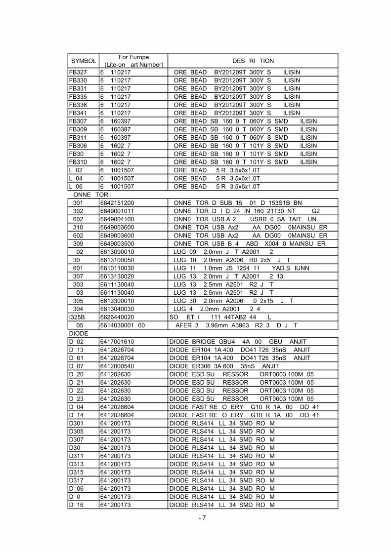
8- 7
SYMBOL For Europe(Lite-on Part Number) DESCRIPTION
FB327 6881102178P CORE_BEAD_PBY201209T_300Y_S_CHILISINFB330 6881102178P CORE_BEAD_PBY201209T_300Y_S_CHILISINFB331 6881102178P CORE_BEAD_PBY201209T_300Y_S_CHILISINFB335 6881102178P CORE_BEAD_PBY201209T_300Y_S_CHILISINFB336 6881102178P CORE_BEAD_PBY201209T_300Y_S_CHILISINFB341 6881102178P CORE_BEAD_PBY201209T_300Y_S_CHILISINFB307 6881603978P CORE_BEAD_SBK160808T_060Y_S_SMD_CHILISINFB309 6881603978P CORE_BEAD_SBK160808T_060Y_S_SMD_CHILISINFB311 6881603978P CORE_BEAD_SBK160808T_060Y_S_SMD_CHILISINFB306 6881602878P CORE_BEAD_SBK160808T_101Y_S_SMD_CHILISINFB308 6881602878P CORE_BEAD_SBK160808T_101Y_S_SMD_CHILISINFB310 6881602878P CORE_BEAD_SBK160808T_101Y_S_SMD_CHILISINL802 6881001507P CORE_BEAD_W5 RH3.5x6x1.0TL804 6881001507P CORE_BEAD_W5 RH3.5x6x1.0TL806 6881001507P CORE_BEAD_W5 RH3.5x6x1.0TCONNECTOR :P301 6642151200P CONNECTOR_D_SUB_15P_01CD_153S1B_BNP302 6649001011P CONNECTOR_DVI_D_24PIN_160821130_NTK_CHG2P602 6649004100P CONNECTOR_USB A*2_8P_USBR_08SA_TAITWUNP310 6649003600P CONNECTOR_USB_Ax2_8P_AACDG008K0MAINSUPERP602 6649003600P CONNECTOR_USB_Ax2_8P_AACDG008K0MAINSUPERP309 6649003500P CONNECTOR_USB_B_4P_ABDWX004K0_MAINSUPERP802 6613090010P PLUG_09P_2.0mm_JWT_A2001WV2P308 6613100050P PLUG_10P_2.0mm_A2006WR0_2x5P_JWTP601 6610110030P PLUG_11P_1.0mm_JS_1254_11_CHYAD SHIUNNP307 6613130020P PLUG_13P_2.0mm_JWT_A2001WV2_13P303 6611130040P PLUG_13P_2.5mm_A2501WR2_JWTP803 6611130040P PLUG_13P_2.5mm_A2501WR2_JWTP305 6613300010P PLUG_30P_2.0mm_A2006WV0_2x15P_JWTP304 6613040030P PLUG_4P_2.0mm_A2001WV2_4I325B 6626440020P SOCKET_IC_8111_44TAB2_44P_PLCCP805 6614030001P00 WAFER_3P_3.96mm_A3963WR2_3P_D_JWTDIODED802 6417001610P DIODE_BRIDGE_GBU4K_4A/800V_GBU_PANJITD813 6412026704P DIODE_ER104_1A/400V_DO41/T26_35nS_PANJITD861 6412026704P DIODE_ER104_1A/400V_DO41/T26_35nS_PANJITD807 6412000540P DIODE_ER306_3A/600V_35nS_PANJITD820 6412026308P DIODE_ESD SUPPRESSOR_VPORT0603 100MV05D821 6412026308P DIODE_ESD SUPPRESSOR_VPORT0603 100MV05D822 6412026308P DIODE_ESD SUPPRESSOR_VPORT0603 100MV05D823 6412026308P DIODE_ESD SUPPRESSOR_VPORT0603 100MV05D804 6412026604P DIODE_FAST RECOVERY_PG108R_1A/800V_DO_41D814 6412026604P DIODE_FAST RECOVERY_PG108R_1A/800V_DO_41D301 6412001738P DIODE_RLS4148 LL_34_SMD_ROHMD305 6412001738P DIODE_RLS4148 LL_34_SMD_ROHMD307 6412001738P DIODE_RLS4148 LL_34_SMD_ROHMD308 6412001738P DIODE_RLS4148 LL_34_SMD_ROHMD311 6412001738P DIODE_RLS4148 LL_34_SMD_ROHMD313 6412001738P DIODE_RLS4148 LL_34_SMD_ROHMD315 6412001738P DIODE_RLS4148 LL_34_SMD_ROHMD317 6412001738P DIODE_RLS4148 LL_34_SMD_ROHMD806 6412001738P DIODE_RLS4148 LL_34_SMD_ROHMD808 6412001738P DIODE_RLS4148 LL_34_SMD_ROHMD816 6412001738P DIODE_RLS4148 LL_34_SMD_ROHM
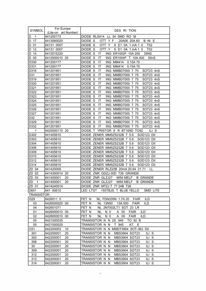
8- 8
SYMBOL For Europe(Lite-on Part Number) DESCRIPTION
D881 6412001738P DIODE_RLS4148 LL_34_SMD_ROHMD817 6413060020P DIODE_SCHOTTKY_FCQ20A06_20A/60V_B_NICED801 6413180007P DIODE_SCHOTTKY_P6KE180A_1 mA/180V_T52D812 6413180007P DIODE_SCHOTTKY_P6KE180A_1 mA/180V_T52D815 6412015220P DIODE_SWITCHING_ER1002F_10A/200V_35NSD805 6412000010P20 DIODE_SWITCHING_ER1004FCT_10A/400V_50nS_D330 6412001778P DIODE_SWITCHING_MM4148_0.15A/75D331 6412001778P DIODE_SWITCHING_MM4148_0.15A/75D316 6412019518P DIODE_SWITCHING_MMBD7000_7_75V_SOT23_4nSD318 6412019518P DIODE_SWITCHING_MMBD7000_7_75V_SOT23_4nSD319 6412019518P DIODE_SWITCHING_MMBD7000_7_75V_SOT23_4nSD320 6412019518P DIODE_SWITCHING_MMBD7000_7_75V_SOT23_4nSD321 6412019518P DIODE_SWITCHING_MMBD7000_7_75V_SOT23_4nSD322 6412019518P DIODE_SWITCHING_MMBD7000_7_75V_SOT23_4nSD323 6412019518P DIODE_SWITCHING_MMBD7000_7_75V_SOT23_4nSD324 6412019518P DIODE_SWITCHING_MMBD7000_7_75V_SOT23_4nSD325 6412019518P DIODE_SWITCHING_MMBD7000_7_75V_SOT23_4nSD326 6412019518P DIODE_SWITCHING_MMBD7000_7_75V_SOT23_4nSD327 6412019518P DIODE_SWITCHING_MMBD7000_7_75V_SOT23_4nSD328 6412019518P DIODE_SWITCHING_MMBD7000_7_75V_SOT23_4nSD329 6412019518P DIODE_SWITCHING_MMBD7000_7_75V_SOT23_4nSD332 6412019518P DIODE_SWITCHING_MMBD7000_7_75V_SOT23_4nSQ881 6425000115P20 DIODE_THYRISTOR_SCR_BT169D_TO92_PHILIPSD302 6414056108P DIODE_ZENER_MMSZ5232B_7_5.6V_SOD123_DIID303 6414056108P DIODE_ZENER_MMSZ5232B_7_5.6V_SOD123_DIID304 6414056108P DIODE_ZENER_MMSZ5232B_7_5.6V_SOD123_DIID306 6414056108P DIODE_ZENER_MMSZ5232B_7_5.6V_SOD123_DIID309 6414056108P DIODE_ZENER_MMSZ5232B_7_5.6V_SOD123_DIID310 6414056108P DIODE_ZENER_MMSZ5232B_7_5.6V_SOD123_DIID312 6414056108P DIODE_ZENER_MMSZ5232B_7_5.6V_SOD123_DIID314 6414056108P DIODE_ZENER_MMSZ5232B_7_5.6V_SOD123_DIIZD804 6414200098P DIODE_ZENER_RLZ22B_20mA/20.64~21.71V_LLZD802 6414300014P20 DIODE_ZNR_GDZJ-30D_T26_GRANDEZD803 6414000018P20 DIODE_ZNR_GLZJ27C_MINI MELF_PB_GRANDEZD881 6414000018P20 DIODE_ZNR_GLZJ27C_MINI MELF_PB_GRANDEZD801 6414240014P DIODE_ZNR_MTZJ T_77 24B_T26D601 6418006108P LED_LTST_C155TBJSKT_BLUE/YELLOW_SMD_LITETRANSISTOR :I329 6426011808P FET_N CHNL_FDN335N_1.7A/20V_FAIRCHILDQ803 6426000020P00 FET_N_CHNL_13N50C_13A/500V_FAIRCHILDQ804 6426010718P FET_N_CHNL_2N7002LT1_SOT_23_LRCQ801 6426000010P00 FET_N_CHNL_8N80C_8A/800V_FAIRCHILDQ802 6426000010P00 FET_N_CHNL_8N80C_8A/800V_FAIRCHILDQ805 6421000535P TRANSISTOR_NPN_2SC945P_TO_92_B/Q805 6421000525P TRANSISTOR_NPN_KTC945_P_AT_KECI331 6422000038P10 TRANSISTOR_NPN_MMDT3904_SOT-363_DIIQ301 6422000018P20 TRANSISTOR_NPN_PMBS3904_SOT23_PHILIPSQ302 6422000018P20 TRANSISTOR_NPN_PMBS3904_SOT23_PHILIPSQ306 6422000018P20 TRANSISTOR_NPN_PMBS3904_SOT23_PHILIPSQ308 6422000018P20 TRANSISTOR_NPN_PMBS3904_SOT23_PHILIPSQ309 6422000018P20 TRANSISTOR_NPN_PMBS3904_SOT23_PHILIPSQ312 6422000018P20 TRANSISTOR_NPN_PMBS3904_SOT23_PHILIPSQ313 6422000018P20 TRANSISTOR_NPN_PMBS3904_SOT23_PHILIPSQ314 6422000018P20 TRANSISTOR_NPN_PMBS3904_SOT23_PHILIPS

8- 9
SYMBOL For Europe(Lite-on Part Number) DESCRIPTION
Q316 6422000018P20 TRANSISTOR_NPN_PMBS3904_SOT23_PHILIPSQ320 6422000018P20 TRANSISTOR_NPN_PMBS3904_SOT23_PHILIPSQ321 6422000018P20 TRANSISTOR_NPN_PMBS3904_SOT23_PHILIPSQ323 6422000018P20 TRANSISTOR_NPN_PMBS3904_SOT23_PHILIPSQ326 6422000018P20 TRANSISTOR_NPN_PMBS3904_SOT23_PHILIPSQ808 6423000225P TRANSISTOR_PNP_2SA733P_T0_92_B/Q808 6423000215P TRANSISTOR_PNP_KTA733_P_AT_TOQ303 6423000018P20 TRANSISTOR_PNP_PMBS3906_SOT23_PHILIPSQ304 6423000018P20 TRANSISTOR_PNP_PMBS3906_SOT23_PHILIPSQ317 6423000018P20 TRANSISTOR_PNP_PMBS3906_SOT23_PHILIPSQ318 6423000018P20 TRANSISTOR_PNP_PMBS3906_SOT23_PHILIPSQ319 6423000018P20 TRANSISTOR_PNP_PMBS3906_SOT23_PHILIPSQ322 6423000018P20 TRANSISTOR_PNP_PMBS3906_SOT23_PHILIPSQ324 6423000018P20 TRANSISTOR_PNP_PMBS3906_SOT23_PHILIPSQ327 6423000018P20 TRANSISTOR_PNP_PMBS3906_SOT23_PHILIPSQ328 6423000018P20 TRANSISTOR_PNP_PMBS3906_SOT23_PHILIPSIC :I318 6442034308P IC_AIC1526_0PS_8PIN_SOP_AICI320 6442034308P IC_AIC1526_0PS_8PIN_SOP_AICI313 6444014708P IC_CMOS_AO3401_3P_SOT23_AOS(ALPHA&OMEGA)I308 6444000086P21 IC_CMOS_GM5861_208P_PQFP_GENESISI311 6448000158P40 IC_CMOS_M12L16161A-5TG_50P_TSOP_ESMTI312 6448000158P40 IC_CMOS_M12L16161A-5TG_50P_TSOP_ESMTI309 6448027108P IC_CMOS_SST25LF040A_33_4C_S2AE_8P_SOIC_SI303 6448018208P IC_CPU_24LC02BT/SN_8PIN_SOIC_MICROCHIPI334 6448018208P IC_CPU_24LC02BT/SN_8PIN_SOIC_MICROCHIPI310 6448018308P IC_CPU_24LC32AT/SNG_8PIN_SOIC_MICROCHIPI319 6448022018P IC_CPU_CY7C65640A_LFXC 56P QFN_TAPPINGI325 6448018900P50 IC_CPU_SM89516C25J_44P_PLCC_SYNCMOSI332 6442000068P24 IC_LINEAR(OP)_LMV358MX_8P_SOIC_NSI317 6442043008P IC_LINEAR_AIC1117A_33PYTR_3PIN_SOT_223_AI327 6442027348P IC_LINEAR_AO4407_8P_SO8_AOSI328 6442027348P IC_LINEAR_AO4407_8P_SO8_AOSI803 6442041005P IC_LINEAR_AP431VLA_3P_TO 92_ANACHIPI806 6442041005P IC_LINEAR_AP431VLA_3P_TO 92_ANACHIPI306 6442044008P IC_LINEAR_LM1085ISX-ADJ_3P_TO-263_NS_MSLI307 6442044008P IC_LINEAR_LM1085ISX-ADJ_3P_TO-263_NS_MSLI802 6442014000P IC_Linear_LTV_817D_4P_PDIPI807 6442014000P IC_Linear_LTV_817D_4P_PDIPI813 6442014000P IC_Linear_LTV_817D_4P_PDIPI801 6442000048P05 IC_LINEAR_SG6841SZ3_8P_SMD_SGI808 6442000048P05 IC_LINEAR_SG6841SZ3_8P_SMD_SGI809 6444000018P03 IC_PFC_L6562DTR_8P_SO8_STI324 6446008108P IC_TTL_NC7SZ04M5X_5P_FAIRCHILDI326 6446000028P14 IC_TTL_SN74HC14PWR_14P_TSSOP_TII323 6446008708P IC_TTL_SN74LV4052APWR_16P_TSSOP_TEXASI333 6446008708P IC_TTL_SN74LV4052APWR_16P_TSSOP_TEXASI804 6442030200P IC-LINEAR-KA78R12C-4P-TO-220F-4L-FAIRCHIRESISTOR :R816 6253120152P RES. CHIP_R_KOHM_1.2_1/8W_J_805R819 6252100142P RES. CHIP_R_KOHM_1_1/10W_F_805R820 6252100142P RES. CHIP_R_KOHM_1_1/10W_F_805R842 6252100142P RES. CHIP_R_KOHM_1_1/10W_F_805R843 6252100142P RES. CHIP_R_KOHM_1_1/10W_F_805
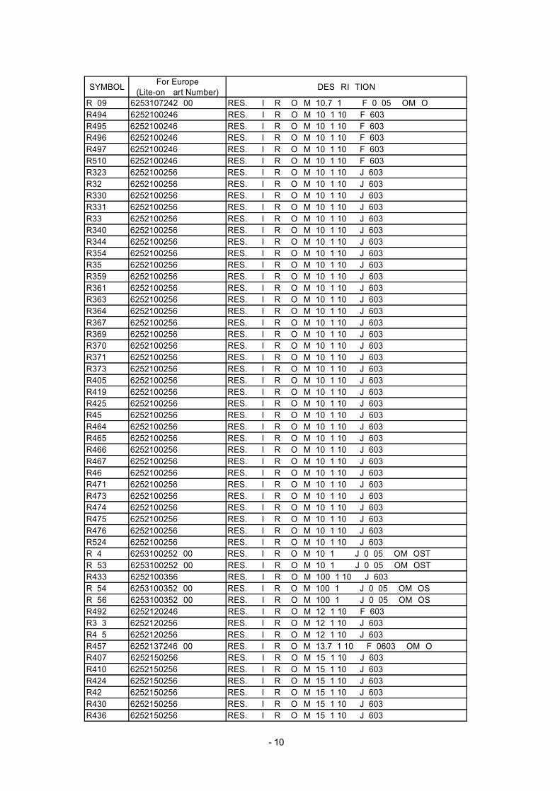
8- 10
SYMBOL For Europe(Lite-on Part Number) DESCRIPTION
R809 6253107242P00 RES. CHIP_R_KOHM_10.7_1/8W_F_0805_COMPOR494 6252100246P RES. CHIP_R_KOHM_10_1/10W_F_603R495 6252100246P RES. CHIP_R_KOHM_10_1/10W_F_603R496 6252100246P RES. CHIP_R_KOHM_10_1/10W_F_603R497 6252100246P RES. CHIP_R_KOHM_10_1/10W_F_603R510 6252100246P RES. CHIP_R_KOHM_10_1/10W_F_603R323 6252100256P RES. CHIP_R_KOHM_10_1/10W_J_603R328 6252100256P RES. CHIP_R_KOHM_10_1/10W_J_603R330 6252100256P RES. CHIP_R_KOHM_10_1/10W_J_603R331 6252100256P RES. CHIP_R_KOHM_10_1/10W_J_603R338 6252100256P RES. CHIP_R_KOHM_10_1/10W_J_603R340 6252100256P RES. CHIP_R_KOHM_10_1/10W_J_603R344 6252100256P RES. CHIP_R_KOHM_10_1/10W_J_603R354 6252100256P RES. CHIP_R_KOHM_10_1/10W_J_603R358 6252100256P RES. CHIP_R_KOHM_10_1/10W_J_603R359 6252100256P RES. CHIP_R_KOHM_10_1/10W_J_603R361 6252100256P RES. CHIP_R_KOHM_10_1/10W_J_603R363 6252100256P RES. CHIP_R_KOHM_10_1/10W_J_603R364 6252100256P RES. CHIP_R_KOHM_10_1/10W_J_603R367 6252100256P RES. CHIP_R_KOHM_10_1/10W_J_603R369 6252100256P RES. CHIP_R_KOHM_10_1/10W_J_603R370 6252100256P RES. CHIP_R_KOHM_10_1/10W_J_603R371 6252100256P RES. CHIP_R_KOHM_10_1/10W_J_603R373 6252100256P RES. CHIP_R_KOHM_10_1/10W_J_603R405 6252100256P RES. CHIP_R_KOHM_10_1/10W_J_603R419 6252100256P RES. CHIP_R_KOHM_10_1/10W_J_603R425 6252100256P RES. CHIP_R_KOHM_10_1/10W_J_603R458 6252100256P RES. CHIP_R_KOHM_10_1/10W_J_603R464 6252100256P RES. CHIP_R_KOHM_10_1/10W_J_603R465 6252100256P RES. CHIP_R_KOHM_10_1/10W_J_603R466 6252100256P RES. CHIP_R_KOHM_10_1/10W_J_603R467 6252100256P RES. CHIP_R_KOHM_10_1/10W_J_603R468 6252100256P RES. CHIP_R_KOHM_10_1/10W_J_603R471 6252100256P RES. CHIP_R_KOHM_10_1/10W_J_603R473 6252100256P RES. CHIP_R_KOHM_10_1/10W_J_603R474 6252100256P RES. CHIP_R_KOHM_10_1/10W_J_603R475 6252100256P RES. CHIP_R_KOHM_10_1/10W_J_603R476 6252100256P RES. CHIP_R_KOHM_10_1/10W_J_603R524 6252100256P RES. CHIP_R_KOHM_10_1/10W_J_603R848 6253100252P00 RES. CHIP_R_KOHM_10_1/8W_J_0805_COMPOSTR853 6253100252P00 RES. CHIP_R_KOHM_10_1/8W_J_0805_COMPOSTR433 6252100356P RES. CHIP_R_KOHM_100_1/10W_J_603R854 6253100352P00 RES. CHIP_R_KOHM_100_1/8W_J_0805_COMPOSR856 6253100352P00 RES. CHIP_R_KOHM_100_1/8W_J_0805_COMPOSR492 6252120246P RES. CHIP_R_KOHM_12_1/10W_F_603R383 6252120256P RES. CHIP_R_KOHM_12_1/10W_J_603R485 6252120256P RES. CHIP_R_KOHM_12_1/10W_J_603R457 6252137246P00 RES. CHIP_R_KOHM_13.7_1/10W_F_0603_COMPOR407 6252150256P RES. CHIP_R_KOHM_15_1/10W_J_603R410 6252150256P RES. CHIP_R_KOHM_15_1/10W_J_603R424 6252150256P RES. CHIP_R_KOHM_15_1/10W_J_603R428 6252150256P RES. CHIP_R_KOHM_15_1/10W_J_603R430 6252150256P RES. CHIP_R_KOHM_15_1/10W_J_603R436 6252150256P RES. CHIP_R_KOHM_15_1/10W_J_603
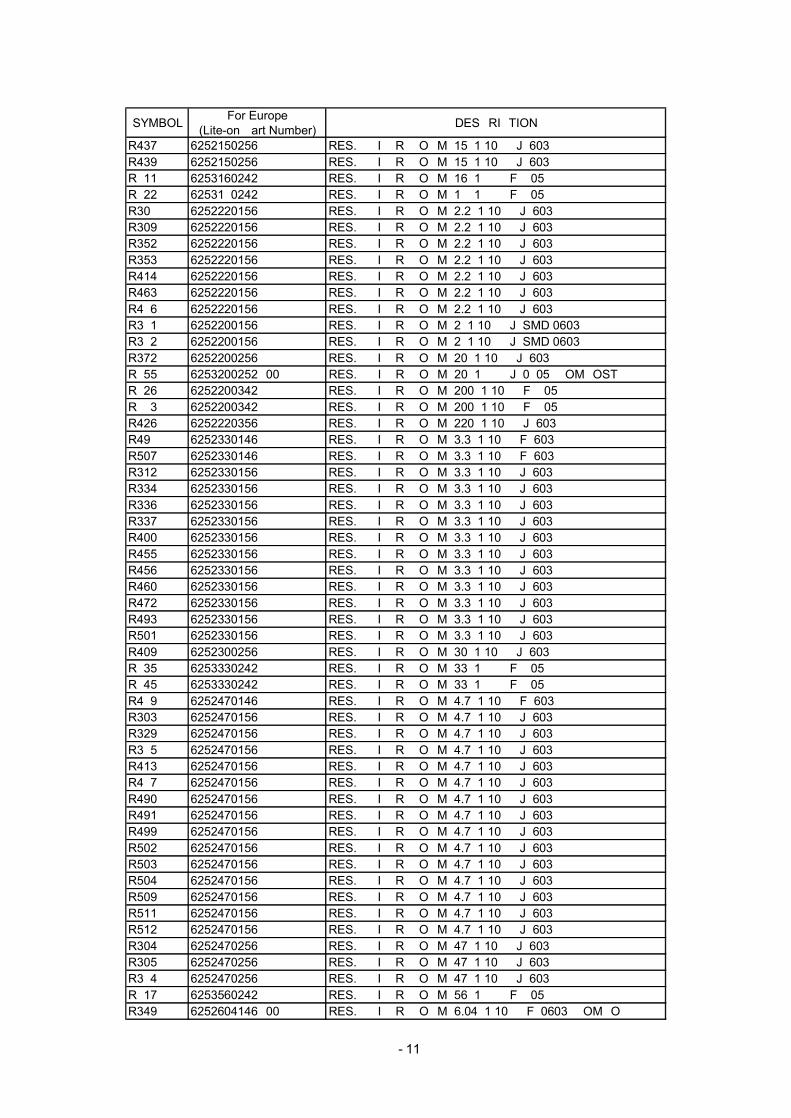
8- 11
SYMBOL For Europe(Lite-on Part Number) DESCRIPTION
R437 6252150256P RES. CHIP_R_KOHM_15_1/10W_J_603R439 6252150256P RES. CHIP_R_KOHM_15_1/10W_J_603R811 6253160242P RES. CHIP_R_KOHM_16_1/8W_F_805R822 6253180242P RES. CHIP_R_KOHM_18_1/8W_F_805R308 6252220156P RES. CHIP_R_KOHM_2.2_1/10W_J_603R309 6252220156P RES. CHIP_R_KOHM_2.2_1/10W_J_603R352 6252220156P RES. CHIP_R_KOHM_2.2_1/10W_J_603R353 6252220156P RES. CHIP_R_KOHM_2.2_1/10W_J_603R414 6252220156P RES. CHIP_R_KOHM_2.2_1/10W_J_603R463 6252220156P RES. CHIP_R_KOHM_2.2_1/10W_J_603R486 6252220156P RES. CHIP_R_KOHM_2.2_1/10W_J_603R381 6252200156P RES. CHIP_R_KOHM_2_1/10W_J_SMD 0603R382 6252200156P RES. CHIP_R_KOHM_2_1/10W_J_SMD 0603R372 6252200256P RES. CHIP_R_KOHM_20_1/10W_J_603R855 6253200252P00 RES. CHIP_R_KOHM_20_1/8W_J_0805_COMPOSTR826 6252200342P RES. CHIP_R_KOHM_200_1/10W_F_805R883 6252200342P RES. CHIP_R_KOHM_200_1/10W_F_805R426 6252220356P RES. CHIP_R_KOHM_220_1/10W_J_603R498 6252330146P RES. CHIP_R_KOHM_3.3_1/10W_F_603R507 6252330146P RES. CHIP_R_KOHM_3.3_1/10W_F_603R312 6252330156P RES. CHIP_R_KOHM_3.3_1/10W_J_603R334 6252330156P RES. CHIP_R_KOHM_3.3_1/10W_J_603R336 6252330156P RES. CHIP_R_KOHM_3.3_1/10W_J_603R337 6252330156P RES. CHIP_R_KOHM_3.3_1/10W_J_603R400 6252330156P RES. CHIP_R_KOHM_3.3_1/10W_J_603R455 6252330156P RES. CHIP_R_KOHM_3.3_1/10W_J_603R456 6252330156P RES. CHIP_R_KOHM_3.3_1/10W_J_603R460 6252330156P RES. CHIP_R_KOHM_3.3_1/10W_J_603R472 6252330156P RES. CHIP_R_KOHM_3.3_1/10W_J_603R493 6252330156P RES. CHIP_R_KOHM_3.3_1/10W_J_603R501 6252330156P RES. CHIP_R_KOHM_3.3_1/10W_J_603R409 6252300256P RES. CHIP_R_KOHM_30_1/10W_J_603R835 6253330242P RES. CHIP_R_KOHM_33_1/8W_F_805R845 6253330242P RES. CHIP_R_KOHM_33_1/8W_F_805R489 6252470146P RES. CHIP_R_KOHM_4.7_1/10W_F_603R303 6252470156P RES. CHIP_R_KOHM_4.7_1/10W_J_603R329 6252470156P RES. CHIP_R_KOHM_4.7_1/10W_J_603R385 6252470156P RES. CHIP_R_KOHM_4.7_1/10W_J_603R413 6252470156P RES. CHIP_R_KOHM_4.7_1/10W_J_603R487 6252470156P RES. CHIP_R_KOHM_4.7_1/10W_J_603R490 6252470156P RES. CHIP_R_KOHM_4.7_1/10W_J_603R491 6252470156P RES. CHIP_R_KOHM_4.7_1/10W_J_603R499 6252470156P RES. CHIP_R_KOHM_4.7_1/10W_J_603R502 6252470156P RES. CHIP_R_KOHM_4.7_1/10W_J_603R503 6252470156P RES. CHIP_R_KOHM_4.7_1/10W_J_603R504 6252470156P RES. CHIP_R_KOHM_4.7_1/10W_J_603R509 6252470156P RES. CHIP_R_KOHM_4.7_1/10W_J_603R511 6252470156P RES. CHIP_R_KOHM_4.7_1/10W_J_603R512 6252470156P RES. CHIP_R_KOHM_4.7_1/10W_J_603R304 6252470256P RES. CHIP_R_KOHM_47_1/10W_J_603R305 6252470256P RES. CHIP_R_KOHM_47_1/10W_J_603R384 6252470256P RES. CHIP_R_KOHM_47_1/10W_J_603R817 6253560242P RES. CHIP_R_KOHM_56_1/8W_F_805R349 6252604146P00 RES. CHIP_R_KOHM_6.04_1/10W_F_0603_COMPO

8- 12
SYMBOL For Europe(Lite-on Part Number) DESCRIPTION
R823 6253649142P00 RES. CHIP_R_KOHM_6.49_1/8W_F_0805_COMPOR825 6252649342P RES. CHIP_R_KOHM_649_1/10W_F_805R396 6252820356P RES. CHIP_R_KOHM_820_0.1W_J_TAPINGR397 6252820356P RES. CHIP_R_KOHM_820_0.1W_J_TAPINGR421 6252100456P RES. CHIP_R_MOHM_1_1/10W_J_603R477 6252100456P RES. CHIP_R_MOHM_1_1/10W_J_603R821 6254100443P00 RES. CHIP_R_MOHM_1_1/4W_F_1206_COMPOSTAR867 6254100443P00 RES. CHIP_R_MOHM_1_1/4W_F_1206_COMPOSTAR350 6252000056P RES. CHIP_R_OHM_0_1/10W_J_603R351 6252000056P RES. CHIP_R_OHM_0_1/10W_J_603R408 6252000056P RES. CHIP_R_OHM_0_1/10W_J_603R411 6252000056P RES. CHIP_R_OHM_0_1/10W_J_603R429 6252000056P RES. CHIP_R_OHM_0_1/10W_J_603R431 6252000056P RES. CHIP_R_OHM_0_1/10W_J_603R469 6252000056P RES. CHIP_R_OHM_0_1/10W_J_603R302 6252100056P RES. CHIP_R_OHM_100_1/10W_J_603R307 6252100056P RES. CHIP_R_OHM_100_1/10W_J_603R313 6252100056P RES. CHIP_R_OHM_100_1/10W_J_603R314 6252100056P RES. CHIP_R_OHM_100_1/10W_J_603R317 6252100056P RES. CHIP_R_OHM_100_1/10W_J_603R318 6252100056P RES. CHIP_R_OHM_100_1/10W_J_603R319 6252100056P RES. CHIP_R_OHM_100_1/10W_J_603R322 6252100056P RES. CHIP_R_OHM_100_1/10W_J_603R332 6252100056P RES. CHIP_R_OHM_100_1/10W_J_603R423 6252100056P RES. CHIP_R_OHM_100_1/10W_J_603R434 6252100056P RES. CHIP_R_OHM_100_1/10W_J_603R610 6252113046P RES. CHIP_R_OHM_113_1/10W_F_0603R611 6252113046P RES. CHIP_R_OHM_113_1/10W_F_0603R481 6252120046P RES. CHIP_R_OHM_120_1/10W_F_SMD 0603R482 6252120046P RES. CHIP_R_OHM_120_1/10W_F_SMD 0603R606 6252120046P RES. CHIP_R_OHM_120_1/10W_F_SMD 0603R603 6252187046P RES. CHIP_R_OHM_187_1/10W_F_0603R324 6252020046P RES. CHIP_R_OHM_20_1/10W_F_603R326 6252020046P RES. CHIP_R_OHM_20_1/10W_F_603R333 6252020046P RES. CHIP_R_OHM_20_1/10W_F_603R483 6252200046P RES. CHIP_R_OHM_200_1/10W_F_SMD 0603R374 6252220956P RES. CHIP_R_OHM_22_1/10W_J_603R376 6252220956P RES. CHIP_R_OHM_22_1/10W_J_603R379 6252220956P RES. CHIP_R_OHM_22_1/10W_J_603R380 6252220956P RES. CHIP_R_OHM_22_1/10W_J_603R389 6252220956P RES. CHIP_R_OHM_22_1/10W_J_603R395 6252220956P RES. CHIP_R_OHM_22_1/10W_J_603R478 6252220956P RES. CHIP_R_OHM_22_1/10W_J_603R508 6252220956P RES. CHIP_R_OHM_22_1/10W_J_603R365 6252249046P RES. CHIP_R_OHM_249_1/10W_F_603R608 6252249046P RES. CHIP_R_OHM_249_1/10W_F_603R841 6252270052P RES. CHIP_R_OHM_270_1/10W_J_805R375 6252330956P RES. CHIP_R_OHM_33_1/10W_J_603R398 6252330056P RES. CHIP_R_OHM_330_1/10W_J_603R310 6252470956P RES. CHIP_R_OHM_47_1/10W_J_603R311 6252470956P RES. CHIP_R_OHM_47_1/10W_J_603R505 6252470956P RES. CHIP_R_OHM_47_1/10W_J_603R506 6252470956P RES. CHIP_R_OHM_47_1/10W_J_603R609 6252470046P RES. CHIP_R_OHM_470_1/10W_F_0603

8- 13
SYMBOL For Europe(Lite-on Part Number) DESCRIPTION
R339 6252470056P RES. CHIP_R_OHM_470_1/10W_J_603R355 6252560946P RES. CHIP_R_OHM_56_1/10W_F_603R356 6252560946P RES. CHIP_R_OHM_56_1/10W_F_603R357 6252560946P RES. CHIP_R_OHM_56_1/10W_F_603R484 6252560946P RES. CHIP_R_OHM_56_1/10W_F_603R394 6252560956P RES. CHIP_R_OHM_56_1/10W_J_603R604 6252681946P RES. CHIP_R_OHM_68.1_1/10W_F_0603R325 6252750946P RES. CHIP_R_OHM_75_1/10W_F_603R327 6252750946P RES. CHIP_R_OHM_75_1/10W_F_603R335 6252750946P RES. CHIP_R_OHM_75_1/10W_F_603R602 6252787046P RES. CHIP_R_OHM_787_1/10W_F_0603R607 6252820046P RES. CHIP_R_OHM_820_1/10W_F_0603R846 6253261242P RES. CHIP-R_KOHM_26.1_1/8W_F_0805_COMPOSR488 6252680146P RES. CHIP-R_KOHM_6.8_1/10W_F_0603R515 6252010046P RES. CHIP-R_OHM_10_1/10W_F_SMDR516 6252010046P RES. CHIP-R_OHM_10_1/10W_F_SMDR517 6252010046P RES. CHIP-R_OHM_10_1/10W_F_SMDR518 6252010046P RES. CHIP-R_OHM_10_1/10W_F_SMDR519 6252010046P RES. CHIP-R_OHM_10_1/10W_F_SMDR520 6252010046P RES. CHIP-R_OHM_10_1/10W_F_SMDR521 6252010046P RES. CHIP-R_OHM_10_1/10W_F_SMDR522 6252010046P RES. CHIP-R_OHM_10_1/10W_F_SMDR866 6253470052P RES. CHIP-R_OHM_470_1/8W_J_0805RN301 6260002818P RES. FRN_OHM_0_1/16W_JRN302 6260002818P RES. FRN_OHM_0_1/16W_JRN303 6260002818P RES. FRN_OHM_0_1/16W_JRN304 6260002818P RES. FRN_OHM_0_1/16W_JRN305 6260002818P RES. FRN_OHM_0_1/16W_JRN306 6260002818P RES. FRN_OHM_0_1/16W_JRN307 6260002818P RES. FRN_OHM_0_1/16W_JRN308 6260002818P RES. FRN_OHM_0_1/16W_JRN309 6260002818P RES. FRN_OHM_0_1/16W_JRN310 6260002818P RES. FRN_OHM_0_1/16W_JRN311 6260002818P RES. FRN_OHM_0_1/16W_JR827 6212310357P RES. CF_KOHM_10_1/2W_J_AT52R861 6212120354P RES. CF_KOHM_20_1/4W_J_T26_MINIR852 6212133054P RES. CF_OHM_33_1/4W_J_T26_MINIR862 6212147054P RES. CF_OHM_47_1/4W_J_T26_MINIR833 6212147154P RES. CF_OHM_470_1/4W_J_T26_MINIR868 6220322852P RES. FS_OHM_0.22_1W_J_HORR818 6224656227P RES. MF_KOHM_56.2_1/4W_F_T52R802 6228110557P RES. MGF_MOHM_1_1/4W_J_AT52R806 6228110557P RES. MGF_MOHM_1_1/4W_J_AT52R824 6228120557P RES. MGF_MOHM_2_1/4W_J_T52R834 6228120557P RES. MGF_MOHM_2_1/4W_J_T52R881 6228120557P RES. MGF_MOHM_2_1/4W_J_T52R871 6221224852P RES. MOF_OHM_0.24_2W_J_HORR810 6221227852P RES. MOF_OHM_0.27_2W_J_HORR813 6221239852P RES. MOF_OHM_0.39_2W_J_HORR840 6221239852P RES. MOF_OHM_0.39_2W_J_HORR805 6221010157P RES. MOF_OHM_100_1/4W_J_AT52R838 6221010157P RES. MOF_OHM_100_1/4W_J_AT52R812 6221015057P RES. MOF_OHM_15_1/4W_J_AT52R815 6221020157P RES. MOF_OHM_200_1/4W_J_AT52
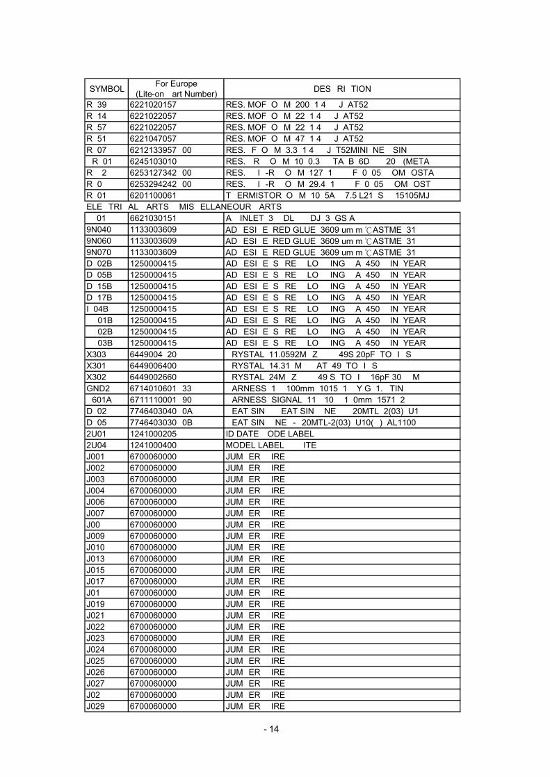
8- 14
SYMBOL For Europe(Lite-on Part Number) DESCRIPTION
R839 6221020157P RES. MOF_OHM_200_1/4W_J_AT52R814 6221022057P RES. MOF_OHM_22_1/4W_J_AT52R857 6221022057P RES. MOF_OHM_22_1/4W_J_AT52R851 6221047057P RES. MOF_OHM_47_1/4W_J_AT52R807 6212133957P00 RES.CF_OHM_3.3_1/4W_J_T52MINI_NEWSINVR801 6245103010P RES. VR_KOHM_10_0.3W_TA_B_6D_+/_20%(METAR882 6253127342P00 RES.CHIP-R_KOHM_127_1/8W_F_0805_COMPOSTAR808 6253294242P00 RES.CHIP-R_KOHM_29.4_1/8W_F_0805_COMPOSTR801 6201100061P THERMISTOR_OHM_10_5A_P7.5/L21_SCK15105MJELECTRICAL PARTS & MISCELLANEOUR PARTSP801 6621030151P AC INLET_3P_DLK_CDJ_3_GS/A9N040 1133003609P ADHESIVE_RED GLUE_3609 um/m/℃ASTME831_89N060 1133003609P ADHESIVE_RED GLUE_3609 um/m/℃ASTME831_89N070 1133003609P ADHESIVE_RED GLUE_3609 um/m/℃ASTME831_8D802B 1250000415P ADHESIVE_SCREW LOCKING_VA_450_PIN_YEARD805B 1250000415P ADHESIVE_SCREW LOCKING_VA_450_PIN_YEARD815B 1250000415P ADHESIVE_SCREW LOCKING_VA_450_PIN_YEARD817B 1250000415P ADHESIVE_SCREW LOCKING_VA_450_PIN_YEARI804B 1250000415P ADHESIVE_SCREW LOCKING_VA_450_PIN_YEARQ801B 1250000415P ADHESIVE_SCREW LOCKING_VA_450_PIN_YEARQ802B 1250000415P ADHESIVE_SCREW LOCKING_VA_450_PIN_YEARQ803B 1250000415P ADHESIVE_SCREW LOCKING_VA_450_PIN_YEARX303 6449004820P CRYSTAL_11.0592MHZ_HC_49S 20pF_TOPICSX301 6449006400P CRYSTAL_14.318MHz_AT_49_TOPICSX302 6449002660P CRYSTAL_24MHZ_HC_49/S_TOPIC_16pF 30PPMGND2 6714010601P33 HARNESS_1P_100mm_1015#18_Y/G_1.8/TINP601A 6711110001P90 HARNESS_SIGNAL_11P/10P_180mm_1571#28D802C 7746403040P0A HEAT SINK_HEAT SINK_NEC_C20MTL_2(03)~U1D805C 7746403030P0B HEAT SINK_NEC-C20MTL-2(03)~U10(C)_AL11002U01 1241000205P ID DATE CODE LABEL2U04 1241000400P MODEL LABEL_WHITEJ001 6700060000P JUMPER WIREJ002 6700060000P JUMPER WIREJ003 6700060000P JUMPER WIREJ004 6700060000P JUMPER WIREJ006 6700060000P JUMPER WIREJ007 6700060000P JUMPER WIREJ008 6700060000P JUMPER WIREJ009 6700060000P JUMPER WIREJ010 6700060000P JUMPER WIREJ013 6700060000P JUMPER WIREJ015 6700060000P JUMPER WIREJ017 6700060000P JUMPER WIREJ018 6700060000P JUMPER WIREJ019 6700060000P JUMPER WIREJ021 6700060000P JUMPER WIREJ022 6700060000P JUMPER WIREJ023 6700060000P JUMPER WIREJ024 6700060000P JUMPER WIREJ025 6700060000P JUMPER WIREJ026 6700060000P JUMPER WIREJ027 6700060000P JUMPER WIREJ028 6700060000P JUMPER WIREJ029 6700060000P JUMPER WIRE
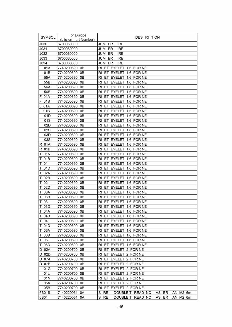
8- 15
SYMBOL For Europe(Lite-on Part Number) DESCRIPTION
J030 6700060000P JUMPER WIREJ031 6700060000P JUMPER WIREJ032 6700060000P JUMPER WIREJ033 6700060000P JUMPER WIREJ034 6700060000P JUMPER WIREC801A 7740200690P0B RIVET_EYELET_1.6_FOR NEC801B 7740200690P0B RIVET_EYELET_1.6_FOR NEC855A 7740200690P0B RIVET_EYELET_1.6_FOR NEC855B 7740200690P0B RIVET_EYELET_1.6_FOR NEC856A 7740200690P0B RIVET_EYELET_1.6_FOR NEC856B 7740200690P0B RIVET_EYELET_1.6_FOR NEF801A 7740200690P0B RIVET_EYELET_1.6_FOR NEF801B 7740200690P0B RIVET_EYELET_1.6_FOR NEL801A 7740200690P0B RIVET_EYELET_1.6_FOR NEL801B 7740200690P0B RIVET_EYELET_1.6_FOR NEQ801D 7740200690P0B RIVET_EYELET_1.6_FOR NEQ801S 7740200690P0B RIVET_EYELET_1.6_FOR NEQ802D 7740200690P0B RIVET_EYELET_1.6_FOR NEQ802S 7740200690P0B RIVET_EYELET_1.6_FOR NEQ803D 7740200690P0B RIVET_EYELET_1.6_FOR NEQ803S 7740200690P0B RIVET_EYELET_1.6_FOR NER801A 7740200690P0B RIVET_EYELET_1.6_FOR NER801B 7740200690P0B RIVET_EYELET_1.6_FOR NET801A 7740200690P0B RIVET_EYELET_1.6_FOR NET801B 7740200690P0B RIVET_EYELET_1.6_FOR NET801C 7740200690P0B RIVET_EYELET_1.6_FOR NET801D 7740200690P0B RIVET_EYELET_1.6_FOR NET802A 7740200690P0B RIVET_EYELET_1.6_FOR NET802B 7740200690P0B RIVET_EYELET_1.6_FOR NET802C 7740200690P0B RIVET_EYELET_1.6_FOR NET802D 7740200690P0B RIVET_EYELET_1.6_FOR NET803A 7740200690P0B RIVET_EYELET_1.6_FOR NET803B 7740200690P0B RIVET_EYELET_1.6_FOR NET803C 7740200690P0B RIVET_EYELET_1.6_FOR NET803D 7740200690P0B RIVET_EYELET_1.6_FOR NET804A 7740200690P0B RIVET_EYELET_1.6_FOR NET804B 7740200690P0B RIVET_EYELET_1.6_FOR NET804C 7740200690P0B RIVET_EYELET_1.6_FOR NET804D 7740200690P0B RIVET_EYELET_1.6_FOR NET806A 7740200690P0B RIVET_EYELET_1.6_FOR NET806B 7740200690P0B RIVET_EYELET_1.6_FOR NET806C 7740200690P0B RIVET_EYELET_1.6_FOR NET806D 7740200690P0B RIVET_EYELET_1.6_FOR NED802A 7740200700P0B RIVET_EYELET_2_FOR NED802D 7740200700P0B RIVET_EYELET_2_FOR NED807A 7740200700P0B RIVET_EYELET_2_FOR NED807B 7740200700P0B RIVET_EYELET_2_FOR NEP801G 7740200700P0B RIVET_EYELET_2_FOR NEP801L 7740200700P0B RIVET_EYELET_2_FOR NEP801N 7740200700P0B RIVET_EYELET_2_FOR NEP805A 7740200700P0B RIVET_EYELET_2_FOR NEP805B 7740200700P0B RIVET_EYELET_2_FOR NE6B01S 7140220061P0A SCREW_DOUBLE THREAD_NO WASHER_PAN_M2_6m6B01V 7140220061P0A SCREW_DOUBLE THREAD_NO WASHER_PAN_M2_6m

8- 16
SYMBOL For Europe(Lite-on Part Number) DESCRIPTION
D802A 7116230082P0A SCREW_MACHINE_STAR_WASHER_PAN_M3_8L_NID805A 7116230082P0A SCREW_MACHINE_STAR_WASHER_PAN_M3_8L_NID815A 7116230082P0A SCREW_MACHINE_STAR_WASHER_PAN_M3_8L_NID817A 7116230082P0A SCREW_MACHINE_STAR_WASHER_PAN_M3_8L_NII804A 7116230082P0A SCREW_MACHINE_STAR_WASHER_PAN_M3_8L_NIQ801A 7116230082P0A SCREW_MACHINE_STAR_WASHER_PAN_M3_8L_NIQ802A 7116230082P0A SCREW_MACHINE_STAR_WASHER_PAN_M3_8L_NIQ803A 7116230082P0A SCREW_MACHINE_STAR_WASHER_PAN_M3_8L_NIQ802C 7740201220P0A NUT-STANDARD NUT-FLANGE HEX NUTS1 7742612430P0A SUPPORT_PCB_PINGOOD_NYLON 94V0_NATURE_S2 7742612430P0A SUPPORT_PCB_PINGOOD_NYLON 94V0_NATURE_S3 7742612430P0A SUPPORT_PCB_PINGOOD_NYLON 94V0_NATURE_S4 7742612430P0A SUPPORT_PCB_PINGOOD_NYLON 94V0_NATURE_S5 7742612430P0A SUPPORT_PCB_PINGOOD_NYLON 94V0_NATURE_S6 7742612430P0A SUPPORT_PCB_PINGOOD_NYLON 94V0_NATURE_S601 6853011200P40 SWITCH_TACT_EVQWHA50K_PANASONICSW301 6853010800P SWITCH_TACT_SFKQYMA2250T_FORWARD_SMDSW601 6853001100P SWITCH_TACT_SKHHAK2510_BLK 5mmSW602 6853001100P SWITCH_TACT_SKHHAK2510_BLK 5mmSW603 6853001100P SWITCH_TACT_SKHHAK2510_BLK 5mmSW604 6853001100P SWITCH_TACT_SKHHAK2510_BLK 5mmT804 6131022400P XFRMER_POWER_TPW_1141_ER2819_LSE PLI5005T801 6131031700P XFRMER_POWER_TPW-1142_ER2843_LSE_PLI5006T806 6131043600P XFRMER_POWER_TPW-1143_ER2834_LSE/PLI5007MECHANICAL ASSY6B01R 7742611313P0A COVER_NMV_#6700+#6700P_PC+ABS 94V06B01T 7742611303P0A COVER_NMV_#6700+#6700P_PC+ABS 94V06B01M 7742611330P0A COVER_LENS COVER_NMV_NMV_A20BAL_PISA 206B01N 7742807581P0A PUSH BUTTON_#6700/#6700P_PC+ABS 94V0_6B01Q 7742807293P0B PUSH BUTTON_4 AXIS KNOB_#6700/#6700P_6B01P 7742302550P0A LENS_POWER_NMV_NMV_A20BAL_PISA 20_TRANS6L01A 7742611931P0A COVER_TERMINAL BOTTOM COVER_#6700_PC+ABS6L01C 7746204170P0A SHIELD_USB SHIELD COVER_NEC_C20MTL_2(036L01F 7110330062P0A SCREW-MACHINE-FLAT HEAD-M3-6-NI6L01G 7110330062P0A SCREW-MACHINE-FLAT HEAD-M3-6-NI6L01H 7116240081P0A SCREW-MACHINE-Star Washer-Pan-M4-8-Zn6L01I 7740201240P0A SCREW_MACHINE_FLAT WASER_PAN_M3_6L_Z6L01J 7740201240P0A SCREW_MACHINE_FLAT WASER_PAN_M3_6L_Z6L01K 7746503720P0A INSULATOR_NEC_C20MTL_2(03)~U10(C)_PPE_I6L01L 7110340102P0A SCREW_MACHINE_NONE_FLAT HEAD_M4_10_N6L01M 7140226122P0A SCREW_DOUBLE THREAD_WITHOUT WASHER_PAN6L01O 7740200890P SCREW_Cu-Ni06B01 7737609551P0A RC ASSY_KAMA 20 WS_#6700_PC+ABS UL-94V0_6BA1 7742233051P0A RC_NMV_KAMA 20 WS_#6700_PC+ABS 94V0_6BB1 7742611921P0A RAIL_CENTER CABINET_#6700_PC+ABS 94V0_6BC1 7140130061P0A SCREW_MACHINE_WITHOUT_NINDING_M3_6L_BLA6BD1 7748711550P0A BRACKET_SPEAKER BRACKETL_NEC_C20MTL_2(06BE1 7748711560P0A BRACKET_SPEAKER BRACKETR_NEC_C20MTL_2)06BF1 7140330082P0A SCREW-MACHINE-NONE-FLAT HEAD-M3-8-NI8C01 7737710453P0A BASE ASSY_#6700_PC+ABS 94V0_NMV_U20BNL8CA1 7738000861P0A HINGE_HINGE TILT ASSY_NMV_20_SECC_8CB1 7742612111P0A COVER_HINGE COVER(NEC)_#6700_PC+ABS 94V0
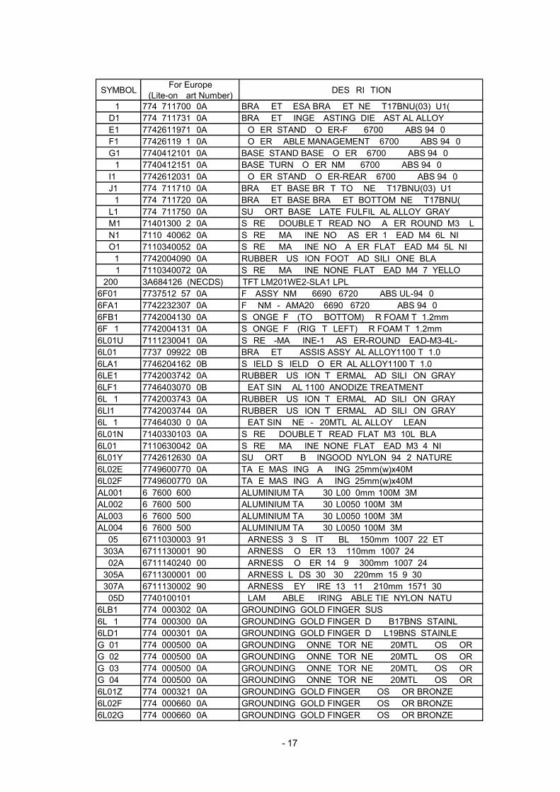
8- 17
SYMBOL For Europe(Lite-on Part Number) DESCRIPTION
8CC1 7748711700P0A BRACKET_VESA BRACKET_NEC_T17BNU(03)~U1(8CD1 7748711731P0A BRACKET_HINGE CASTING_DIE CAST AL ALLOY_8CE1 7742611971P0A COVER_STAND COVER-FC_#6700_PC+ABS 94V08CF1 7742611981P0A COVER_CABLE MANAGEMENT_#6700_PC+ABS 94V08CG1 7740412101P0A BASE_STAND BASE COVER_#6700_PC+ABS 94V08CH1 7740412151P0A BASE_TURN COVER_NMV_#6700_PC+ABS 94V08CI1 7742612031P0A COVER_STAND COVER-REAR_#6700_PC+ABS 94V08CJ1 7748711710P0A BRACKET_BASE BRKT_TOP_NEC_T17BNU(03)~U18CK1 7748711720P0A BRACKET_BASE BRACKET_BOTTOM_NEC_T17BNU(8CL1 7748711750P0A SUPPORT_BASE PLATE_FULFIL_AL ALLOY_GRAY8CM1 7140130082P0A SCREW_DOUBLE THREAD_NO WAHER_ROUND_M3_8L8CN1 7110840062P0A SCREW_MACHINE_NO WASHER_1 HEAD_M4_6L_NI8CO1 7110340052P0A SCREW_MACHINE_NOWAHER_FLAT HEAD_M4_5L_NI8CP1 7742004090P0A RUBBER CUSHION_FOOT PAD_SILICONE_BLACK8CQ1 7110340072P0A SCREW_MACHINE_NONE_FLAT HEAD_M4_7_YELLOV200 3A6841268(NECDS) TFT LM201WE2-SLA1 LPL6F01 7737512857P0A FC ASSY_NMV_#6690/#6720_PC+ABS UL-94V0_6FA1 7742232307P0A FC_NMV-KAMA20_#6690/#6720P_PC+ABS 94V0_6FB1 7742004130P0A SPONGE_F/C(TOP&BOTTOM)_CR FOAM T=1.2mm6FC1 7742004131P0A SPONGE_F/C(RIGHT&LEFT)_CR FOAM T=1.2mm6L01U 7111230041P0A SCREW-MACHINE-1 WASHER-ROUND HEAD-M3-4L-6L01 7737809922P0B BRACKET_CHASSIS ASSY_AL ALLOY1100 T=1.0_6LA1 7746204162P0B SHIELD_SHIELD COVER_AL ALLOY1100 T=1.0_6LE1 7742003742P0A RUBBER CUSHION_THERMAL PAD_SILICON_GRAY6LF1 7746403070P0B HEAT SINK_AL 1100_ANODIZE TREATMENT_6LH1 7742003743P0A RUBBER CUSHION_THERMAL PAD_SILICON_GRAY6LI1 7742003744P0A RUBBER CUSHION_THERMAL PAD_SILICON_GRAY6LK1 7746403080P0A HEAT SINK_NEC-C20MTL_AL ALLOY_CLEAN_6L01N 7140330103P0A SCREW_DOUBLE THREAD_FLAT_M3_10L_BLACK6L01V 7110630042P0A SCREW_MACHINE_NONE_FLAT HEAD_M3_4_NI6L01Y 7742612630P0A SUPPORT_PCB_PINGOOD_NYLON_94V2_NATURE_6L02E 7749600770P0A TAPE_MASKING PACKING_25mm(w)x40M_6L02F 7749600770P0A TAPE_MASKING PACKING_25mm(w)x40M_AL001 6876008600P ALUMINIUM TAP_W30*L0080mm*100M_3MAL002 6876008500P ALUMINIUM TAP_W30*L0050*100M_3MAL003 6876008500P ALUMINIUM TAP_W30*L0050*100M_3MAL004 6876008500P ALUMINIUM TAP_W30*L0050*100M_3MP805C 6711030003P91 HARNESS_3P/SWITCH BLK_150mm_1007#22_ETP303A 6711130001P90 HARNESS_POWER_13P_110mm_1007#24P802A 6711140240P00 HARNESS_POWER_14P/9P_300mm_1007#24P305A 6711300001P00 HARNESS_LVDS_30P/30P_220mm_1589#30P307A 6711130002P90 HARNESS_KEY WIRE_13P/11P_210mm_1571#30P805D 7740100101P CLAMP_CABLE_WIRING CABLE TIE_NYLON_NATU6LB1 7748000302P0A GROUNDING_GOLD FINGER_SUS_6LC1 7748000300P0A GROUNDING_GOLD FINGER_DCC_B17BNS_STAINL6LD1 7748000301P0A GROUNDING_GOLD FINGER_DCCL19BNS_STAINLEG801 7748000500P0A GROUNDING_CONNECTOR_NEC_C20MTL_PHOSPHORG802 7748000500P0A GROUNDING_CONNECTOR_NEC_C20MTL_PHOSPHORG803 7748000500P0A GROUNDING_CONNECTOR_NEC_C20MTL_PHOSPHORG804 7748000500P0A GROUNDING_CONNECTOR_NEC_C20MTL_PHOSPHOR6L01Z 7748000321P0A GROUNDING_GOLD FINGER_PHOSPHOR BRONZE_6L02F 7748000660P0A GROUNDING_GOLD FINGER_PHOSPHOR BRONZE_6L02G 7748000660P0A GROUNDING_GOLD FINGER_PHOSPHOR BRONZE_
8- 18
SYMBOL For Europe(Lite-on Part Number) DESCRIPTION
PACKING ASSY1P11 7749205948P0A CARTON_NEC_U20BN_20WGX2(B-BK)_720SETS1P21 7749105560P0A CUSHION FOAM_EPS_KAMA-20SV_720SETS_T&B_1P31 7749002100P0A BAG_LDPE+EPE_ORDINARY_FOR HP_850(l)*6501P33 7749001360P0B BAG_LLDPE_ORDINARY_ALL MODEL_W500mm*H0.1P34 7749001370P0A BAG_LLDPE_FILM STRETCH WRAP_ALL MODEL_W1P42 7749600470P0A TAPE_PACKING_914Mx76mmx0.066mm_FOR DELL1P43 7749600200P0A TAPE_MASKING_PACKING_25mm(w)x45m_LITEON1P44 7749600650P0A TAPE_PACKING_250Mx15mmx0.95mm_ALL MODEL1P51 7749402250P0A BOARD_CORNER PAPER_1200*50*3mm_H1P52 7749405180P0A BOARD_CORNER PAPER_1030*50*3mm_H1P53 7749401980P0A BOARD_CORNER PAPER_L2050xW50x3mm1P56 7749405320P0A PAPER BOARD_1300*1100*4mm_ALL MODE1P71 7749502450P0A PALLET_FOUR WAY_1320*1145*115h_NM2B01 7735430565P0A LABEL_MODEL LB_NEC_U20BN_BLK_154x51mm_2P09 7735419260P PACKING LABEL_ALL_ALL_WHITE_297*210Y001 7730302952P0A MANUAL ASSY_NEC-DS_U20BNL_20WGX2-L205GJ_Y0A1 7730114002P0A MANUAL_NEC-DS_U20BNL_20WGX2-L205GJ_EMEAY0B1 7730203293P0A CARD_CD MANUAL_NEC-DS_U20BNL_EMEA_Y0C1 7730203214P0A CARD-NAVISET FLYER-NMV-NAVISETFLYER04140Y0D1 7730203216P0A CARD_SALES OFFICE LIST CARD_NMV_SALES O1P45 7749600770P0A TAPE_MASKING PACKING_25mm(w)x40M_1P57 7749405360P0A PAPER BOARD_555*247_NM2P01 7735428510P0A PACKING LABEL_NMV_NX76(L172EN)_MTS_B17BPC01 6716004835P CABLE_POWER_TO WALL_2000mmV001 6715008208P00 CABLE_VIDEO_D-SUB*2_2000mm_BLK_JCEV002 6715009005P00 CABLE_VIDEO_DVI-D*2_2000mm_BLK_JCEV003 6710010186P CABLE_USB A+B_2000mm_BLK_USB 2.0Y002 7730202345P0A CARD_CAUTION SHEET_NMV_A21BNS_EMEA_NEC_Y003 7730203294P0A CARD_SETUP CARD_NEC-DS_U20BNL_EMEA_
9-1
NEC-20WGX2 Block Diagram
VGAP301
DVIP302
OAKGENESISgm5861-LF
Display Scaler
I308
I303
VGA-EDID
I334
PC-EDID
MuxI333
TMDS Signal
Analog-RGB
I311SDRAM1M*16
I311SDRAM1M*16
I309SPI
Flash
I310
NVRAM
I325 CPU
for <1W
USBP309 UpStream
USB P310Down Stream
CY7c65640A-LFC
PTB-1621Power Board
I3073.3VDCRegulator
I3061.8VDCRegulator
5VDC
PSU-ON-OFF
USB BD PTB-1605 Down Stream
PTB-1680
PTB-1671 KEY-PAD
PANEL 20" LPL LM201WE2-SLA1
AI-DCRI331/332/323
12VDC
LVDS OUTPUT
USB
I319
I328AO44075VDCSwitch
5VDC
5V ON/OFF
+5VDC
MODEL LCD 20WGX2 SCHEMATIC DIAGRAM - InputsPWR - Dsub/DVI (1/5)
10-1
High-33msec
TO263
TO263
SET LOW: Select DIM_OUT(Panel control)
SET HIGH: Select PWM_BRI(Scaler control)
AI_ENABLE:
BRI source select multiplexer forLPL panel only.
PIN_9
SCL_DVI
RED
DVI_CE
DDC_CLK
BLUE
GREEN
Hsync
DVI_PC
SDA_DVI
Vsync
PIN_10
DDC_DATA
0805
0805
ESD-111005
Pitch:1.0mm
6374210512P--MP s
tage.
CGND
+12VI
CGND
CGND
POWOFF
+12VI
CGND
+5VI
+5VI
BRI
INV_ENA
+5VI
POFF
POWOFF
uP_5V_OFF
uP_5V_OFF
DRXC+
DRX1+
WPDRX1-
+5V_DVI
DRXC+
DDC_SDA_DVI
WP
PC_SDA
WP
5V_DVI
DRX2+
CE_SCL
DRX2-
PC_SCL
DRXC-
DRX2-
CE_SDA
DRX0+
5V_DVI
DDC_SCL_DVI
DRX0-
DRXC-
DRX1-
DRX1+DRX2+
PAIRB
DRX0-DRX0+
BKLT_EN 3
PWM_BRI 3
DIM_OUT 4
MUTE 3
AI_ENABLE 3,4
PWRDOWN3
DDC_SCL_DVI 3
HSYNC13
VSYNC13
DDC_SDA_VGA3
DDC_SCL_VGA3
WP_EN3
VGA_CAB3
DVI_CAB 3
DDC_SDA_DVI 3
DVI_SW 3
uP_IR_RS7704
uP_KEY_PWR4
DPMS_SW3KEY_SW4
DVI_CTL 3
RX2- 3RX2+ 3
RX1- 3RX1+ 3
RX0+ 3RX0- 3
RXC- 3RXC+ 3
RED+3
GREEN+3
BLUE+3
GND
GND
+5V
5V
+5V
+5V
+5V
GND
GND
GND GND
GND
GND
GND
GND+12V
GND
GND
+5V
GND
5V
5V
GND
GND
+3_3AVDD
GND
+1_8DVDD
GND
GND
5160_1_8V+5V+3_3DVDD
+1_8AVDD
GND
GND
GND
SGND
SGND
SGND
GND
SGND
+5V
SGND
+5V
+5V
+5V
SGND
+5V
SGND
GND
GND
+5V
GND
GND
GND
SGND
SGND
GND
SGND
SGND
+5V
+5V
SGND
SGND
GND
GND
SGND
SGND
GNDSGND
SGND
GND
GND
+3_3DVDD
GND
SGND
+5V
GND
GND
FB307SBK160808T-060YS
R331 10K
C33
40.
1uF
R307 100
R334 3K3
I328AO4407
1
2
3
4
5
6
7
8
R519 10R
C319
47pF
R318100
C33
2N
C
R315
47K
R329 4K7
D315RLS4148
2 1
P303A2501WR2-13P
1
2
3
4
5
6
7
8
9
10
11
12
13
R324 20
D312ZD5.6B
2 1
D311 RLS41482 1
R338 10K
R504
4K7
Q323MMBT3904 2
13
C312
47pF
C32
3N
C
R32310K
Q322MMBT3906
2
3 1
R522 10R
D316MMBD7000
3
1 2
D317 RLS41482 1
D314 ZD5.6B2 1
R313 100
C523 1uF/16V
R4894K7F
C52
21u
F/1
6V 0
805
C313 1uF/16V
R317100
C35
90.
1uF
Q32
1
MM
BT
3904
3
2
1
D310 ZD5.6B21
D32
5M
MB
D70
00
21
3
C34
31u
F/1
6V
C33
70.
1uF
Q324MMBT3906
2
13
I334 24LC02B1
2
3
45
6
7
8A0
A1
A2
VSSSDA
SCL
WP
VCC
D30
3Z
D5.
6B2
1
-
+
I332ALMV358
3
21
84
R51010K
D32
2M
MB
D70
00
21
3
R469 0
R515 10RC527
0.1uF
D309 ZD5.6B2 1
D306 ZD5.6B21
TP204
R521 10R
C325 0.1uF
-
+
I332BLMV358
5
67
84
C5111uF/16V
R493 3K3
D313 RLS414821
C51622pF
FB316PBY201209T-300Y-S
C525
47pF
FB313PBY201209T-300Y-S
R326 20
D308RLS4148
2 1
C36
222
0uF
/10V
I326A74HC14
1 2
147
C318
47pF
C324 0.1uF
C317 0.1uF
R508 22
I324NC7SZ04
2 4
53
C5154.7uF/16V-1206
I326D74HC14
9 8
R32
575
C36
10.
1uFQ304
MM
BT
3906
2
3 1
R478 22
C33
60.
1uF
FB302 BK2125HS431
C307
0.1uF
R4994K7
FB315PBY201209T-300Y-S
R47510K
C308
10pF
Q326MMBT3904
2
13
R47
410
K
R506 47
C32
80.
1uF
C34
60.
1uF
I333 74LV4052_NS
9
5
14
10
4
1
12
118
16
7
6
23
13
15
S1
A1
B1
S0
A3
A0
B0
B3GND
VCC
GND
OE
A2YAYB
B2
R32
775
I323 74LV4052_NS
9
5
14
10
4
1
12
118
16
7
6
23
13
15
S1
A1
B1
S0
A3
A0
B0
B3GND
VCC
GND
OE
A2YAYB
B2
D318 MMBD7000
3
1 2
C33
50.
1uF
R332 100
C344
0.1uF
D30
4Z
D5.
6B2
1
R320 47
R3373K3
R482120F
FB303PBY201209T-300Y-S
I326B74HC14
3 4
C301 1uF/16V
R305
47K
C518
0.1uF
C302 0.1uF
R49
78K
2F
R308
2K2
C3310.1uF
R5094K7
FB308SBK160808T-101YS
Q301
MMBT39042
13
R311 47
C52
10.
1uF
R314 100
R516 10R
R47610K
R322100
R309
2K2
R490 4K7
FB321PBY201209T-300Y-S
C314
0.1uF
C34
10.
1uF
FB314PBY201209T-300Y-S
C327 0.1uF
R505 47
C524 0.1uF
C526
47pF
R501 3K3
P301
VGA DB15
DIP TYPE
815
714
613
512
411
310
291
FB317PBY201209T-300Y-S
R491 4K7
C305
0.1uF
D321 MMBD7000
3
1 2
C531 1uF/16V
C33
80.
1uF
R312 3K3
C35
622
0uF
/10V
D307 RLS414821
C530
2.2uF
D333 SS14
21
D32
4M
MB
D70
00
21
3
C315 0.1uF
R487
4K7
FB310SBK160808T-101YS
FB304PBY201209T-300Y-S
TP205
R3363K3
R518 10R
Q302MMBT3904
3
2
1
P302DVI-D
123456789101112131415161718192021222324
RX2-RX2+GNDRX4-
RX4+SCLSDA
NCRX1-
RX1+GNDRX3-
RX3+5V
GNDHP
RX0-RX0+GNDRX5-
RX5+GND
RXC+RXC-
I325
SM89516C25JA
35
21
20
10
14151617
23456789
4342414039383736
2425262728293031
191832331311
44221 23 3412
EA
/VPXTAL1
XTAL2
RST
INT0/P3.2INT1/P3.3TO/P3.4T1/P3.5
T2/P1.0T2EX/P1.1P1.2P1.3P1.4P1.5P1.6P1.7
P0.0/AD0P0.1/AD1P0.2/AD2P0.3/AD3P0.4/AD4P0.5/AD5P0.6/AD6P0.7/AD7
P2.0/A8P2.1/A9
P2.2/A10P2.3/A11P2.4/A12P2.5/A13P2.6/A14P2.7/A15
RD/P3.7WR/P3.6
PSENALE/PROG
TXD/P3.1RXD/P3.0
VC
CG
ND
NC
NC
NC
NC
C329 0.1uF
FB324PBY201209T-300Y-S
FB305PBY201209T-300Y-S
R502
47K
C333 0.1uF
FB301 BK2125HS431
D32
7M
MB
D70
00
21
3
R47
71M
FB312PBY201209T-300Y-S
D32
9M
MB
D70
00
21
3
C51
70.
56uF
R47
310
K
R339 470
FB311SBK160808T-060YS
C5120.1uF
R49
610
KF
Q325MMBT3904
3
2
1
C316
0.1uF
I307 LM1085IS-ADJ
1
234
AD
J
VOUTVINSink
X30
3
11.0
592M
Hz
R34
010
K
D301RLS4148
21
D302ZD5.6B
21
R485
12K
C321 0.1uF
D320 MMBD7000
3
1 2
R517 10R
C36
022
0uF
/10V
R333 20
C51
40.
1uF
D305RLS4148
21
C35
50.
1uF
R483 200F
C32
6N
C
C33
90.
1uF
R330 10K
C51
00.
1uF
I326C74HC14
5 6
I304 24LC02B1
2
3
45
6
7
8 A0
A1
A2
VSSSDA
SCL
WP
VCC
C33010nF
R49210KF
Q32
7M
MB
T39
06
2
13
FB309SBK160808T-060YS
C309
47pF
R5003K3
D32
6M
MB
D70
00
21
3
C34
20.
1uF
C51322pF
C509
0.1uF
R49410KF
R503
47K
I303 24LC02B1
2
3
4 5
6
7
8A0
A1
A2
VSS SDA
SCL
WP
VCC
R303
4K7
FB325PBY201209T-300Y-S
TP
203
D32
3M
MB
D70
00
21
3
C303
0.1uF
D32
8M
MB
D70
00
21
3
C35
30.
1uF
R498 3K3F
R484 56F
I306 LM1085IS-ADJ
1
234
AD
J
VOUTVINSink
R4862K2
Q303MMBT3906
2
13
FB322PBY201209T-300Y-S
R4886K8F
C34
722
0uF
/25V
R520 10R
C532 1uF/16V
I331MMDT3904
241
56
3
B2E1E2
B1C2
C1
R319 100
D319 MMBD7000
3
1 2
R302 100
C311
47pF
R32
810
K
R316
47K
C34
00.
1uF
R481120F
C310
47pF
R321 47
R495 10KF
C304
10nF
R310 47
C320
0.1uF
C322 0.1uF
R33
575
FB306SBK160808T-101YS
R50
73K
3F
R304
47K
+12V 4
+3_3AVDD 3 +1_8DVDD 3
+1_8AVDD 3
5160_1_8V 4+5V 3,4,5 +3_3DVDD 3,4
5V 4

MODEL LCD 20WGX2 SCHEMATIC DIAGRAM - Scaler FLI5961H/gm5861 (2/5)
10-2
DQ_B_4
DQ_B_8
DQ_A_4
DQ_B_2
DQ_B_13
LV_O6
DQ_B_6
DQ_A_11
DQ_B_[0..15]
GPIO_1
LV_E5
V_5160_D5
LV_O2
SPI_CSn-BOOT0
SPI_DO-BOOT2DQ_A_14
DDC_SDA_VGA
DQ_B_15
LV_O[0..9]
DQ_B_1
LV_E2
DQ_B_14
DQ_A_3
LV_O1
DQ_B_0
SPI_DO-BOOT2
DQ_B_5
LV_E4
DQ_A_[0..15]
LV_E8
PWM1-BOOT4
LV_O8
SDA
LV_E6
DQ_A_10
SPI_DI
UART_DO-BOOT3
LV_E1
V_5160_D4
DQ_B_12V_5160_D7
SDA
LV_E3
SPI_CLK-BOOT1
LV_O3
LV_O9
LV_O5
DQ_A_2
LV_O7
V_5160_D[0..7]
DQ_A_7DQ_A_6
SPI_CSn-BOOT0
PWM0-BOOT5
DQ_A_1
GPIO_9/PWM3/BOOT7
LV_O0
DQ_A_15
V_5160_D0
DQ_A_9
LV_E0
V_5160_D3
LV_E[0..9]
DQ_A_5
DQ_A_8
DQ_A_13
V_5160_D1
GPIO_0
DQ_B_11
GPIO_8/PWM2/BOOT6
DQ_B_3
DQ_B_9
LV_E9
V_5160_D6
LV_O4
DDC_SCL_VGA
DQ_B_10
LV_E7
SPI_CLK-BOOT1
RESETn
V_5160_D2
GPIO_9/PWM3/BOOT7
DQ_A_0
DQ_B_7
DQ_A_12
GPIO_8/PWM2/BOOT6
DPWON
PWM0-BOOT5
BKLT_EN
RESETn
PWM1-BOOT4
IR_RS770
VIN1VIN2
UART_DI
SCL
5160_IRQ
MUTE
SPI_WP
SPI_WP
SCL
UART_DO-BOOT3
A10A0
A6
A[0..10]
A9A8
A5
A1
A7
A2A3A4
RX1-2
DQ_B_[0..15] 4
A[0..10] 4
WEn 4
RX2-2
LV_E[0..9] 4
LV_O[0..9] 4
RX1+2
RX0+2
RASn 4CASn 4
RXC+2
DDC_SCL_DVI2
DQM 4
DDC_SCL_VGA2
RXC-2
DDC_SDA_VGA2
BKLT_EN 2
MCLK 4
DDC_SDA_DVI2
BA 4
RX0-2
RX2+2
5160_CLK4
V_5160_D[0..7]4
D4_114
DPWON 4
WP_EN 2DVI_CAB 2VGA_CAB 25V_T_EN 4
PWRDOWN 2
IR_RS770 4
5160_PWDN 4
KEY_PWR4
VIN14VIN24
RED+2
BLUE+2
GREEN+2
Pb4
Y4Pr4
VSYNC12HSYNC12
USB_EN 5
SDA 4SCL 4
5160_IRQ 4
MUTE 2
PWM_BRI 2LED_AMBER 4LED_BLUE 4
Resetb4
LED_BLUE_ADJ 4
AI_ENABLE 2,4
Audio_In_Sel4
DVI_CTL 2DVI_SW 2
DQ_A_[0..15] 4DPMS_SW2
+1_8AVDD+1_8DVDD
+3_3AVDD +3_3ADCV
GND
+5V
GND
GND
GND
GND
+3_3AVDD 3_3AVDD
3_3AVDD
+3_3ADCV
+3_3DVDD
+3_3DVDD
+3_3DVDD
+3_3DVDD
+3_3AVDD
+3_3RVDD
+3_3RVDD
GND
GND
GND
GND
GND
GND
GND
GND
GND
+5V
GND
GND
GND
+3_3ADCV
+5V
+3_3RVDD
GND
+3_3DVDD+3_3RVDD
+3_3RVDD
SW301
R376 22
RN3090Rx4
1234 5
678
R37010K
R34
410
K
R3496K
FB330PBY201209T-300Y-S
TP3SCL Pogo
R355 56 1%
R373 10K
C397
0.1uF
C389
0.1uF
C379
0.1uF
R37
8N
CC412
0.1uF
RN3040Rx4
1234 5
678
C407
10nF
RN3070Rx4
1234 5
678
C408 10nF
TP4SDA Pogo
SP8
R379 22
FB331PBY201209T-300Y-S
RN3100Rx4
1234 5
678
RN3020Rx4
1234 5
678
C383
47uF/25V
C374
0.1uF
C409 10nF
C400
0.1uF
R34
8N
C
C390
0.1uFC401
0.1uF
SP1
C369
0.1uF
TP5GND Pogo
R380 22
R363 10K
C375
0.1uF
C396
0.1uF
C366
0.1uF
R45713.7K
C387
0.1uF
SP3
R358 10K
I310
24LC32B
1234 5
678A0
A1A2VSS SI
SCKWP
VCC
RN3050Rx4
1234 5
678
R366NC
C394
47uF/25V
RN3080Rx4
1234 5
678
R356 56 1%
RN3030Rx4
1234 5
678
TP15V Pogo
RN3110Rx4
1234 5
678
R350 0
R34
5N
C
I309
SST25VF040-20-4C-QAE
1234 5
678
CE#SOWP#VSS SI
SCKHOLD#
VCC
C392
0.1uF
C368
0.1uF
C398
0.1uF
C384
0.1uF
SP4
C40347uF/25V
R36910K
FB327
PBY201209T-300Y-SC376
0.1uF
C367
0.1uF
R364 10K
C378
0.1uF
R37110K
P304CON4
1234
R374 22
I308
FLI5961
8
1234567
9101112131415
16
17
1819202122
23
24
25
26272829303132333435
36
37
3839404142434445
4647484950515253
5455
56
57
5859
60
61
62
63646566676869707172
73
74
75767778798081828384
85
86
87888990
91
92 93
94959697
9899100101
102
103
104
105
106
107
108
109110
111
112113
114
115
116
117118
119
120121
122
123
124125
126
127
130131
132133
134
135
136137
138
139
140
141142
143
144
145
146147148
149
150
151
152153
154
155
156
157
158
159
160
161
162163
164
165
166
167168169
170
171
172
173
174
175
176177178179180181182183184
185
186
187188189190
191192
193
194
195
196
197198199200
201202203204
205
206
207
208
128129
DQ15_A
DQ6_ADQ5_ADQ4_ADQ3_ADQ2_ADQ1_ADQ0_A
DQ14_ADQ13_ADQ12_ADQ11_ADQ10_A
DQ9_ADQ8_A
CR
VS
S
RV
DD
_3.3
WE#CAS#RAS#
BAMCLK
A9
CR
VS
S
RV
DD
_3.3
A8A7A6A5A4A3A2A1A0
A10
RV
DD
_3.3
CR
VS
S
DQ7_BDQ6_BDQ5_BDQ4_BDQ3_BDQ2_BDQ1_BDQ0_B
DQ15_BDQ14_BDQ13_BDQ12_BDQ11_BDQ10_B
DQ9_BDQ8_B
RV
DD
_3.3
CV
DD
_1.8
CR
VS
S
DQM
PPWRPBIAS
AV
DD
_LV
_3.3
AV
SS
_LV
AV
DD
_OU
T_L
V_3
.3
CH3P_LV_E/R0CH3N_LV_E/R1CLKP_LV_E/R2CLKN_LV_E/R3CH2P_LV_E/R4CH2N_LV_E/R5CH1P_LV_E/R6CH1N_LV_E/R7CH0P_LV_E/G0CH0N_LV_E/G1
AV
SS
_OU
T_L
V
AV
DD
_OU
T_L
V_3
.3
CH3P_LV_O/G2CH3N_LV_O/G3CLKP_LV_O/G4CLKN_LV_O/G5CH2P_LV_O/G6CH2N_LV_O/G7CH1P_LV_O/B0CH1N_LV_O/B1CH0P_LV_O/B2CH0N_LV_O/B3
AV
SS
_OU
T_L
V
AV
DD
_OU
T_L
V_3
.3
GPIO_10/B4GPIO_11/B5GPIO_12/B6GPIO_13/B7
CR
VS
S
CV
DD
_1.8
RV
DD
_3.3
GPIO_14/DCLKGPIO_15/DENGPIO_16/DHSGPIO_17/DVS
GPIO_18/SCL_0(2W_Mst)GPIO_19/SDA_0(2W_Mst)GPIO_20/SCL_1(2W_Mst)GPIO_21/SDA_1(2W_Mst)
CV
DD
_1.8
CR
VS
S SCAN_EN
VS
SA
_DV
I
REXT
VDD_DVI_1.8
VS
SA
_DV
I
RX2+RX2-
VDDA_DVI_3.3
RX1+RX1-
VS
SA
_DV
I
VDD_DVI_1.8
VS
SA
_DV
I
RX0+RX0-
VDDA_DVI_3.3
RXC+RXC-
VS
S_D
VI
VDD_DVI_1.8
DDC_SCL_CH2DDC_SDA_CH2
CR
VS
S
RV
DD
_3.3
UART_DIUART_DO/BOOT[3]
HSYNC2VSYNC2
CV
DD
_1.8
CR
VS
S
HSYNC1VSYNC1
VS
SA
_AD
C
BLUE2+
VDDA_ADC_3.3
SOG_MCSS2GREEN2+
VS
SA
_AD
C
RED2+
VS
SA
_AD
C
BLUE-GREEN-RED-
VS
SA
_AD
C
BLUE1+
VDDA_ADC_3.3
SOG_MCSS1GREEN1+
VDDA_ADC_3.3
RED1+
VS
SA
_AD
C
GN
D1_
AD
C
VDD1_ADC_1.8
VBUFC_RPLL
VDD_RPLL_1.8
VS
S_R
PLL
XTALTCLK
AVDD_RPLL_3.3
RESETn
LBA
DC
_RT
N/G
ND
LBADC_IN3LBADC_IN2LBADC_IN1
LBA
DC
_VD
D_3
.3
JTAG_BS_EN
GPIO_22/INT1
CR
VS
S
CV
DD
_1.8
GPIO_23/INT0
GPIO_24/VD[0]GPIO_25/VD[1]GPIO_26/VD[2]GPIO_27/VD[3]GPIO_28/VD[4]GPIO_29/VD[5]GPIO_30/VD[6]GPIO_31/VD[7]VCLK
RV
DD
_3.3
CR
VS
S
SPI_CSn/BOOT[0]SPI_CLK/BOOT[1]SPI_DISPI_DO/BOOT[2]
GPIO_0/DDC_SCL_0GPIO_1/DDC_SDA_0
GPIO_2
GPIO_3/JTAG_RESET
CV
DD
_1.8
CR
VS
S
GPIO_4/JTAG_TDOGPIO_5/JTAG_TDIGPIO_6/JTAG_CLKGPIO_7/JTAG_MODE
PWM0/BOOT[5]PWM1/BOOT[4]
GPIO_8/PWM2/BOOT[6]GPIO_9/PWM3/BOOT[7]
CR
VS
S
CV
DD
_1.8
RV
DD
_3.3
DQ7_A
DDC_SCL_CH1DDC_SDA_CH1
C395
47uF/25V
R357 56 1%
SP2SP5
C404
0.1uF
RN3060Rx4
1234 5
678
R372 20K
C386
0.1uF
R354 10K
C371
0.1uF
X301
14.318MHz
C391
0.1uF
R34
6N
C
C385
0.1uF
SP6
R360 NC
C373
0.1uF
R368NC
R35
32K
2
C372
0.1uF
C399
0.1uF
R365 249 1%
C4110.1uF
C382
47uF/25V
R359 10K
C405
5.6pF
C388
0.1uF
R45
9N
C
SP7
C380
0.1uF
R37
7N
C
R456 3K3
R351 0
R35
22K
2
R375 33
C377
0.1uF
RN3010Rx4
1234 5
678
R361 10K
R34
7N
C
TP2Reset Pogo
C406
5.6pF
R362 NC
R458 10K
R455 3K3
C370
0.1uFC36547uF/25V
R36710K
C410 10nF
+3_3DVDD 2,4
+3_3AVDD 2
+1_8AVDD2+1_8DVDD2
GND
gProbe
DNP
Place each PogoPin Via withunobstructed vertical access.
NVRAM
R372
20K
D4_ADCR523 18KF4 D4_11
D connector issue
Reset BOOTSTRAP
GPIO9PWM1
Lo Int ROM selects TCLKLo 14.318MHz
Lo Int ROM selects TCLKHi 20MHz
Hi Int ROM selects TCLKLo 24MHz
Hi Int ROM selects TCLKHi 19.661MHz
Lo Hi
GPIO8
PWM0
U_DO
S_DO
Standard SPI i/f
OCM 20 bitADD mode
In ckt debug on DDC_D
Int OSC Ext OSC
Atmel Data Flash i/f
OCM 24 bitADD mode
In ckt debug on DDC_A
S_CLKS_CSn
Lo NormalLo
Lo DebugHi
Hi Test ALo
Hi Test B Hi
MODEL LCD 20WGX2 SCHEMATIC DIAGRAM - SDRAM & Panel outputs (3/5)
10-3
1st.K4S161622H-UC55, 183MHz, Samsung
TXOC+TXOC-
TXE0-
TXO3-
TXO2-
TXE1+
TXE0+
TXE2+
TXO1+
TXO0-
TXE3-TXE3+
TXE2-
TXEC-
TXO2+
TXO3+
TXO1-
TXEC+
TXE1-
TXO0+
12V for LG panel
5V for Samsungpanel
FB332
FB333
GND
IRSI
LED_A
GND
VIN1
ADC_VREFVIN2
ADC1_RETURN
ADC2_RETURN
LED_B
POWER_SW
+5V
MTS-C19MTS--6814902001P
NEC-C20MTL--6814200500P2nd.HY57V161610ETP-55,183MHz, Hynix3th.M12L16161A-5.5T, 183MHz, ESMT
del C519,Add R524
DQ_B_10
DQ_B_2
CASn
DQ_B_[0..15]
DQ_B_15DQ_B_0DQ_B_1
DQ_B_13DQ_B_3
CKE
DQ_B_8
BA
DQ_B_9
DQ_B_14
DQ_B_5
DQ_B_7
DQ_B_4
WEn
DQ_B_12
DQ_B_6
RASnCSn
DQ_B_11
A10
A1A2
A10
A4A3
DQ_A_6
A4
DQ_A_14
DQ_A_8
A0
BA
DQ_A_1
A6A1
DQ_A_5
A9
DQ_A_2
DQ_A_0
A5
A0
WEnCASn
DQ_A_9
DQ_A_3
A3
A8
DQ_A_15
A2
CKE
A7
A5
CSn
DQ_A_7
A7
DQ_A_10
DQ_A_13
DQ_A_4
A9
A6
DQ_A_12
DQ_A_11
RASn
A[0..10]
A8
DPWON
LV_O0
LV_O5
LV_E7
LV_O6
LV_E[0..9]
LV_E0
LV_O3
LV_E5
LV_O8
LV_O2
LV_O7
LV_E9
LV_E1
LV_E4LV_E3
LV_O[0..9]
LV_O1
LV_O9
LV_O[0..9]
LV_E2
LV_E8
LV_E6
LV_O4
LV_E2
LV_E9
LV_O6
LV_O3LV_O1
LV_E0LV_E3
LV_E8
LV_E4
LV_O2
LV_E1
LV_O7LV_O4
LV_E5
LV_O0
LV_O8
LV_E7
LV_O9
LV_E6
LV_O5
Panel_VCC
LV_E[0..9]DQ_A_[0..15]
IR5VL_BL_A
VIN1
VIN2
5V_T_ENV_5160_D7
V_5160_D1
V_5160_D3V_5160_D4
5V_T_EN
5V_T_EN
V_5160_D6
V_5160_D0
V_5160_D5
V_5160_D2
VCC
VCC
DQ_A_[0..15]3
RASn3
DQM3
BA3
WEn3CASn3
DQ_B_[0..15]3
A[0..10]3
MCLK3
LV_O[0..9]3
LV_E[0..9]3
DPWON 3
VIN2 3
VIN1 3
5V_T_EN 3
5160_CLK3
Resetb3D4_113
5160_IRQ3
Pb3
5160_PWDN3
Pr3
V_5160_D[0..7]3
LED_AMBER 3
LED_BLUE 3
LED_BLUE_ADJ 3
DIM_OUT2
AI_ENABLE 2,3
Audio_In_Sel3
KEY_PWR 3IR_RS770 3
uP_IR_RS7702 uP_KEY_PWR2
Y3
KEY_SW 2
SCL3SDA3
+5V
+12V
+3_3DVDD+3_3_MEM
+3_3_MEM_Q
+3_3DVDD
+3_3_MEM+3_3_MEM_ Q
+3_3_MEM
+3_3_MEM+3_3_MEM_Q
GND
GND
GND
GND
GND
GND
GND
GND
GND
GND
GND
GND
+5V
GND
+5V
GND
VCC_3_3V
5160_1_8V
+3_3DVDD
GND
VCC_1_8V
GND
GND
GND
GND
GND
GND
GND
+3_3DVDD
5V
GND
+5V
GND
GND
GND GND
+3_3DVDD
GND
+3_3DVDD
GND
GND
5V
GND
VCC
GND
VCC
FB
341
PB
Y20
1209
T-3
00Y
-S
C418
47uF/25V
R4603K3
Q308
MMBT3904
3
2
1
R387 22F
C44
30.
1uF
R401 2K2
C434
0.1uF
Q30
7M
MB
T39
043
2
1
C350
10nF
C41
70.
1uF
I312
K4S161622H-UC55
TSOP-50P123456789
10111213141516171819202122232425 26
272829303132333435363738394041424344454647484950
VDDDQ0DQ1VSSQDQ2DQ3VDDQDQ4DQ5VSSQDQ6DQ7VDDQLDQM/WE/CAS/RAS/CSBAA10A0A1A2A3VDD VSS
A4A5A6A7A8A9NC
CKECLK
UDQMNC
VDDQDQ8DQ9
VSSQDQ10DQ11
VDDQDQ12DQ13VSSQDQ14DQ15
VSS
Q309
MMBT3904
3
2
1
C428
0.1uF
R463
2K2
C35
20.
1uF
C448
0.1uF
FB332PBY170
I311
K4S161622H-UC55
TSOP-50P123456789
10111213141516171819202122232425 26
272829303132333435363738394041424344454647484950
VDDDQ0DQ1VSSQDQ2DQ3VDDQDQ4DQ5VSSQDQ6DQ7VDDQLDQM/WE/CAS/RAS/CSBAA10A0A1A2A3VDD VSS
A4A5A6A7A8A9NC
CKECLK
UDQMNC
VDDQDQ8DQ9
VSSQDQ10DQ11
VDDQDQ12DQ13VSSQDQ14DQ15
VSS
C446
0.1uF
R398330
C444
10nF
P305
A2006WR0-2x15P
123456789101112131415161718192021222324252627282930
12345678910
1112131415161718192021222324252627282930
C349
0.1uF
FB318PBY201209T-300Y-S
FB339FCM160808C-301T01
R472
3K3
R51
34K
7
Q317MMBT3906
2
3 1
R46610K
C432
0.1uF
R400 3K3
R52410K
R5114K7
C41
622
0uF
/25V
C427
0.1uF
R46510K
I330FDN335N
1
3 2
I315AO3414_AE
1
23
C52910uF/10V
C435 330pF
R467 10K
R471
10K
C5070.1uF
C452
0.1uF
FB335PBY201209T-300Y-S
P311
A2006WV0-2x3P
1 23 45 6
1 23 45 6
R51447K
P307
HEADER 13
12345678910111213
FB338PBY170
C419
0.1uF
C5080.1uF
FB340PBY170
R3933K3
C442
0.56uFR390 4K7
C422
0.1uF
C425 1uF/10V
R342
2K2
Q316
MMBT39043
2
1
C453
10nF
R341
12K
FB336PBY201209T-300Y-S
Q328MMBT3906
2
13
C447
0.1uF
C528
0.1uF
R46810K
C429
0.1uF
R392
2K2
R389 22
R394100
C414
0.1uF
R399
12KR395 22
R5124K7
C351
0.56uF
Q30
6M
MB
T39
043
2
1
C520
0.1uF
I329FDN335N
1
3 2
R386 22F
FB334PBY170
Q31
8M
MB
T39
062
3 1
R388 22F
C431
0.1uF
C44
90.
1uF
R461
12K
Q310
MMBT3904
3
2
1Q315
MMBT3904
3
2
1
C420
0.1uF
R384
47K
D33
2
MM
BD
7000
3
12
Q319MMBT3906
2
31
FB319PBY201209T-300Y-S
C440
0.1uF
Q329MMBT3904
2
13
I314AO3413_AD
1
2 3
C424 330pF
C433
0.1uF
P306
0.5mm-AF7301-N2G1Z
123456789
101112131415161718192021222324252627282930
C421
0.1uF
R383
12K
R3812K
FB337
PBY170
R3433K3
R3854K7
C437 330pF
C441
10nF
R397
820K
C42647uF/25V
R462 NC
I313AO3401
1
2 3
C415
0.56uF
R396820K
C445
NC
R464
10K
C423 1uF/10V
I335 NC7WB3125
1234 5
678
OE11A2AVSS 2B
1BOE2VCC
FB342PBY170
C436 1uF/10V
Q320MMBT39043
2
1
R391
12K
C4500.56uF
C430
0.1uF
Q30
5M
MB
T39
043
2
1
FB333NC
R4033K3
R382 2K
I305AO3401
1
2 3
C5060.1uF
+5V2,3,5
+12V2
5160_1_8V2
+3_3DVDD 2,3
5V 2

10-4
MODEL LCD 20WGX2 SCHEMATIC DIAGRAM - USB (4/5)
GNDDD1MDD1P DD2M
DD2PGND
Add
bom
Modify the drill holdposition--111405
DD3M
SPI_SCK
SPI_CS
PWR4OVR3
OVR1PWR2
PWR4
DD4P
OVR3OVR2
DD4M
SPI_SD
OVR4
U_RESETn
DD3P
SPI_CS
SPI_SCK
SPI_SD
DD1M
OVR1
PWR1
PWR1
OVR2
VBUS4
PWR2
P1
VBUS3
DD2M
U_RESETn
DM
DD3P
VBUS2
VBUS4DD4M
P2
DD2P
DD3M
PWR3DD1P
SPI_SD
PWR3
P4
DD4P
DP
OVR4
P3
DD1P
DD2PDD2M
DD1M
VBUS3
BUSPWR
BUSPWR
DPDM
VBUS1
VBUS2VBUS1
USB_EN3
UGND
+U3V3
UGND
UGND
UGND
UGND
+5V
UGND
+U3V3P
UGND
+U3V3+U3V3
UGND
SGND
+U3V3
UGND UGND
UGND
UGND
+U5V
GND
+U3V3
UGND
+U3V3
+U3V3
UGND
+U3V3P+U5V
+5V
UGND
UGND
UGND
UGND
UGND
UGND
UGND
+U5V
UGND UGND
UGND
+U3V3
UGND
UGND
UGND
+U3V3
+U3V3
GND
UGND
UGND SGND
UGND
SGND UGNDUGND
GND
R429 0
R438 NC
C504
NC
X30224 MHz
C479NC
C498NC
C4875pF
I327AO4407
1
2
3
4
5
6
7
8
C455
NC
FB346PBY201209T-170Y-S
R430 15K
C463220uF/10V
R422 NC
C475
0.1uF
C501
NC
L303
WCM2012F2S-161T03
3 214
3 214
R434100
R42510K
C499
0.1uF
C470
0.1uF
I321NC
3
21
VC
C
OU
T
GN
D
C4885pF
C484
18pF
I322
NC
1234 5
678
CESOWPVss SI
SCKHOLD
Vcc
C457
0.1u
C4960.1uF
L302
WCM2012F2S-161T03
3 214 3 2
14
C461220uF/10V
I319
CY7C65640A-LFC
36
48
27
49
37
15
38
1920 24
29
8
21 22
35
30313254535251
1817
26
46
3
25
47
11 23
16 28127
4 34 40 50 56
33 39 45 55
42
44
41
43
13
9
5
1
14
10
6
2
AMBER#[1]
SPI_SCK
VC
C7
SPI_SD
GREEN#[2]
VC
C4
AMBER#[2]
VC
C5
GN
D5
GN
D6
PWR#[1]
GN
D2
XIN
XO
UT
GREEN#[1]
OVR#[1]PWR#[2]OVR#[2]
PWR#[3]OVR#[3]
PWR#[4]OVR#[4]
D+D-
BUSPOWER
RESET#
VC
C1
SPI _CS
TE
ST
VC
C3
VC
C6
GN
D4
GN
D7
GN
D3
VC
C2
GN
D1
GN
D8
GN
D9
GN
D10
GN
D11
VC
C8
VC
C9
VC
C10
VC
C11
AMBER#[3]
AMBER#[4]
GREEN#[3]
GREEN#[4]
DD-[1]
DD-[2]
DD-[3]
DD-[4]
DD+[1]
DD+[2]
DD+[3]
DD+[4]
R426220K
R43615K
R411 0
FB347PBY201209T-170Y-S
R431 0
C491
0.1uF
FB348PBY201209T-170Y-S
FB345PBY201209T-170Y-S
C454
220uF/10V
R415 NC
P310USB_A_DUAL
12345678
12 10
11 9
VCCDM-DP+GNDVCCDM-DP+GND
GN
D
GN
D
GN
D
GN
D
C502
NCC471
0.1uF
C483
18pF
R412 NC
C467NC
L301
WCM2012F2S-161T03
3 214 3 2
14
FB343PBY201209T-170Y-S
R416 NC
C459
0.1u
D330MM4148
C460
NC
R4211M
C492220uF/10V
R427 NC
C4950.1uF
Q313MMBT3904
R423100
C477
0.1uF
R433100K
C4855pF
C4865pF
L304
WCM2012F2S-161T03
3 214
3 214
C472
0.1uF
R406 NC
D331MM4148
R432 NC
R443NC
R408 0
C489
1uF/16V
C4640.1uF
R428 15K
I317
AIC1117-33CY
1
23
4ADJ(GND)
VOUTVIN
TAB
R435NC
R420 NC
P308A2006WR0-2x5P
1 23 45 67 89 10
1 23 45 67 89 10
I320
AIC1526
2
3
5
7
1
4
6
8
FLG2
FLG1
OUT1
VCC
CTL2
CTL1
GND
OUT2
C480NC
I318
AIC1526
2
3
5
7
1
4
6
8
FLG2
FLG1
OUT1
VCC
CTL2
CTL1
GND
OUT2
R418 NC
R40930K
R444 NC
C482 NC
L305
WCM2012F2S-161T03
3 214
3 214
R43915K
C505 NCC478
0.1uF
C473
0.1uF
R41910K
C466NC
C476
0.1uF
12 3
4
P309USB_B
1234
65
FB344PBY201209T-170Y-S
C481
NC
Q312MMBT3904
C468
0.1uF
C490
0.1uF
R440 NC
R441 NC
C497NC
Q314MMBT3904
C4650.1uF
C456
0.1uFR410 15K
R42415K
R417 NC
R40510K
C503
NC
R407 15K
C4930.1uF
R4142K2
C458
100uF/10V
R4134K7
C474
0.1uF
C500 NC
C4620.1uF
R442NC
R43715K
C494220uF/10V
C469
0.1uF
+5V2,3,4
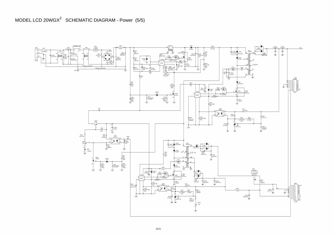
10-5
MODEL LCD 20WGX2 SCHEMATIC DIAGRAM - Power (5/5)
GND
G801
12V
ON-OFF
GND
5.1V
MUTE
5.1V
GNDGND
BRI
P-S
GNDGND
24V24V24V
GND
ON-OFF
TO INV
GND
BRI
5.1V
GND
2.0
2.5
12V
CUT
CUTCUT
CUT
12V
VCC
+24V
R8061M
1/4WMGF
R8211M
RM1206
+C843
100U/25V
R866
470 0805R80910.7K-MF08051/8W
L801
280uH
R883200K-F08051/10W
C8540.01U/1KV
Q804
2N70021
23
R855
20K08051/8W
D817FCQ20A06
23
1
T803RING CHOHE
13
24
+C857
1000U/16V
R843
1K 0805
P801
CON3
1
3
2
L
G
N
T806ER2834
3 12
1
6
5
8
10
7,11
9
2
Q881BT1691
3
2
C8551uF/450VMEF/P15
C847
0.01U 0805X7R
P803
12345678910111213
R83530.1K 1%
0805 1/10W
R86120K
D861
ER104
21
C8521000P 0805NPO
C8060.47U/275V
R812
15 MOF
R8342M
1/4WMGF
L803
5.4UH
R826200K-MF
08051/10W
D812P6KE180A
R85310K
RM 0805
P802
123456789
+C845
1000U/16V
R8671M
RM1206
C8131000P 0805NPO
D815ER1002FCT
23
1
R8130.39/2W
C8641000P 0805X7R+
C81210uF/50V
12
I813LTV817
1
23
4
R8191K 0805
R814
22 MOF
R84533K 1%RM0805
C818
1uF 080516V X7R-K
C8281000P500V X7R
C8620.1 0805X7R
5
4
38
7
621
I808
SG6841
C8810.47U/50VK
X7R 1206
C819
0.01U 0805X7R
5
4
38
7
621
I801
SG6841 R815200 MOF
R81756K 0805
+C835
1uF/50V
12
D806
1N4148
21
R8400.39/2W
R825649K-F08051/10W
C836 1000P/250V
R8242M
1/4WMGF
R862
47
+C801
150U/450V
+C820
4.7U/50V
ZD80422B
I802LTV817
1
23
4
R8021M
1/4WMGF
C8304700P 1KV
X7R
Q803FQPF13N50C
1
23
ZD88127C
R85233
R8812M
1/4WMGF
R857
22 MOF
F801
3.15AH250V
R8421K 0805
R805100 MOF
+C846
1000U/16V
+
C811470U/35V
D816
1N4148
21
D801
P6KE180AC802
1000P/250V
D807
ER306
ZD80327C
R84810KRM0805
ZD80230D
C8171000P 0805X7R
ER2819
5
164
10
R80829.4K 1%RM0805
D808
1N4148
21
D814PG108R
R82218K 0805
8
3
54
7
126
I809
L6562
L806
BEAD/6mm
R846 26.1K 1%RM0805
I807LTV817
1
23
4
+
C814470U/35V
Q808A733
3
1
2
I806AP431 1%1
A
2C
3R
C8030.47U/275V
+C861
10uF/50V
12
R81856.2K 1%
C8491000P100V X7R
VR801
10K
Q805C945
3
1
2
C851220P 0805X7R
D804PG108R
D881
1N4148
21
Q802
FQPF8N80C
12
3
C8310.47U/50VK
X7R 1206
R8100.27/2W
D805ER1004FCT
23
1
R82710K 1/2W
C850100P
1KV X7R
R839200 MOF
R854100KRM0805
C810100P
1KV X7R
+C848
4.7U/50V
R841270 0805
T802ET-24
13
24
C8040.01U/1KV
A3963WV2-A3P
1 2
L810
4.7uH
R882127K-F08051/10W
C8081000P/250V
ZD80124B
R807
3.3
I804KA78R12
1 2 3 4
1 2 3 4
C8561uF/450VMEF/P15
R81116K 1%
08051/8W
Q801
FQPF8N80C1
23
+C807
10uF/50V
12
R856
100K
R838100 MOF
C8164700P 1KVX7R
R851 47 MOF
R801SCK105
C8291000P
500V X7R
R8236.49K 1%RM0805
- +
D802GBU4K
2
4
3
1
L804BEAD/6mm
R8161.2K 0805
R820
1K 0805
D813
ER104
21
C8324700P 1KV
X7R
R868
0.22 1W
+C853
10uF/50V
12
C8230.22uF 080516V X7R
L802BEAD/6mm
+C842
1000U/25V
R833470
T801ER2834
3 12
1
6
5
8
7,10
11
9
2
C805 1000P/250V
I803AP431 1%1
A
2C
3R
C809220P 0805X7R
C822470P
1KV X7R
11- 1
PACKING SPECIFICATION
TABLE OF CONTENTS
PageB Version ......................................................................................................................................... 11-2

11- 2
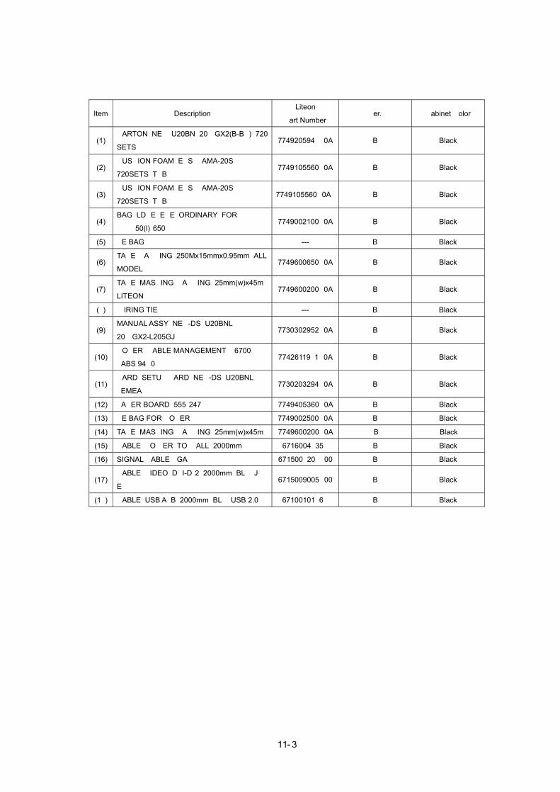
11- 3
Item Description Liteon
Part Number Ver. Cabinet Color
(1) CARTON_NEC_U20BN_20WGX2(B-BK)_720
SETS 7749205948P0A B Black
(2) CUSHION FOAM_EPS_KAMA-20SV_
720SETS_T&B 7749105560P0A B Black
(3) CUSHION FOAM_EPS_KAMA-20SV_
720SETS_T&B 7749105560P0A B Black
(4) BAG_LDPE+EPE_ORDINARY_FOR
HP_850(l)*650 7749002100P0A B Black
(5) PE BAG --- B Black
(6) TAPE_PACKING_250Mx15mmx0.95mm_ALL
MODEL 7749600650P0A B Black
(7) TAPE_MASKING_PACKING_25mm(w)x45m_
LITEON 7749600200P0A B Black
(8) WIRING TIE --- B Black
(9) MANUAL ASSY_NEC-DS_U20BNL_
20WGX2-L205GJ 7730302952P0A B Black
(10) COVER_CABLE MANAGEMENT_#6700_PC
+ABS 94V0 7742611981P0A B Black
(11) CARD_SETUP CARD_NEC-DS_U20BNL
_EMEA 7730203294P0A B Black
(12) PAPER BOARD_555*247 7749405360P0A B Black (13) PE BAG FOR COVER 7749002500P0A B Black (14) TAPE_MASKING_PACKING_25mm(w)x45m 7749600200P0A B Black (15) CABLE_POWER_TO WALL_2000mm 6716004835P B Black (16) SIGNAL CABLE VGA 6715008208P00 B Black
(17) CABLE_VIDEO_DVI-D*2_2000mm_BLK_JC
E 6715009005P00 B Black
(18) CABLE_USB A+B_2000mm_BLK_USB 2.0 6710010186P B Black

12-1
Revision History
Revision Revision
New Issue (1st Edition)
2006/03