SERVICE MANUAL CHASSIS CTR-AA - Electronica PT · eht 3671 mute v_vari 3612 a8 10u 2101 res 3005...
30
SERVICE MANUAL CHASSIS CTR-AA
Transcript of SERVICE MANUAL CHASSIS CTR-AA - Electronica PT · eht 3671 mute v_vari 3612 a8 10u 2101 res 3005...

SERVICE MANUAL
CHASSIS CTR-AA

CONTENTS Page
1.- Technical specifications 3
2.- Connection facilities 3
3.- Mechanical instructions 4
4.- Oscillograms 5
5.- Print board layout 6
6.- Electric scheme 7 - 12
7.- Circuit description 13
7.1.- Small signal processing, Microcontroller/Teletext 13
7.2.- RGB amplifiers 17
7.3.- Deflection 17
7.4.- Sound amplifier 17
7.5.- Power supply 18
7.6.- Protections 19
7.7.- Sets with SECAM L/L systems 19
7.8.- Stereo sets 20
8.- Electrical adjustments 22
8.1.- Service mode 22
8.2.- Power supply and focusing 22
8.3.- AGC adjustment 22
8.4.- White D 23
8.5.- Geometry 23
8.6.- Options 23
8.7.- Entering and exiting Plug & Play 25
8.8.- Error messages 25
9.- Safety instructions 26
10.- Service components 27
2

1 - Audio R 2 - Audio R3 - Audio L 4 - Audio5 - Blue6 - Audio L7 - Azul8 - CVBS status 1 9 - Green
10 - -11 - Green12 - -13 - Red14 - -15 - Red16 - RGB status17 - CVBS18 - CVBS19 - CVBS20 - CVBS21 - Earthscreen.
1. Technical specifications
CHASSIS CTR - AA
Mains voltage : 220 - 240 V ± 10% AC; 50 Hz (±5%)Power cons. at 220V~ : 35 W (14’’), 50W (20’’/21’’), 55 W (21" Real Flat), 3W (Stand-By)Aerial input inpedance : 75 � - coaxMin. aerial input VHF : 30µVMin. aerial input UHF : 40µVMax. aerial input VHF/UHF : 180mVPull-in range colour sync. : ± 300HzPull-in range horizontal sync. : ± 600 HzPull-in range vertical sync. : ± 5 HzPicture tube range : 14'' / 21‘’ / 21" RF / 21" PRF
: Mono: 25� 1W (14’’), 16� 2W (20’’/21’’): Estereo : 2x16� 2x4W (21’’), 2x5 W (21" Real Flat)
TV Systems : PAL BG: PAL I: PAL / SECAM BG / DK: PAL / SECAM BG / L / L'
Indications : On screen display (OSD) green and menu: 1 LED (red in On and blinking red in stand-by
VCR programs : 99, 0/ (new mask software)
Tuning and operating system : VST
UV1315A / IEC (VST) : VHFa: 48 - 168 MHz: VHFb: 175 - 447 MHz: UHF: 455 - 855 MHz
U1343A / IEC (VST) : UHF: 455 - 855 MHz
Local operating functions : Vol/Prog, +, -, contrast, colour, brightness and sharpness (and hue on program AV with NTSC signal).
3
Head phone: 8 to 600�. Mono : 25mW @ 32�
������������ ���������Stereo : 2x6mW @ 32�3,5mm ø.
2. Connection facilitiesEuroconnector 1
1 - Audio R 2 - Audio R3 - Audio L 4 - Audio5 - -6 - Audio L7 - -8 - CVBS status 2 9 - -
10 - -11 - -12 - -13 - Chroma14 - -15 - Chroma16 - -17 - CVBS18 - CVBS19 - CVBS20 - CVBS /Y21 - Earthscreen.
Euroconnector 2
(0V5 RMS@ 1K ) (0V5 RMS@ 1K ) ( 0V5 RMS @ 1K ).
(0V2 - 2V RMS @ 10K ).(0V7pp @ 75� ����
(0-2V int., 10-12V ext.).
(0-2V int., 10-12V ext.).
(0V7pp @75� ��
(0-V4 int.) (1-3V ext.@ 75� ��
( 1Vpp @ 75� �
( 1Vpp @ 75� �
Ext 1 Ext 2

3. Mechanical instructions
For the main carrier two service positions are possible (3.1).
A: For faulfinding on the component side of the main carrier.B: For (de) soldering activities on the copper side of the main carrier.
Position A can be reached by first removing the mains cord from it’s fixation, then loosen the carrier lips (1) and then pulling the carrier panel (2) for approximately 10 cm.
Position B can be reached from position A after disconnecting the degaussing cable. Put the carrier on the line transformer side.
A
B
Fig. 3.1
Fig. 3.2
4

5
4. Oscillograms


C14
A9
A6
A9
B8
C7
C5
C4
D3
+55
9371
TP16
A5
1%
1%
9061
9102
TP17
9014
C24
C26
C27
B29
B30
B33
B34
A1
A10
B13
A12
A6
A10
D11
A6
B2
A1
A6
+8F
+8F *
3000
9103
9416
9672
SDA_
2
A4
BG/L
B15
E36 D3
9013
9402
9401
9865
9682
+8
*33P
2604
*33P
2603
+3V3
9290
+8C
C23
C25
A12
D28
B32
B31
9010
9664
9608
23092U2
9094
9092GND GND
VHFIII
UHF
+8F
-TUNER -
3413
VGUARD
VHFIII
VHFI
LED
INTEX2
VHFIII
INT/EXT1
STBY
KEYBOARD
A2
1K53601
1K53602
+8
+5A
*6413
2418RES3416
+8
+8
22N2006 2017
+5A
+5
9435
2417100N
9669
9670
201810N
+5A
TP21
*23671N
*2304220N
+8
+89016
+3V3A
TP33
TP9
9403 9404
TP10
TP22
3031180R
+8C
*2299RES
*1K
3292
2613100N
+3V3A
+3V3
EHT3028
9004
CVBS_EXT
CHROMA
FB_EXT
R_EXT
B_EXT
BCL
CUT_OFFM7:5
M7:3R_OUT
G_OUT
GND_RGBM7:4
GND
+3V3+3V3
9093
9095
SC_AUDIO_OUT
V_VARI
9091
VHFI
2K3004
30062K
*3026
AM_IF
M10:2
- FRAME -
3414
RES
M10:19417
TP15
2403
47N
UHF
EHT
3671
MUTE
V_VARI3612
A810U
2101
3005
RES
*2003RES100U
2001
*34122K
*34112K
3415 9414
+55
9496
*361447K
361347K
3615RES
A3
*15K
3610
10K
3611
*24
K36
03
220N2610
2602
10U6602
E39
+8
9118
6020
*20
02R
ES
9434
9305
9671
9665
*PMBT23697605
9609
*3606
10K
B38
L/L'
SCL_
2
B37 C35
21041N2
2103
27K3018
2K2
3017
180R3019
*2102
*47R3015
334139K 1%
23074N7
23061U
10M
3305
100U2303 *2302
22N
*23052N2
22K
3656
TP34
9866
9674A1
9497
*202347N
*
22K3025
3371
*3372
*7004BC857
*
100N2031
*
1K3022
*2021
100N390R
3023 +8C
+8A
2034
47N
2036100U
3030
1R
*2298100N
*LL41486496
100R3295
100R3294
10U
5602
*2612100N
2601100U
36291K
12MHz1679
2622100N 100U
2623
9656
*36842K2
*2628100N
+3V3
*
2K23685
470R
3373
*63728V2
7005BC857
*3033
1K
1032
1033
*100R3034
+8C
TP32
1K3496
VGUARD
B_OUTM7:1
M7:2
+3V3
2600RES
+3V3+3V3
+8
100U2032
+8A503310U
+8C
9613
30022K
*3007
100R3003
3402390R
2005
470N
*2092RES
*
5K63008
+15
9011
AM_M
ON
O
9FBACK
7OUT_A
8GUARD
6VFB
5GND
4OUT_B
2Vi_B
3Vcc
1Vi_A
7401
9618
3K93101
2111330P
100N2340
*301447R
*23661N
15K3301
10U5301
9763
3618
1K5
3027100K
100R3293
560110U
RES3621
9536
3
1
2 5
4
1015
+8
60905V1
TP11
+8
+3V3A
*2609
3680
SWB
- TV PROCESSOR -
D16LINE_DRV
H_FLYBACK
D11
SIF E19
INT_CVBS
C21
TP30
TP29
GND
*3102820R
A7
31031K2
*2106
*2091RES
*3K3
3029
*30373K3
3020
47N2007 - IF -
50101U2
*24122N2
2N22411 *2308
22N
3406100R
2416100N
*BC8477601
*2301220N
9140
2611220N
*3604150
*3605220K
*2608
*360722K
+3V3A
- MICROCONTROLER - - TXT -
STBY
+3V3A
*368222K
SC_AUDIO_IN2105
D17
C18
330R3032
8U25032
- VIDEO -
3035100R
C20
C22
AUDIO_OUT
*100N2291
*100N2292
G_EXT
*2290 470P
*349510K
TP28
3628100R
RC5
10U5607
24C047685
*7104BC847
*3K33104
5012JMP
RES
*2K7
3410
3407
100R
2010
100N
*100R3291
*100N2293
32NC
31SNDPLL/SIFAGC
28AUDEEM/SIFIN1
27TUNERAGC
26VSC
25IREF
24IFIN2
23IFIN1
22VDRA
21VDRB
20AVL/EWD
19DECBG
18GND3
17PH1LF
16PH2LF
15DECDIG
14VP2
13SECPLL
12VSSA
11P0.6
10P0.5
9VSSC/P
8P3.3/ADC3
7P3.2/ADC2
6P3.1/ADC1
5P3.1/ADC1
4P2.0/TPMW
3P1.7/SDA
2P1.6/SCL
1P1.3/T1
56VDDC
57OSCGND
58XTAL_IN
59XTAL_OUT
60RESET
61VDDP
62P1.0/INT1
63P1.1/T0
64P1.2/NT0
55VPE
54VDDA
53BO
52GO
51RO
50CUT_OFF
49BCL/VGUARD
48B2/UIN
47G2/YIN
46R2/VIN
45INSSW2
44AUDOUT/AMOUT
43NC
42CVBS/Y
41GND1
40CVBSINT
39VP1
38IFVO/SVO
37PLLIF
36EHT
35AUDEXT/QSSO/AMOUT
34FBISO
33HOUT
30GND2
29DECSDEM/SIFIN2
7015

A8
E45
A37
A13
A33
A31
L2:5
L2:3
FF FF
+200
D42
D43
A34
B45
A29
A30
A32
L2:4
L2:2
14" 9686
9684
AQU
A
*3197
+8
+200
9167
9166
9168
25KV
FOC
US
2112
2U2
L2:1
3125
+8B
TP36
9123
+8
+8B
D39
D40
*3199 *3198
D41
L1:1
2208
- DISPLAY -
HPH_R/SPKSWE46
HPH_LE47
HPH_MONO C48
HEADPH_GNDE49
A2
A15
B45
BG/LA38
D44
0R053670
2636100U
B6
B3
1K3635
B4_45346636
+3V3
+3V3
B4
*22K3122
*
10K3116
*
BC847
7103
*
BA6826101
*10N2107
*31186K8
+3V3
2685100U
20"/21"
36611K
*
220N2126
21094U7
4U72108
+200
GND
+3V3
3229
1K5
3203
1K5
9169
219210N
+3V3
31191R
*2125100N
5235
1M1
33 L6
*3196
B5 -MONO-319168R2194100U
47K3127
1K3126
*7102BC847
- AM MONO -
VG2
6230
22372N2 TP20
51R
3205
FOCUS
C46
KEYBOARD
AM_MONO
AM_AUDIO_OUT
*3662
*3636
100R
*36751K3
270R3666
*3114
2K2+8B
*31172K2 RES
2202100N
1K53216
36273K3
L1:4
L1:3
1K5
3226
*7106BC847
32361K5
1M1
L3
LED
AM_AUDIO_OUT
L/L'9122
AM_IF
B1
CUT_OFF
R_OUT
*3221
3220
B_OUT
B4_45346663
9619
*36691K
*BC8477607
+3V3
RC5
36263K3
RGB_GND
G_OUT
3217
560R3207
9687 2196
9685
GND
+3V3
B2
4U72124
470P2204
3206
9226
*3665680R
*
1K33667
+3V3
3214
A-D
3664
100R
23
11685
TSOP1836SS3V
1
3
11
10
2
42
4
5
3
2
1 1101K9650M
1 IF_IN
2 NC
3 CAGC
4 CREF
5 NC
6 AM_OUT
7 AM_IN
8 AF_OUT 9EXT_IN
10SW
11+12V
12MUTE
13GND
14+8V
15NC
16IF_IN
7125TDA9830
7
8
9
2
1
3
6
4
5
7200
TDA6107JF/N3
- AM SOUND -
- RGB & DISPLAY COMPONENTS -
24P+
25P-
23
1
TSOP1836SS3V
1636
26MENU
R
B
FF*
FF
VG1
VG2
AQUA
G
FF*
B
FF
R
G
VG1
VG2
23

A23
C66
E46
C52
A20
C52
+8
+8
E59
A5
E63
+8
A14
E67
+5B
A4
B47
B46
C53
C54
E51
E50
A22
C55
9113
9143
2714
A18
A21
A24
C53
C52
AV_C
VBS_
IN
AV_A
UD
IO_I
N_L
+8
9809
*2828100N C9
+
-
55
SC1_
AUD
IO_O
UT_
R
INA+
SC2_CVBS
+8
+13B9181
+13B
9170
C5
C4
+13B
+13B
3190
+8
+8
*
330P2864
2189
C69
OUT+_MONO
OUT-_MONO
TP35
C53
A35
A21
C55
C8
SWA
E60
E57
FB_EXT
C54
*2191
C72
OUT+_MONOC71
C73
C69
E62
VIDEO
9296
AUDIO
GND
E64 E65
GND
GND
GND
A25
MUTE
C710U2147
C1
*3184
*
22K3140
*22K3141
*LL41486147
*314210K
+13B +13B
*6865LL4148
*3889220K
+8382547K
*2801100N
*
330P2863
1K3840
*
100R
3846
3836470R
220N
2185
*
220N
2181
317110K
*
10K3145
3194RES
9145
*2839RES
2837100N
+8120R
3837
2179220N
+13A
+ -48
7822BC847
10K3821
382210K
22K3820
3829
10K
7831BC847
2865330P
+8382310K
*2832100N
*
10K3867
*3863
8K2
*
LL4148
6851
INA+
IN-
INB+
MODE
+13B
C70
IN-
E56
E58
A7
C2
OUT-_MONO
9144
9151
C68
MAIN_L
INB+
IN-
C70 MODE
C66
3175RES
*3170INA+
RES
*3830100R *
3834 75R
*38
56
9802
*2859
*38
54
*3810
*389610K
*3852
2852*2856
+8
*
BC8477876
38805K6
386575R
286718P
2825
315582R
*2184
220N
*2193
220N
GND9191
+13B100N2154
AV_A
UD
IO_I
N_R
*38038K22804330P
3805
GND
*
75R
3851
*
75R
3853
A - E - F
9196GND_AUDIO
GND
GND
8K23801
C3*
3888
220K
*
330P
2854
*
150R3860
100R
3841
100R
3843
*
470R3876
BC8477875
3874
A27
A26
A20
*3890220K
382622K
BC8477878
1K53838
1VCC
2OUT+
3IN+
4MODE
8GND
5IN-
6SVR
7OUT-
TDA8941P7187
3189
1R
7830BC847
24k2%
388538
69 10K
*3868
8K2
10K3832
*3892
100R
*387075R
218210U
3714
+13B
3898
*
2850
3850
*
100R3872
2155100N
315482R
+
-
54
*38
08*
75R
3855
SC1_
AUD
IO_O
UT_
L
*
220K
3873*2860
100R3814
100R
3845
SC_A
UD
IO_O
UT
HPH_MONO3193
HPH_R/SPKSW
SC1_CVBS_IN
SC2_CVBS_IN
SC1_CVBS_IN
SC2_AUDIO_OUT_L
- SECOND SCART-
CHROMA
21951N5
2187
3186
*2188
C72
CVBS_EXT
9291GND
SC2_AUDIO_IN_R
SC1_AUDIO_IN_L
SC2_AUDIO_IN_L
AV_CVBS_IN
CVBS_EXTSC2_CVBS_IN
- SCART + AV -
+13B
*2190220N
GND
GND
GND
B_EXT
R_EXT
AUDIO_OUT
MAIN_R
*3183
*
100K3147
*7140BC847
- AMPLIFIER -
INT_CVBS
AV_CVBS_IN
SC2_AUDIO_OUT_R
*
330P2855
*
150R
3861
*3835100R
1N52198
C68
C69
C66
*3185RES
+ -
66
C71
C6
3831RES
SWB
SC2_CVBS *100N
2833
*
18P2834 *38
0410
K
SC1_AUDIO_IN_R
SC_AUDIO_INGND
2853
RES
*
2851 RES
INT/EXT1
INTEX2
*
10K3886
SC1_CVBS_IN*6849
LL41489891
GND_AUDIO
1N52183
GND
GND
GND
*
10K
3802
2802330P
*3864150R
G_EXT
*
68R
3875 INT_CVBS
286618P
3877120R
2876100N
*BC8477141
*3866150R
*
75R3871
*68R
3839
RES
3883
*3879
*385875R
7NC
5NC
3VCC1
1OUT1-
6IN1+
4OUT1+
2GND1
15GND2
13NC
11SVR
9IN2-
16VCC2
12IN2+
10MODE
8IN1-
17
OUT2-14
OUT2+
4
3
2
1
9
8
7
6
5
TDA8943SF7187B
OUT-
VCC
OUT+
IN+
IN-
SVR
MODE
GND
NC
7187C
*3830
2834
*
75R
100R
18P
3834
*
*3803
3804
*
330P28048K2
10K
1215
13
876
1
4
11
10
14
2
5
3
16 9
VssVee/E
Vdd

+8E
4 3
FF FF
9504
TP8
A3
RES
50:1
D1
A16
A17
TP12
+200
M6:
4
M6:
3
6540
6541
TP199667
9464
A11
A28
B43
B42
B44
50:2 1500T 2.5 A H
2556
+3V3
LINE_DRV
+55 34463447
TP3
5 12
9508
*
LL41486440
3N32524
B41 B40
2442560P
9506
TP5
2505
B39
10U2470
FERRITE5532
357047R
+13
5534FERRITE
*
RES6571
3572
+8
+15
TP40
STBY
+13C
TP7
+3V3
TP6
+5
TP39
+15
470U2467
350410M
95103558 *6558
*BC8477556
+VCC_LINE
H_FLYBACK
- LINE -
2500470N
1
2
4
6
7550 3550
100R
544022U
2440
1U
3444
RES
64461N4148
9507
*2528RES
*6521RES
251447U
9509
344110K
150R3448
2450
3456
*252747N
6511
1N4148
3522
1K2
TP2
FERRITE5533
25101N
6502
1N40
0765
03
1N40
07
1N40
07
6504
6505
1N40
07M
6:1
34425K6
3480
6451BYT42M
TP13
+VCC_LINE
TP4
65241N4148
251547U
3525
10R
6523BAV21
3238
34704R7
3235
2445 6447
TP14
3457
10N2449 2448
3519TP18
3540RES
1K3542
*
39K35362539
22N
+13
3539
470R3571
*65703V3 2%
RES
2534
6530
BYW36
1R3449
544910U
3452
6531
1N4148
9572
3531353322K
2540
1540
2455470U
6449
245322U
12K
3462
353722K
+13
+13A
22U2561
*
C5V6 2%6479
*3477100R
9479
4U72462
EHT
BCL
25KV
VG2
FOCUS
3557 100K3555
+13C
PTC
3501
*
47R3445
1
2 3
430882
5441
54809480
3N3
2506
7445
M10:3
3535
1K
9575 3541
3576130R
2533
7575BC337
+13
2454470U
6450
BYT42M
7479BC337
TP1
9598RES 9502 49:2
49:1
+3V3
3455
9542
470P2532
+VCC_LINE
+VCC_LINE_A
+8E
+55
+8D
- POWER SUPPLY -
*3511
3526470R
BAV216525
270K 0.5W3528
1
2
1
2
222
4 3
1
5500
2502
2N2
2504
2N2
270K 0.5W3527
3556
9550
7555
DEGAUSS
100R
34407440
BF422
33K3451
10U2451
A,B
KA431LZ7533
*7572BC847
47K3534
2531RES
5538
0R053573
POR
100N
2562
47U2530
3530
470R
3475
BYT42M
64706452
BYT42M
+8+8D
2446
3460
246047N
LL4148
6463
10N
2458
544747U
9599RES
VCC
FBSYN
C
GN
D
DR
AIN
7514KA5Q0565RT
244447N
*3532RES
10
7
9
3
5
1
8
12
4
2
5525
*7571BC847
+VCC_LINE_A
3450
1R 1/2W7478RES
M10:6
9
10
6
3
7
5
4
8
1
2
11
5445
7515TCET1103G

E2
C59
C60
C57
C58
C65
C51
C50
C73
9722
9762 9761
9721
+5C
2799
100U
E74
C64
B49
B46
B47
C67
E74
C63
B45
C56
A33
A39
A36
GND9710
GND
GNDGND
GNDGND
GNDGND9712
9727
9714
*2783 3762
- MULTI -
+5B
TP31
TP27
+5B
*2758470N
*
470P2761
276547U
2772470N
E4
- 2ND SCART-
TP25
TP41
C62
A19
*3710
+5B9148
*27P2740
*37416K8
E1
100R37509728
- STEREO -
*2782 3763
*2720RES
24.576MHz1750
2785RES
5753
FERRITE
TP24
*120P2742
RES3742
470N2750
+5B
37483K3
*
2791RES
*
2790RES
3756270R
*2763470P
276047U
276610N
276810N
10N2767
277010N
277310N
277510N
2777470N
2789RES
*2757
*
2788RES
*2780
330N
*
330R
3703
3704
RES
RES2703
*27622U2
2774470P
2778
2U22776470P
+8E
*377433K 7780
BC547
37693K3
+13B+8E
BC547
7781
*37713K3
TP26
+5B
9703
270247U
5702JMP
9704
RES
9781
9780
*37810R05 2798
100U
100R3751
2K2
3760 *2755
470N
*3K33749
10K3752
275947U
*2781
330N
*2756
330N
2779
2U2
*27642U2
3702RES
+13B33K
3772
AV_AUDIO_IN_L
AV_AUDIO_IN_R
GND
AM_AUDIO_OUT
GND_AUDIO
SWA
2787RES
SDA_2
SCL_2
SC1_AUDIO_IN_L
SC1_AUDIO_IN_R
MONO_AV
SC2_AUDIO_IN_R
SC2_AUDIO_IN_L
- 2ND SCART-
+5B
SC1_AUDIO_OUT_L
SC2_AUDIO_OUT_R
SC2_AUDIO_OUT_L
E3
HEADPH_GND
HPH_R/SPKSW
*37800R05
HPH_L
MAIN_R
MAIN_L
MONO_AV
+3V3
3764
2753470N
*37531R
*27541U
574122U
SIF
*
100N2751
L/L'
- MULTI -
A - C
15K3755
15K3761
*
C5V6 2%6702
BC3377702
+5C
+8E
3705
100R 1/2W
SC1_AUDIO_OUT_R
*3773330R 1/4W
*2771
4U7
2R23770
FERRITE5757
*2741180P
3758
15K
3754
15K
3706100R
*3775330R 1/4W*2769
4U7
32EXTIL
31EXTIR
30TEST2
29MONOIN
28TEST1
27SDI1
26SDI2
25SDO1
24SDO2
23WS
22SCK
21SYSCLK
20P2
19XTALO
18XTALI
17Vssd4
16CRESET
15Vddd1
14Vssd1
13ADDR2
12SIF1
11Vref1
10SIF2
9P1
8Iref
7Vdec1
6Vssa1
5SDA
4SCL
3ADDR1
2NICAM
1PCLK
56Vssa3
57AUXOR
58AUXOL
59Vdda
60MOR
61MOL
62LOL
63LOR
64Vddd2
55PCAPL
54PCAPR
53Vref3
52SCOL2
51SCOR2
50Vssa4
49Vssd2
48SCOL1
47SCOR1
46Vref2
45i.c.
44i.c.
43Vssa2
42i.c.
41i.c.
40Vref(n)
39Vref(p)
38Vdec2
37SCIL2
36SCIR2
35Vssd3
34
SCIL133
SCIR1
7701
---
A6
A7
A2
A5
---
HZT33
100R
10K
100R
YES
---
YES
YES
VST
BY448
BAV21
84UH
360K
560R
---
270K
---
JMP
JMP
---
YES
---
---
9809
9802
9450
9449
9151
9144
9143
9113
9004
6541
7187
6540
6449
5525
3854
3850
3808
3572
3511
3196
3193
3190
3184
2860
3183
2859
2856
2852
2850
2540
2533
2196
2189
2187
2188
2105
2106
2103
2102
1540
48
C7
C5
C3
A8
JMP
---
---
JMP
---
---
8K2
3K3
5K6
4N7
---
---
2U2
3N3
YES
---
---
---
YES
JMP
---
JMP
JMP
---
---
8K2
3K9
5K6
4N7
---
2U2
3N3
YES
---
YES
---
YES
---
JMP
---
---
JMP
47K
---
6K8
---
JMP
---
---
---
---
33P
---
YES
---
YES
---
9609
6020
3020
2608
2017
1032
E2
B2
3415
2450
2445
---
---
---
47U
5.5
---
---
BG
5R6
---
14"
JMP
---
---
47K
YES
---
---
---
0R05
---
47U
6.0
---
---
I
3R3
470N
220P
21"
---
1K
---
---
---
---
47U
5.5
---
---
3R6
---
21"
---
YES
3R3
LG21"
I
---
---
---
47U
5.5
---
---
2V4
12K
---
100U
5.5
YES
---
---
---
15K
3K
2U2
330N
18P
YES
YES
---
3R6
220N
1N
---
---
---
220K
37551
13V
5K1
---
560R
1M
YES
3810
3852
3856
5538
C4
C6
E
B5
JMPJMP
---
---
JMP
---
8K2
JMP
---
---
---
---
---
10U
---
YES
---
---
YES
1W
MONO
---
JMPJMP
JMP
JMP
JMP
8K2
---
---
---
---
---
---
10U
---
---
YES
---
---
---
2W
JMP
------
---
---
---
47K
---
---
10N
---
---
22N
---
---
YES
YES
YES
TXT
9608
7015
3125
1033
2609
2191
E1
1015
B1
3238
2446
---
---
---
JMP
---
PAL
---
---
---
8N2
---
---
---
---
JMP
---
PAL
---
J1952
8N2
1R
+104.5
---
6.5
---
---
JMP
---
---
8N2
1R
---
YES
8N2
---
---
---
6.5
JMP
---
---
JMP
---
JMP
6.0
K2962
YES
YES
15K
JMP
---
330N
---
330N
3K
---
YES
YES
YES
6N8
---
9575 22R 0.5W
7445 BUT11AF
RGP15M6447
6230 JMP
---5480
3541 22R 0.5W
3530 FERRITE
3480 ---
47R 1W3457
560R 1/2W3447
4R7 0.5W3416
270K3413
1R 0.33W3235
3220
560R3214
220K3028
2450
2446
1U 200V2208
B3 YES
14"
3680
6602
3026
3612
1001
3007
47R 0.5W
RGP15M
BAV21
DC-12
47R 1W47R 1W
4R7 3W4R7 3W
1K2 1W1K2 1W
10R 1W10R 1W
820R 1/2W
3R6 0.5W
360K
2R 0.5W2R 0.5W
560R
---
220K
10U 250V
---
20"/21" 21" RF
BZX79-C33
100R
UV1315AI
100R
CTF5560
PLL *
BYT42M BYT42M
100K 100K
0R05 0R05
0R05 0R05
220P 220P
680U 16V
10U 25V10U 25V
220N
220U 25V220U 25V
---
JMP
---
---
JMP
BYV98-200
BYW32
SOPS 4W+4W
47K
270R
---
6K8
---
JMP
330P
330P
---
100U 25V
---
1000U 25V
---
33P
---
YES
---
YES
---
NO TXT TDA9370PS/N2
0R05
9763
9140
3898
3879
C2
NICAM+A2
JMP9145
66
MONO
470N
TDA9381PS/N2
0R05
BG DK
MONO
JMP
24K
A2
---
YES
MONO
330N
THOMSON
TDA9370PS/N2
---
---
0R05
---
47U
5.5 5.5
---
---
BG
9714 ---
3805 ---
3762 ---
3671 100R
2825 0R05
2782 330N
2714 ---
C8 ---
B6 ---
A3 YES
1SCART
3R6
470N
220P
PHILIPS21"
TDA9381PS/N2
---
---
0R05 0R05
---
47U
6.0
------
--- ---
BG DK
STEREO
JMP JMP
0R05 0R05
0R05 0R05
100R 100R
0R05 0R05
330N 330N
18P ---
---YES
--- ---
YES YES
+ FRONT AV
3R63R6
270N330N
---
THOMSON21" 21" RF
BG L L'
2SCART + AV
21" RFPHILIPS
TDA8357J/N27401
9480 JMP
3531 180K
LOT 14"5445
350015500
6413 11V
33R 0.33W3452
3460 7K5 0.5W
560R 1/2W3446
3519 5K1
3415
3238
560R3217
3221
3206
2505 56U 400V
2448 10U 200V
2445
---B4
TDA8359J/N2
---
180K
37551
LOT 21" RF
13V
820R 1/2W
6K2 0.5W
1R 0.5W1R 0.5W
4K7
---
560R
1M
68U 385V
47U 200V
YES
BYT42M BYT42M
0R05 0R05
6K2* 6K2*
680U 16V
220P 220P
T 1A LT 630mA L
220N
JMP
------
---
---
---
TDA8944J
FERRITE
270R
47K
---
---
1R 0.5W
820R
0R05
10N
1500U 25V
---
330P
---
T 2.5A L
22N
---
---
YES
YES
YES
4W + 4W
STEREO
TDA9350PS/N2
G1961/G1975
TDA9875A/27701
OLDMICRO *
STEREO
+101.5
TDA9351PS/N2
PAL/SECAM
K2955
TDA9870A/2
NEWMICRO
2 SPEAKER
STEREO
+106
TDA9350PS/N2
---
6.0
JMP JMP
---
---
---
G1984
---
---
PAL
3762
9891
9296
JMP
---
15K
2783
3662
3714
2757
---
---
270R
---
C1
A4
A1
C9 ---
---
---
---
---
+104.5
9N1
---
TDA9351PS/N2
---
---
JMP
---
K2977J1981
--- ---
------
PAL PAL/SECAM
JMP JMP
JMP JMP
15K 15K
100R ---
0R05
0R05 0R05
270R
0R05
270R
YES---
---
---
---
---
---
---
1R1R
+107 +123.5
1SCART
7N58N2
PAL/SECAM
+121.5
47R 0.5W
BUT11APX-1200BUT11APX-1200
SOPS MONO SOPS MONO
820R 1/2W
3R6 0.5W
SEE CRT TABLE
SEE CRT TABLE
10U 250V
* SOFTWARE MASK /1513 /1515 /1516
TDA9370PS/N2 TDA9381PS/N2
YES
2V4
12K
10P
BYV28-200 100U
BYW32
SOPS 5W+5W
270R BG L L'
* SOFTWARE MASK /0763 /0776 /0946 /1052
330P
330P
1000U 25V
390N
470P
SAMSUNG
TDA9370PS/N2 TDA9381PS/N2
+LATERAL AV
SAMTEL
TDA8359J/N2
LOT 20/21" TDA8941/N1 TDA8943SF/N1
820R 1/2W
6K2 0.5W
SEE CRT TABLE
SEE CRT TABLE
56U 400V
47U 200V
SEE CRT TABLE
TDA9350PS/N2 TDA9351PS/N2
YES
TDA8946J
10P
10K
FERRITE
270R
PAL/SECAM
K2962
1R 0.5W
0R05
820R
1500U 25V
330P
T 2.5A L1 SPEAKER
VCC_LINE 104.5
5W + 5W
TDA9350PS/N2 TDA9351PS/N2
1SCART
*NOT PLACED IN SOFTWARE MASK /0763 AND /0776
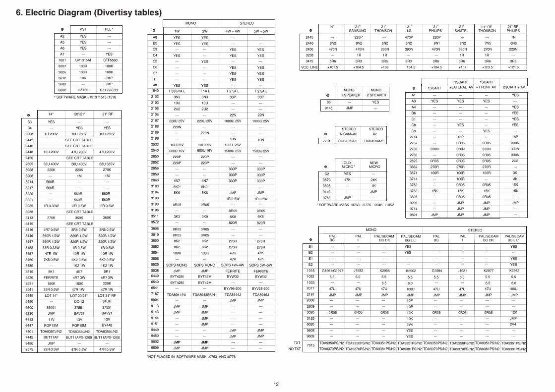
6. Electric Diagram (Divertisy tables)
12

7.- CIRCUIT DESCRIPTION
7.1.- SMALL SIGNAL & MICROCONTROLLER/TEXT (Diagram A)
The small signal is processed by IC 7015. This IC called Ultimate One Chip (UOC) also has an embedded microcontroller.
The CTR-AA chassis is designed to use 5 possible IC's in position 7015, 3 for PAL systems, (TDA9350 with teletext;
TDA9380 and TDA9370 without teletext) and 2 for multi-standard sets (TDA9351 with teletext; TDA9381 without
teletext). The associated circuitry is the same for TXT and non-TXT models.
In this chapter 7.1 TV sets with mono sound and PAL systems are explained. The associated circuitry for
sets with SECAM L/L' systems is explained in chapt. 7.7, whereas for stereo sets can be seen in chapt. 7.8.
The small signal part includes IF detection, video processing, chroma decoder, RGB, sync processor and sound decoder (mono sets). It is fully controlled by the embedded microcontroller.The microcontroller contains a specific program that assures all the functions of the appliance, including 2 menus, one to control the set (see Instructions Manual) and another for Service Mode (see Service Instruct. chapter 8).The IC for TXT sets (TDA935x) contains a teletext decoder, including the following functions: TXT on/off, reveal, freeze, temporary cancellation, clock, subcode, zoom, index, flof, page +/-, X/26 and 8/30 packet decoding (station identification and start-up page).
Fig. 7.1: TDA93XX block diagram
7.1.1.- IF detectionIF detection is intercarrier type, that means that sound and picture are detected in the same circuit (PIF).- IF amplifier (pins 23, 24): The IF signal coming from pin 11 of the tuner (1001) is filtered by the IF SAW filter (1015) and applied to IF amplifier of IC7015 by means of pin 23 and 24 input. The IF bandpass characteristic is determined by the SAW (Surface Acoustic Wave) filter.- PLL demodulator (pins 37, 58, 59): The IF-signal is demodulated by means of a PLL detector, which one is used to regenerate the IF reference signal. Reference signal is determined by the PLL loop-filter pin 37 and calibrated by microcontroller crystal (pins 58, 59). It is alignment free.Demodulation is achieved by multiplying reference signal with the incoming IF-signal.- AGC (pin 27): The IF AGC time constant is internally fixed. The tuner AGC voltage (pin 27) is applied to pin 1 of the tuner and adjusted by microcontroller (see chap. 8.3).- Video output (pin 38): This baseband CVBS signal with 2.5Vpp (sync inclusive) of nominal amplitude, contains the FM intercarrier sound signal. Sound is filtered out by a ceramic trap (1032 or 1033) which frequency can be different depending on the system: 5.5 MHz for BG, 6.0 MHz for I system and 6.5 MHz for DK system.
13 12
7.1.2.- Sound processor- FM demodulation (pins 31, 29): FM sound is filtered from CVBS (pin 38) by a loop-filter (pin 31) and demodulated. Decoupling sound demodulator is made by a capacitor on pin 29.- De-emphasis and audio out (pin 28): De-emphasis is made by C2102 at pin 28. The signal at this pin is driven to the euroconnector sound output (see Diagram C) by transistor 7104.- External audio input (pin 35). The External Audio signal from pins 2 and 6 of Euroconnector 1 (or from the Audio in the A/V connector, if the set has one) enters through this pin. The selection of external or internal audio is made through an internal switch, which is controlled by bus I²C (see INT/EXT, chapt. 7.1.8)- Audio out (pin 44): After a volume control (by I²C), this output is driven to the input IN+ of the final sound amplifier IC7187 (Diagram C).
7.1.3.- Video processing- Video switches (pins 40, 42): The internal CVBS signal proceeding of pin 38 is now fed to pin 40 of 7015. External CVBS proceeding from pin 20 of Euroconnector is present on pin 42 of 7015. The IC switches between internal and external are controlled by I²C bus (see INT/EXT, chapter 7.1.8).The selected CVBS signal is internally supplied to the synchronization, teletext acquisition circuits and the video identification circuit for IF ident.- Luminance processor: CVBS is also internally applied to luminance processor, which is composed of chrominance trap filter, luminance delay line and peaking circuits. Sharpness control modifies peaking by I²C.
7.1.4.- Chroma processingThis circuit is an internal (no pins associated) automatic decoder for Pal and NTSC systems commanded by I²C bus.- ACC and chroma filter: Video signal coming from video switches is supplied to PAL/NTSC chroma bandpass filter via a variable gain amplifier which is controlled by ACC and ACL detection circuits.The dynamic range of the ACC is 26dB and detects only the burst amplitude. The ACL is a chroma amplitude detector and is active when the chroma/burst ratio exceeds approximately 3. It ensures that CVBS signal to chroma bandpass filter is limited for large.- PLL/DCO: Chroma PLL is integrated and it operates during the burstkey period; the DCO (digital controlled oscillator) generates a subcarrier signal Fsc in phase-lock with the incoming burst signal. The reference signal for the DCO (Fref.) is derived from the crystal oscillator (1679). Different colour frequencies are internally switched by I²C. The hue control rotates the DCO reference phases (H0, H90) from -40 to 40 degrees for NTSC signal via I²C bus.- PAL/NTSC demodulation: The 0ª & 90ª signals are supplied to the burst demodulator circuits to obtain (B-Y) and (R-Y) respectively. Chroma delay lines used in demodulators are internal.
7.1.5.- RGB processor- External RGB inputs (pins 46, 47, 48): RGB inputs coming from euroconnector (see diagram C), are AC coupled (C2291/92/93) and converted internally in YUV signals. Then are switched with internal YUV (YUV SWITCH) by fast blanking.- Fast blanking external (pin 45): When fast blanking is high external RGB is displayed, only if TV is in external AV (program 0). Fast blanking can switch signals for full screen (by a DC voltage) or for a part of the screen (by a pulse voltage).- Matrix: After switching, YUV signals are converted to R-Y, G-Y and B-Y in the internal MATRIX circuit. Saturation control is received by I²C bus.- Black stretcher: Internally the luminance signal is connected to the YUV select circuit and via the input clamps it is supplied to the black stretcher. The black stretcher circuit, fully integrated, extends the grey signal level. This extension is dependent upon the difference between actual black level and the darkest part of the incoming video.RGB adder: RGB signals are obtained in this circuit by adding R-Y, G-Y and B-Y proceeding from matrix and Y proceeding from black stretcher.- RGB OSD: RGB inputs for OSD and TXT are internally inserted to RGB signals. Fast blanking used is also internal.45).- Beam current limiter (pin 49): The beam current limiter circuit functions as an average beam current limiter (BCL) as well as peak white limiter (PWL). Both functions reduce the contrast and brightness of RGB signals.Contrast reduction begins when Vpin 49 < 3.1V and brightness reduction begins when Vpin 49 < 1.8V.BCL: Average beam current present at pin8 of 5445 (Diagram D) is feedback to pin 49. When beam current is high, voltage of C2462 is lower, D6462 conducts and Vpin 49 decreases.PWL: This circuit is an internal detection circuit, which comes into action if the difference between measurement DC level and white level exceeds approximately 2.6V. Then a current of 200µA is internally produced to discharge 2298 and Vpin 49 decreases.- RGB output circuit (pins 51, 52 and 53): RGB outputs are driven to RGB amplifier (Diagram B).- Continuous Cathode Calibration (CCC) (pin 50): This circuit is an auto-tuning loop which stabilizes the black level (offset) as well as the cathode drive level (gain) of each gun. Pulses in 3 consecutive lines R, G and B (pins 51, 52, 53) at the end of frame blanking are used on alternating fields, one field for black level, following for cathode drive
14

level.Cathode currents of 8mA for black level and 20mA for cathode drive level are stabilized. Cathode current is present at pin5 of IC7200 (Diagram B) and measured on pin 50 (Cut-OFF Info). RGB outputs are adapted to keep cathode currents measured, for example when VG2 voltage is adjusted, DC level of RGB outputs is automatically corrected.- Warm-up detection circuit (pin 50): At the start up a DC voltage of 2.5V is present in the RGB outputs (pins 51, 52, 53). As soon as beam current is detected on pin 50, RGB circuit starts in normal operation. If RGB circuit is damaged or grid 2 is low, the RGB circuit could not start (black picture) due to current is not detected.
7.1.6.- Horizontal synchro- Start up: The horizontal oscillator starts is commanded by microcontroller. During start up circuit provides a softer operating horizontal output with a higher frequency.- Hor. sync. separator: Fully integrated sync. separator with a low pass filter, slicing level at 50% of the synchronized pulse amplitude.- Horizontal Phi 1 detector (pin 17): This circuit locks the internal line frequency reference on the CVBS input signal. It is composed of a phase comparator and an internal VCO of 25MHz (1600*15625). The free running frequency is stabilized using the 12 MHz reference of the X-tal oscillator.Phi 1 detector filter is made by external components at pin 50. Phi 1 time constant is automatically controlled by software for broadcasting signals. For video signals (AV and program 99) constant is always fast to prevent top bending on the screen.- LBF (pin 34): Line Fly Back input, is obtained by the network R3456/C2408 (Diagram D) and R3371/R3372. - Sand Castle (pin 34): Sand Castle output obtained at this pin is used only internally. Levels of sandcastle pulse are 5.3V for burst detection, 3V for line blanking and 2V for frame blanking.- Horizontal Phi 2 detector (pin 16): The flyback position respect line blanking on TRC cathode is controlled by this circuit. Phi 2 detector filter is made by C2305 pin 16. Horiz. shift can be adjusted by I²C (see chapter 8). EHT compensation is made through R3305.- HOUT (pin 33): Horizontal output is an open collector which one drives the horizontal driver stage (T7440 diagram D).
7.1.7.- Vertical synchro and vertical drive- Vert. sync. separator: It is an internal integrator to separate frame sync. pulses from CVBS.- Vertical divider system: The divider system uses a counter that delivers the timing for the vertical ramp generator in the geometry processor. The clock is derived from the horizontal line oscillator. Mode used is automatic 50/60Hz identification with 50Hz priority.- Vertical sawtooth generator (pin 25, 26): A reference current of 100mA is realized at pin 25 by means of an internal reference voltage (3.9V) and resistor R3341. This 100mA reference current is used to derive a 16mA current to charge C2340 (pin 26) during vertical scan. The charge current can be adjusted with the I²C bus control, (VERT.SHIFT). The external capacitor is discharged during vertical retrace by the vertical divider system.- Vertical geometry processor: The saw tooth signal that is derived from the sawtooth generator can be controlled by I²C bus. Control adjustments are: S-CORRECT, VERT.SLOPE, VERT.AMP and VERT.SHIFT (See chapter 8).- Vert. output stage (pins 21, 22): The vertical geometry processor has a differential current output to drive a DC coupled frame deflection (7401).- EHT compensation (pin 36): A voltage inversely proportional of beam current, proceeding of pin 8 of line transformer (5545 diagram D) is applied to pin 36 to stabilize vertical amplitude from EHT variations.- Vertical guard input (pin 50): A vertical retrace pulse proceeding from pin 8 of IC7401, is added to cut-off voltage at pin 50 (this pin has 2 separated functions, cut-off function see chapter 7.1.5). If there is not pulse or its level is not correct (should be above 3.65V, 0.8msec.), the set goes to standby mode. (See chapter 7.6.1 Protections).
7.1.8.- Microcontroller/ TeletextCTR chassis can work with several different microcontroller versions. The numbers that appear at the end of the description of the IC 7015 indicate wich is the software mask version: TDA93xxPS/N2/MMMM.Versions /0586,/0763,/0776,/0946 and /1052 correspond with the same software used in the previous CTU chassis.New software versions, /1196 and /1227, have now been introduced which make it possible to control a chassis with double scart, adding some new features like format function 16:9, which is accessed through the remote control (and with automatic Scart switching), the Plug & Play start up menu and the External and Sleep-timer keys.
Following there is an explanation of the different functions of the microcontroller indicating pins number assigned:- Tuning: The different systems available depend on the models in question, these could be Voltage Synthesized Tuning (VST) or Phase-Locked-Loop tuning (PLL).* Voltage Synthesized Tuning (pins 4, 11 and pin 8 or 10): this system works by tuning to a station on the tuner through a linear variation of the tuning voltage (V-VARI) from 0V to 33V applied on pin 2 of the tuner. It is generated on pin 4 of the µC and converted to an adequate level for the tuner using T7605.
While searching, µC are always reading internally AFC (Automatic Frequency Control) and video identification
15

signals.When video signal is identified, µC stops searching and do a fine tuning to reach a right AFC value.- Band switching: There are two outputs for band switching pin 11 for VHFI and pin 8 (one scart chassis) or pin 10 (double scart chassis) for VHFIII. The µC controls the channel band in the tuner by a voltage of +5V at the correspondent output. UHF band is controlled by means of transistor 7601. If the set is in VHF, one of the pins VHFI or VHFIII are high and transistor conducts in such a way the UHF voltage is 0V. If the set is in UHF, pins 8 and 11 are low,transistor is cut and the set is in UHF.
* PLL Tuning (pins 11 and 8 or 10, depending on the chassis external connectors): The tuning and band switching are totally controlled through bus I²C, which is based between pins 8 (chassis 1 scart) or 10 (chassis double scart) and 11 of the µC, and pins 4 and 5 of the tuner (1001). Neither the varicap voltage nor the band switching is used. Pin 2 of the selector has an extra voltage of 33V, stabilised by the zener 6602- Control key (pin 5): Pin 5 is activated by a DC voltage. When control keys are not activated, a voltage of 3V3 is produced by R3618. If one control key is activated, this pin is connected to ground directly or by a resistor R3665, R3667 (Diagram B), decreasing its voltage.There are 3 voltage levels depending of the key used: 0V for MENU, 1V for P- and 1.9V for P+.- Mute output (pin 6): This pin is a 3 state output used to control the sound amplifier (see chapter 7.4). States are 0V, open and Vcc (3.3V). In a chassis with new software version it is also used to generate the Standby signal from the source.- INT/EXT1 input (pin 7): The set can switch to external (AV on the screen) by remote control (selecting program 0) or by rise edge at pin 8 of euroconnector (see diagram C). The IC switches internally video and audio to external. In both cases the user can switch to internal changing the channel.If the set includes function 16/9, it will switch to that function directly through INT/EXT (between 4,5 and 7V), although it can also be modified through the remote control.- INT/EXT2 input (pin 8 in a double scart chassis): the TV can switch to the second euroconnector input through the remote control handset (External key), or alternatively through pin 8 of euroconnector 2 (see diagram C). - LED (pin 10 in one scart TV sets or pin 8 in double scart TV set): The LED (D6636 or D6663 diagram B) lights up with a low current when the television set is ON and with a high current when the set is in Standby. While the set is receiving a remote control signal, the led is blinking.- Picture controls (brightness, contrast, colour, sharpness) are processed internally by I²C bus.- Sound controls: Sound controls are processed internally by I²C bus- Standby: When the set is switched to stand by, line stops (pin 33). In addition to this, pin 1 with old software masks, pin switch to low level to make Power Supply in burst mode (see stand by 7.5.4). In new software masks, this function is realized through mute control pin.- OSD outputs: The RGB and fast blanking signals used for On-Screen Display (OSD) and also for TXT are internally inserted to RGB outputs (pins 51, 52, 53).- Oscillator (pins 58, 59): A 12-MHz oscillator is determined by a 12-MHz crystal (1679) between pins 58 and 59.- P.O.R (pin 60): Power on reset (POR) is internal, activated when the set is switched on. If the µC shows abnormal behaviour it is advisable to reset it switching off/on the set. Reset can be done also by a short circuit between pins 60 and 61.- RC5 (pin 62): The commands transmitted by the remote control handset are received by infrared receiver (1685 diagram B) and passed to the microcontroller for decoding.- EEPROM (pins 63 and 64): The microcontroller is connected to non-volatile memory IC7685 (EEPROM) via bus I²C.The following information is stored in the memory:- Channel data including tuning voltage and band of all the channels.- Personal preferences (PP), menu mix and child lock on user menu.- All settings included on Service Menu.
7.1.9.- Supplies and decoupling- Small signal analog supply (pins 14, 39): The same +8V supply coming from line deflection is connected to pins 14 and 39 for small signal processing. A separated supply (C2036) feeds video and sound traps circuit.If +8V supply is not present at pin 39 or pin 14 during the first 4 seconds after switch ON the TV set, the microprocessor goes to Standby mode (See chapter 7.6 Protections).- Digital supply (pins 54, 15): A +3V3 supply is used for digital circuit of TV processor (pin 54). A decoupling capacitor for this supply is present at pin 15 (C2301). Pin 54 is used also to supply the µC.- Bandgap decoupling (pin 19): The bandgap circuit provides a very stable and temperature independent reference voltage of 4.0 V which one is used specially in the analogue video processor part.- µC supplies (pins 54, 56, 61): The µC has several +3V3 supplies,?Pin 54: Analogue supply (Oscillator, ADC).??Pin 56: Digital supply to µC core.??Pin 61: Supply to all output ports of the µC.When the set is in stand by, the µC switch to stand by mode, only 3V3 supplies are present but consumption is reduced.
16
7.2.- RGB AMPLIFIERS (diagram B)
The RGB signals available at pins 51, 52 and 53 of IC7015 (Diagram A) must be amplified and inverted in order to reach the level required for driving the tube. The integrated circuit IC7200 (TDA6107) is used for this purpose.RGB inputs (pins 2, 3, 1): These signals are connected to negative inputs of internal operational amplifiers. There is and internal reference voltage of 2.5V for the amplifiers. Negative feedback of amplifiers are internal resistors.RGB outputs (pins 8, 7, 9): These outputs are applied to the RGB cathodes of the tube. Series resistors (3203, 3216 and 3229) are added for flash-over protection.
- Cathode current feedback (pin 5): Cathode current used in Continuous Cathode Calibration circuit (See 7.1.5) is obtained at this pin and feedback to pins 50 of IC7015 (Diagram A)- White adjustment: Gain and cut-off point of RGB amplifiers can be adjusted by I²C in the service menu (See chapter 8)- Anti-spot circuit: When the set is switched off, the capacitor 2208 keeps charged and a negative voltage is put at VG1 of the tube.
7.3.- DEFLECTION (Diagrams A, D)
7.3.1.- Frame deflection (Diagrams A)Full bridge vertical deflection output performed by the integrated circuit TDA8357J/TDA8359J (7401).- Frame supplies (pins 3, 6): There are 2 supply voltages, +15V (pin 3) is the main supply and +55V (pin 6) is used to supply the output stage during flyback time.- Vertical inputs (pins 1, 2): (pins 21, 22): The output currents proceeding from pins 21, 22 of IC7015 are converted to voltages by resistors R3411/12 in such a way that 2 inverted sawtooth are present in the differential inputs of amplifier (pins 1, 2).- Vertical outputs (pins 4, 7): Vertical output is DC coupled to deflection coil. That means linearity adjustment is not necessary.- Feedback input (pin 9): A voltage proportional to current deflection is present in R3415/16 and a feedback to pin 9.HF loop stability is achieved by a damping resistor R3402, wich needs current compensation during flyback pulses, wich is obtaniend through R3413 and D6413.- Vertical flyback: This signal is internally added to vertical output (pin 7) using supply voltage at pin 6.- VGUARD circuit (pin 8): This circuit generates a high level during flyback period, and is used to protect the TV set in case of a vertical failure. (See protections, chapter 7.6)
7.3.2.- Line deflection (Diagram D)The final line transistor is driven by the transformer 5441, whose primary winding is driven by the transistor T7440 connected to the line drive output of IC7015 (pin 33).The horizontal deflection stage is carried out in a conventional way, with the deflection transistor (T7445) and line transformer (5445).Beam current info (BCI) is present at C2460.There are the following supply voltages obtained from line transformer (5545):- Frame supply (+15V):Main frame supply present at capacitor C2455.- +55V: This supply is found at the 2455 capacitor and is used for frame flyback, to supply line driver (T7440) and for varicap voltage (+33V, D6602 diagram A) Note: Before the line is started, the driver is supplied by the +13C voltage from the power supply (C2540).- +8V: This voltage is used for small signal circuits and is present at C2467 capacitor.- +5V stabilized: An additional voltage of +5V for tuner (1001 diagram A) is obtained from +8V by D6479 and T7479.- FF: The heather voltage is reduced by R3235/38 and 5235 (Diagram B) to obtain 6.3Veff at the CRT (see CRT table Chap. 10.2).
7.4.- SOUND AMPLIFIER (Diagram C)
Sound amplifier is a Bridge Tied Load (BTL) amplifier including short circuit protection, mute and standby mode.IC used can be TDA8941P for 14" and 17" models, TDA8943SF for 20" and 21" models. Behaviour is the same for both models. - Supply (Vcc, SVR): Main supply (Vcc) is taken from +13A of Power Supply (C2540 diagram D). The IC creates internally a half supply, present in SVR pin and decoupled by 10uF capacitor (C2182).- Sound input (IN+): Amplifiers have differential inputs (IN+,IN-). Audio input is connected to IN+ decoupled by 220nF capacitor (C2181/85) and IN- is decoupled to ground by other 220nF capacitor (C2179). To avoid oscillations there is a 1n5 (C2198/95) capacitor connected between both inputs.- Mode input (MODE): This input is commanded by mute signal proceeding from the µC (pin 6 of 7015 diagram A) and has three modes depending of the voltage level:* Standby mode (Vmode = Vcc): Consumption is very low (used during stand by).
17

In this case Vmute=0V, T7657 and T7659 are cut, MODE signal is high* Mute mode (2.5V<Vmode<Vcc): No sound output (used when the set is switched on/off, there is no signal, channel search, change of program, etc.)In this case pin 6 of 7015 is open T7659 conducts (by resistor divider), T7657 are cut and MODE voltage is 5,5V.* Operating mode: (Vmode<0.5V): Sound output present (normal operation). In this case Vmute=3V3 both transistors conduct, mute signal is low.- Sound output (OUT+/OUT-): Amplified sound is driven to the loudspeaker.
Headphones output has been connected in such a way that when headphones are connected, loudspeaker is switched off.
7.5.- POWER SUPPLY (Diagram D)Mains isolated switched mode power supply (SMPS). controlled in variable frequency mode.IC7514 (KA5Q0565RT) includes control circuit and output MOSFET. Output feedback is done by means of an optocoupler (7515).- Switching behaviour: The switching period is divided in on-time, when energy is extracted from the mains into the primary winding (8-12 of 5525), off-time, when energy in the transformer is supplied to the loads via secondary windings of 5525 and dead-time when no energy is extracted or supplied.- Standby mode: Output voltages are present when the set is in stand by. Standby is done cutting line deflection and making the supply in burst mode in such a way that power consumption is very low.
7.5.1.- Degaussing and Rectifier- Degaussing: R3501 is a dual PTC (2 PTC's in one housing). After switch on set, PTC is cold so low-ohmic and so degaussing current is very high. After degaussing, PTC is heated so high-ohmic, so in normal operation degaussing current is very low.- Rectifier: Mains voltage is filtered by L5500, full wave rectified by diodes D6502-D6505 and smoothed by C2505 (300V DC for 220V AC mains).
7.5.2.- Regulation- Power MOSFET (pin 1): Power stage is done by an internal MOSFET between pin1 and ground. Current is sensed by an internal resistor and limited to 5A peak. (See chapter 7.6.2 Protections)- Start up and supply (pin 3): When the set is switched on, a current via R3527 and R3528 is applied to pin 3. When C2514 is charged to 15V, the power supply starts and the internal MOSFET conducts. A voltage across transformer windings is built up. The voltage across winding 4-2 is rectified by diodes D6523/25 and used to supply the IC on pin 3.Voltage of pin3 depends on the output voltage and is about 24V. If Vpin3 is lower than 9V supply stops and if it is higher than 28V, output voltage is limited. (See chapter 7.6.2 Protections)- Sync (pin 5): A pulse voltage proceeding from winding 4-2 is applied to this pin. A delay is added by means of C2524, R3522 and R3526 to synchronize starts conduction of MOSFET at minimum Vds voltage.- Secondary feedback (pin 4): Line supply feedback is obtained at pin 4 by divider R3531/34/19, the differential amplifier (IC7533) and the optocoupler (IC7515). Voltage at this pin is about 1.1V- Output regulation: IC7514 stabilizes output voltage by controlling T-on and so the frequency and the duty cycle.Output control is done by the following way:If line output is higher, current input of the differential amplifier (IC7533) is higher (amplifier has a reference voltage of 2.5V).Current in IC7533 and also in the optocoupler (IC7515) is higher.Voltage in pin 4 is lower, T-on is internally reduced and output is reduced.Output voltage of supply can be adjusted by R3518.
7.5.3.- Secondary side- Line supply: Line supply present at capacitor C2530 should be adjusted to the correct value (depending on the TRC) by means of P3534.- Sound supply (+13V): This supply is used for sound output amplifier and to feed 3V3 stabilizer.- µC supply (+3V3): +5V3 is regulated by T7575, D6570 and T7571.
7.5.4.- Stand byWhen the set is put in standby, line driver (pin33 of IC7015, diagram A) stops and deflection supply is not loaded. Only a reduced load to supply the µC (+3V3) is necessary.To reduce more the power consumption, during standby T7572 is cut by STBY signal (pin1 or pin 6 of IC7015, depending on software version, diagram A), then current in IC7533 is increased by means of D6531 and output voltages are reduced.As a consequence of this, the supply switches to burst mode operation. During working time C2514 is charged till 12V, then supply stops and C2514 is discharged till 11V.
18

7.6.- PROTECTIONS
If TV does not start or it switches to stand by, try to start again in a few minutes and if problem remains check protection pins explained following.
7.6.1.- Protections in IC7015 (Diagram A)- Pins 14, 39:If +8V supply is lower than 6V (pin 39 or pin 14) during the first 4 seconds after switch ON the TV set, the microprocessor goes to Standby mode (See also chapter 7.1.9).- Pin 50:If the vertical retrace pulse at this pin is not correct (should be above 3.65V, 0.8msec) during the first 4 seconds after switch ON the TV set, the vertical guard blanks the RGB outputs and the TV switch to Standby (See also chapter 7.1.7).This protection operates in the following situations:- When the vertical deflection fails and there is no pulse.- When the vertical retrace pulse is higher than 0.9msec. (for example vertical amplitude is too high)- An extra protection is obtained when there is too much current in the CRT (for example +200V supply is missing), because in this case, DC level of pulse is lower by means of cut-off signal. (See fig. 7.6.1)
Fig 7.6.1: Pin 50 correct signal
To repair the set more easily, Vguard protection can be disabled, in this case the vertical guard blanks the RGB outputs, but TV does not enter in Standby mode. To disable Vguard, item 8 of Service menu MANUAL C-O should be 01 (See chapter 8.1).Due to a change in MANUAL C-O is difficult to do if the set switch to Standby, Vguard can be disabled also connecting a diode (1N4148) in series with a 2K2 resistor between pins 10 and 7 of IC7015 (Anode at pin 10). Be careful to disconnect this network after the set is repaired.
7.6.2.- Protections in IC7514 (power supply, diagram D)- Over-current: Primary current is sensed on pin 1by an internal resistor for the IC. If this current is increased to 3.5A peak, supply works in an intermittent way (ON and OFF). That can be provoked for a short circuit on secondary outputs.- Lock: If voltage on pin 3 is higher than 28V, over voltage protection limits output voltage. If voltage on pin 3 is lower than 9V the under voltage protection stops the supply. This will not start again until the TV set will remain about 5 minutes switched off in order to allow C2514 discharging.
7.7.- SETS WITH SECAM L/L' SYSTEMS
Multistandard TV is achieved by means of small changes in CTR-AA chassis:- To decoder SECAM signals, small signal IC(7015 diagram A) is changed toTDA9351 for TXT models and toTDA9381 for no Teletext.- To have specific software for multi standard, SYS OPTIONS Item of Service Menu should be adjusted at 04.- For AM sound (standard L/L'), an extra circuit based onTDA9830 (7125 diagram B) is added.
7.7.1.- IF detection (IC 7015, diagram A)- The UOC has an alignment free IF-PLL demodulator. SECAM-L' signals only occur in VHF band I and have their picture and sound carrier interchanged, compared to SECAM-L and PAL-B/G channels. For SECAM-L' the IF
19

picture carrier is situated at 33.4 MHz and the AM-sound carrier at 39.9 MHz. The IF frequency is automatically switched to the right frequency by the microcontroller. (33.40 MHz for SECAM-L' in France and 38.90 for Europe).- The Saw Filter (1015) is changed to a double Nyquist slope filter (K2962).One slope at 38.9 MHz is used for PAL-B/G and SECAM-L and the other at 33.4 MHz is used for SECAM-L'.- The Tuner AGC time constant should be slower than for negative modulation, because the IC7015 reduces AGC current, so AGC capacitor 2017 is bigger and an extra series resistor 3020 is necessary. To prevent IF over load when jumping to a very strong transmitter (search-tuning), a diode 6020 is placed in parallel.
7.7.2.- Sound processor (IC 7125, diagram B)AM demodulation: In Multi standard sets, also AM demodulation for LL' systems is necessary. AM sound is extracted directly from the tuner instead of from base band video.- AM input (pins 1, 16): IF signal containing AM signal at 32,4 MHz for L system or 39,9 MHz for L', is applied to pin 1 of a double SAW filter (1137). Filter is switched between this two frequencies depending on the system at pin 2 by transistor T7103.-AGC(pin3): C2109 is AGC related storage capacitor.-AM Sound output (pin 6, 7, 8): The demodulated signal is present at pin 6 of IC 7125, goes to pin 7 across C2126, and goes out from pin 8.
- AM /FM (mono sets) switching : * For L/L' systems, AM sound goes through 7106 to the pin 28 of Ic 7015. In this case, the FM sound from IC 7015 is muted.* For BG systems, FM demodulation is made using the IC 7015 (seer chapt. 7.1.2). In this IC the AM sound is
supressed with a mute signal on pin 12 of the IC 7125, that is obtanied from the �C with the BG/L signal. This signal also cuts the 7102 transistor to avoid the load of the input pin 28 of the IC 7015.
7.7.3.- Chroma processing (IC7015)This circuit is an internal (no pins associated) automatic decoder for Pal and Secam systems commanded by I²C bus.
7.8.- STEREO SETS
The CTR Stereo chassis is based on the TDA9875A chip for NICAM systems (digital stereo) and A2 (analog stereo), and on the TDA9870A chip for only A2 (or Zweiton) systems. This is a single-chip Digital TV Sound Processor for TV sets. In the stereo chassis the sound part in the IC7015 is disabled. All sound signals, analog (Stereo and MONO) and digital (Nicam) are processed in IC7101 (TDA9875A). BG and DK standards use NICAM and A2 sound system, and L and I standard only use NICAM.
7.8.1.- Sound IF (IC 7701 diagram E)- SIF input (pin 12): SIF signal is filtered from video signal coming from pin 38 of IC7015 (Diagram A) by a passband 5.5MHz to 6.5Mhz filter (C2740/41/42 and L5741).- AGC, ADC: SIF is passed through an AGC circuit and then digitized by an 8-bit ADC operating at 24.576 MHz. The gain of the AGC amplifier is controlled from the ADC output. Then signal is separated in 2 ways, one for FM and other for NICAM.- NICAM demodulation: NICAM signal is transmitted in a DQPSK code at a bit rate of 728 Kbit/s. NICAM demodulator performs DQPSK demodulation and feeds the resulting bitstream and clock signal onto the NICAM decoder. A timing loop controls the frequency of the crystal oscillator to lock the sampling rate to NICAM decoder: The device performs all decoding functions in accordance with the “EBU NICAM 728 specification”.- FM demodulation: FM signal is fed via a band-limiting filter to a demodulator. If signal is stereo A2, decoder recovers the left and right signal channels from the demodulated sound carriers. A stereo identification signal is sent to the µC. If the signal is FM mono, the IC 7701 demodulates the signal too.- Oscillator (pins 18, 19): The circuitry of the crystal oscillator is fully integrated, only an external 24.576 MHz crystal is needed.
7.8.2.- Controls (IC 7701 diagram E)- Control bus (pins 4, 5): Stereo is fully controlled for the µC of IC7015 (Diagram A) via I²C bus (pins 2 and 3 from IC7015). Status information present in internal registers of IC7101 is read by µC to determine whether any action is required. Control is exercised by the µC also, writing in other internal registers of IC7101.- Audio processing: After demodulation, digital signal is selected (FM, A2 or NICAM) and processed according µC control.Following functions are provided: Forced mono, stereo, channel swap (between channel 1 and 2 with dual signals), spatial effects (pseudo stereo and spatial), Automatic Volume Level (AVL), volume, balance, bass and treble.
7.8.3.- Audio Outputs (IC 7701 diagram E)- DACs (pins 54, 55): Then signals are transformed to analog by DACs and sent to the outputs. Post filter capacitors
20

for DACs are at pins 54 and 55.- Sound outputs (pins 60, 61): After a volume control (by I²C), sound outputs (MAIN R and MAIN L) are driven to the inputs IN+ (pins 12 and 6) of the final sound amplifier IC7187C (Diagram C).- Headphone outputs (pins 57, 58): Headphone outputs are driven by followed emitters 7780 and 7781 to the headphones. These outputs are independent of loudspeakers outputs and controls are separated.
7.8.4- Sound Amplifier (IC187C diagram C)The IC used in stereo models could be either TDA8944J (4+4W) or TDA8946J (5+5W). It's a double amplifier, that means 2 supplies, 2 inputs and 2 outputs.- It has very similar characteristics to TDA8941 and TDA8943, being different in that it includes two amplifiers. The modes available are the same as those in IC TDA8941 and TDA8943 (see chapt. 7.4).- Right channel input (IN2+, IN2-): The right side input is connected to IN2+ through a 220 nF (C2181) capacitor, while the IN2- input is decoupled from earth by another 220 nF (C2179) capacitor. To prevent oscillations a 1n5 (C2198) capacitor is introduced between the inputs.- Left channel input (IN1+, IN1-): The left side input is connected to IN1+ through C2184 (220nF), while the IN1- input is decoupled from earth through C2193 (220nF). To prevent oscillation a C2183 (1n5) is used between the inputs.- Sound outputs (OUT1+/-, OUT2+/-): The amplified sound is directed to the attached loudspeakers.
7.8.5.- IC 7701 Supplies- +5V stabilizer: +5V supply for stereo processor is obtained from +12V (C2454 diagram D) by D6702 and 7478. This voltage comes to supply voltages of IC1701 (pins 59, 15, 64)- Digital supplies (pins 15, 64): +5V supplies at pins 15 and 64 are used for digital circuits of stereo processor.Power ON reset (pin 16): When the set starts, C2754 is slow charged by an internal 50K resistor to +5V. When digital supplies are present and oscillator is working, reset is done if pin 16 is low (Vpin16<1.5 V).- Analog supply voltage (pin 53, 59): There is a +5V supply for analog outputs (DACs and operational amplifiers) at pin 59. A 50% reference voltage (2.5V) for these circuits is present at pin 53.- ADC supply voltage (pins 38, 39, 40 and 46): A 3.3V supply voltage is obtained internally and decoupled on pin 38 by C2758. Positive and negative reference voltage for ADC is present at pins 39 and 40. A 50% reference voltage (1.65V) for ADC is present at pin 46.- Front-end supply (pins 7, 8, 11): A separated 3.3V supply voltage (decoupled on pin 7 by C2750) is necessary for IF demodulator. By means of a 200mA current generator at pin 8, a 2V reference voltage is produced at pin 7.
7.8.6.- External connections (Euroconnectors and the AV input)Stereo sets are equipped with 2 euroconnectors and one Audio Video input per RCA connector. Euroconnector 1 has video (CVBS), audio and RGB inputs, while euroconnector 2 has video, audio and SVHS (CHROMA). The euroconnector 1 input is always an internal signal (RF), while euroconnector 2 can be switched between internal and the euroconnector 1 input (copy function).
The video switching goes through IC 7801 (TDA4053B), the SVHS and RGB switches in IC 7015 and the audio switches in the stereo IC 7701. The control signals are activated through micro-controller (7015). In the event that 7701 should intervene, it will be controlled by 7015, by means of bus I²C.- Video inputs: The 3 inputs coming from the euroconnectors and the audio jack go to IC 7801. The SWB control signal comes from pin1 of IC7015, while the SWA signal comes from pin 20 of IC7701 and is controlled by bus I²C. The µC controls the switching according to which external input is selected (Ext1, Ext2, AV through SWB signal) and which euroconnector 2 output is selected through the user menu (through SWA signal).- External audio input: External audio (R and L) proceeding of pins 6 and 2 of euroconnector 1 (Diagram C) is applied to pins 33 and 34 of IC7101 and digitalized by an ACD circuit. Audio Inputs from Euroconnector 2 goes to pins 36 and 37. Pins 31 and 32 have the audio input coming from lateral AV connector. Selection between internal or external is done from the µC (IC7015) by I²C bus (see INT/EXT, chapter 7.1.8).- External audio outputs: Signal at pins 47, 48 are driven directly to the euroconnector 1 sound outputs (see Diagram C). Pins 51 and 52 are the euroconnector 2 audio outputs.
7.8.7.- Multi Stereo TV Set (SECAM L/L') - FM and stereo demodulation is done by IC 7701. AM is done by IC7125.- The AM sound output of the IC 7125 is applied to pin 29 of IC 7701, the internal switching being automatic depending on whether we select the demodulation of the AM sound or the demodulation of the NICAM carrier. Then BG/L signal and transistors T7106/7102 are not necessary.- The control signal for L/L systems comes from pin 9 of IC 7701.
21
8.- ELECTRICAL ADJUSTMENTS
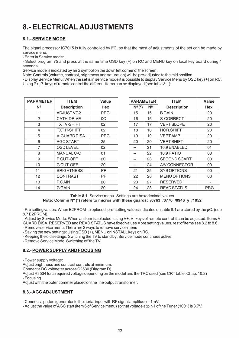
8.1.- SERVICE MODE
The signal processor IC7015 is fully controlled by I²C, so that the most of adjustments of the set can be made by service menu.- Enter in Service mode:- Select program 75 and press at the same time OSD key (+) on RC and MENU key on local key board during 4 seconds.Service mode is indicated by an S symbol on the down left corner of the screen.Note: Controls (volume, contrast, brightness and saturation) will be pre-adjusted to the mid position.- Display Service Menu: When the set is in service mode it is possible to display Service Menu by OSD key (+) on RC. Using P+, P- keys of remote control the different items can be displayed (see table 8.1):
Table 8.1. Service menu. Settings are hexadecimal valuesNote: Column Nº (*) refers to micros with these guards: /0763 /0776 /0946 y /1052
- Pre setting values: When E2PROM is replaced, pre-setting values indicated on table 8.1 are stored by the µC. (see 8.7 E2PROM).- Adjust by Service Mode: When an item is selected, using V+, V- keys of remote control it can be adjusted. Items V-GUARD DISA, RESERVED and READ STATUS have fixed values = pre setting values, rest of items see 8.2 to 8.6.- Remove service menu: There are 2 ways to remove service menu- Saving the new settings: Using OSD (+), MENU or INSTALL keys on RC.- Keeping the old settings: Switching the TV to stand by. Service mode continues active.- Remove Service Mode: Switching off the TV
8.2.- POWER SUPPLY AND FOCUSING
- Power supply voltage:Adjust brightness and contrast controls at minimum.Connect a DC voltmeter across C2530 (Diagram D).Adjust R3534 for a required voltage depending on the model and the TRC used (see CRT table, Chap. 10.2)- FocusingAdjust with the potentiometer placed on the line output transformer.
8.3.- AGC ADJUSTMENT
- Connect a pattern generator to the aerial input with RF signal amplitude = 1mV.- Adjust the value of AGC start (item 6 of Service menu) so that voltage at pin 1 of the Tuner (1001) is 3.7V.
PARAMETER ITEM Value PARAMETER ITEM Value
Nº Description Hex Nº (*) Nº Description Hex
1 ADJUST VG2 PRG 15 15 B GAIN 20
2 CATH.DRIVE 0C 16 16 S-CORRECT 20
3 TXT V-SHIFT 02 17 17 VERT.SLOPE 20
4 TXT H-SHIFT 02 18 18 HOR.SHIFT 20
5 V-GUARDDISA PRG 19 19 VERT.AMP 20
6 AGC START 25 20 20 VERT.SHIFT 20
7 OSD LEVEL 02 -- 21 16:9 ENABLED 01
8 MANUALC-O 01 -- 22 16:9 RATIO 08
9 R CUT-OFF 20 -- 23 SECOND SCART 00
10 G CUT-OFF 20 -- 24 A/V CONNECTOR 00
11 BRIGHTNESS PP 21 25 SYS OPTIONS 00
12 CONTRAST PP 22 26 MENU OPTIONS 00
13 R GAIN 20 23 27 RESERVED -
14 G GAIN 20 24 28 READ STATUS PRG
22

8.4.- WHITE D
8.4.1.- Manual cut-offItem 8 of adjusting values should be 00 (see table 8.1), that means set is in automatic cut-off. However it is possible that RGB do not start (black picture), due to grid 2 is not adjusted. In this case we recommend to change to Manual cut-off (Item 8 = 01), pre-adjust grid 2 to have a good picture and change to automatic cut-off (Item 8 = 0) before continue adjusting (see warm-up detection circuit in 7.1.5)
8.4.2.- Grid 2- Connect a white pattern generator.- Adjust contrast at 00 and brightness at 36. (00 and 24 in the service menu because hexadecimal values are used)- Put parameter 1 of the service menu ADJUST VG2 = 1. An arrow will be displayed on the left upper corner.- Adjust VG2 potentiometer (in line transformer) till the arrow will be transformed to a square.- In a few seconds, arrow will disappear and ADJUST VG2 parameter will be come back to 00.
8.4.3.- White checking- Connect pattern generator containing grey scale- Adjust the set to normal operation and reduce the saturation control to minimum.- Allow the set to warm up about 10 minutes and check visually if the grey scale has correct colour.- If not, enter to Service menu and adjust G and B gain (items 14 and 15) until a desired grey is obtained. In thecase that adjusting is difficult, start again with the setting values of table 8.1 (items 9, 10, 13, 14 and 15).
8.5.- GEOMETRY
- Connect a circle pattern generator with the controls at nominal conditions and enter to service menu.Adjust to have picture centred in vertical position by service menu item 16.- Horizontal shift:Adjust to have picture centred in horizontal position by service menu item 18.- Vertical amplitude:Adjust picture height to cover the screen by service menu item 19.Adjustments only if necessary:- TXT Shift:Vertical and horizontal shift of OSD or TXT can be adjusted by items 3 and 4 of service menu.- Vertical slope:When item 17 is selected, only upper part of the screen can be seen. Vertical slope is adjusted when centre lineof the pattern is just visible.- Vertical S correction:S correction can be adjusted by item 20 of service menu.
8.6.- OPTIONS
8.6.1.- System optionsThe chassis system is described in option SYS OPTIONS of the service menu, and the following alternatives are possible:
Table 8.2: SYSTEM OPTIONS Adjust
23
VALUE TDA93x1 - MULTI TDA93x0 - NOT MULTI
00H PAL BG PAL BG
01H PAL I PAL I
02H PAL SECAM BG PAL BG - I
03H PAL SECAM BG - DK PAL BG - DK
04H PAL SECAM BG - L - LP
05H PAL SECAM BG - I - L - LP
06H PAL SECAM BG - I - DK - L - LP

Important note: All the chassis have identification sheet when the chassis type is indicated:"Cod. service: SXXMXX", where SXX means the option of system and MXX means the option of menu
Example: S01M00 means: SYS OPTIONS = 01 (Pal I) MENU OPTIONS = 00 (16 Languages menu)
When the chassis or the EEPROM (IC7685) have to be replaced, be careful to keep the same type of chassis, setting correctly the chassis options.
If the microcontroller detects an incompatible option setting with the chassis configuration, it changes them automatically. This case is only detected first time that the TV set is switch on, and an error message E7 is displayed (see cap. 8.7). Options should be checked according to the identification label.
16:9 ENABLED VALUE
Button 16:- not respond. Not scart levels 00H
Button 16:9 functioning and Scart levels 01H
Picture 16:9 Zoom Conprese
V: 75%
8.6.3.- Option 16:9 and adjustment of screen format 16:9 (only micros with software mask /1196 and /1227)- Adjust parameter 21 (16:9 ENABLED) in order to activate/deactivate format option 16:9. By adjusting parameter 22 (16:9 RATIO), we modify format ratio 16:9.
Table 8.4: 16:9 ENABLED adjust
Fig.8.1: Format 16:9 ratio adjust
24
MENU OPTIONS VALUE MONO STEREO
Menu 00H X X
Bars 01H X
Basic Bars (NO Scart) 02H X
Stereo Menu with double Scart 03H X
Menu only UHF 04H X X
Bars only UHF 05H X
Basic Bars only UHF (NO Scart) 06H X
Stereo Menu with double Scart only UHF 07H X
8.6.2.- Menu OptionsThe various types of menus are described in MENU OPTIONS, and these include the following alternatives:
Table 8.3: MENU OPTIONS Adjust
8.6.4.- Optional connectors (stereo TV sets)Parameters 23 and 24 of the service menu allow us to configure external connections to the chassis, depending on whether we have double euroconnectors (PAR. 23 = 01) and a lateral AV connection (PAR. 24 = 01).
8.7.- PLUG & PLAY
To exit Plug&Play: 1.- Select your language and press the Menu key (or Install).2.- Press right arrow key to start tuning3.- Cancel by pressing Menu key (or Install)4.- Press Menu key (or Install) to exit the Sort Programs Menu
To enter Plug&Play:1.- Press the Local Menu key and the Install key of your remote control continuously for 4 seconds.
8.8.- ERROR MESSAGESThe microcomputer also detects errors in circuits connected to the I²C (Inter IC) bus. These error messages are communicated via OSD (On Screen Display):
25
Error message Error description Component
E1 New EEprom memory Adjust needed
E2 EEprom communication error IC 7685
E3 µC internal error (RA M) IC 7015
E4 Internal bus communication IC 7015
E5 SDA2/ SCL2 bus wrong communication IC 7701 (stereo)
No sound menu SDA2/ SCL2 bus no communication IC 7701 (stereo)
E6 EEprom data error IC 7685
E7 Not allowed options * (see 8.6) Item 21 y 22 service menu
E8 Vertical guard protection Pin 50, IC 7015
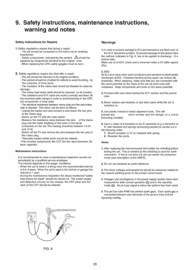
26

10. Replacement parts list CTR-AA CHASSIS
10.1 Electrical
27

10.2 Electromechanical CTR-AA CHASSIS
2
2
3
4
4
4
5
5
5
5
6
7
DEGAUSSING COIL 14”
DEGAUSSING COIL 21”
LOUDSPEAKER 3” 1.5W 25 OHMS TV 14” MONO
LOUDSPEAKER 50x90 3W 16 OHMS TV20/21 MONO
LOUDSPEAKER 50x90 3W 8 OHMS TV20/21 MONO
LOUDSPEAKER 58x126 6W 16 OHMS STEREO
REMOTE CONTROL MENU TXT
REMOTE CONTROL MENU NO TXT
REMOTE CONTROL RF25 STEREO
REMOTE CONTROL BARS NO TXT
LOOP AERIAL
ROOD AERIAL ANLY FOR EIRE
313E 108 21641
313E 108 67781
3130 100 60191
3130 100 20401
3130 100 60301
3130 100 60931
3130 108 21431
3130 108 21441
313W 108 21711
3130 108 21481
3130 100 20482
3130 100 20361
POS. DESCRIPTION CODE SAFETY
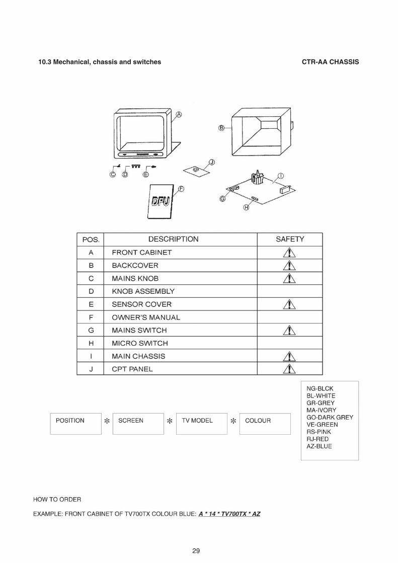
10.3 Mechanical, chassis and switches CTR-AA CHASSIS
29

313010526341


![Operation Manual Series 47K Gas Detector [SIL 2]...MSA EC DECLARATION OF CONFORMITY Series 47K Gas Detector [SIL 2] 3 EC Declaration of Conformity The manufacturer MSA AUER GmbH Thiemannstr.](https://static.fdocuments.in/doc/165x107/60d5f53bb028fb6987521b9a/operation-manual-series-47k-gas-detector-sil-2-msa-ec-declaration-of-conformity.jpg)