Sequential Circuits: Latches and FlipLatches and …zshi/course/cse2300/lecture10_latch.pdfMany...
30
Sequential Circuits: Latches and Flip-Flops Latches and Flip Flops Z. Jerry Shi Computer Science and Engineering University of Connecticut University of Connecticut Thank John Wakerly for providing his slides and figures.
Transcript of Sequential Circuits: Latches and FlipLatches and …zshi/course/cse2300/lecture10_latch.pdfMany...

Sequential Circuits:Latches and Flip-FlopsLatches and Flip Flops
Z. Jerry ShiComputer Science and Engineering
University of ConnecticutUniversity of Connecticut
Thank John Wakerly for providing his slides and figures.

Sequential circuits
• Output depends on current input and past history of inputs• How can you tell an input is current or in the past?How can you tell an input is current or in the past?
• The circuits can remember past inputs– “Memory” is needed to remember the pastMemory is needed to remember the past

Bistable element
• The simplest sequential circuit• Two statesTwo states
– One state variable, say, Q
HIGH LOW
LOW HIGH

Bistable element
• The simplest sequential circuit• Two statesTwo states
– One state variable, say, Q
LOW HIGH
HIGH LOW

Analog analysis
• Assume pure CMOS thresholds, 5 V rail• Theoretical threshold center is 2.5 V

Analog analysis
• Assume pure CMOS thresholds, 5V rail• Theoretical threshold center is 2 5 VTheoretical threshold center is 2.5 V
2.5 V 2.5 V
2 5 V 2 5 V2.5 V 2.5 V

Analog analysis
• Assume pure CMOS thresholds, 5V rail• Theoretical threshold center is 2.5 V
2 5 V2 5 V2 51 V4 8 V 2 0 V0 0 V2.5 V2.5 V2.51 V4.8 V 2.0 V0.0 V
2.5 V 2.5 V4.8 V5.0 V2.0 V0.0 V
Metastable state

Metastability
• Metastability is inherent in any bistable circuit
• Two stable points one metastable point• Two stable points, one metastable point

Control bistable
• How to control it?– Control inputs S and RControl inputs S and R
• S-R latch

S-R latch operation
Metastability is possibleif S and R are negatedif S and R are negatedsimultaneously.

S-R latch timing parameters
• Propagation delay• Minimum pulse widthMinimum pulse width

S-R latch symbols

S-R latch using NAND gates

S-R latch with enable
Let C decide whether S and R can reach the bistable circuit.reach the bistable circuit.

D latch

D-latch operation
When C = 1, Q = D.When C 1, Q D.
When C = 0, Q does not change.

D-latch timing parameters
• When C = 1, Q follows D– Propagation delay (from C or D)p g y ( )
• When C = 0, Q remembers D’s value at the 1 0 transition– Setup time (D before C’s falling edge)
ld i ( f C’ f lli d )– Hold time (D after C’s falling edge)

Positive edge-triggered D flip-flop
1 2
CLK_L QLatch 2Status
QMLatch 1Status
CLK
Dprev@ ↑Dprev@ ↑↑↓
0 QM=Dprev@ ↑EnabledDprev@ ↑Disabled1
Dprev@ ↑D
Dprev@ ↑Disabled~ DEnabled
↓
1
↑
0
QM = D @ ↑Enabled↑D@ ↑Disabled01

Positive edge-triggered D flip-flop behavior

D flip-flop timing parameters
• Propagation delay (from CLK)• Setup time (D before CLK)Setup time (D before CLK)• Hold time (D after CLK)

CMOS positive edge-triggered D flip-flop
• Two feedback loops (master and slave latches)• Uses transmission gates in feedback loops

Positive edge-triggered D flip-flop with preset and clear
• Preset and clear inputs– Like S-R latch

Negative edge-trigged D flip-flop
• Invert the input CLK signal

Positive-edge-triggered D flip-flop with enable
How does EN works?

Scan flip-flop
How is this circuit different from thedifferent from the
previous one?

Scan flip-flops -- for testing
• TE = 0 normal operation• TE = 1 test operation
All f h fli fl h k d h i d i h i f– All of the flip-flops are hooked together in a daisy chain from external test input TI.
– Load up (“scan in”) a test pattern, do one normal operation, shift p ( ) p pout (“scan out”) result on TO.

Edge-Triggered J-K flip-flop
• Not used muchmuch anymore
• Don’t worry about themabout them

T flip-flops
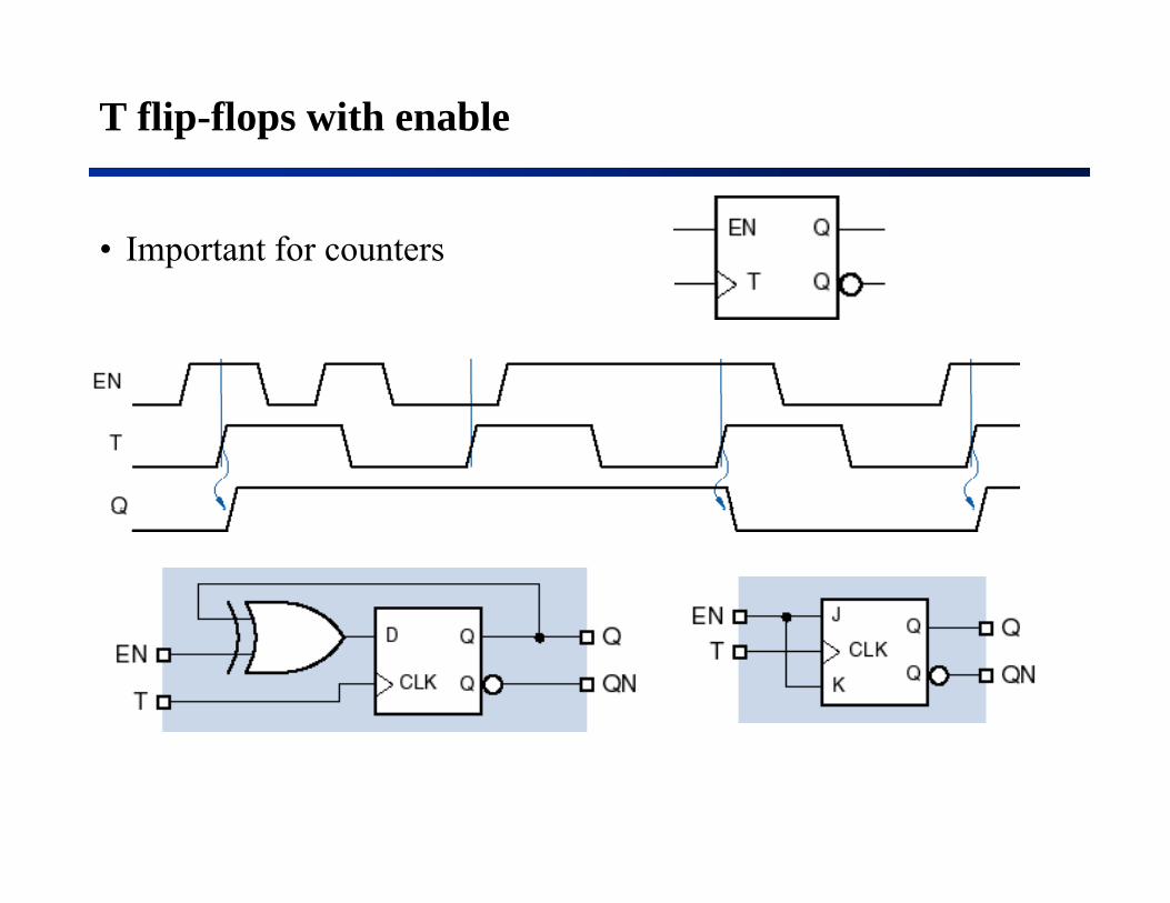
T flip-flops with enable
• Important for counters

Many types of latches and flip-flops
• S-R latch• S_L-R_L latch• S-R latch with enable• D latch• Edge-triggered D flip-flopEdge triggered D flip flop• Edge-triggered D flip-flop with enable• Edge-triggered D flip-flop with preset and clear
S fli fl• Scan flip-flop• Edge-triggered J-K flip-flop• Master/slave S-R flip-flop• Master/slave J-K flip-flop• T flip-flop• T flip-flop with enableT flip flop with enable