
Sensors and Actuators B: Chemical - users.soe.ucsc.edutyamada/Course_handouts/Bondavalli... ·...
15
Sensors and Actuators B 140 (2009) 304–318 Contents lists available at ScienceDirect Sensors and Actuators B: Chemical journal homepage: www.elsevier.com/locate/snb Review Carbon nanotubes based transistors as gas sensors: State of the art and critical review Paolo Bondavalli a,∗ , Pierre Legagneux a , Didier Pribat b a Nanocarb Laboratory, Thales Research and Technology, Palaiseau 91767, France b Laboratoire Physique Interfaces et Couches Minces (LPICM), Ecole Polytechnique, Palaiseau 91128, France article info Article history: Received 5 January 2009 Received in revised form 17 March 2009 Accepted 9 April 2009 Available online 3 May 2009 Keywords: SWCNT CNTFET Nanosensors Nanotechnology Gas sensing abstract In this paper we present recent studies concerning gas sensors based on carbon nanotube field effect transistors (CNTFETs). Although these devices have allowed one to realize sensors with an impressive sensitivity compared to existing technologies, the physical interpretation of the interaction between the gas molecules and the CNTFETs has not been clarified yet. In this contribution, we try to find some consistency between the physical interpretations advanced by the different scientific teams working on the subject and to answer some unsolved questions. Moreover, considering that the selectivity is the main issue, we analyze the different routes that have been proposed to overcome this problem: functionalization using polymers, diversification of the source/drain metal electrodes, metal decoration of SWCNT mats, exploitation of the desorption time of the different gases. For each technique we try to evaluate the advantages and the drawbacks. © 2009 Elsevier B.V. All rights reserved. Contents 1. Introduction ......................................................................................................................................... 304 2. Gas–CNTFET interaction: gas-induced doping or Schottky barrier modulation? .................................................................. 305 3. Effect of humidity on CNTFET ....................................................................................................................... 309 4. CNTFET based sensor using SWCNT mats ........................................................................................................... 309 5. Routes to improve selectivity ........................................................................................................................ 312 6. Conclusions .......................................................................................................................................... 316 References ........................................................................................................................................... 317 Biographies .......................................................................................................................................... 318 1. Introduction Carbon nanotubes (CNTs) are one-dimensional molecular struc- tures obtained by rolling up one graphene sheet into a seamless cylinder (single-wall-carbon-nanotube, i.e., SWCNT) or more (multi-wall-carbon-nanotube, i.e., MWCNT). Since their discovery in 1991 [1], many scientific teams have focused their interest on this novel material which shows extraordinary physical proper- ties. Actually, CNTs have demonstrated very high carrier mobility in field effect transistors [2], a very high electromigration threshold (10 8 –10 9 A/cm 2 [3]), a very high thermal conductivity (for a single tube, it can reach 3000 W/A K [4–6]) and exceptional mechanical ∗ Corresponding author. Tel.: +33 169415883. E-mail address: [email protected] (P. Bondavalli). properties (the measured specific tensile strength of a single shell of a MWCNT can be as high as 100 times that of steel [7]). Therefore, CNTs are studied for many applications: for field emission devices [8–12], for composites, in order to improve electrical or thermal management as well as mechanical resistance [13,14], for electronic devices, to replace silicon based transistors [15,16] and finally, for chemical and biological sensors [17–19]. Concerning this last appli- cation, different kind of gas/chemical sensors, based on different working principles, have been fabricated thanks to CNTs: miniatur- ized ionizing gas sensors (also called “micro-gun” sensors) [20], CNT thin films with variable resistance as a function of the adsorbed gas properties [21–24] and finally carbon nanotube field effect transis- tor (CNTFET) based sensors. The main advantages for CNTFET based sensors, compared to existing technologies, are numerous, since devices can be made ultra compact, effective at room temperature, with a low power consumption, a very fast response time, a low 0925-4005/$ – see front matter © 2009 Elsevier B.V. All rights reserved. doi:10.1016/j.snb.2009.04.025
Transcript of Sensors and Actuators B: Chemical - users.soe.ucsc.edutyamada/Course_handouts/Bondavalli... ·...
R
Cr
Pa
b
a
ARRAA
KSCN
ti(t
0d
Sensors and Actuators B 140 (2009) 304–318
Contents lists available at ScienceDirect
Sensors and Actuators B: Chemical
journa l homepage: www.e lsev ier .com/ locate /snb
eview
arbon nanotubes based transistors as gas sensors: State of the art and criticaleview
aolo Bondavalli a,∗, Pierre Legagneuxa, Didier Pribatb
Nanocarb Laboratory, Thales Research and Technology, Palaiseau 91767, FranceLaboratoire Physique Interfaces et Couches Minces (LPICM), Ecole Polytechnique, Palaiseau 91128, France
r t i c l e i n f o
rticle history:eceived 5 January 2009eceived in revised form 17 March 2009ccepted 9 April 2009
a b s t r a c t
In this paper we present recent studies concerning gas sensors based on carbon nanotube field effecttransistors (CNTFETs). Although these devices have allowed one to realize sensors with an impressivesensitivity compared to existing technologies, the physical interpretation of the interaction betweenthe gas molecules and the CNTFETs has not been clarified yet. In this contribution, we try to find some
vailable online 3 May 2009
eywords:WCNTNTFETanosensors
consistency between the physical interpretations advanced by the different scientific teams workingon the subject and to answer some unsolved questions. Moreover, considering that the selectivity isthe main issue, we analyze the different routes that have been proposed to overcome this problem:functionalization using polymers, diversification of the source/drain metal electrodes, metal decorationof SWCNT mats, exploitation of the desorption time of the different gases. For each technique we try to
NanotechnologyGas sensing
evaluate the advantages and the drawbacks.© 2009 Elsevier B.V. All rights reserved.
Contents
1. Introduction . . . . . . . . . . . . . . . . . . . . . . . . . . . . . . . . . . . . . . . . . . . . . . . . . . . . . . . . . . . . . . . . . . . . . . . . . . . . . . . . . . . . . . . . . . . . . . . . . . . . . . . . . . . . . . . . . . . . . . . . . . . . . . . . . . . . . . . . . 3042. Gas–CNTFET interaction: gas-induced doping or Schottky barrier modulation? . . . . . . . . . . . . . . . . . . . . . . . . . . . . . . . . . . . . . . . . . . . . . . . . . . . . . . . . . . . . . . . . . . 3053. Effect of humidity on CNTFET . . . . . . . . . . . . . . . . . . . . . . . . . . . . . . . . . . . . . . . . . . . . . . . . . . . . . . . . . . . . . . . . . . . . . . . . . . . . . . . . . . . . . . . . . . . . . . . . . . . . . . . . . . . . . . . . . . . . . . . 3094. CNTFET based sensor using SWCNT mats . . . . . . . . . . . . . . . . . . . . . . . . . . . . . . . . . . . . . . . . . . . . . . . . . . . . . . . . . . . . . . . . . . . . . . . . . . . . . . . . . . . . . . . . . . . . . . . . . . . . . . . . . . . 309
5. Routes to improve selectivity . . . . . . . . . . . . . . . . . . . . . . . . . . . . . . . . . . . . . . . . . . . . . . . . . . . . . . . . . . . . . . . . . . . . . . . . . . . . . . . . . . . . . . . . . . . . . . . . . . . . . . . . . . . . . . . . . . . . . . . . 3126. Conclusions . . . . . . . . . . . . . . . . . . . . . . . . . . . . . . . . . . . . . . . . . . . . . . . . . . . . . . . . . . . . . . . . . . . . . . . . . . . . . . . . . . . . . . . . . . . . . . . . . . . . . . . . . . . . . . . . . . . . . . . . . . . . . . . . . . . . . . . . . . 316. . . .
. . . .
ies. Actually, CNTs have demonstrated very high carrier mobilityn field effect transistors [2], a very high electromigration threshold108–109 A/cm2 [3]), a very high thermal conductivity (for a singleube, it can reach 3000 W/A K [4–6]) and exceptional mechanical
∗ Corresponding author. Tel.: +33 169415883.E-mail address: [email protected] (P. Bondavalli).
925-4005/$ – see front matter © 2009 Elsevier B.V. All rights reserved.oi:10.1016/j.snb.2009.04.025
. . . . . . . . . . . . . . . . . . . . . . . . . . . . . . . . . . . . . . . . . . . . . . . . . . . . . . . . . . . . . . . . . . . . . . . . . 317
. . . . . . . . . . . . . . . . . . . . . . . . . . . . . . . . . . . . . . . . . . . . . . . . . . . . . . . . . . . . . . . . . . . . . . . . . 318
properties (the measured specific tensile strength of a single shellof a MWCNT can be as high as 100 times that of steel [7]). Therefore,CNTs are studied for many applications: for field emission devices[8–12], for composites, in order to improve electrical or thermalmanagement as well as mechanical resistance [13,14], for electronicdevices, to replace silicon based transistors [15,16] and finally, forchemical and biological sensors [17–19]. Concerning this last appli-cation, different kind of gas/chemical sensors, based on differentworking principles, have been fabricated thanks to CNTs: miniatur-ized ionizing gas sensors (also called “micro-gun” sensors) [20], CNTthin films with variable resistance as a function of the adsorbed gasproperties [21–24] and finally carbon nanotube field effect transis-
References . . . . . . . . . . . . . . . . . . . . . . . . . . . . . . . . . . . . . . . . . . . . . . . . . . . . . . . . . . . . . .Biographies . . . . . . . . . . . . . . . . . . . . . . . . . . . . . . . . . . . . . . . . . . . . . . . . . . . . . . . . . . . . .
1. Introduction
Carbon nanotubes (CNTs) are one-dimensional molecular struc-tures obtained by rolling up one graphene sheet into a seamlesscylinder (single-wall-carbon-nanotube, i.e., SWCNT) or more(multi-wall-carbon-nanotube, i.e., MWCNT). Since their discoveryin 1991 [1], many scientific teams have focused their interest onthis novel material which shows extraordinary physical proper-
tor (CNTFET) based sensors. The main advantages for CNTFET basedsensors, compared to existing technologies, are numerous, sincedevices can be made ultra compact, effective at room temperature,with a low power consumption, a very fast response time, a low

P. Bondavalli et al. / Sensors and Actuators B 140 (2009) 304–318 305
Fig. 1. Transfer characteristic change after exposure to NO2 and NH3 of the firstCei7
rtcosc[t
Fptatitovmsxt
2b
gKucw(uaoatg
rro
NTFET gas sensor fabricated at Stanford in 2000 by Kong et al. [26]. Gas-sensingxperiments were carried out by placing CNTFETs into a sealed glass flask and expos-ng to NO2 [2–200 parts per million (ppm)] or NH3 (0.1–1%) in Ar or air (flow rate of00 ml/min). The channel length was around 5 �m.
ecovery time (few seconds) and they show a good versatility (i.e.,hey can be used for several gases). Finally relatively low fabricationosts can be reached, considering that CMOS compatible technol-gy can be employed. It has to be pointed out that for this kind ofensors, the research has essentially focused on SWCNTs (whichan be semiconducting or metallic, depending on their chirality25]) because MWCNTs are only metallic and therefore unsuitableo fabricate transistors.
This paper deals with the state of the art in the domain of CNT-ET based gas/chemical sensors and intends to review the differenthysical arguments developed to explain the gas/device interac-ion, trying to find some consistency between them, in order tonswer the different unsolved questions. A section is devoted tohe different routes developed to improve selectivity. This is a verymportant issue, considering that a high selectivity is the key factoro definitively strike huge markets such as security (e.g., detectionf warfare gases such as nerve agents or detection of traces of highlyolatile and explosive gases), healthcare (e.g., NO sensors for asthmaonitoring or CO2 for emergency airway management), safety (e.g.,
ensors for the detection CO or benzene, toluene, ethylbenzene, andylenes, commonly called BTEX group) and environmental moni-oring (e.g., NO2, benzene).
. Gas–CNTFET interaction: gas-induced doping or Schottkyarrier modulation?
The first paper showing the great potentiality of CNTFETs foras sensing applications was published in 2000 [26]. In this paperong et al. at Stanford University observed that a single SWCNTsed as a transistor channel between two gold electrodes, fabri-ated on a SiO2/Si substrate acting as a bottom gate, interactedith gas molecules, changing the CNTFET transfer characteristics
source-to-drain current as a function of the gate voltage). The gasessed for tests were NO2 and NH3 with concentrations between 2nd 10,000 ppm. These gases were chosen because they exhibit twopposite electronic behaviours as a consequence of their chemicalffinity: the first one is an “electron-acceptor” gas (thus inducing p-ype doping of the SWNT) and the second one is an “electron-donor”
as (inducing n-type doping).The experimental results pointed out an increase and aeduction of the p-type CNTFET conductance for NO2 and NH3,espectively (Fig. 1). Concerning NO2, its interaction with the nan-tube was interpreted as strictly connected to a bulk doping effect.
Fig. 2. Configurations of CNTFETs for the tests performed at the University of SouthCalifornia by Liu et al. Schematics showing the CNTFET zones exposed to gas species:(a) center-covered configuration, (b) contact-covered configuration [31].
Actually, NO2 can be bound to a semiconducting nanotube with asubsequent electron charge transfer from the tube to the adsorbedmolecules [27–30]: the hole carrier concentration in the nanotubeincreases and so does the conductance, with a consequent shift ofthe activation bias (VON) to a larger positive voltage. This effect hasbeen assimilated to a sort of “molecular gating” of the carbon nan-otube, due to the gas molecules adsorption. On the contrary, NH3molecules, as it has been demonstrated, have no binding affinitywith semiconducting SWCNTs [27–30]. The Stanford team invokedtwo possible reasons in order to explain the effect of the NH3molecules on the CNTFET channel:
• The binding between NH3 molecules and the hydroxyl groups onthe SiO2 substrate leading to a reduction of the negative chargeson the oxide and equivalent to a positive electrostatic gating ofthe SWCNT.
• The interaction of NH3 with oxygen species adsorbed on SWCNT.
Liu et al. at the University of Southern California (USC) [31], per-formed in 2005 measurements on the same type of devices testedby Kong et al. at Stanford, and constituted by a single SWCNT asCNTFET channel. Experimental tests were performed on the CNT-FET exposed to concentrations varying from 0 to 4 ppm of NO2 andfrom 0 to 400 ppm of NH3, covering alternatively the metal/SWCNTcontacts and the center of the channel (Fig. 2) with polymethyl-methacrylate (PMMA) resist. In both cases, the results showed anincrease of the VON for NO2 (shift to higher positive value) and areduction of the VON (shift to higher negative value) for NH3 (Fig. 3).These results were explained as before [26], by calling upon the dop-ing of the SWCNT (for the NH3 as well, in spite of the weak NH3–CNTbinding). The conclusion of the USC researchers was that the CNT-FETs were sensitive to gas exposure even if metal/CNT junctionswere covered.
Qualitatively, the results of Liu et al. and those of Kong et al.are similar. The main difference probably concerns the recovery
time between two successive measurements. In fact, the Stanfordteam succeeded in recovering the initial transistors characteristicsby heating the sample during 1 h at 200 ◦C in air or by exposing thesample to pure Ar (at room temperature) for around 12 h. In a dif-ferent way, for nearly the same gas concentrations, the USC team
306 P. Bondavalli et al. / Sensors and Actuators B 140 (2009) 304–318
F t al. ic d sidec
llgsgofititPtst
aoaidss
br(mtetttcroqlfmtoe
iwtgttb
gen) allowed one to obtain an n-type SWCNT and not an intrinsicone. Moreover, supposing that the SWCNT was originally dopedby oxygen, the change of oxygen concentration, and so of doping,would have given rise to a shift of the VON of the CNTFET. Actually,
Fig. 4. Results of the tests performed at Georgestown University by Zhang et al.Transfer characteristics change for a CNTFET in contact-covered configuration (a) andfully covered (b) for different exposure times to NO2 [32]. The channel was around6 �m long. The principal effect seems to be related to the interaction between thegas specie and the metal/SWCNT junctions. In both cases there is no measurablechange of the transfer characteristics during the first 30 min of exposure. After this
ig. 3. Results of the tests performed at the University of South California by Liu eovered configuration (left hand side) and contact-covered configuration (right hanharacteristics for both configurations (see text for comments).
eft the samples for 30 min in air to recover the initial signal. Thisast detail could be a very important issue because it might haveiven rise to a misinterpretation of the experimental results: a toohort recovery time could not allow the complete desorption ofas molecules on the carbon nanotubes or on the oxide after previ-us measurements. These adsorbed molecules may have altered thenal results. Also, in the situation where the contacts were covered,he extent of the passivation region from the contact was not spec-fied in Liu’s experiments, which can be an important parameter toake into account since the interface between the nanotube and theMMA certainly acts as a short circuit for gas diffusion to the con-act area. In other words, there should be a difference between theituation where the contacts are covered and the situation wherehe body of the nanotube is covered (see below).
Up to now, we have analyzed the works of research teams thatttribute the key role in the CNTFET sensing essentially to the bodyf the nanotube and not to the metal/SWCNT junctions. In fact, theyssert that the gas molecules dope the nanotube and so changets conductance. However, several scientific teams have adopted aifferent point of view and have focused their studies on demon-trating that the metal/SWCNT junctions are the key players in theensing mechanism.
In this context, one of the most interesting studies has recentlyeen published by Georgestown University [32]. In 2006, they fab-icated CNTFETs using two Pd electrodes on a SiO2/Si substratebottom gate configuration). In order to evaluate the effect of
etal/SWCNT contacts, they covered these contacts with a 200 nm-hick layer of PMMA, followed by a 2 �m-thick layer of SU8, anpoxy-based photoresist (Fig. 4a). After having exposed the CNTFETo a concentration of NO2 increasing up to 200 ppm (NO2 was mixedo N2 at atmospheric pressure), they did not observe any change inhe transfer characteristic of the CNTFET during the first 30 min,ompared to their results in ambient air. After 30 min, the satu-ated conductance increased very slowly with time. This changef conductance was interpreted and modeled as the direct conse-uence of the diffusion of the gas molecules through the polymerayers, down to the contact regions. The same result was obtainedor a wholly covered device (Fig. 4b), demonstrating that the NO2
olecules had no doping effect on the channel of the CNTFET. Forhese measurements, the total recovery time was around one dayf CNTFET exposure to ambient air, which is consistent with thexperiments of Kong et al. [26].
Another team that has been working for 10 years on CNTFETssues, is the IBM team in Yorktown Heights, led by Avouris. Their
ork, even if not focused on sensor issues, is an important con-
ribution for the understanding of the effect of oxygen, and moreenerally of gases, on the behaviour of CNTFETs. They underscoredhat CNTFETs operate as unconventional Schottky-barrier transis-ors and that the effect of adsorbed gases, e.g., O2, can be explainedy their influence on the metal electrode work-functions. The IBMn 2005, after exposure to different concentrations of NO2 and NH3 for the center-) [31]. The SWCNT was 4 �m long. The measurements show a change of the transfer
team demonstrated that if a CNTFET (exhibiting a p-type behaviourin air) was annealed in vacuum at 600 K for several minutes, it con-verted to an n-type device. They asserted that this phenomenoncould not be explained by oxygen doping [33–35]. Indeed, assum-ing that the carbon nanotube was initially p doped by oxygen, theycould not to explain why the annealing (supposed to desorb oxy-
period of time NO2 molecules reach the transistor contacts, diffusing through thePMMA and SU-8, and change the CNTFET response. The characteristics for 141 and88 min of exposure to NO2 are very similar in (a) and (b) respectively, i.e., whetherthe body of the nanotube is covered or not. This indicates that there is no dopingeffect of the NO2 molecules on the SWCNT. These results are in contradiction withthose of Liu et al. [31].
P. Bondavalli et al. / Sensors and Actuators B 140 (2009) 304–318 307
F teristia c chanc
tShtieooitI
ib
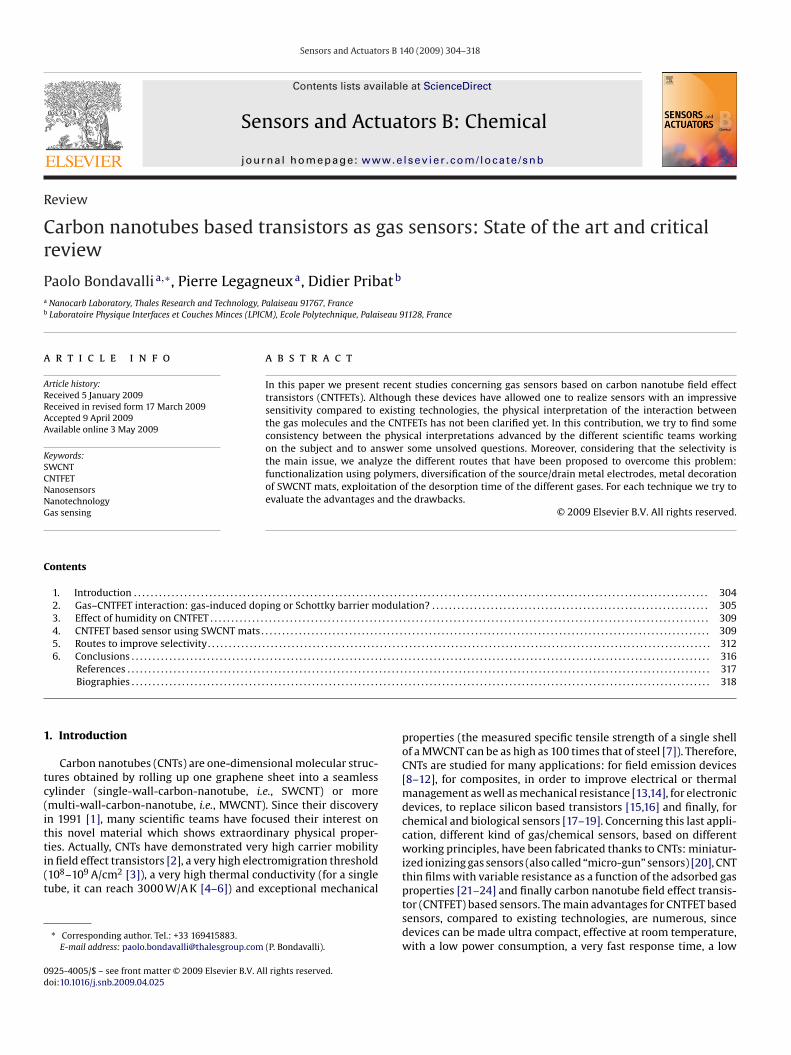
ig. 5. Tests and simulations performed at IBM by Heinze et al. (a) Transfer characs a function of potassium doping level. (c) Simulation of the transfer characteristiharacteristic change as a function of the doping level change [35].
his was not observed: the off bias interval was unchanged (Fig. 5).tarting form these observations, IBM researchers formulated theypothesis that the gas molecules adsorption changed the value ofhe Schottky barrier built-up between the SWCNT and the metaln the contact region. To check this hypothesis, they simulated theffect on the CNTFET transfer characteristics caused by the changef the metal work function, as a consequence of the adsorption ofxygen. At the same time they simulated the effect of an “hypothet-cal” CNTFET oxygen doping. The results have been compared with
he experimental ones and have unquestionably demonstrated theBM hypothesis (Fig. 5).In other studies performed by the same research team [36,37],t has been explained that the interaction of oxygen at the junctionetween the metal electrode and the SWCNT, changes the metal
Fig. 6. Effect of Oxygen on the Fermi levels alignment: (a) Au/CNT contact i
c change as a function of oxygen concentration. (b) Transfer characteristic changege as a function of the metal work function change. (d) Simulation of the transfer
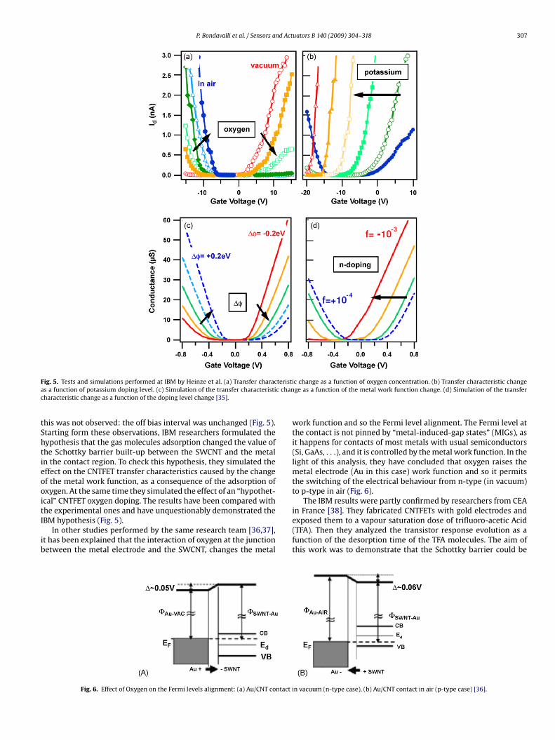
work function and so the Fermi level alignment. The Fermi level atthe contact is not pinned by “metal-induced-gap states” (MIGs), asit happens for contacts of most metals with usual semiconductors(Si, GaAs, . . .), and it is controlled by the metal work function. In thelight of this analysis, they have concluded that oxygen raises themetal electrode (Au in this case) work function and so it permitsthe switching of the electrical behaviour from n-type (in vacuum)to p-type in air (Fig. 6).
The IBM results were partly confirmed by researchers from CEA
in France [38]. They fabricated CNTFETs with gold electrodes andexposed them to a vapour saturation dose of trifluoro-acetic Acid(TFA). Then they analyzed the transistor response evolution as afunction of the desorption time of the TFA molecules. The aim ofthis work was to demonstrate that the Schottky barrier could ben vacuum (n-type case), (b) Au/CNT contact in air (p-type case) [36].
308 P. Bondavalli et al. / Sensors and Actuators B 140 (2009) 304–318
Fig. 7. Transfer characteristics of a CNTFET exposed to different concentrations oftilt
ssit
••
cbacb
cthtc
imtioqmpTuwa
leccattmtreb
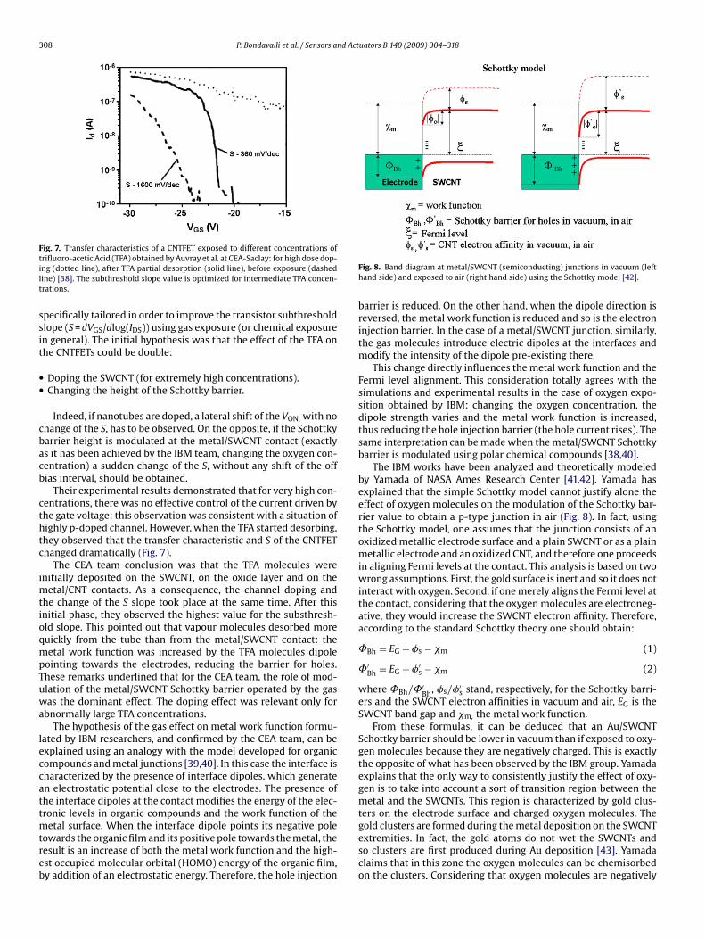
rifluoro-acetic Acid (TFA) obtained by Auvray et al. at CEA-Saclay: for high dose dop-ng (dotted line), after TFA partial desorption (solid line), before exposure (dashedine) [38]. The subthreshold slope value is optimized for intermediate TFA concen-rations.
pecifically tailored in order to improve the transistor subthresholdlope (S = dVGS/dlog(IDS)) using gas exposure (or chemical exposuren general). The initial hypothesis was that the effect of the TFA onhe CNTFETs could be double:
Doping the SWCNT (for extremely high concentrations).Changing the height of the Schottky barrier.
Indeed, if nanotubes are doped, a lateral shift of the VON, with nohange of the S, has to be observed. On the opposite, if the Schottkyarrier height is modulated at the metal/SWCNT contact (exactlys it has been achieved by the IBM team, changing the oxygen con-entration) a sudden change of the S, without any shift of the offias interval, should be obtained.
Their experimental results demonstrated that for very high con-entrations, there was no effective control of the current driven byhe gate voltage: this observation was consistent with a situation ofighly p-doped channel. However, when the TFA started desorbing,hey observed that the transfer characteristic and S of the CNTFEThanged dramatically (Fig. 7).
The CEA team conclusion was that the TFA molecules werenitially deposited on the SWCNT, on the oxide layer and on the
etal/CNT contacts. As a consequence, the channel doping andhe change of the S slope took place at the same time. After thisnitial phase, they observed the highest value for the substhresh-ld slope. This pointed out that vapour molecules desorbed moreuickly from the tube than from the metal/SWCNT contact: theetal work function was increased by the TFA molecules dipole
ointing towards the electrodes, reducing the barrier for holes.hese remarks underlined that for the CEA team, the role of mod-lation of the metal/SWCNT Schottky barrier operated by the gasas the dominant effect. The doping effect was relevant only for
bnormally large TFA concentrations.The hypothesis of the gas effect on metal work function formu-
ated by IBM researchers, and confirmed by the CEA team, can bexplained using an analogy with the model developed for organicompounds and metal junctions [39,40]. In this case the interface isharacterized by the presence of interface dipoles, which generaten electrostatic potential close to the electrodes. The presence ofhe interface dipoles at the contact modifies the energy of the elec-ronic levels in organic compounds and the work function of the
etal surface. When the interface dipole points its negative poleowards the organic film and its positive pole towards the metal, theesult is an increase of both the metal work function and the high-st occupied molecular orbital (HOMO) energy of the organic film,y addition of an electrostatic energy. Therefore, the hole injection
Fig. 8. Band diagram at metal/SWCNT (semiconducting) junctions in vacuum (lefthand side) and exposed to air (right hand side) using the Schottky model [42].
barrier is reduced. On the other hand, when the dipole direction isreversed, the metal work function is reduced and so is the electroninjection barrier. In the case of a metal/SWCNT junction, similarly,the gas molecules introduce electric dipoles at the interfaces andmodify the intensity of the dipole pre-existing there.
This change directly influences the metal work function and theFermi level alignment. This consideration totally agrees with thesimulations and experimental results in the case of oxygen expo-sition obtained by IBM: changing the oxygen concentration, thedipole strength varies and the metal work function is increased,thus reducing the hole injection barrier (the hole current rises). Thesame interpretation can be made when the metal/SWCNT Schottkybarrier is modulated using polar chemical compounds [38,40].
The IBM works have been analyzed and theoretically modeledby Yamada of NASA Ames Research Center [41,42]. Yamada hasexplained that the simple Schottky model cannot justify alone theeffect of oxygen molecules on the modulation of the Schottky bar-rier value to obtain a p-type junction in air (Fig. 8). In fact, usingthe Schottky model, one assumes that the junction consists of anoxidized metallic electrode surface and a plain SWCNT or as a plainmetallic electrode and an oxidized CNT, and therefore one proceedsin aligning Fermi levels at the contact. This analysis is based on twowrong assumptions. First, the gold surface is inert and so it does notinteract with oxygen. Second, if one merely aligns the Fermi level atthe contact, considering that the oxygen molecules are electroneg-ative, they would increase the SWCNT electron affinity. Therefore,according to the standard Schottky theory one should obtain:
˚Bh = EG + �s − �m (1)
˚′Bh = EG + �′
s − �m (2)
where ˚Bh/˚′Bh, �s/�′
s stand, respectively, for the Schottky barri-ers and the SWCNT electron affinities in vacuum and air, EG is theSWCNT band gap and �m, the metal work function.
From these formulas, it can be deduced that an Au/SWCNTSchottky barrier should be lower in vacuum than if exposed to oxy-gen molecules because they are negatively charged. This is exactlythe opposite of what has been observed by the IBM group. Yamadaexplains that the only way to consistently justify the effect of oxy-gen is to take into account a sort of transition region between themetal and the SWCNTs. This region is characterized by gold clus-ters on the electrode surface and charged oxygen molecules. The
gold clusters are formed during the metal deposition on the SWCNTextremities. In fact, the gold atoms do not wet the SWCNTs andso clusters are first produced during Au deposition [43]. Yamadaclaims that in this zone the oxygen molecules can be chemisorbedon the clusters. Considering that oxygen molecules are negatively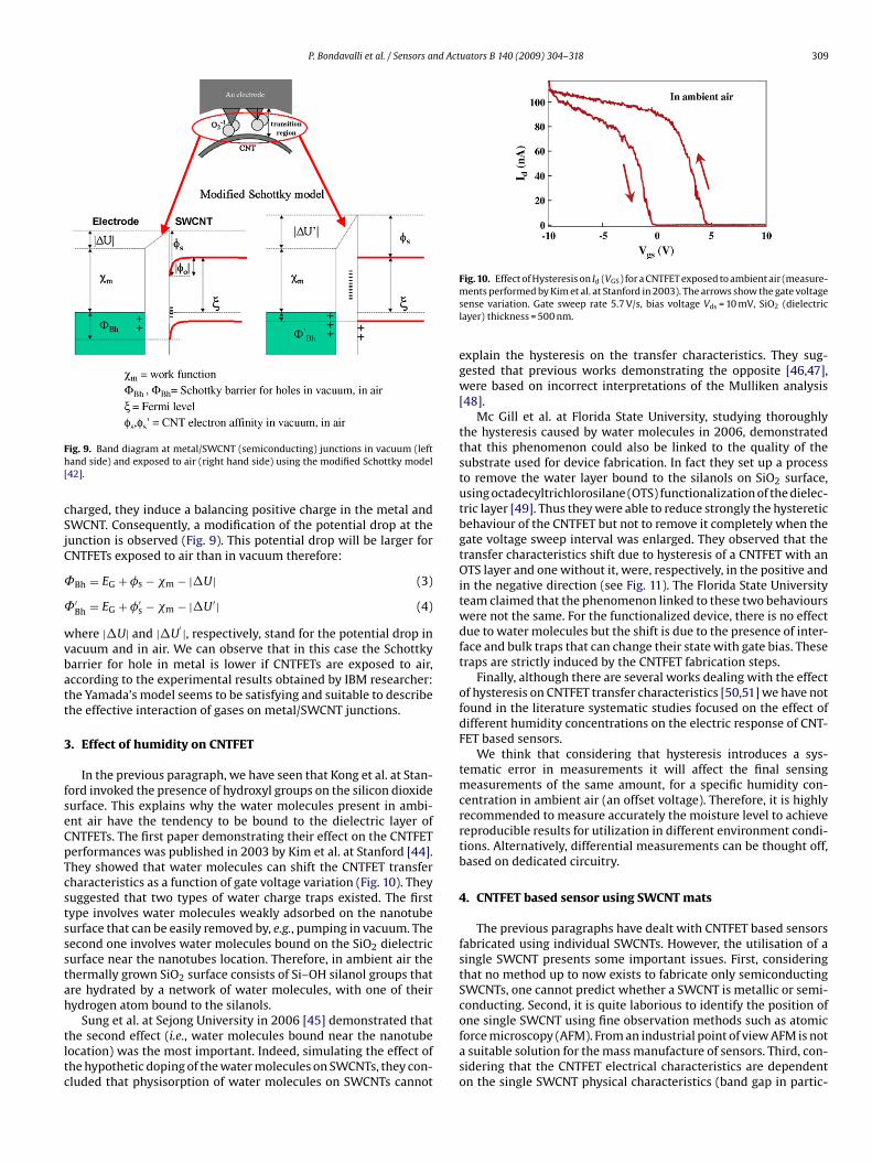
P. Bondavalli et al. / Sensors and Actuators B 140 (2009) 304–318 309
Fh[
cSjC
˚
˚
wvbatt
3
fseCpTcstssstah
tltc
ig. 9. Band diagram at metal/SWCNT (semiconducting) junctions in vacuum (leftand side) and exposed to air (right hand side) using the modified Schottky model42].
harged, they induce a balancing positive charge in the metal andWCNT. Consequently, a modification of the potential drop at theunction is observed (Fig. 9). This potential drop will be larger forNTFETs exposed to air than in vacuum therefore:
Bh = EG + �s − �m − |�U| (3)
′Bh = EG + �′
s − �m − |�U ′| (4)
here |�U| and |�U′ |, respectively, stand for the potential drop in
acuum and in air. We can observe that in this case the Schottkyarrier for hole in metal is lower if CNTFETs are exposed to air,ccording to the experimental results obtained by IBM researcher:he Yamada’s model seems to be satisfying and suitable to describehe effective interaction of gases on metal/SWCNT junctions.
. Effect of humidity on CNTFET
In the previous paragraph, we have seen that Kong et al. at Stan-ord invoked the presence of hydroxyl groups on the silicon dioxideurface. This explains why the water molecules present in ambi-nt air have the tendency to be bound to the dielectric layer ofNTFETs. The first paper demonstrating their effect on the CNTFETerformances was published in 2003 by Kim et al. at Stanford [44].hey showed that water molecules can shift the CNTFET transferharacteristics as a function of gate voltage variation (Fig. 10). Theyuggested that two types of water charge traps existed. The firstype involves water molecules weakly adsorbed on the nanotubeurface that can be easily removed by, e.g., pumping in vacuum. Theecond one involves water molecules bound on the SiO2 dielectricurface near the nanotubes location. Therefore, in ambient air thehermally grown SiO2 surface consists of Si–OH silanol groups thatre hydrated by a network of water molecules, with one of theirydrogen atom bound to the silanols.
Sung et al. at Sejong University in 2006 [45] demonstrated thathe second effect (i.e., water molecules bound near the nanotubeocation) was the most important. Indeed, simulating the effect ofhe hypothetic doping of the water molecules on SWCNTs, they con-luded that physisorption of water molecules on SWCNTs cannot
Fig. 10. Effect of Hysteresis on Id (VGS) for a CNTFET exposed to ambient air (measure-ments performed by Kim et al. at Stanford in 2003). The arrows show the gate voltagesense variation. Gate sweep rate 5.7 V/s, bias voltage Vds = 10 mV, SiO2 (dielectriclayer) thickness = 500 nm.
explain the hysteresis on the transfer characteristics. They sug-gested that previous works demonstrating the opposite [46,47],were based on incorrect interpretations of the Mulliken analysis[48].
Mc Gill et al. at Florida State University, studying thoroughlythe hysteresis caused by water molecules in 2006, demonstratedthat this phenomenon could also be linked to the quality of thesubstrate used for device fabrication. In fact they set up a processto remove the water layer bound to the silanols on SiO2 surface,using octadecyltrichlorosilane (OTS) functionalization of the dielec-tric layer [49]. Thus they were able to reduce strongly the hystereticbehaviour of the CNTFET but not to remove it completely when thegate voltage sweep interval was enlarged. They observed that thetransfer characteristics shift due to hysteresis of a CNTFET with anOTS layer and one without it, were, respectively, in the positive andin the negative direction (see Fig. 11). The Florida State Universityteam claimed that the phenomenon linked to these two behaviourswere not the same. For the functionalized device, there is no effectdue to water molecules but the shift is due to the presence of inter-face and bulk traps that can change their state with gate bias. Thesetraps are strictly induced by the CNTFET fabrication steps.
Finally, although there are several works dealing with the effectof hysteresis on CNTFET transfer characteristics [50,51] we have notfound in the literature systematic studies focused on the effect ofdifferent humidity concentrations on the electric response of CNT-FET based sensors.
We think that considering that hysteresis introduces a sys-tematic error in measurements it will affect the final sensingmeasurements of the same amount, for a specific humidity con-centration in ambient air (an offset voltage). Therefore, it is highlyrecommended to measure accurately the moisture level to achievereproducible results for utilization in different environment condi-tions. Alternatively, differential measurements can be thought off,based on dedicated circuitry.
4. CNTFET based sensor using SWCNT mats
The previous paragraphs have dealt with CNTFET based sensorsfabricated using individual SWCNTs. However, the utilisation of asingle SWCNT presents some important issues. First, consideringthat no method up to now exists to fabricate only semiconductingSWCNTs, one cannot predict whether a SWCNT is metallic or semi-conducting. Second, it is quite laborious to identify the position ofone single SWCNT using fine observation methods such as atomic
force microscopy (AFM). From an industrial point of view AFM is nota suitable solution for the mass manufacture of sensors. Third, con-sidering that the CNTFET electrical characteristics are dependenton the single SWCNT physical characteristics (band gap in partic-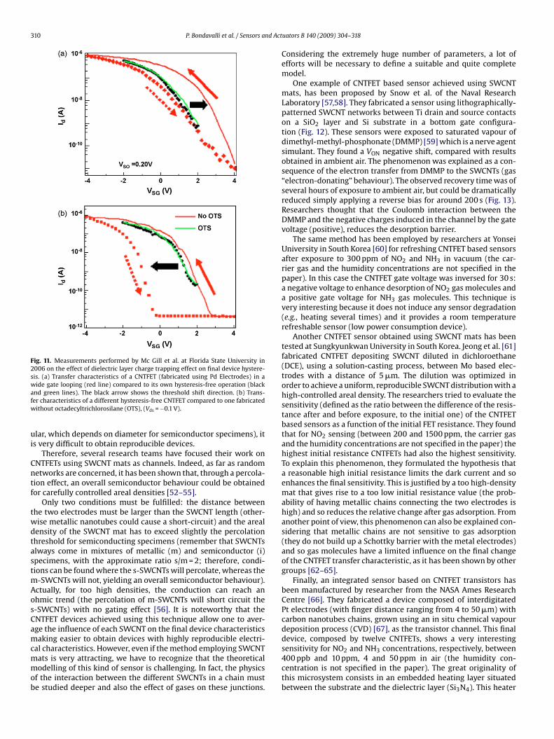
310 P. Bondavalli et al. / Sensors and Act
Fig. 11. Measurements performed by Mc Gill et al. at Florida State University in2006 on the effect of dielectric layer charge trapping effect on final device hystere-sis. (a) Transfer characteristics of a CNTFET (fabricated using Pd Electrodes) in awafw
ui
Cntf
twdtastmAosCamcmmob
sensitivity for NO and NH concentrations, respectively, between
ide gate looping (red line) compared to its own hysteresis-free operation (blacknd green lines). The black arrow shows the threshold shift direction. (b) Trans-er characteristics of a different hysteresis-free CNTFET compared to one fabricatedithout octadecyltrichlorosilane (OTS), (Vds = −0.1 V).
lar, which depends on diameter for semiconductor specimens), its very difficult to obtain reproducible devices.
Therefore, several research teams have focused their work onNTFETs using SWCNT mats as channels. Indeed, as far as randometworks are concerned, it has been shown that, through a percola-ion effect, an overall semiconductor behaviour could be obtainedor carefully controlled areal densities [52–55].
Only two conditions must be fulfilled: the distance betweenhe two electrodes must be larger than the SWCNT length (other-ise metallic nanotubes could cause a short-circuit) and the arealensity of the SWCNT mat has to exceed slightly the percolationhreshold for semiconducting specimens (remember that SWCNTslways come in mixtures of metallic (m) and semiconductor (i)pecimens, with the approximate ratio s/m = 2; therefore, condi-ions can be found where the s-SWCNTs will percolate, whereas the
-SWCNTs will not, yielding an overall semiconductor behaviour).ctually, for too high densities, the conduction can reach anhmic trend (the percolation of m-SWCNTs will short circuit the-SWCNTs) with no gating effect [56]. It is noteworthy that theNTFET devices achieved using this technique allow one to aver-ge the influence of each SWCNT on the final device characteristicsaking easier to obtain devices with highly reproducible electri-
al characteristics. However, even if the method employing SWCNT
ats is very attracting, we have to recognize that the theoreticalodelling of this kind of sensor is challenging. In fact, the physicsf the interaction between the different SWCNTs in a chain muste studied deeper and also the effect of gases on these junctions.
uators B 140 (2009) 304–318
Considering the extremely huge number of parameters, a lot ofefforts will be necessary to define a suitable and quite completemodel.
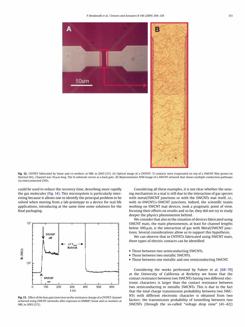
One example of CNTFET based sensor achieved using SWCNTmats, has been proposed by Snow et al. of the Naval ResearchLaboratory [57,58]. They fabricated a sensor using lithographically-patterned SWCNT networks between Ti drain and source contactson a SiO2 layer and Si substrate in a bottom gate configura-tion (Fig. 12). These sensors were exposed to saturated vapour ofdimethyl-methyl-phosphonate (DMMP) [59] which is a nerve agentsimulant. They found a VON negative shift, compared with resultsobtained in ambient air. The phenomenon was explained as a con-sequence of the electron transfer from DMMP to the SWCNTs (gas“electron-donating” behaviour). The observed recovery time was ofseveral hours of exposure to ambient air, but could be dramaticallyreduced simply applying a reverse bias for around 200 s (Fig. 13).Researchers thought that the Coulomb interaction between theDMMP and the negative charges induced in the channel by the gatevoltage (positive), reduces the desorption barrier.
The same method has been employed by researchers at YonseiUniversity in South Korea [60] for refreshing CNTFET based sensorsafter exposure to 300 ppm of NO2 and NH3 in vacuum (the car-rier gas and the humidity concentrations are not specified in thepaper). In this case the CNTFET gate voltage was inversed for 30 s:a negative voltage to enhance desorption of NO2 gas molecules anda positive gate voltage for NH3 gas molecules. This technique isvery interesting because it does not induce any sensor degradation(e.g., heating several times) and it provides a room temperaturerefreshable sensor (low power consumption device).
Another CNTFET sensor obtained using SWCNT mats has beentested at Sungkyunkwan University in South Korea. Jeong et al. [61]fabricated CNTFET depositing SWCNT diluted in dichloroethane(DCE), using a solution-casting process, between Mo based elec-trodes with a distance of 5 �m. The dilution was optimized inorder to achieve a uniform, reproducible SWCNT distribution with ahigh-controlled areal density. The researchers tried to evaluate thesensitivity (defined as the ratio between the difference of the resis-tance after and before exposure, to the initial one) of the CNTFETbased sensors as a function of the initial FET resistance. They foundthat for NO2 sensing (between 200 and 1500 ppm, the carrier gasand the humidity concentrations are not specified in the paper) thehighest initial resistance CNTFETs had also the highest sensitivity.To explain this phenomenon, they formulated the hypothesis thata reasonable high initial resistance limits the dark current and soenhances the final sensitivity. This is justified by a too high-densitymat that gives rise to a too low initial resistance value (the prob-ability of having metallic chains connecting the two electrodes ishigh) and so reduces the relative change after gas adsorption. Fromanother point of view, this phenomenon can also be explained con-sidering that metallic chains are not sensitive to gas adsorption(they do not build up a Schottky barrier with the metal electrodes)and so gas molecules have a limited influence on the final changeof the CNTFET transfer characteristic, as it has been shown by othergroups [62–65].
Finally, an integrated sensor based on CNTFET transistors hasbeen manufactured by researcher from the NASA Ames ResearchCentre [66]. They fabricated a device composed of interdigitatedPt electrodes (with finger distance ranging from 4 to 50 �m) withcarbon nanotubes chains, grown using an in situ chemical vapourdeposition process (CVD) [67], as the transistor channel. This finaldevice, composed by twelve CNTFETs, shows a very interesting
2 3400 ppb and 10 ppm, 4 and 50 ppm in air (the humidity con-centration is not specified in the paper). The great originality ofthis microsystem consists in an embedded heating layer situatedbetween the substrate and the dielectric layer (Si3N4). This heater
P. Bondavalli et al. / Sensors and Actuators B 140 (2009) 304–318 311
F cal imt presev
ctesafi
FaN
ig. 12. CNTFET fabricated by Snow and co-workers at NRL in 2003 [57]. (A) Optihermal SiO2. Channel was 10 �m long. The Si substrate serves as a back gate. (B) Reia interconnected CNTs.
ould be used to reduce the recovery time, desorbing more rapidlyhe gas molecules (Fig. 14). This microsystem is particularly inter-
sting because it allows one to identify the principal problem to beolved when moving from a lab prototype to a device for real lifepplications, introducing at the same time some solutions for thenal packaging.ig. 13. Effect of the bias gate inversion on the resistance change of a CNTFET channelchieved using SWCNT networks after exposure to DMMP (Snow and co-workers atRL in 2003 [57]).
age of a CNTFET: Ti contacts were evaporated on top of a SWCNT film grown onntative AFM image of a SWCNT network that shows multiple conduction pathways
Considering all these examples, it is not clear whether the sens-ing mechanism in a mat is still due to the interaction of gas specieswith metal/SWCNT junctions or with the SWCNTs mat itself, i.e.,with m-SWCNT/s-SWCNT junctions. Indeed, the scientific teamsworking on SWCNT mat devices, took a pragmatic point of view,focusing their efforts on results and so far, they did not try to studydeeper the physics phenomenon behind.
We consider that also in the situation of devices fabricated usingSWCNT mats, the main phenomenon, at least for channel lengthsbelow 100 �m, is the interaction of gas with Metal/SWCNT junc-tions. Several considerations allow us to support this hypothesis.
We can observe that in CNTFETs fabricated using SWCNT mats,three types of electric contacts can be identified:
• Those between two semiconducting SWCNTs.• Those between two metallic SWCNTs.• Those between one metallic and one semiconducting SWCNT.
Considering the works performed by Fuhrer et al. [68–70]at the University of California at Berkeley we know that thecontact resistance between two SWCNTs having two different elec-tronic characters is larger than the contact resistance between
two semiconducting or metallic SWCNTs. This is due to the factthat the total charge transmission probability between two SWC-NTs with different electronic character is obtained from twofactors: the transmission probability of tunnelling between twoSWCNTs (through the so-called “voltage drop zone” [41–42])
312 P. Bondavalli et al. / Sensors and Actuators B 140 (2009) 304–318
ed sen
aSat[flS
atnbewc
ttnHstt
bt(
Fig. 14. Schematic view of the different layers composing the integrat
nd the transmission probability of the tunnelling through thechottky barrier when it exists (contact between a metallicnd a semiconducting nanotube). The result is a contact resis-ance two orders of magnitude larger for heterogeneous contacts68–70]. The main consequence is that the current will preferablyows in chains composed by entirely semiconducting or metallicWCNTs.
Therefore, if we suppose that after exposure to a gas, there will bechange of the height of the Schottky barrier at the contact between
wo SWCNTs with a different electronic character, this change willot influence the current flowing in the mat. Moreover, the contactetween two SWCNTs with the same characters will not be influ-nced by the gas considering that the Fermi Levels in the SWCNTsill stay aligned (they will move of the same amount of energy,
ompared to vacuum level).The conclusion is that the metal workfunction change at the con-
acts between metal and SWCNT will be the main phenomenono perform gas sensing using CNTFETs fabricated with SWCNTetworks (for devices with their channel length below 100 �m).owever, considering the literature on the domain, up to now, no
cientific team has performed measurements (exposing the deviceo gas after covering alternatively the metal/SWCNTs contacts and
he whole CNTFET) confirming this hypothesis.As quoted above, if we assume that the contact resistanceetween two SWCNTs changes after being exposed to a gas,his change will be negligible if the channel transistor is short<100 �m). In fact, the metal/SWCNTs contact resistance is around
sor developed by Li et al. at NASA Ames Research Center in 2005 [66].
three orders of magnitude larger than the resistance between twoSWCNTs with the same electronic character. Therefore, its influ-ence on the final sensing will be predominant. This predominancewill be theoretically strongly reduced using long channel transis-tors (∼>100 �m). If we fabricated transistors channel composedby networks of nanotubes with a number of SWCNT/SWCNT con-tacts in each chain linking the two electrodes larger than 100, inthis case the mat resistance will attain a value comparable to themetal/SWCNT contact resistance.
Exploiting this idea, Snow et al. at NRL in Washington in 2005[72], fabricated a sensor with a channel length of 340 �m and wereable to detect 2 ppm of DMMP. In order to enhance dramaticallythe mat sensitivity influence to low concentrations, Perkins and co-workers of the same research team in 2006 [73] proposed to createdefects on the SWCNT walls in a mat (by exposure to ultravioletlight (UV)/ozone followed by a soak in peroxide solution).
This approach can be very interesting but considering that itstrictly concerns conductance measurements and not transistorsdevices, it is not in the focus of this paper. Therefore, we will notdevelop it further. This will be also the case of sensing using capacitymeasurements [72].
5. Routes to improve selectivity
We have shown in the previous paragraphs that CNTFET basedsensors can be very sensitive to gas molecules exposure. However,the real issue remains to demonstrate a suitable selectivity.
P. Bondavalli et al. / Sensors and Actuators B 140 (2009) 304–318 313
Fig. 15. Selective sensing performed by Qi et al. at Stanford in 2003, using an array offunctionalized CNTFETs. (a) Optical image of CNTFETs functionalized using micro-spotting technique.after functionalization with droplets of polymer solutions. (b)ENoi
ieTw[woaeMSpfwiPpwttNdod
t
xperimental results for CNTFETs functionalized with PEI (violet solid line) and withafion (red line) after exposure to NO2 and NH3 [71]. Gas concentrations are reportedn the graph. Air was the carrier gas. (For interpretation of the references to colourn this figure legend, the reader is referred to the web version of the article.)
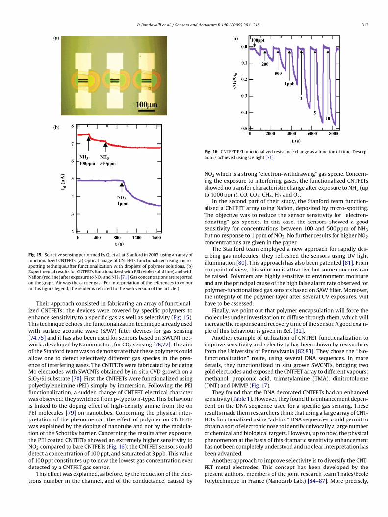
Their approach consisted in fabricating an array of functional-zed CNTFETs: the devices were covered by specific polymers tonhance sensitivity to a specific gas as well as selectivity (Fig. 15).his technique echoes the functionalization technique already usedith surface acoustic wave (SAW) filter devices for gas sensing
74,75] and it has also been used for sensors based on SWCNT net-orks developed by Nanomix Inc., for CO2 sensing [76,77]. The aim
f the Stanford team was to demonstrate that these polymers couldllow one to detect selectively different gas species in the pres-nce of interfering gases. The CNTFETs were fabricated by bridgingo electrodes with SWCNTs obtained by in-situ CVD growth on a
iO2/Si substrate [78]. First the CNTFETs were functionalized usingolyethyleneimine (PEI) simply by immersion. Following the PEIunctionalization, a sudden change of CNTFET electrical characteras observed: they switched from p-type to n-type. This behaviour
s linked to the doping effect of high-density amine from the onEI molecules [79] on nanotubes. Concerning the physical inter-retation of the phenomenon, the effect of polymer on CNTFETsas explained by the doping of nanotube and not by the modula-
ion of the Schottky barrier. Concerning the results after exposure,he PEI coated CNTFETs showed an extremely higher sensitivity toO2 compared to bare CNTFETs (Fig. 16): the CNTFET sensors could
etect a concentration of 100 ppt, and saturated at 3 ppb. This valuef 100 ppt constitutes up to now the lowest gas concentration everetected by a CNTFET gas sensor.This effect was explained, as before, by the reduction of the elec-rons number in the channel, and of the conductance, caused by
Fig. 16. CNTFET PEI functionalized resistance change as a function of time. Desorp-tion is achieved using UV light [71].
NO2 which is a strong “electron-withdrawing” gas specie. Concern-ing the exposure to interfering gases, the functionalized CNTFETsshowed no transfer characteristic change after exposure to NH3 (upto 1000 ppm), CO, CO2, CH4, H2 and O2.
In the second part of their study, the Stanford team function-alised a CNTFET array using Nafion, deposited by micro-spotting.The objective was to reduce the sensor sensitivity for “electron-donating” gas species. In this case, the sensors showed a goodsensitivity for concentrations between 100 and 500 ppm of NH3but no response to 1 ppm of NO2. No further results for higher NO2concentrations are given in the paper.
The Stanford team employed a new approach for rapidly des-orbing gas molecules: they refreshed the sensors using UV lightillumination [80]. This approach has also been patented [81]. Fromour point of view, this solution is attractive but some concerns canbe raised. Polymers are highly sensitive to environment moistureand are the principal cause of the high false alarm rate observed forpolymer-functionalized gas sensors based on SAW filter. Moreover,the integrity of the polymer layer after several UV exposures, willhave to be assessed.
Finally, we point out that polymer encapsulation will force themolecules under investigation to diffuse through them, which willincrease the response and recovery time of the sensor. A good exam-ple of this behaviour is given in Ref. [32].
Another example of utilization of CNTFET functionalization toimprove sensitivity and selectivity has been shown by researchersfrom the University of Pennsylvania [82,83]. They chose the “bio-functionalization” route, using several DNA sequences. In moredetails, they functionalized in situ grown SWCNTs, bridging twogold electrodes and exposed the CNTFET array to different vapours:methanol, propionic acid, trimetylamine (TMA), dinitrotoluene(DNT) and DMMP (Fig. 17).
They found that the DNA decorated CNTFETs had an enhancedsensitivity (Table 1). However, they found this enhancement depen-dent on the DNA sequence used for a specific gas sensing. Theseresults made them researchers think that using a large array of CNT-FETs functionalized using “ad-hoc” DNA sequences, could permit toobtain a sort of electronic nose to identify univocally a large numberof chemical and biological targets. However, up to now, the physicalphenomenon at the basis of this dramatic sensitivity enhancementhas not been completely understood and no clear interpretation has
been advanced.Another approach to improve selectivity is to diversify the CNT-FET metal electrodes. This concept has been developed by thepresent authors, members of the joint research team Thales/EcolePolytechnique in France (Nanocarb Lab.) [84–87]. More precisely,
314 P. Bondavalli et al. / Sensors and Actuators B 140 (2009) 304–318
Fig. 17. DNA SWCNT functionalization performed by Staii et al. at Pennsylvania University in 2005: AFM images and line scans of the same SWCNT before (a) and after (b)DNA functionalization [82].
Table 1Source/drain current change after exposure to different analytes for a CNTFET functionalized using two different DNA sequences [82].
Odor Vapour pressure (Torr) Estimated concentration (ppm) % �I/I
Bare swCN swCN + Seq l swCN + Seq 2
Water 17.5 700 0 ± 1 0 ± 1 0 ± 1Propionic acid 4 150 0 ± 1 +17 ± 2 +8 ± 1TMDD
wbgecg
Fic
MA 500 20000ethanol 100 4000MMP 0.6 25NT 1 40
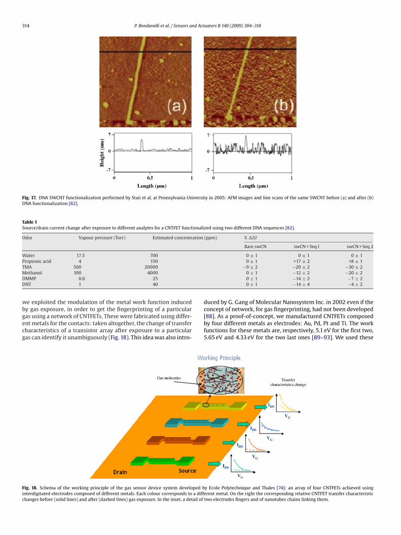
e exploited the modulation of the metal work function inducedy gas exposure, in order to get the fingerprinting of a particular
as using a network of CNTFETs. These were fabricated using differ-nt metals for the contacts: taken altogether, the change of transferharacteristics of a transistor array after exposure to a particularas can identify it unambiguously (Fig. 18). This idea was also intro-ig. 18. Schema of the working principle of the gas sensor device system developed bnterdigitated electrodes composed of different metals. Each colour corresponds to a diffhanges before (solid lines) and after (dashed lines) gas exposure. In the inset, a detail of
−9 ± 2 −20 ± 2 −30 ± 20 ± 1 −12 ± 2 −20 ± 20 ± 1 −14 ± 2 −7 ± 20 ± 1 −14 ± 4 −4 ± 2
duced by G. Gang of Molecular Nanosystem Inc. in 2002 even if theconcept of network, for gas fingerprinting, had not been developed
[88]. As a proof-of-concept, we manufactured CNTFETs composedby four different metals as electrodes: Au, Pd, Pt and Ti. The workfunctions for these metals are, respectively, 5.1 eV for the first two,5.65 eV and 4.33 eV for the two last ones [89–93]. We used thesey Ecole Polytechnique and Thales [74]: an array of four CNTFETs achieved usingerent metal. On the right the corresponding relative CNTFET transfer characteristictwo electrodes fingers and of nanotubes chains linking them.

P. Bondavalli et al. / Sensors and Actuators B 140 (2009) 304–318 315
Fig. 19. Left-hand side: SEM image of interdigited CNT transistors fabricated at Thales Reserandom network between two electrodes.
Table 2Summary of the results and number of transistors tested for each differentmetal electrode.
Current reduction after DMMP exposure
Metals IDS current reduction % after exposure(1 ppm DMMP) error ± 5%
Ti/Pd 90
mon
dttnTom
[95,96]. They exposed this array to several gases (NO [92], H2, CO,
Fu
Ti/Au 65Ti 50Ti/Pt 20
etals in order to check whether the gas interaction was relatednly to the initial work function of a metal or if it depended on theature of gas and electrode interaction.
We performed several measurements using different electrodeesigns (20 transistors for each metal with different electrodes dis-ance (Fig. 19)) and these results were in close agreement withhe initial hypothesis: it seemed that the sensor sensitivity was
ot influenced by the number of nanotubes linking the electrodes.he results obtained after exposure of CNTFET transistors to 1 ppmf DMMP in ambient conditions are shown in Table 2. From theseeasurements, researchers formulated the hypothesis that differ-ig. 20. CNTFET based sensor chip developed by Starr et al. at Nanomix Inc. [95], (a) optsing different metals. (c) SEM image of CNT with metal particles on their surfaces. (d) HR
arch and Technology in 2006 [86]. Right-hand side: AFM detail of carbon nanotubes
ent metals interact in a different way with the DMMP. The resultshowing that the Pd and Au transfer characteristic change was verydifferent is particularly interesting, since these two metals havethe same work function. This seems to confirm that the effect ofgas on CNTFET characteristics was not simply related to the initialmetal work function but probably to a specific chemical interactionbetween the metal and the gas: apparently the DMMP moleculesinfluence the metal work function in a specific way and so the elec-tric response of the transistor. New measurements are in progressto confirm these results.
Another interesting approach has been developed byresearchers at Nanomix Inc. and Pittsburgh University. Theyexploited an idea first introduced in 2001 by Kong et al. of StanfordUniversity [94]: to decorate the SWCNTs constituting the channel ofa CNTFET with metal nanoparticles. They deposited nanoparticlesof different metals on networks of SWCNTs connecting two Pdelectrodes (Fig. 20). Therefore, they fabricated an array of CNTFETseach one being characterized by a different metal “decoration”
CH4, H2S, NO2, NH3 [96]) and they observed a specific change of thetransfer characteristics of each transistor as a function of the natureof the nanoparticles and of the gas. These results made researchersthink them that large array of “metal-decorated” CNTFETs could
ical image of the sensor chip on a TO-type header. (b) Array of CNTFETs decoratedTEM image of Pd decorated CNTs.

3 nd Act
be
toHPcdes
ftt(teaac
Findvogatd
16 P. Bondavalli et al. / Sensors a
e used in order to recognize univocally any gas, identifying itslectronic fingerprinting.
Regarding the physics of the phenomenon, researchers fromhe Stanford team, who had analyzed the electrical behaviour ofne CNTFET decorated with Pd nanoparticles after exposure to2, stated that the H2 dissociated on the Pd surface lowered thed work function. This reduction gave rise to an increase of theontact Schottky barrier for holes thus reducing the channel con-uctance of the p-type device. This hypothesis could explain thexperimental results for H2 but could not be applied for other gaspecies.
Kauffman and Starr [96] failed to try an exhaustive explanationor the phenomenon but underlined the main difference betweenhe interaction of metal nanoparticles/SWCNTs and metal elec-rodes/SWCNTs. In the first case without any molecular interactionexposure to gas), the nanoparticles acted exactly as inert hole scat-ering sites, reducing mobility. Only upon molecular interaction,
lectronic interaction between NO and the metal nanoparticle cre-tes added electronic density on the metal, which after crossingsmall potential barrier results in electron-hole recombinationsreating a negative shift in the device gate voltage. In this case the
ig. 21. Measurements performed by Chang et al. at Yonsei University (South Korea)n 2007 describing the dynamic of gas desorption on CNTFET achieved using SWCNTetworks. (a) Effect of inversing the gate voltage on the gas desorption of NH3 forifferent concentrations (30 and 300 ppm). In the bottom of the picture, the gateoltage as a function of time. In the inset a detailed view of the current as a functionf the decay time: the decay rate of NH3 does not depend on the concentration of theas. (b) Effect of inversing the gate voltage on the gas desorption of NH3, benzenend ethanol. In the bottom of the picture, the gate voltage as a function of time. Inhe inset the different decay rate as a function of the gas: each gas has its specificecay rate [60].
uators B 140 (2009) 304–318
metal nanoparticle/SWCNTs junctions could be described using theYamada model, introduced previously.
A very different approach to carry out with success selectivityhas been proposed by researchers at Yonsei University in SouthKorea [60]. As quoted in the previous paragraph, they obtainedrefreshable sensors inversing the polarity of the gate voltage afterNO2 and NH3 gas exposure. Indeed, they pushed more deeplytheir analysis and observed that the rate of desorption of the gasmolecules was dependent on their nature. They observed that afterexposure to 30 and 300 ppm of NH3 and after refreshing the CNTFETbased sensor applying a gate voltage of 10 V (to accelerate gas des-orption), the slope of the IDS as a function of time (decay rate) wasthe same in both cases (−0.1 nA s−1) and was due to the concentra-tion but only to the gas type. After having exposed the same deviceto ethanol (1000 ppm) and benzene (15 ppm), they obtained, afterrefreshing at the same voltage, different decay rates: −0.07 nA s−1
for ethanol and −0.04 nA s−1 for benzene (see Fig. 21). These resultsmade them think that the decay rate could be used to perform selec-tive measurements of the gas species considering that this timeinterval is univocally related to the binding energy of the adsorbedmolecules.
6. Conclusions
In this paper we have exposed different recent studies dealingwith gas sensors based on CNTFETs, whether made with individualSWNTs or with random SWNT networks (mats). The main sens-ing mechanism seems to be the modulation of the Schottky barrierheight at the contacts, due to the build-up of interface dipoles thatdepend on the gas specie, but also on the chemical reactivity of themetal constituting the source and drain electrodes. The “wetting”of the contact metal on the nanotubes is also a parameter to takeinto account in the sensing mechanism, since it can shape the inter-face, leading to the formation of a transition region of paramountimportance.
Devices based on mats show very promising performances forstriking the sensor market in the next years. Numerous advan-tages can be advanced: extreme sensitivity (down to 100 ppt forNO2), very short response and recovery times (some seconds),good efficiency at room temperature, low power consumption,CMOS compatibility (relatively low cost). One of the major prob-lems now is to get a higher selectivity compared to other existinggas sensor technologies. Different routes to improve selectivity,have been proposed. They are based on the diversification of metalelectrodes, polymer functionalization, metal particle decorationof the SWCNT mat, time desorption resolution. Common to allthese approaches is the tendency to multiply the number of mea-surements using different sensor parameters (the metal electrodesnature, the functionalising polymers, the metal particles on the mat,. . .), in order to develop a matrix or an array of CNTFETs that willallow one to identify accurately the “signature” of a particular gas.This seems to be the most viable route to achieve highly selectivedevices.
Moreover, the theoretical efforts for an in depth understandingand modelling of the interaction of gases with CNTFETs (obtainedusing a single SWNT or a mat) must be enhanced. For example, theeffect of gases on polymer- or DNA-functionalised CNTFETs or onmetal electrodes is not yet completely clear.
Finally, other technological hurdles must be overcome in orderto bring these sensors out of research laboratories: the design andfabrication of suitable driving circuits (particularly for arrays of
CNTFETs), the stability of the sensor response during long periodsof time, the influence of humidity, etc.Last but not least, other nanomaterials such as semiconductor oroxide nanowires could also be used in the future as active materialsfor gas sensing [97].
nd Act
R
[
[
[
[
[
[
[
[
[
[
[
[
[
[
[
[
[
[
[
[
[
[
[
[
[
[
[
[
[
[
[
[
[
[
[
[
[
[
[
[
[
[
[
[
[
[
[
[
[
[
[
[
[
[
[
[
[
P. Bondavalli et al. / Sensors a
eferences
[1] S. Ijima, Helical microtubules of graphitic carbon, Nature 354 (1991) (1991)56–58.
[2] Ph. Avouris, Z. Chen, V. Perebeinos, Carbon-based electronics, Nat. Nanotechnol.2 (2007) 605–615.
[3] P.G. Collins, M. Hersam, M. Arnold, R. Martel, P. Avouris, Current saturation andelectrical breakdown in multiwalled carbon nanotubes, Phys. Rev. Lett. 86 (14)(2001) 3128–3131.
[4] P. Kim, L. Shi, A. Majumdar, P.L. McEuen, Thermal, transport measurements ofindividual multiwalled nanotubes, Phys. Rev. Lett. 87 (21) (2001) 215502.
[5] M. Fujii, X. Zhang, H. Xie, H. Ago, K. Takahashi, T. Ikuta, H. Abe, T. Shimizu,Measuring the thermal conductivity of a single wall nanotube, Phys. Rev. Lett.95 (6) (2005) 065502.
[6] J. Hone, M.C. Llaguno, M.J. Biercuk, A.T. Johnson, B. Batlogg, Z. Benes, J.E. Fischer,Thermal properties of carbon nanotubes and nanotubes-based materials, Appl.Phys. A 74 (3) (2002) 339–343.
[7] R.S. Ruoff, D. Qian, W. Kam Liu, Mechanical properties of carbon nanotubes:theoretical predictions and experimental measurements, C. R. Phys. 4 (2003)993–1008.
[8] W.A. de Heer, A. Chatelain, D. Urgate, A carbon nanotube field-emission electronsource, Science 270 (1995) 1179–1180.
[9] S. Fan, M.G. Chapline, N.R. Franklin, T.W. Tombler, A.M. Cassell, H. Dai, Self-oriented regular arrays of carbon nanotubes and their field emission properties,Science 283 (1999) 512–514.
10] L. Hudanski, E. Minoux, L. Gangloff, K.B.K. Teo, J.-P. Schnell, S. Xavier, W.I. Milne,D. Pribat, J. Robertson, P. Legagneux, Carbon nanotube based photocathode”,Nanotechnology 19 (2008) 105201.
11] K.B.K. Teo, E. Minoux, L. Hudanski, F. Peauger, J.-P. Schnell, L. Gangloff, P. Legag-neux, D. Dieumegard, G. Amaratunga, W.I. Milne, Microwave devices: carbonnanotube as cold cathodes, Nature 437 (2005) 968.
12] H. Sugie, M. Tanemura, V. Filip, K. Iwata, K. Takahashi, F. Okuyama, High-densitygrowth of vertically aligned carbon nanotubes with high linearity by catalystpreheating in acetylene atmosphere, Appl. Phys. Lett. 78 (17) (2001) 2578–2580.
13] R. Prasher, Thermal interface materials: historical perspective, status and futuredirections, Proceedings of the IEEE 94 (8) (2006) 1571–1586.
14] D. Qian, G.J. Wagner, W.K. Liu, M.-F. Yu, R.S. Ruoff, Mechanics of carbon nan-otubes, Appl. Mech. Rev. 55 (6) (2002) 495–532.
15] J. Appenzeller, J. Knoch, R. Martel, V. Derycke, S.J. Wind, Carbon nanotubeselectronics, IEEE Trans. Nanotechnol. 1 (4) (2002) 184–189.
16] H. Dai, Carbon nanotubes: opportunities and challenges, Surf. Sci. 500 (2002)218–241.
17] N. Sinha, J. Ma, J.T.W. Yeow, Carbon nanotube-based sensors, J. Nanosci. Nan-otechnol. 6 (2006) 573–590.
18] R.J. Chen, H.C. Choi, S. Bangsaruntip, E. Yenilmez, X. Tang, Q. Wang, Y.-L. Chang,H. Dai, An investigation of the mechanisms of electronic sensing of proteinadsorption on carbon nanotube devices, J. Am. Chem. Soc. 26 (5) (2004) 1563–1568.
19] R.J. Chen, S. Bangsaruntip, K.A. Drouvalakis, N.W.S. Kam, M. Shim, Y. Li, W. Kim,P.J. Utz, H. Dai, Carbon nanotubes as biocompatible materials and highly specificelectronic biosensors, Proc. Natl. Acad. Sci. U.S.A. 100 (2003) 4984–4989.
20] N. Koratkar, P. Ajayna, A. Modi, E. Lass, Miniaturized gas sensors featur-ing electrical breakdown in the vicinity of carbon nanotubes tips, PatentWO/2004/059298.
21] A. Goldoni, L. Petaccia, S. Lizzit, R. Larciprete, Interaction of Single-walled carbonnanotubes with gases: sample contaminants and environmental monitoring,in: Proceeding of the 3rd Stig Lundqvist Conference on Advancing Frontiers ofCondensed Matter Physics, Trieste (Italy), August 11–15, 2003.
22] T. Ueda, H. Norimatsu, Md.M.H. Bhuiyan, T. Ikegami, K. Ebihara, NO sensingproperty of carbon nanotube based thin film gas sensors prepared by chemicalvapor deposition techniques, Jpn. J. Appl. Phys. 45 (10B) (2006) 8393–8397.
23] J. Li, Y. Lu, Q. Ye, M. Cinke, J. Han, M. Meyyappan, Carbon nanotube sensors forgas and organic vapor detection, Nanoletters 3 (7) (2003) 929–933.
24] L. Valentini, I. Armetano, J.H. Kenny, C. Cantalini, L. Lozzi, S. Santucci, Sensorsfor sub-ppm NO2 gas detection based on carbon nanotube thin film, Appl. Phys.Lett. 82 (6) (2003) 961–963.
25] R. Saito, G. Dresselhaus, M.S. Dressealhaus, Physical properties of carbon nan-otubes, Imperial College Press, London, 1998, p. 259.
26] J. Kong, N. Franklin, C. Chou, S. Pan, K.J. Cho, H. Dai, Nanotube molecular wiresas chemical sensors, Science 287 (2000) 622–625.
27] C.W. Bauschlicher, A. Ricca, Binding of NH3 to graphite and to (9,0) carbonnanotubes, Phys. Rev. B 70 (2004) 115409.
28] J. Zhao, A. Buldum, J. Han, J. Ping Lu, Gas molecule adsorption in carbon nan-otubes and nanotube bundles, Nanotechnology 13 (2002) 195–200.
29] J. Zhao, A. Buldum, J. Han, J. Ping Lu, Gas molecules adsorption on carbon nan-otubes, Mater. Res. Soc. Proc. 633 (2001), 3.48.1-A13.48.6.
30] S. Peng, K. Cho, Chemical control of nanotube electronics, Nanotechnology 11(2000) 57–60.
31] X. Liu, Z. Luo, S. Han, T. Tang, D. Zhang, C. Zhou, Band engineering of carbonnanotube field-effect transistors via selected area chemical gating, Appl. Phys.
Lett. 86 (2005) 243501.32] J. Zhang, A. Boyd, A. Tselev, M. Paranjape, P. Barbara, Mechanism of NO2 detec-tion in carbon nanotube field effect transistor chemical sensors, Appl. Phys. Lett.88 (2006) 123112.
33] V. Derycke, R. Martel, J. Appenzeller, Ph. Avouris, Controlling doping and carrierinjection in carbon nanotubes transistors, Appl. Phys. Lett. 80 (15) (2002) 2773.
[
[
uators B 140 (2009) 304–318 317
34] S. Heinze, J. Tersoff, R. Martel, V. Derycke, J. Appenzeller, Ph. Avouris, Carbonnanotubes as Schottky barrier transistors, Phys. Rev. Lett. 89 (10) (2002) 106801.
35] S. Heinze, J. Tersoff, P. Avouris, Electrostatic engineering of nanotube transistorsfor improved performance, Appl. Phys. Lett. 83 (24) (2003) 5038–5040.
36] X. Cui, M. Freitag, R. Martel, L. Brus, Ph. Avouris, Controlling energy-level align-ment at carbon nanotubes/Au contact, Nanoletters 3 (6) (2003) 783–787.
37] F. Leonard, J. Tersoff, Role of Fermi-level pinning in nanotubes Schottky diodes,Phys. Rev. Lett. 84 (20) (2000) 4693.
38] S. Auvray, J. Borghetti, M.F. Goffman, A. Filoramo, V. Derycke, J.P. Bourgoin, Car-bon nanotubes transistor optimization by chemical control of nanotubes-metalinterface, Appl. Phys. Lett. 84 (25) (2005) 5106.
39] X. Crispin, M. Geskin, A. Crispin, J. Cornil, R. Lazzaroni, W.R. Salaneck, J.L. Bredas,J. Am. Chem. Soc. 124 (2002) 8131–8141.
40] X. Crispin, Interface dipole at organic/metal interfaces and organic solar cells,Sol. Energy Mater. Sol. Cells 83 (2–3) (2004) 147–168.
41] T. Yamada, Modeling of carbon nanotubes Schottky barrier modulation underoxidizing conditions, Phys. Rev. B 69 (2004) 125408.
42] T. Yamada, Equivalent circuit model for carbon nanotubes Schottky barrier:Influence of neutral polarized gas molecules, Appl. Phys. Lett. 88 (2006) 083106.
43] H. Dai, A. Javey, E. Pop, D. Mann, Y. Lu, Electrical transport properties and field-effect transistors of carbon nanotubes, NANO 1 (1) (2006) 1–4.
44] W. Kim, A. Javey, O. Vermesh, Q. Wang, Y. Li, H. Dai, Hysteresis caused bywater molecules in carbon nanotube field-effect transistors, Nano Lett. 3 (2003)193–198.
45] D. Sung, S. Hong, Y.-H. Kim, Ab initio study of the effect of water adsorption onthe carbon nanotube field-effect transistor, Appl. Phys. Lett. 89 (2006) 243110.
46] P. Na, H. Kim, H.M. So, K.J. Kong, H. Chang, B. Ryu, Y. Choi, J.O. Lee, B.K. Kim, J.J.Kim, J. Kim, Investigation of the humidity effect on the electrical properties ofsingle-walled carbon nanotube transistors, Appl. Phys. Lett. 87 (2005) 093101.
47] A. Zahab, L. Spina, P. Poncharal, C. Marlière, Water-vapor effect on the electricalconductivity of a single-walled carbon nanotube mat, Phys. Rev. B 62 (2000)10000–10003.
48] R.S. Mulliken, Electronic population analysis on LCAO-MO molecular wave func-tions, J. Chem. Phys. 23 (10) (1955) 1833–1840.
49] S.A. Mc Gill, S.G. Rao, P. Manadhar, P. Xiong, S. Hong, High-performances,hysteresis-free carbon nanotube field-effect transistors via directed assembly,Appl. Phys. Lett. 89 (2006) 163123.
50] S. Kar, A. Vijayaraghavan, C. Soldano, S. Talapatra, Quantitative analysis of hys-teresis in carbon nanotube field-effect devices, Appl. Phys. Lett. 89 (13) (2006)132118.
51] M. Rinkiö, M.Y. Zavodchikova, P. Törmä, A. Johansson, Effect of humidity on thehysteresis of single walled carbon nanotube field-effect transistors, Phys. StatusSolidi (b) 245 (2008) 2315–2318.
52] S. Kumar, G.B. Blanchet, M. Hybertsten, J.Y. Murthy, M.A. Alam, Performanceof carbon nanotube-dispersed thin-film transistors, Appl. Phys. Lett. 89 (2006)143501.
53] S. Kumar, J.Y. Murthy, M.A. Alam, Percolating conduction in finite nanotubenetworks, Phys. Rev. Lett. 95 (2005) 066802.
54] E.S. Snow, J.P. Novak, P.M. Campbell, D. Park, Random networks of carbon nan-otubes as an electronic material, Appl. Phys. Lett. 82 (13) (2003) 2145.
55] S. Kumar, N. Pimparkar, J.Y. Murthy, A.A. Alam, Theory of transfer characteristicsof nanotube networks transistors, Appl. Phys. Lett. 88 (12) (2006) 123505.
56] E. Berkyarova, M.E. Itkis, N. Cabrera, B. Zhao, A. Yu, J. Gao, R.C. Haddon, Electronicproperties of single-walled carbon nanotube networks, J. Am. Chem. Soc. 127(16) (2005) 5990–5995.
57] J.P. Novak, E.S. Snow, E.J. Houser, D. Park, J.L. Stepnowski, R.A. McGill, Nerveagent detection using networks of single-walled carbon nanotubes, Appl. Phys.Lett. 83 (19) (2003) 4026–4029.
58] E.S. Snow, F.K. Perkins, J.A. Robinson, Chemical vapour detection using single-walled carbon nanotubes, Chem. Soc. Rev. 35 (2006) 790–798.
59] A.R. Hopkins, N.S. Lewis, Detection and classification characteristics of arraysof carbon black/organic polymer composite chemiresistive vapor detectorsfor the nerve agent simulants dimethylmethylphosphonate and diisopropyl-methylphosponate, Anal. Chem. 73 (2001) 884–892.
60] Y.W. Chang, J.S. Oh, S.H. Yoo, H.H. Choi, K.-H. Yoo, Electrically refreshable carbon-nanotube-based gas sensors, Nanotechnology 18 (2007) 435504.
61] S.Y. Jeong, K.K. Kim, K.H. Kim, H.R. Hwang, C.S. Han, M.H. Yun, Nano: Brief Rep.Rev. 1 (3) (2006) 235–241.
62] J. Kong, H. Dai, Full and modulated chemical gating of individual carbon nan-otubes by organic amine compounds, J. Phys. Chem. 105 (2001) 2890–2893.
63] J. Kong, H. Soh, A. Cassel, C.F. Quatec, H. Dai, Synthesis of individual singlewalledcarbon nanotubes on patterned siliconwafers, Nature 395 (1998) 878–879.
64] F.E. Jones, A.A. Talin, F. Leonard, P.M. Dentinger, W.M. Clift, Effect of electrodesmaterial on transport and chemical sensing characteristics of metal/carbonnanotubes, J. Electron. Mater. 35 (8) (2006) 1641–1646.
65] J. Dieng, K. Ghosh, H.S.P. Wong, Modeling Carbon Nanotube Sensors, IEEE Sens.J. 7 (9) (2007) 1356–1357.
66] J. Li, Y. Lu, Q. Ye, L. Delzeit, M. Meyappan, A gas sensor array using carbon nan-otubes and microfabrication technology, Electrochem. Solid-state Lett. 8 (11)(2005) H100–102.
67] L. Delzeit, B. Chen, A.M. Cassel, R. Stevens, C. Nguyen, M. Meyyappan, Mul-tilayered metal catalysts for controlling the density of single-walled carbonnanotube growth, Chem. Phys. Lett. 348 (2001) 368–374.
68] M.S. Fuhrer, J. Nygård, L. Shih, M. Forero, Y.-G. Yoon, M.S.C. Mazzoni, H.J Choi, J.Ihm, S.G. Louie, A. Zettl, P.L. McEuen, Crossed nanotube junctions, Science 288(2000) 494.

3 nd Act
[
[
[
[
[
[
[
[
[
[
[
[
[[
[
[
[
[
[
[
[
[
[
[
[
[
[
[
[
18 P. Bondavalli et al. / Sensors a
69] B. Gao, Y.F. Chen, M.S. Fuhrer, D.C. Glattli, A. Bachtold, Four-point resistance ofindividual single-wall carbon nanotubes, Phys. Rev. Lett. 95 (2005) 196802.
70] P.L. McEuen, J. Park, A. Bachtold, M. Woodside, M.S. Fuhrer, M. Bockrath, L. Shi, A.Majumdar, P. Kim, Nanotube Nanoelectronics, in: Device Research ConferenceDigest, IEEE, Piscataway, NJ, USA, 2001.
71] P. Qi, O. Vermesh, M. Grecu, A. Javey, Q. Wang, H. Dai, S. Peng, K.J. Cho, Towardslarge arrays of multiplex functionalized carbon nanotube sensors for highlysensitive and selective molecular detection, Nano Lett. 3 (2003) 347–351.
72] E.S. Snow, F.K. Perkins, Capacitance and conductance of single-walled car-bon nanotubes in the presence of chemical vapors, Nano Lett. 5 (12) (2005)2414–2417.
73] J.A. Robinson, E.S. Snow, S.C. Badescu, T.L. Reinecke, F.K. Perkins, Role of defectsin single-walled carbon nanotubes chemical sensor, Nano Lett. 6 (8) (2006)1747–1751.
74] M.S. Niewenhuizen, J.L.N. Harteveld, Studies on a surface acoustic wave (SAW)dosimeter sensor for organophosphorous nerve agents, Sens. Actuators B 40(1997) 167–173.
75] D. Williams, G. Pappas, Rapid identification of nerve agents Sarin (GB) andSoman (GD) with the use of a field-portable GC/SAW vapor detector and liquiddesorption front-end device, Field Anal. Chem. Tech. 3 (1999) 45–53.
76] A. Star, V. Joshi, D. Thomas, J. Niemann, J.-C.P. Gabriel, C. Valcke, NanoelectronicCO2 breath sensors, in: Technical Proceedings of the 2005 NSTI Nanotechnology,Anaheim, CA, USA, May 8–12, 2005.
77] A. Star, T.-R. Han, V. Joshi, J.-C.P. Gabriel, G. Grüner, Nanoelectronic carbondioxide sensors, Adv. Mater. 16 (2004) 2049–2052.
78] N.R. Franklin, Q. Wang, T.W. Tombler, A. Javey, M. Shim, H. Dai, Integration of sus-pended carbon nanotube arrays into electronic devices and electromechanicalsystems, Appl. Phys. Lett. 81 (2002) 913–915.
79] M. Shim, A. Javey, N.W.S. Kam, H. Dai, Polymer functionalization for air-stablen-type carbon nanotube field-effect transistors, J. Am. Chem. Soc. 123 (2001)11512–11513.
80] R. Chen, N.R. Franklin, J. Kong, J. Cao, T.W. Tombler, T. Zhang, H. Dai, Molecularphotodesorption from single-walled carbon nanotubes, Appl. Phys. Lett. 79 (14)(2001) 2258–2260.
81] H. Dai, R.J. Chen, Photodesorpion in Carbon Nanotubes, Patent WO 02/086480.82] C. Staii, A.T. Johnson, M. Chen, A. Gelperin, DNA-decorated carbon nanotubes
for chemical sensing, Nano Lett. 5 (9) (2005) 1774–1778.83] A.T. Johnson, C. Staii, M. Chen, S. Khamis, R. Johnson, M.L. Klein, A. Gelperin,
DNA-decorated carbon nanotubes for chemical sensing, Semicond. Sci. Technol.21 (2006) S17–21.
84] P. Bondavalli, P. Legagneux, D. Pribat, P. Lebarny, J. Naigle, Conductive nanotubeor nanowires FET transistor network and corresponding device, for detectinganalytes, Patent WO2006128828.
85] P. Bondavalli, P. Legagneux, D. Pribat, Gas fingerprinting using carbonnanotubes, transistor array, in: Technical Proceedings of the 2007 NSTI Nan-otechnology Conference and Trade Show, vol. 3, 2007, pp. 29–32.
86] P. Bondavalli, P. Legagneux, D. Pribat, Capteurs de gaz à base de transistors ànanotubes de carbone: une nouvelle génération de capteurs manométriques,REE 4 (2007) 1–13.
87] P. Bondavalli, P. Legagneux, D. Pribat, Gas fingerprinting using carbon nanotubestransistors arrays, J. Exp. Nanosci. 3 (04) (2008) 347–356.
88] G. Gang, L. S. Pan, Nanotube chemical sensor based on work function of elec-
trodes, Patent WO2004051219.89] Y. Morikawa, H. Ihii, K. Seki, Theoretical study of n-alkane adsorption on metalsurfaces, Phys. Rev. B 69 (2004) 041403.
90] T. Mori, T. Kozawa, T. Ohwaki, Y. Taga, S. Nagai, S. Yamasaki, S. Asami, N. Shibata,M. Koike, Schottky barriers and contact resistances on p-type GaN, Appl. Phys.Lett. 69 (23) (1996) 3537–3539.
uators B 140 (2009) 304–318
91] J. Hölzl, F.K. Schulte, in: G. Hoehler (Ed.), Springer Tracts in Modern Physics, vol.1, Springer-Verlag, Berlin, 1977, p. 1.
92] M.H. Yang, K.B.K. Teo, W.I. Milne, D.G. Hasko, Carbon nanotube Schottky diodeand directionally dependent field-effect transistor using asymmetrical con-tacts, Appl. Phys. Lett. 87 (25) (2005) 253116.
93] K. Kang Kim, D. Jae Bae, C.-M. Yang, K.H. An, J.Y. Lee, Y.H. Lee, J. Nanosci. Nan-otechnol. 5 (2005) 1055–1059.
94] J. Kong, G. Michael, G. Chapline, H. Dai, Functionalized carbon nanotubes formolecular sensors, Adv. Mater. 13 (18) (2001) 1384–1386.
95] A. Starr, V. Joshi, S. Skarupo, D. Thomas, J-C.P. Gabriel, Gas sensor array based onmetal-decorated carbon nanotubes, J. Phys. Chem. B 110 (2006) 21014–21020.
96] D.R. Kauffmann, A. Starr, Chemically induced potential barriers at carbonnanotube-metal nanoparticle interface, Nano Lett. 7 (7) (2007) 1863–1868.
97] P.-C. Chen, F.N. Ishikawa, H.-K. Chang, K. Ryu, C. Zhou, A nanoelectronic nose:a hybrid nanowire/carbon nanotube sensor array with integrated microma-chined hotplates for sensitive gas discrimination, Nanotechnology 20 (2009)125503.
Biographies
Paolo Bondavalli was awarded his PhD from the National Institute of Applied Sci-ences of Lyon in 2000. His thesis dealt with MicroOptoMechanical Systems (MOEMS)for gas sensing. The same year, he joined Thales Laser Diodes (TLD) research anddevelopment team where he worked on developing micropackaging and test facil-ities for power laser diodes. He moved to Thales Research and Technology (TRT) in2001 where he joined the MEMS Microtech team. He was in charge of the micropack-aging design of MEMS RF devices. He joined the NANOCARB Laboratory in TRT during2004. His research deals with carbon nanotubes gas sensor, Silicon nanowires basedsensors for biological detection, thermal management using CNT. He is the authorand coauthor of 20 scientific papers dealing with MOEMS, MEMS RF, CNTFET basedsensors and of several patents dealing with gas sensors and thermal managementthrough CNTs. He is EC expert in FP7 framework, and National French Agency expert.
Pierre Legagneux was awarded his PhD from the University of Orsay in 1989and joined the Central Research Laboratory of Thomson CSF which is now ThalesResearch & Technology. His research interests include the design and fabrication ofnanotube and nanowire based devices for electronic applications. He was the coor-dinator of two European projects which relate to the study of nanotube for fieldemission applications (Nanolith and Canvad). P. Legagneux is the author/co-authorof more than 60 papers and 15 patents including 6 on nanotube based devices. Heis the head of Nanostructures Laboratory at Thales R&T.
Didier Pribat graduated from Grenoble University in 1977. He worked for 23 yearswithin the Central Research Laboratory of Thomson-CSF (now Thales Research &Technology) on various subjects of materials science and semiconductor technolo-gies (heteroepitaxy, solid electrolytes, III–V materials and devices, . . .). In 1991 hestarted a group on Large Area Electronics and has been particularly involved in lowtemperature polysilicon technology, including polysilicon synthesis by excimer lasercrystallisation, thin film transistors (TFT) fabrication, characterisation and mod-
elling, as well as circuit design and simulation. He joined CNRS/Ecole Polytechniquein 2001 and started the activity on carbon nanotubes for molecular electronics. Heis currently Director of the Technology Transfer Office of Ecole Polytechnique andexpert to the EC and the EPSRC (London). D. Pribat has published or presented morethan 150 papers. He is also co-author of two book chapters and author or co-authorof more than 50 patents.