Sensor Alert (TechVision) - Home - Frost & Sullivan ... · PDF fileSensor Alert (TechVision)...
16
Image Sensors Image sensors will further impact the consumer, automotive, and other industries D727-TV April 08, 2016 Sensor Alert (TechVision)
Transcript of Sensor Alert (TechVision) - Home - Frost & Sullivan ... · PDF fileSensor Alert (TechVision)...

Image Sensors Image sensors will further impact the consumer, automotive, and other
industries
D727-TV
April 08, 2016
Sensor Alert
(TechVision)

2 D727-TV
Contents
Topic Slide No.
Innovations in Image Sensor 3
Fastree 3D SA–3D vision System 4
CMOSIS–CMOS Image Sensor 5
ON Semiconductor–Global Shutter CMOS Image Sensor 6
Unispectral–Hyperspectral Imaging Sensor 7
Strategic Insights 8
Key Patents and Industry Interactions 11

3 D727-TV
Innovations in Imaging

4 D727-TV
Various types of three-dimensional (3D) imaging sensors are
available in the market. In such sensors, very few light pulses are
emitted by the imaging system before the emitted pulse is
measured and received. Such sensors can have limitations in
measurement distance and acquisition speed. In particular, for
objects at a distance, the acquisition speed can be limited.
Unmet Needs Technology Profile
Who
Fastree3D aims at addressing the
growing global market needs for 3D
imaging applications. This focus has
helped the company in tracking the
needs of its customers, thereby
addressing the issues faced by the
clients.
Where
Fastree3D is a a Switzerland-
based company located in
the campus of École
polytechnique fédérale de
Lausanne Innovation Park
What
Fastree3D has developed a laser-based 3D vision
system based on a unique photo sensor platform that
uses a single photon detector. Data is derived from
both hardware and software to provide the
unambiguous and precise identification of a objects
moving at a very high speed at a long distance.
Innovation Attributes
The image sensor is
implemented with a photo
counter, which is capable of
counting to10 picoseconds. It
provides resolution of more
than 1.5 mm.
The speed and accuracy
provides 10 times better
illumination and consumes 10
times less power than other
systems.
The software part of the 3D vision
system comprises a
programmable control logic
interface module. The 3D vision
system supports different types of
operating system such as
Windows, Linux, and OSX.
Potential Applications
• Machine vision
• Driving assistance
• Gesture recognition
• Personal service robots
• Metrology
• Autonomous driving
The main features of Fastree3D vision
system are high frame rate, low light
imaging, programmable region of
interest, flexible pixel binning with
individual pixel readout, programmable
control of gain, frame rate and
exposure, and selective exclusion of
hot pixels.
Strategy
Licensing is one of the key revenue
strategies of Fastree3D. The
company has plans to license the
subsystem of its technology to
major OEMs, original design
manufacturers (ODMs), and global
Tier 1 and 2 manufacturers in
consumer electronics and
automotive industry.
3D Vision System Fastree 3D SA, Switzerland

5 D727-TV
Unmet Needs
Innovation Attributes
Potential Applications Commercialization
Strategy
The CSI2100 2 M Pixel CMOS image sensor is
expected to be commercialized by one to two
years. CMOSIS improved the CMOS image
sensor technology, including its performance in
low light conditions and enhanced sensitivity of
very small pixels.
The measurement of the phase difference between outgoing and
incoming light requires multiple pixel detectors. This further leads
to slower analog readout and digital conversion. In addition,
transit time through the detectors is such that modulations higher
than 50 MHz are not possible.
• Machine vision
• High frame rate image capture
• Inspection systems
• Endoscopy
• X-ray imaging
• Scientific instruments
• Smart sensors and system on chip
(SoC) imagers
The CMOS image sensor can operate in a 10 bit
mode and come with 12 micrometer-sized black and
white global shutter pixels.
At a high speed, the sensor works with full capacity
to detect small variations in signal
The efficient global shutter has low spatial and
temporal noise. In single exposure, it has high linear
dynamic range
Participation
CMOSIS has been one of the participants in European Commission FP7
CAReIOCA project started around 2012 and completed in 2015. The
project focuses on full-field optical coherence tomography to provide fast
cancer assessment at cellular scale with the help of novel non-invasive
optical imaging . In addition, CMOSIS is also one of the participants in
European Commission’s Horizon 2020 (H2020) program, Eyes of Things
project to develop a computer vision platform for complex artifacts and
applications such as wearables, robotics, home products, and
surveillance.
Acquisition
CMOSIS has been acquired
by AMS and is a member of
the AMS group. The
acquisition helps AMS to
expand its optical sensor
portfolio in machine vision,
medical, photographic, and
scientific imaging and many
more applications.
Technology Profile
What
Where Who
CMOSIS has developed CSI2100 2 M Pixel CMOS image
sensor and displayed the sensor in the 2015 International
Technical Show in Yokohama, Japan under the medical
imaging category. The hardware kit of the sensor is co-
developed with Pleora Technologies. The sensor employs
Pleora’s iPORT NTx-U3 Embedded Video Interface.
CMOSIS is
headquartered in
Belgium and has
offices in USA,
Portugal, and Germany
CMOSIS develops customized and
standard CMOS image sensor. The
company provides global and rolling
shutter image sensors.
CMOS Image Sensor CMOSIS, Belgium

6 D727-TV
Technology Profile
On Semiconductor is one of the
leading suppliers for semiconductor-
based solutions. The company’s
product portfolio comprises SoCs,
sensors, power management
devices, analog devices, logic
devices, and connectivity devices.
The AR0135 CMOS image sensor is developed with the global
shutter pixel design and allows effective synchronization with
pulsed light sources. This new design will help to provide clear
images with low noise in environments such as high temperature,
bright scenes, and low light.
On Semiconductor
has its
headquarters in
USA and has
offices across the
globe
Who
What Where
Innovation Attributes
The AR0135 sensor comprises a dedicated trigger and flash pins, which are
further used to synchronize multiple sensors for stereo camera applications and
control external LED light source.
The AR0135 sensor is a 1280 x 960 resolution device with 720p at 60fps and
54fps per second at full resolution.
The AR0135 sensor with the innovative global shutter pixel design, operates
with 10 times lower dark current and 4 times higher shutter efficiency than
previous generations of product. In addition, this helps the sensor to improve
the performance in gesture recognition and eye tracking functionality.
Potential Applications
Automotive imaging
High speed barcode scanning
Virtual reality
3D depth sensing
Market Opportunity
The market has a need for clear, accurate, and
high-speed imaging solutions. The global
shutter pixels from On Semiconductor provide
reliable operations in harsh environments and
resolve the challenges in high speed barcode
scanning and driver monitoring.
Commercialization Strategy
Engineering samples of the CMOS image
sensor are available and such sensors are
slated for production in the third quarter of
2016.
Global Shutter CMOS Image Sensor On Semiconductor, USA

7 D727-TV
Technology Profile
Unispectral is a startup
company and a spin off from
Tel Aviv University
Unispectral has developed a compact image
sensor based on hyperspectral imaging (which
takes images at many close-interval
wavelength bands to provide a more complete
spectrum for each pixel). Unispectral is aiming
to transform the standard of color sensing
mechanisms in compact cameras and to
provide high low-light sensitivity, rich color,
better resolution.
Unispectral is
based in Israel.
Who
What
Where
Innovation Attributes
Researchers at the company are developing a small optical component
with the help of MEMS (micro-electromechanical system) technology.
The system will identify electromagnetic fingerprints and extract vital
information from the images of various substances and processes. For
instance, just by taking a picture of a structure, the chemical composition
of the structure inside the picture can be studied by the user.
The technology will enable capturing images with rich color and better
resolution even in low light conditions.
Potential Applications
Consumer electronics
Wearable
Medical imaging
Industrial
Agriculture
Internet of Things
Funding
The company has raised $7.5 million through
Series A funding led by Jerusalem Venture
Partners, Robert Bosch Venture Capital, Samsung
Catalyst Fund, and Tel Aviv University Innovation
Momentum Fund
Commercialization Strategy
The technology is currently under development by Tel
Aviv University’s technology transfer company,
Ramot. The technology is expected to be
commercialized over the near-term.
Software will be employed to support the process in extracting the
information from the image with the help of an image fusion library
Hyperspectral Imaging Sensor Unispectral, Israel

8 D727-TV
Strategic Insights
9 D727-TV
Strategic Insights
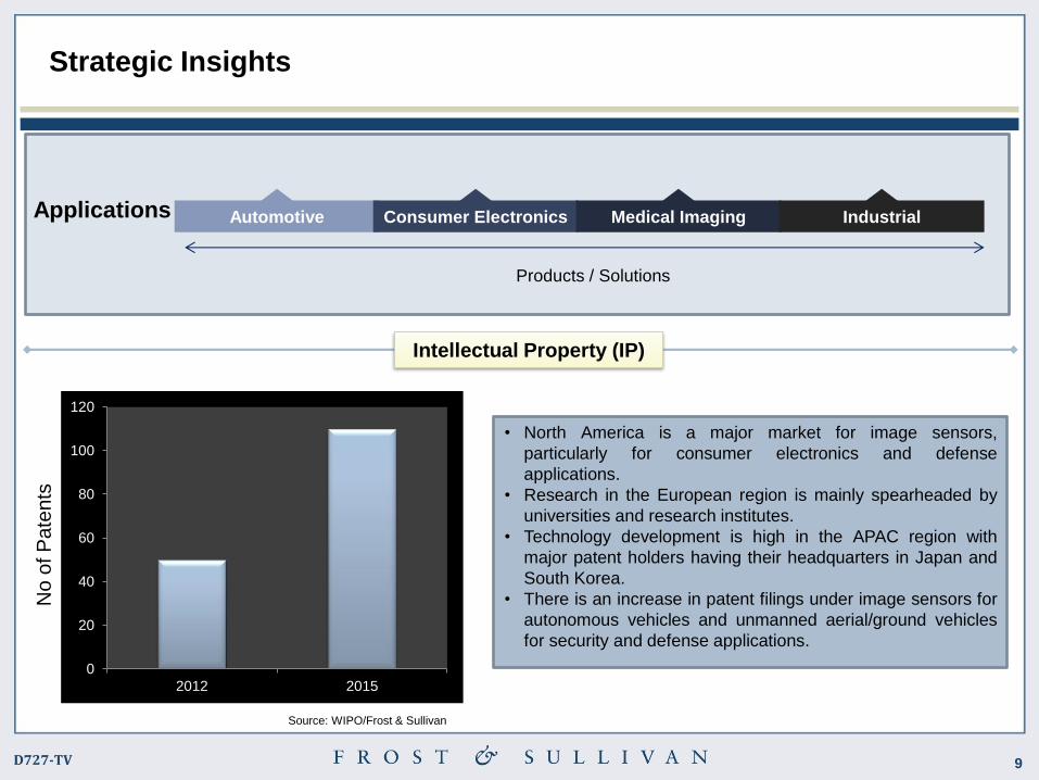
Applications Automotive Consumer Electronics Medical Imaging Industrial
• North America is a major market for image sensors,
particularly for consumer electronics and defense
applications.
• Research in the European region is mainly spearheaded by
universities and research institutes.
• Technology development is high in the APAC region with
major patent holders having their headquarters in Japan and
South Korea.
• There is an increase in patent filings under image sensors for
autonomous vehicles and unmanned aerial/ground vehicles
for security and defense applications.
Intellectual Property (IP)
No
of P
ate
nts
Source: WIPO/Frost & Sullivan
Products / Solutions
0
20
40
60
80
100
120
2012 2015

10 D727-TV
Strategic Insights (continued)
Drivers Restraints
Smartphones and tablets, as
well as automotive, will continue
to be major drivers for the
growth of CMOS image
sensors. Security is another key
application for image sensors.
Wider adoption in emerging
applications such as healthcare
(medical imaging),industrial
automation is expected to drive
growth in the medium- and
long-term
Ẋ The demands and
requirements of the
automotive industry (for
driver assistance
applications) put pressure
on sensor suppliers
Ẋ End-user consolidation
restricts opportunities for
image sensors
Ẋ Competition leads to pricing
pressures
o Occipital (USA), a provider of the structure sensor
and software for augmented reality, received
funding of around $1.3 million on Kickstarter. The
company has developed a 3D image sensor that
can be used on mobile devices, such as iPads.
o Funding support by governments and venture
capitalists is expected to accelerate the
commercialization of devices in such areas as
consumer electronics.
Funding
The 2020 Scenario
Image sensors with 3D vision will enable robots to
have better perception of their surroundings. This will
lead to humans and robots sharing the work floor and
performing tasks in unstructured environments.
The market share for image sensors in the
automotive industry will increase as cameras
become key components for increasing car safety,
driving assistance, and driving comfort. Assistance in
blind-spot viewing, lane-departure warning systems,
and automatic headlight dimming are some of the
applications for imaging in automobiles.
3D depth sensors based on time-of-flight will find
opportunities in gesture control in consumer
electronics, automotive, and so on.
Focus Areas
o Noncontact 3D laser scanners
o LIDAR
o Stereovision
o Interferometry
o Mapping large areas
o 3D machine vision
o 3D depth sensing

11 D727-TV
Key Patents

12 D727-TV
Key Patents
No. Patent No. Publication Date Title Assignee
1 US20160092714 31.03.2016 Fully-addressable sensor array for acoustic imaging
systems
Apple Inc.
An acoustic imaging system can contain a plurality of individual acoustic elements that each contain an acoustic transducer, drive circuitry,
and low voltage sense and/or read circuitry. In many embodiments both the drive circuitry and the read circuitry can be independently
addressable. For example, if the individual acoustic elements are arranged into rows and columns, each acoustic element can include
row/column drive circuit enable switches and row/column read circuit enable switches.
2 US20160093654 11.02.2016 Image sensor and method for operating the same SK hynix Inc.
An image sensor includes a photoelectric conversion element suitable for generating photocharges corresponding to incident light, a
transfer transistor suitable for transferring the generated photocharges to a floating diffusion node based on a transfer signal, and a reset
transistor suitable for resetting the floating diffusion node based on a reset signal and including a memory gate.

13 D727-TV
Key Patents (continued)
No. Patent No. Publication Date Title Assignee
3 US20160093656 31.03.2016 Image sensor device and method of manufacturing the
same
Semiconductor
Manufacturing
International (Shanghai)
Corporation
An image sensor device includes a top substrate and a subassembly. The top substrate includes a plurality of connection pillars, and the
subassembly includes a plurality of connection pads. The connection pillars on the top substrate are bonded to the connection pads in the
subassembly. The connection pillars are formed of a first metal and the connection pads are formed of a second metal.
4 US20160093658 31.03.2016 Image-sensor structures VisEra Technologies
Company Limited
An image-sensor structure is provided. The image-sensor structure includes a substrate, a plurality of photoelectric conversion units formed in
the substrate, a plurality of separated color filters formed above the substrate and the photoelectric conversion units, a first light shielding layer
surrounding the separated color filters, and a first conductive polymer element blended with a low-refractive-index component filled between
the individual separated color filters and between the all separated color filters and the first light shielding layer, wherein the first conductive
polymer element is electrically connected to a grounding pad.

14 D727-TV
Key Patents (continued)
No. Patent No. Publication Date Title Assignee
5 US20160093664 31.03.2016 Image sensor pixel cell with non-destructive readout Omnivision
Technologies Inc.
A pixel cell includes a photodiode coupled to photogenerate image charge in response to incident light. A deep trench isolation structure is
disposed proximate to the photodiode to provide a capacitive coupling to the photodiode through the deep trench isolation structure. An
amplifier transistor is coupled to the deep trench isolation structure to generate amplified image data in response to the image charge read out
from the photodiode through the capacitive coupling provided by the deep trench isolation structure. A row select transistor is coupled to an
output of the amplifier transistor to selectively output the amplified image data to a column bitline coupled to the row select transistor.

15 D727-TV
Industry Contacts

16 D727-TV
Industry Contacts
Contact
Name and
Designation
Company/
University
Address
Phone E-mail URL
Claude Florin,
CEO
Fastree 3D SA EPFL Innovation Park
Ch. de la Raye, 13.
CH-1024 Ecublens,
Switzerland.
+41223661000 [email protected] http://www.fastree3d.com/
Guy Meynants,
VP, R&D
CMOSIS Coveliersstraat 15,
B-2600 Antwerp,
Belgium
+32-3260-17-36 [email protected] http://www.cmosis.com/
Ross Jatou,
VP, Automotive
Scanning and
Imaging Division
ON
Semiconductor
5005 East McDowell
Road,
Phoenix, AZ 85008
602-819-6683 [email protected] http://www.onsemi.com
Shlomo Nimrodi,
CEO
RAMOT, Tel
Aviv University
PO Box 39296,
Tel-Aviv 61392,
Israel
+972-3-6406608 [email protected] http://www.ramot.org