Semiconductor Switching Devices. .Future Trends
15
Defence Science Journal, Vo148, No I, January 1998, pp. 45-59 (Q 1998, DESIDOC Semiconductor Switching Devices. .Future Trends s. Ahmad Central Electronics Engineering Research Institute, Pilani-333 031 ABSTRACT A variety of semiconductor devices and circuits have been successfully developed using conduction properties of electrons and holes in a number of elemental and compound semiconductors. Carriers confinement in a potential well, formed out of a thin layer of lower band gap material sandwitched between two layers of a higher band gap material, has been extended from one to two and three dimensions. Resultant oftwo-dimensional carrier sheet, quantum wire and quantum dot having discrete energy levels arising out of quantisation are being presently explored for possible device applications. A number of devices have been fabricated using resonanttunneling acrossa thin potential barrier. This has opened up several newer possibilities of using such structures for various electronic and optoelectronic devices and circuits applications as tunneling is relatively faster than conduction process. While looking into the interband tunneling between two quantum dots, possibility of a single electron switching has also been examined carefully. The idea of a single electron switching is conceptually being extended from quantl,lmdots to molecules and atoms ultimately. Simulations based on transmission of electrons through a chain of molecules and atoms have shown that tens of THz speedand functional device density 1012 devices/mm2 are possible with such schemes. Devices based on atom relay transistor (ART) will be ultimate in its performance of switching speed. A brief on present-day situation followed by future proposals of fast switching devices for information electronics has been discussed. gap and effective mass. In another approach, carriers mobility has been enhanced by transferring them from a higher band gap layer to a lower band gap intrinsic layer across a heterostructure, where impurity scattering is avoided. This h~s led to fast growth of a family of high electron mobility transistors (HEMTs) during the last decade. Using novel device structures based on nanostructure fabrication, single electron and hole transltiohs have been experimentally confirmed. I. INTRODUCTION Energy band structure of a perfectly periodic semiconductor lattice establishes transport properties of charge carriers in terms of band gap and effective mass. Mobility and saturation;.limited drift velocity are manifestations of charge carrier interaction with lattic,e vibrations and imperfections. Performance of these devices are continuously being improved by suitably modifying the correspond ing band structure-dependent properties. Replacement of regular periodic lattice by superlattice, addition of more species in the unit cell and generation of strains in an appropriate form, are some of the approaches to change the band I., SEMI-CLASSICAL CHARGE CARRIERS In a monocrystalline solid of perfectly periodic lattice, electrons have well-defined energy band Received II June 1997 45
Transcript of Semiconductor Switching Devices. .Future Trends
Defence Science Journal, Vo148, No I, January 1998, pp. 45-59(Q 1998, DESIDOC
Semiconductor Switching Devices. .Future Trends
s. Ahmad
Central Electronics Engineering Research Institute, Pilani-333 031
ABSTRACT
A variety of semiconductor devices and circuits have been successfully developed usingconduction properties of electrons and holes in a number of elemental and compound semiconductors.Carriers confinement in a potential well, formed out of a thin layer of lower band gap materialsandwitched between two layers of a higher band gap material, has been extended from one to two andthree dimensions. Resultant oftwo-dimensional carrier sheet, quantum wire and quantum dot havingdiscrete energy levels arising out of quantisation are being presently explored for possible deviceapplications. A number of devices have been fabricated using resonant tunneling across a thin potentialbarrier. This has opened up several newer possibilities of using such structures for various electronicand optoelectronic devices and circuits applications as tunneling is relatively faster than conductionprocess. While looking into the interband tunneling between two quantum dots, possibility of a singleelectron switching has also been examined carefully. The idea of a single electron switching isconceptually being extended from quantl,lm dots to molecules and atoms ultimately. Simulations basedon transmission of electrons through a chain of molecules and atoms have shown that tens of THzspeed and functional device density 1012 devices/mm2 are possible with such schemes. Devices basedon atom relay transistor (ART) will be ultimate in its performance of switching speed. A brief onpresent-day situation followed by future proposals of fast switching devices for informationelectronics has been discussed.
gap and effective mass. In another approach,carriers mobility has been enhanced by transferringthem from a higher band gap layer to a lower bandgap intrinsic layer across a heterostructure, whereimpurity scattering is avoided. This h~s led to fastgrowth of a family of high electron mobilitytransistors (HEMTs) during the last decade. Usingnovel device structures based on nanostructurefabrication, single electron and hole transltiohshave been experimentally confirmed.
I. INTRODUCTION
Energy band structure of a perfectly periodic
semiconductor lattice establishes transport
properties of charge carriers in terms of band gap
and effective mass. Mobility and saturation;.limited
drift velocity are manifestations of charge carrier
interaction with lattic,e vibrations and
imperfections. Performance of these devices are
continuously being improved by suitably modifyingthe correspond ing band structure-dependent
properties. Replacement of regular periodic lattice
by superlattice, addition of more species in the unit
cell and generation of strains in an appropriate
form, are some of the approaches to change the band
I., SEMI-CLASSICAL CHARGE CARRIERS
In a monocrystalline solid of perfectly periodic
lattice, electrons have well-defined energy band
Received II June 1997
45
DEF SCI J, VOL 48, NO JANUARY 1998
GALLIUM ARSENIDE
>~>~(1:wzw
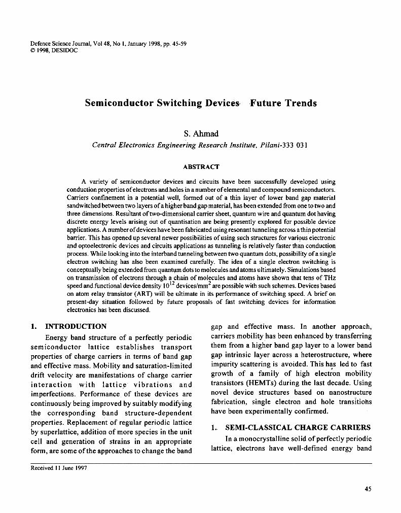
description I. In the form of a perfect-basedsemiconductor lattice, conduction and valence bandenergy vs wave vector relationships for all relevantsemiconducting materials, have been studied.Energy band diagrams of a few commonly usedsemiconductors are given in Fig. 1. Electrons andholes in semiconductors are attached to a finite
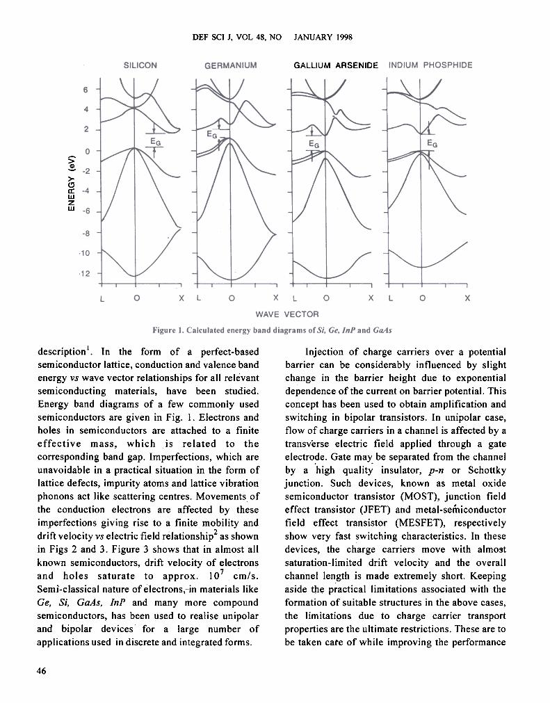
effective mass, which is related to thecorresponding band gap. Imperfections, which areunavoidable in a practical situation in the form oflattice defects, impurity atoms and lattice vibrationphonons act like scattering centres. Movements ofthe conduction electrons are affected by theseimperfections giving rise to a finite mobility anddrift velocity vs electric field relationship2 as shownin Figs 2 and 3. Figure 3 shows that in almost allknown semiconductors, drift velocity of electronsand holes saturate to approx. 107 cm/s.Semi-classical nature of electrons,-in materials likeGe, Si, GaAs, InP and many more compoundsemiconductors, has been used to realise unipolarand bipolar devices for a large number ofapplications used in discrete and integrated forms.
Injection of charge carriers over a potentialbarrier can be considerably influenced by slightchange in the barrier height due to exponentialdependence of the current on barrier potential. Thisconcept has been used to obtain amplification andswitching in bipolar transistors. In unipolar case,flow of charge carriers in a channel is affected by atransverse electric field applied through a gateelectro~e. Gate may. be separated from the channelby a high quality insulator, p-n or Schottkyjunction. Such devices, known as metal oxidesemiconductor transistor (MOST), junction fieldeffect transistor (JFET) and metal-seiniconductorfield effect transistor (MESFET), respectivelyshow very fast switching characteristics. In thesedevices, the charge carriers move with almostsaturation-limited drift velocity and the overallchannel length is made extremely short. Keeping
aside t!te practical limitations associated with theformation of suitable structures in the above cases,the limitations due to charge carrier transportproperties are the ultimate restrictions. These are tobe taken care of while improving the performance
46
AHMAD: SEMICONDUCTOR SWITCHING DEVICES-FUTURE TRENDS
TEMPERATURE
300 K'in"Eu
1'-0---
~UO-JW>
.-~a:C
100.000 .lnSb
Ga 0.47 In 0.53 As
InP
.ELECTRON
.HOLE
'/.lnA8
0 10.000>
N-E9
~ 1000~mO~
.GoAl
.lnP
aaSb.
.a.
.
v.InSb
G.Sb
.
0.1
.
CdTo
Si AISb
...ZnTo CdS..
GoAl AIAI. .ZnS.
...AISb GoP
InP I
.ZnTo
CdTo
.InA.
, In 0.53 As
Ga 0.47 TEMPERATURE
ELECTRON ~ 300 K
InP HOLE
J , ~ ~
1.0 10.0 100.0
ELECTRIC FIELD (KV/cm)
.ZnS
100 Figure 3. Drift velocities of electrons and holes as a function ofelectric field in a number of commonly usedsemiconductors at 300 K.
various fields of electronics. Materials growth has
matured to the extent that nonatomic layer epitaxial
growth are realised in molecular beam epitaxy
(MBE)5 and atomic layer epitaxy (ALE)6techniques on one hand and 500 mm diameter Si
wafers are produced commercially for various
applications on the other. Almost zero-defect
density bulk crystals are available for device and
circuit fabrications.
I. ZnS.
.CdS ZnS1 O ., ..r ' , , .I. ., .I' ., .I' ., , I' , , , I' , ., I' ~ , .
O 1 2 3 4
MINIMUM BANDGAP (eV)
Figure 2. Room temperature electron and hole mobilities in a
number of commonly used semiconductors.
of such devices. For example, saturation-limitedvelocity , which is almost fixed at 107 cm/s, is onesuch restriction. Similarly, mobilities of theelectrons and holes in most of the semiconductorsare only related to effective masses, which aregenerally not much different from free-electronmass except in few cases. Therefore, some othermechanism of improving upon the transportproperties of the charge carriers should be exploitedfor extending the performances of such families ofdevices and circuits to a state better than 'the present
one.
2. BAND STRUCTURE MODIFICA TIONS
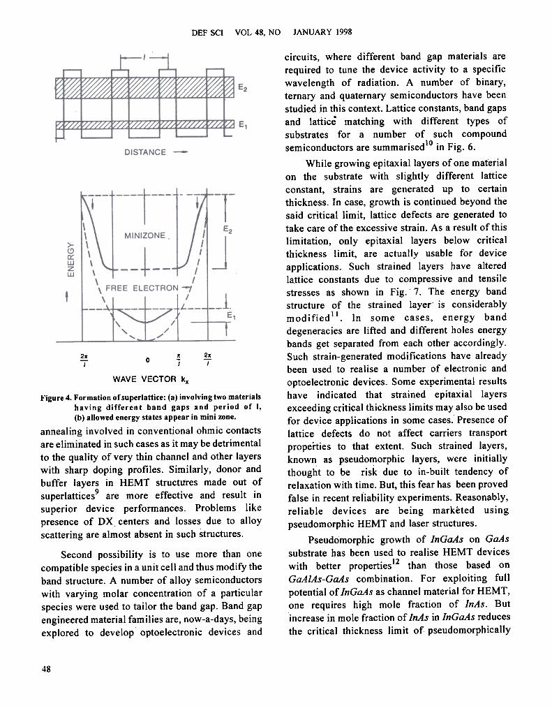
First step towards modification of energy-banddiagram of a semiconductor was to change thelattice periodicity by superimposing anotherperiodicity over the basic one. For example, onecould take alternate layers of two types ofsemiconductor lattices A and B, at regular interval,to approximate a situation similar to ABsemiconductor lattice. Such possibilities could bemany and accordingly, their band structu'te could be
estimated using well-known Kronig-Penny model7.These synthetic lattices do possess additionalfeatures and are known as superlattices. Effects 7
may be realised by choosing appropriate constituentsemiconductors in binary, ternary, quaternary andmore complex forms as shown in Figs 4 and 5. Insuperlattices, effective mass and band gap can bemodified to suit different requirements. Forexample, superlattices based non-alloyed ohmiccontacts8 are being investigated for quantum effect
compound semiconductor devices. High temperature
By improving the overall material quality andstructure formations in device processing,impressive performances have been achieved in
cases of bipolar and unipolar devices. Switchingspeeds in the range of picoseconds, gate length ofthe order of 50 nm in MOST and extremely denseVLSI circuits are the results of such improvements3.In case ofhigh electron mobility transistor (HEMT)devices, 1.2 dB noise figure at 94 GHz and cut-offfrequency above 200 GHz have been evidenced4.Discrete devices and integrated circuits have beenused in rea1ising very high performance systems in
47
0
0.
0
.1
01
JANUARY 1998DEF SCI VOL 48, NO
2JtI
21tI
!!0
WAVE VECTOR kx
Figure 4. Formation ofsuperlattice: (a) involving two materialshaving different band gaps and period of I,(b) allowed energy states appear in mini zone.
annealing involved in conventional ohmic contacts
are eliminated in such cases as it may be detrimental
to the quality of very thin channel and other layers
with sharp doping profiles. Similarly, donor and
buffer layers in HEMT structures made out of
superlattices9 are more effective and result in
superior device performances. Problems like
presence of OX centers and losses due to alloy
scattering are almost absent in such structures.
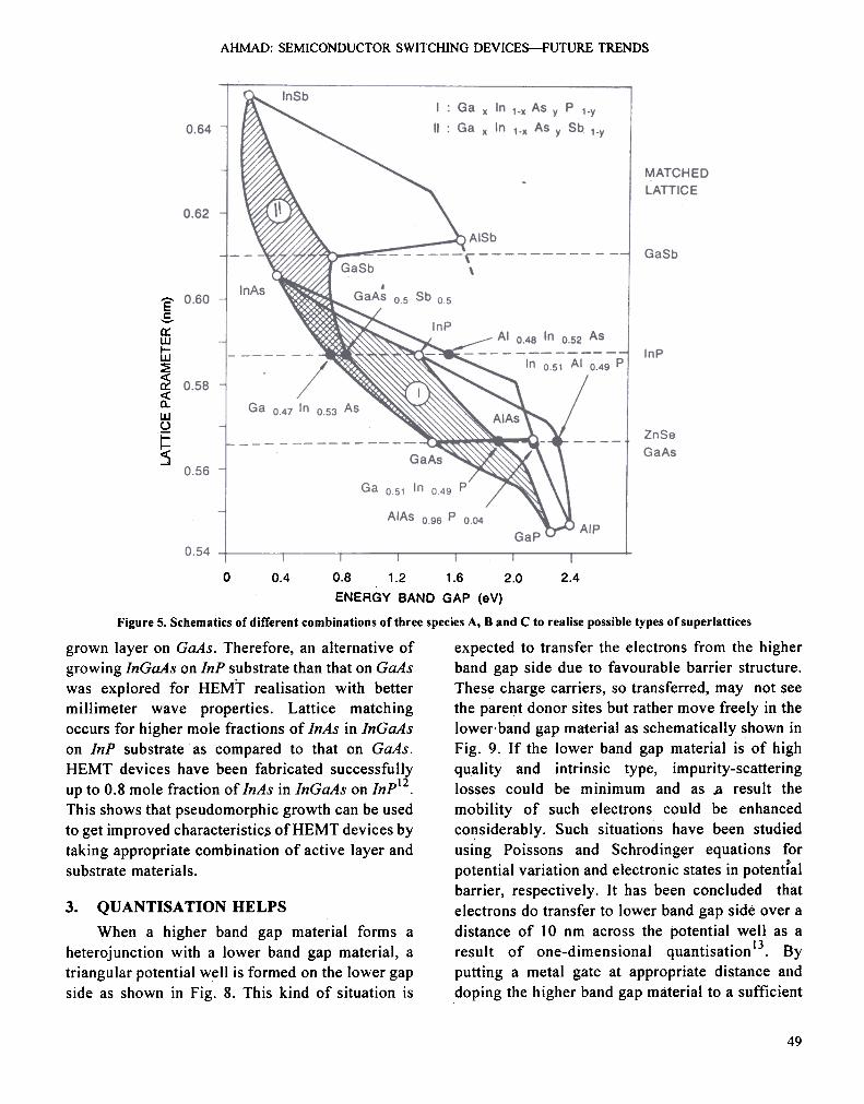
circuits, where different band gap materials arerequired to tune the device activity to a specificwavelength of radiation. A number of binary,ternary and quaternary semiconductors have beenstudied in this context. Lattice constants, band gapsand lattice" matching with different types ofsubstrates for a number of such compoundsemiconductors are summarised1O in Fig. 6.
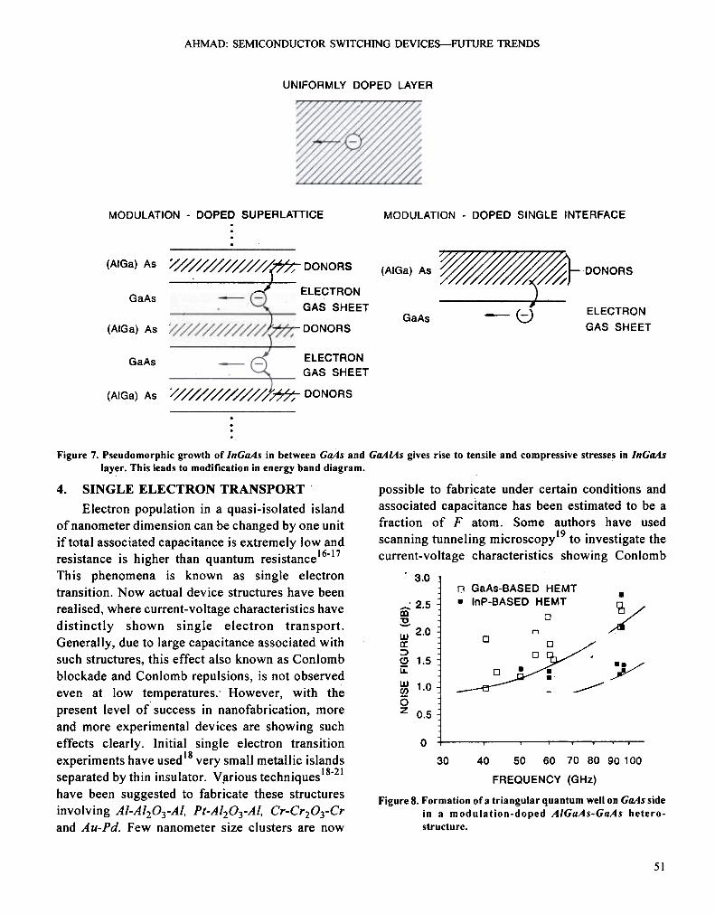
While growing epitaxial layers of one materialon the substrate with slightly different latticeconstant, strains are generated up to certainthickness. In case, growth is continued beyond thesaid critical limit, lattice defects are generated totake care of the excessive strain. As a result of thislimitation, only epitaxial layers below criticalthickness limit, are actually usable for deviceapplications. Such strained layers have alteredlattice constants due to compressive and tensilestresses as shown in Fig. 7. The energy bandstructure of the strained layer' is considerablymodified11. In some cases, energy banddegeneracies are lifted and different holes energybands get separated from each other accordingly.Such strain-generated modifications have alreadybeen used to realise a number of electronic andoptoelectronic devices. Some experimental resultshave indicated that strained epitaxial layersexceeding c{itical thickness limits may also be usedfor device applications in some cases. Presence oflattice defects do not affect carriers transportproperties to that extent. Such strained layers,known as pseudomorphic layers, were initiallythought to be risk due to in-built tendency ofrelaxation with time. But, this fear has been proved
false in recent reliability experiments. Reasonably,reliable devices are being marketed usingpseudomorphic HEMT and laser structures.
Pseudoinorphic growth of InGaAs on GaAssubstrate has been used to realise HEMT deviceswith better propertiesl2 than those based onGaA1As-GaAs combination. For exploiting fullpotential of InGaAs as channel material for HEMT ,one requires high mole fraction of InAs. Butincrease in mole fraction of InAs in InGaAs reduces
the critical thickness limit of pseudomorphically
Second possibility is to use more than onecompatible species in a unit cell and thus modify the
band structure. A number of alloy semiconductorswith varying molar concentration of a particularspecies were used to tailor the band gap. Band gap
engineered material families are, now-a-days, beingexplored to develop optoelectronic devices and
48
AHMAD: SEMICONDUCTOR SWITCHING DEVICES-FUTURE TRENDS
EcQ:w1-W~
~c{0..w~
§
0 0.4 0.8 1.2 1.6 2.0 2.4
ENERGY BAND GAP (eV)
Figure 5. Schematics of different combinations of three species A, B and C to realise possible types of superlattices
grown layer on GaAs. Therefore, an alternative of expected to transfer the electrons from the higher
growing InGaAs on InP substrate than that on GaAs band gap side due to favourable barrier structure.
was explored for HEMT realisation with better These charge carriers, so transferred, may not see
millimeter wave properties. Lattice matching the parent donor sites but rather move freely in the
occurs for higher mole fractions oflnAs in InGaAs lower.band gap material as schematically shown in
on InP substrate as compared to that on GaAs. Fig. 9. If the lower band gap material is of high
HEMT devices have been fabricated successfully quality and intrinsic type, impurity-scattering
up to 0.8 mole fraction of InAs in InGaAs oh Inpl2. losses could be minimum and as .a result the
This shows that pseudomorphic growth can be used mobility of such electrons could be enhanced
to get improved characteristic$ ofHEMT devices by considerably. Such situations have been studied
taking appropriate combination of active layer and using Poissons and Schrodinger equations for
substrate materials. potential variation and electronic states in potentral
barrier, respectively. It has been concluded that3. QUANTISATION HELPS electrons do transfer to lower band gap side over a
When a higher band gap material forms a distance of 10 nm across the potential well as a
heterojunction with a lower band gap material, a result of one-dimensional quantisation 13. By
triangular potential well is formed on the lower gap putting a metal gate at appropriate distance and
side as shown in Fig. 8. This kind of situation is doping the higher band gap material to a sufficient
49
DEF SCI J, VOl 48, NO JANUARY 1998
III III I I II II In~aAS
TENSILEO
Figure 6. Lattice constants,energy gaps and possible alloy semi-conductors having lattice matching to GaAs, InP,GaSh and ZnSe.
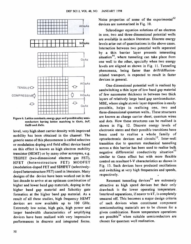
level, very high sheet carrier density with improvedmobility has been obtained in the channel. Thegeneric name of this phenomenon is called selectiveor modulation doping and field effect device basedon this effect is known as high electron mobilitytransistor (HEMT) or by many other acronyms, e.g.TEGFET (two-dimensional electron gas FET),HFET (heterostructure FET) MODFET(modulation-doped FET and SDHFET (selectively-doped heterostructure FET) used in literature. M~nydesigns of the device have been worked out in thelast decade to arrive at an optimum combination ofhigher and lower band gap materials, doping in the
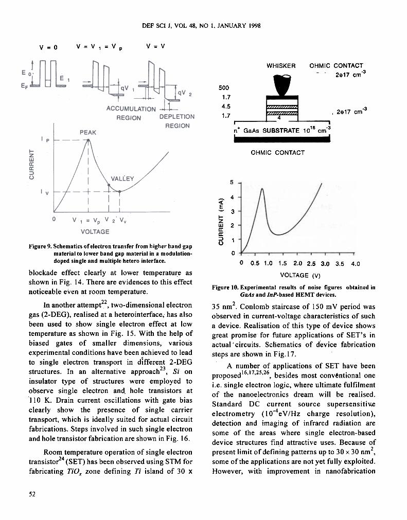
higher band gap material and Schottky gateformation at the higher band gap material. As aresult of all these studies, high frequency HEMTdevices are now available up to 100 GHz.Extremely low noise, high gain, high power andlarger bandwidth characteristics of amplifyingdevices have been realised with very impressiveperformances in discrete and integrated forms.
Noise properties of some of the experimental12devices are summarised in Fig. 10.
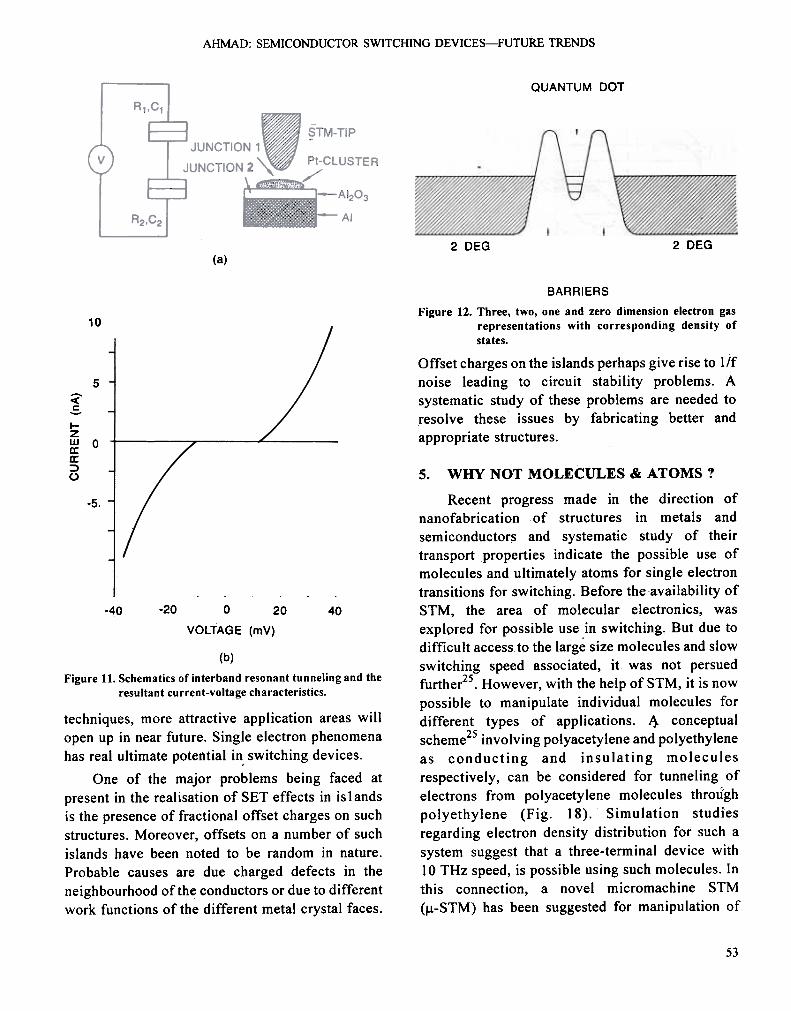
Schrodinger equation solutions of an electronin one, two and three-dimensional potential wellsare available in modern literature. Discrete energylevels arise out of quantisations in the above cases.Interaction between two potential wells separatedby a thin barrier layer presents interestingsituation 14, where tunneling can take place fromone well to the other, specially when two energylevels are aligned as shown in Fig. II. Tunnelingphenomena, being faster than drift/diffusion-related transport, is expected to result in fasterdevices in general.
One-dimensional potential well is realised bysandwitching a thin layer of low band gap materialof few nanometer thickness in between two thicklayers of relatively large band gap semiconductor.MBE, where single atomic layer deposition is easilypossible, helps in realising o~e, two andthree-dimensipnal quantum wells.. These structuresare known as charge carrier sheet, quantum wiresand dots. How these structures can be realised isshown in Fig. 12. Discrete energy levels ofelectronic states and their possible transitions havebeen used to realise a whole family ofoptoelectronic devices and circuitsl2. Inter-welltransition due to quantum mechanical tunnelingacross a thin barrier has been used to realise bulknegative differential conductivity situation 15
similar to Gunn effect but with more flexiblecontrol on resultant- I- V characteristics as shown inFig. 13. Such devices have produced oscillationsand switching at very high frequencies and speeds,
respectively.R I . d .14
Iesonant tunne Ing evlCes are extreme yattractive as high speed devices but their only
drawback is the lower operating temperature.Interlevel separations, if nearer to kT, is completelysmeared off. This becomes a major design criteriaof such devices when constituent componentsemiconducting materials are to be chosen for a
given combination. Room temperature operationsare possible14 when suitable semiconductors arechosen for quantum well realisation.
50
AHMAD: SEMICONDUCTOR SWITCHING DEVICES--FUTURE TRENDS
UNIFORMLY DOPED LAYER
MODULATION -DOPED SUPERLATTICE MODULATION -DOPED SINGLE INTERFACE
'// / / / / / / // / / / /~ DONORS
.-;:!ELECTRONGAS SHEET
W DONORS
(AlGa) As(AlGa) As ~ ,.- DONORS
GaAs
-8 ELECTRONGAS SHEET
GaAs(AlGa) As '////////////~
(AlGa) As '//////////////~ DONORS
GaAs
Figure 7. Pseudomorphic growth of InGaAs in between GaAs and GaAL4s gives rise to tensile and compressive stresses in InGaAslayer. This leads to modification in energy band diagram.
SINGLE ELECTRON TRANSPORT possible to fabricate under certain conditions and
Electron population in a quasi-isolated island associated capacitance has been estimated to be a
of nanometer dimension can be changed by one unit fraction of F atom. Some authors have used
if total associated capacita~ce is extremely low and scanning tunneling microscopy19 to investigate the
resistance is higher than quantum resistancel6-17 current-voltage characteristics showing Conlomb
This phenomena is known as single electron. 3.0 ,
transition. Now actual device structures have beenrealised, where current-voltage characteristics have ~ 2.5
distinctly shown single electron transport. ~ 2.0
Generally, due to large capacitance associated with ~
such structures, this effect also known as Conlomb a 1.5blockade and Conlomb repulsions, is not observed ~
even at low temperatures.' However, with the ~ 1.0
present level of'success in nanofabrication, more ~ 0.5
and more experimental devices are showing such
effects clearly. In itial single electron transition 0
experiments have used18 very small metallic islandsdb h .. I V . h .18-21 separate y t In Insu ator. .aflOUS tec nlques
have been suggested to fabricate these structures
involving Al-AI203-Al, Pt-AI203-Al. Cr-Cr203-Crand Au-Pd. Few nanometer size clusters are now
4.
D GaAs-BASED HEMT
.InP-BASED HEMT
D
.
y0o o
~
/
y
~
-
30 40 50 60 70 80 90100
FREOUENCY (GHz)
Figure 8. Formation of a triangular quantum well on GaAs sidein a modulation-doped AIGaAs-GaAs hetero-structure.
51
ELECTRON
GAS SHEET
DEF SCI J, VOl 48, NO I, JANUARY 1998
V=V1=Vpv = vv = 0
WHISKER
500
1.7
4.5
1.7
-3n-GaAs, 2917 cm
..c:.Y::-
n+ GaAs SUBSTRATE 1018.3
cm
OHMIC CONTACT
5
<.§.f-zw[I;[I;::>u
4
3
2
O
0 0.5 1.0 1.5 2.0 2.5 3.0 3.5 4.0
VOLTAGE (V)
Figure 10. Experimental results of noise figures obtained inGaAs and InP-based HEMT devices.
35 nm2. Conlomb staircase of 150 m V period was
observed in current-voltage characteristics of such
a devjce. Realisation of this type of device shows
great promise for future applications of SET's in
actual. circuits. Schematics of device fabrication
steps are shown in Fig.17 .
A number of applications of SET have been
proposedI6,17,25,26, besides most conv~ntional one
i.e. single electron logic, where ultimate fulfilment
of the nanoelectronics dream will be realised.
Standard DC current source supersensitiv-e
electrometry ( I 0-4e V IHz charge resolution),
detection and imaging of infrared radiation are
some of the areas where single electron-based
device structures find attractive uses. Because of
present limit of defin"ing patterns up to 30 x 30 nm2,
some of the applications are not yet fully exploited.
However, with improvement in nanofabrication
Figure 9. Schematics of electron transfer from higher band gapmaterial to lower band gap material in a modulation-doped single and multiple hetero interface.
blockade effect clearly at lower temperatur:e as
shown in Fig. 14. There are evidences to this effect
noticeable even at room temperature.
In another attempt22, two-dimensional electron
gas (2-DEG), realised at a heterointerface,o has also
been used to show single electron effect at low
temperature as shown in Fig. 15. With the help of
biased gates of smaller dimensions, various
experimental conditions have been achieved to lead
to single electron transport in different 2-DEG
structures. In an alternative approach23, Si on
insulator type of structures were employed to
observe single electron and. hole transistors at
0110 K. Drain current oscillations with gate bias
clearly show the presence of single carrier
transport, which is ideally suited for actual circuit
fabrications. Steps involved in such single electron
and hole transistor fabrication are shown in Fig. 16.
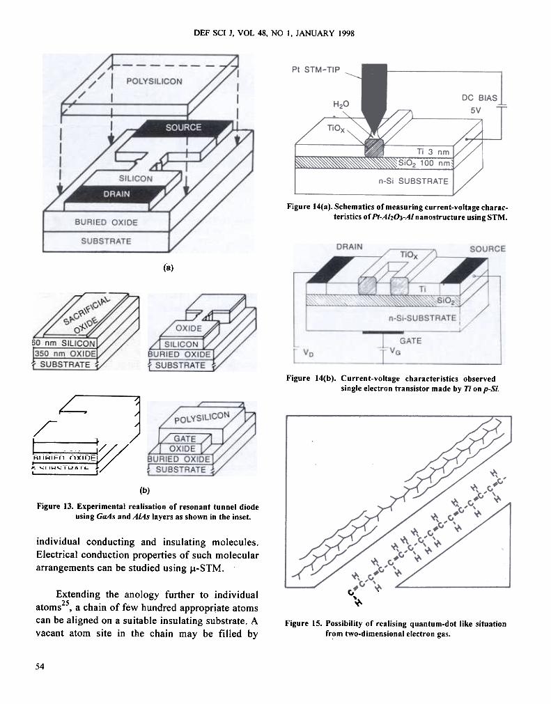
Room temperature operation of single electron
transistor24 (SET) has been observed using STM for
fabricating TiOx zone defining Ti island of 30 X
52
nm
nm
nm
nm
OHMIC CONTACT.3
n-GaAs, 2817 cm
AlAs
GaAs
AlAs
AHMAD: SEMICONDUCTOR SWITCHING DEVICES-FUTURE TRENDS
QUANTUM DOT
2 DEG2 DEG(a)
BARRIERS
Figure 12. Three, two, one and zero dimension electron gasrepresentations with corresponding density ofstates.
10
T = 1.8 K
Offset charges on the islands perhaps give rise to l/fnoise leading to circuit stability problems. Asystematic study of these problems are needed toresolve these issues by fabricating better andappropriate structures.
5
<-=-1-
ffi oa:a:;:)<.> 5. WHY NOT MOLECULES & ATOMS ?
Recent progress made in the direction ofnanofabrication of structures in metals andsemiconductors and systematic study of theirtransport properties indicate the possible use ofmolecules and ultimately atoms for single electrontransitions for switching. Before the availability ofSTM, the area of molecular electronics, wasexplored for possible use in switching. But due to.difficult access to the large size molecules and slowswitching speed associated, it was not persuedfurthe15. However, with the help ofSTM, it is nowpossible to manipulate individual molecules for
different types of applications. ~ conceptualscheme25 involving polyacetylene and polyethyleneas conducting and insulating moleculesrespectively, can be considered for tunneling ofelectrons from polyacetylene molecules throughpolyethylene (Fig. 18). Simulation studiesregarding electron density distribution for such asystem suggest that a three-terminal device with10 THz speed, is possible using such molecules. Inthis connection, a novel micromachine STM(J.1-STM) has been suggested for manipulation of
-5.
I I I I I I I I
-40 -20 0 20 40
VOLTAGE (mV)
(b)
Figure 11. Schematics of interband resonant tunneling and the
resultant current-voltage characteristics.
techniques, more attractive application areas willopen up in near future. Single electron phenomenahas real ultimate potential in, switching devices.
One of the major problems being faced atpresent in the realisation of SET effects in is 1 andsis the presence of fractional offset charges on suchstructures. Moreover, offsets on a number of suchislands have been noted to be random in nature.Probable causes are due charged defects in theneighbourhood of the conductors or due to differentwork functions of the different metal crystal faces.
53
DEF SCI J, VOl 48, NO 1, JANUARY 1998
L
~
POLYSlLICON('/
1//
1,'
I~
SILICON
Figure 14(a). Schematics of mea$uring current-voltage charac-teristics of Pt-AhO3-AI nanostructure using STM.
BURIED OXIDE
SUBSTRATE
(8)
13~~ 1~r:...~~~gE."4' SUBSTRATE :
Figure 14(b). Current-voltage characteristics observedsingle electron transistor made by Ti on p-Si.
~BURIED OXIDEW
~ SUBSTRATE {/
SILICON
~~ ..#c,'
\ ,"
~ c,#c, '+~ #c,' ,\ ,C' "'
~ c, \'\\ '"' , c, # "'
~ c,'C" ~~ c,#C" ~ +
c,' ,+\ c,# ~
c,' ,c,# "'
'+
(b)
Figure 13. Experimental realisation of resonant tunnel diode
using GaAs and A/As layers as shown in the inset.
individual conducting and insulating molecules.Electrical conduction properties of such moleculararrangements can be studied using I.1-STM.
Extending the anology further to individualatoms2S, a chain of few hundred appropriate atomscan be aligned on a suitable insulating substrate. Avacant atom site in the chain may be filled by
Figure 15. Possibility of realising quantum-dot like situationfr~m two-dimensional electron gas.
54
AHMAD: SEMICONDUCTOR SWITCHING DEVICES-FUTURE TRENDS
OFF
~
ON
~
MOSES
SINGLE
I/ELECTRONi DEVICES
MOLECULAR (SET) ~
DEVICES
INTEGRATED
CIRCUITS
(MOS)
ATOM WIRE SWITCHING GATE
\ ;,p- ~
O::X~D CXXXX) cxxxx:o
&-. "SWITCHING ATOM.;s;;7~
8 ~ RESET GATE -vg
QUANTUM
DEVICES
~I SUPER-
D CONDUCTOR
DEVICESD TRANSISTORSRELAYS VACUUM TUBES
d
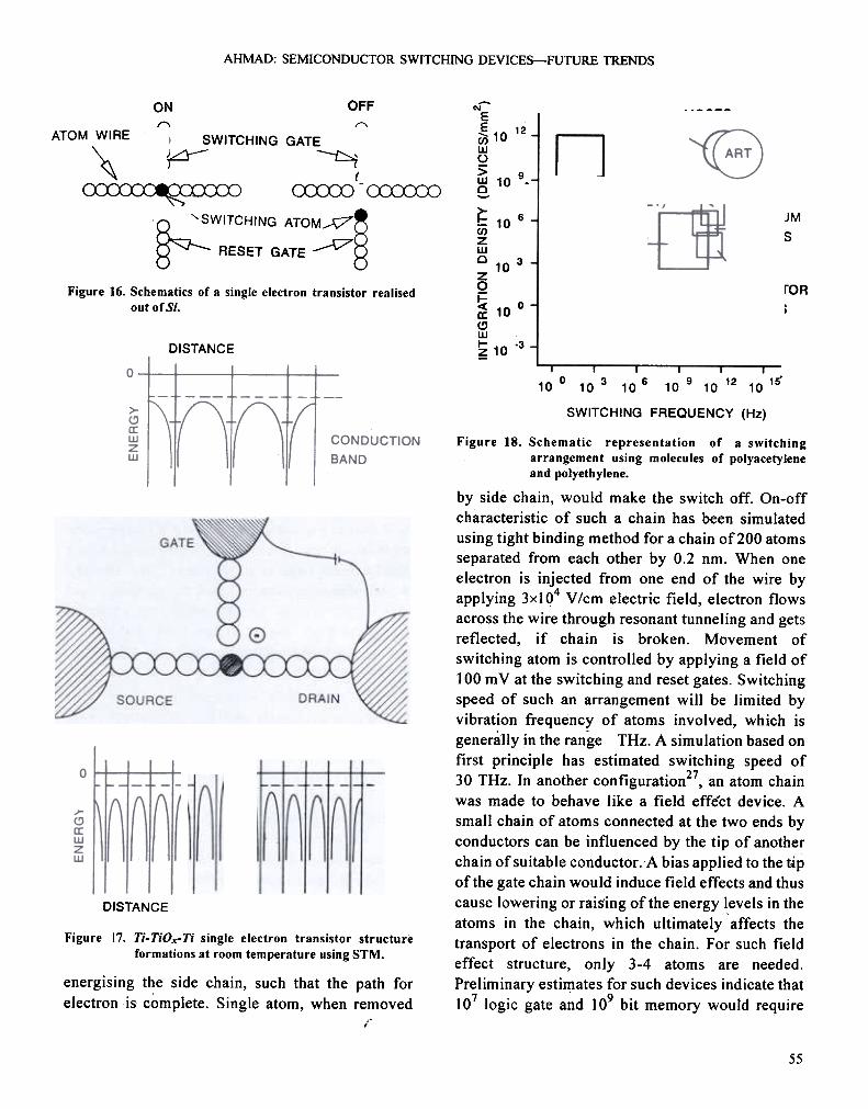
Figure 16. Schematics of a single electron transistor realised
out of Si.
~N
EE-
(/)wU
>w
e.
~(/)ZwQ
a
~a:(!)w1-~
DISTANCE
10 o103 106 109 1012 1015'
SWITCHING FREOUENCY (Hz)
Figure 18. Schematic representation of a switchingarrangement using molecules of polyacetyleneand polyethylene.
by side chain, would make the switch off. On-offcharacteristic of such a chain has been simulatedusing tight binding method for a chain of200 atomsseparated from each other by 0.2 nm. When oneelectron is injected from one end of the wire byapplying 3xl04 V /cm electric field, electron flowsacross the wire through resonant tunneling and getsreflected, if chain is broken. Movement ofswitching atom is controlled by applying a field of100 m Vat the switching and reset gates. Switchingspeed of such an arrangement will be limited byvibration frequency of atoms involved, which isgenerilly in the range THz. A simulation based onfirst principle has estimated switching speed of30 THz. In another configuration27, an atom chainwas made to behave like a field effect device. Asmall chain of atoms connected at the two ends byconductors can be influenced by the tip of anotherchain of suitable conductor. A bias applied to the upof the gate chain would induce field effects and thuscause lowering or rais'ing of the energy I,evels in theatoms in the chain, which ultimately affects thetransport of electrons in the chain. For such fieldeffect structure, only 3-4 atoms are needed.Preliminary estimates for such devices indicate that107 logic gate and 109 bit memory would require
DISTANCE
Figure 17. Ti-TiOrTi single electron transistor structureformations at room temperature using STM.
energising the side chain, such that the path for
electron is complete. Single atom, when removed
,
55
10
10
10
10
10
10
12
9
6
3
O
.3
DEF SCI I, VOL 48, NO JANUARY 1998
lithographies48. For example, electron-beamlithography can lead to 10 nm feature sizes withsuitable modifications. Focussed ion beam (FIB)lithography has also been proven to go to the samelimit of 10 nm. Excimer laser and synchrotronradiation (SR)-based experiments indicate limit tofew tens of nanometer. Scanning transmission andtunneling microscopic modes are expecte.d toenhance the limit to I and 0.1 nm, respectively. Anumber of resists have been tried out withencouraging results. Well-known PMMA resolves8 nm features, whereas ZEP and SAL-601 resistscould produce 20 nm features in positive andnegative modes. Inorganic resists like AIF3, NaCIand S;O2 have also been used with scanningtunneling electron microscopy (STEM)arrangement. Carbon patterns have been realised tothe size of 8 nm in scanning electron microscopy(SEM). A similar size pattern has been made using
+PMMA and Ga FIB lithography.
A 50 KY electron beam system29 using thermalfield emitter gun consisting of Zr/0/W is reported toproduce 10 nm lines with 50 nm period usingPMMA resist. Feeding styrene gas (C6H8CH=CH2)in. the above system, C patterns ranging from14-150 nm could be deposited by changingirradiation time. Such C films could be used asetching mask in transferring nano size pa,tterns to
semiconductors.
FIBs have been developed for lithographicpurposes with certain definite advantages overelectron beam. Exposure sensitivity of ion beam istwo orders of magnitude higher and there ispractically negligible ion scattering in the resist andvery low backscattering from the robstrate. Asystem28 using 50 KeY Ga+ beam having reducedchromatic aberration has been shown to produce7-8 nm features in 30 nm PMMA on GaAs withthroughput equal to state-of-the-art electron beam
setup.
20 !lm2 and 2002 !lm, respectively. Longest signaldelay will not exceed 10-12 s on such a chip of200 !lm2. Therefore, THz operation is easilypossible on such a chip.
A comparison of molecular and atomicswitching devices, termed as molecular singleelectron switching (MOSES) and atom relaytransistor (ART), along with other conventionaldevices, clearly indicate the superior position ofsuch devices for future information electronics
I ..25app lcatlons .
Realisation of MOSES and ART- devices doesnot seem to be an impossibility. Continuous effortsbeing made in the area of materials growth-Iikeatomic layer epitaxy and self-organised growtharising out of highly strained layers, nanolitho-graphy involving electron beam, ion-beam andX-ray and nonconventional methods and novelcontact fabrication techniques based on superlattice
/non-alloyed structure, do indicate that such devicescan be fabricat~d in near future. Recent success offabricating quantum wire and dots with regularbehaviour of electronic conduction observed inthese structures instills a hope for future succ.ess.
6. MATCHING FABRICATIONTECHNOLOGY
Quantum effect-based device behaviourpredictions can be verified only by fabricating suchstructures of nano and atomic sizes initially asisolated structures to resolve various issuesinvolved. Next comes the utilisation of thisknowledge to realise useful device structures fortheir exploitation in functional circuit modules. Forthese, a lithography technique, similar to the onealready in use in various forms, has to be developedto handle pattern delineation on the given materialwith a suitable combination of resist layer patternforming methodology and finally structureformation. Recent developments taking place in thisdirection are interesting as there seems to emergesome deviations from the conventional techniques.Figure 22 shows the requirements of submicron,nano and atom technologies along with theresolution of electron, ion and photon-based
Atomic layer etching involving reactive gas
physiosorption, low energybeam-induced reaction
and desorption of reaction products, has recently
been investigated for defining nano size patterns for
device applications28. GaAs has been etched while
56
AHMAD: SEMICONDUCTOR SWITCHING DEVICES-FUTURE TRENDS
feeding Cl2 gas continuously and applying layerpulses in atomic layer etching mode. Similarly,employing low energy Ar+ pulses in place of laser,digital etching has been observed28 in GaAs. Siatomic layer etching has been observed28 when Fatoms are adsorbed on Si surface at low temperatureand subsequently 20 e V Ar + irradiation is produced.
Ar+ are produced by remote cyclotron resonanceplasma (ECR) and F atoms are released bymicrowave plasma involving CF 4 + 4% 02.
STM has been used in various modes tomanipulate atoms for patterning purposes. In a STMsystem, cooled to 4 K, tip is lowered to increaseatom-tip interaction and tben tip is moved at0.4 nm/s to the desired location and finally the tip iswithdrawn by going into imaging Diode. Xe atomsand CO molecules have been moved to desiredlocation using this techniqye28. Similarly, byapplying large electric field to the tip of a field ionmicroscope, it was possible to evaporate protrudingsurface atoms as ions. S from MoS2 and Se fromWSe are reported to be evaporated in thismanner28.Si atoms could be extracted from Si ( III )7x7surface and relocated3o. Au STM tip has been usedas a nanometer size Au structures31. Here also, theemission process is believed to be of fieldevaporation type. W patterns have been depositedby STM using W(CO)6 organometallic gas.Similarly, WF6 gas ambient provided Si substrateetching using STM28.
20 nm periodicity could be fabricated by ion millingof coated protein surface.
In self-assembled lithograply28, a monolayerfilm of organosilane is coated on the semiconductorsurface b)"any one of the methods like dip, spinningor vapour deposition technique, as shown in Fig. 21.This monolayer film is patterned by anyone of thesources like deep UY, ArF ( 193 nm), KrF (248 nm)lasers, X-ray, electron, ion beams and STM. Thelatent image in the organosilane film is metallisedin electroless deposition using Pd/Sn as catalystfollowed by metal deposition. Plasma etchingproduces patterns in the substrate subsequently.
Atomic layer lithography uses a nonatomiclayer as resisr8. In an experiment, a freshlyprepared surface of GaAs was oxidised usinghalogen lamp and O2 ambient over a period of 1 hr .This thin layer of GaAs oxide was patterned byelectron-beam in the presence of Cl2 underpressure. Thus, very fine patterns were delineartedusing GaAs oxide mask. In another set ofexperimenr8, a clean Si wafer was dipped inHF:H2O: : 1: lOO, followed by rinse in ultrapure Dlwater. This atomic H termination on Si surface wasused as resist layer for lithography. In the followingstep, electron beam exposure removed H-tennina-tion and fonned the required pattern. Al isselectively deposited on rest of H-terminated areaof the substrate after oxidising the H desorbedsurf~ce due to electron-beam exposure by takingout the wafer to nornal.ambient temperature in
clean'room.
Wavelength of an energetic electron isgenerally very small. For example, 200 KeYelectron possesses 0.087 nm wavelen-gth. For suchsituations, a hologram can be produced with
subangstrom fring~ spacings28. Using magnifiedfringe spacings, nanoscale pattern can be generatedby electron holography. Some preliminary records
of such holograms are encouraging.
28dSome novel techniques have been reporte
recently in connection with nanolithography.Natural lithography, self-assembled lithography,atomic layer lithography and electron holographyare some interesting techniques catching attention.
In natural lithography28, a nondispessivecolloid of controllable size is coated on the surfaceof the semiconductor instead of a resist. An orderedarray of 0.8 J.lm spheres has been produced by spincoating of 15 per cent latex polystyrene(C6HsCHCH2)x on Si substrate at 2400 rpm. Even,protein crystals have been coated and driedfollowed by shadow deposition of Ti at 50° from thenormal and a hexagonal array of 10 nm holes with a
7. CONCLUSIONS
Systematic uQderstanding of electron transportin ideal bulk semiconductor followed bymodifications in energy-band structure due to
57
DEF SCI J, VOL 48, NO I, JANUARY 1998
superlattice, change in composition in unit cell andstrained lattices and ultimately trying one, two andthree-dimensional quantisations, indicated towardsadditional charge carrier features. Early successesin realising quantum charge career sheet, wire anddots, clearly indicate towards the possible extensionto molecular and atomic structures for switchingapplications, involving single electron or holetransitions. The way progress is being made indifferent areas, it seems quite probable to realisemolecular and atomic structures described in thispaper. Switching circuits, so realised, will haveenormous applications in diverse tieldswhich couldnot be feasible from today's standard. Systemdesign concepts would also need drastic change inmethodology in future.
8
edited by L.L. Chang and B.C. Giessen.Academic Press, Orlands, 1985. pp. 3-42,
Shen, T.C.; Gao, G.B. & Morkoc, H. Recentdevelopments in ohmic contacts for III- Vcompound semiconductors. .I: Vac. Sci. Technol.
1992,810(5),2113-32.
9
10.
Baba, T .; Mizutani, T. & Ogawa, M.AIAs/n-GaAs superlattice and its application tohigh quality two-dimensional electron gassystems. .I: App. Phys., 1986, 59(2), 526-32.
Swaminathan, V: & Macrander, A.T. Materialsaspects of GaAs and InP-based structures,Prentice Hall Advanced References Series:Engineering. Prentice Hall, Englewood Cliff,New Jersey, 1991. pp. 1-42,
Pollak, F .H. Effects of homogeneous strain on theelectronic and vibrational levels. InSemiconductors and semimetals, edited by T.P.Pearsall. Academic Press, Inc. Boston, 1990. pp.17-53
REFERENCES
12 Chao, P.C.; Swanson, A.; Brown, A.; Mishra, U.;Ali, F. & Yuen, C. HEMT devices and circuitapplications. In HEMTs and HBT6: devices,fabrication, and circuits, edited by F. Ali and A.Gupta. Artech House, Boston, 1991. pp.77-190.
2
133
Singh, J. Properties of semiconductors: Electronicstates, Zn, semiconductor optoelectronics:physic$ and technology. McGraw Hill, Inc., NewYork, 1995. pp.53-111.
Bean, J.C. Materials and technologies. In Highspeed semiconductor devices, edited by S.M. Sze.Wiley Interscience, John, Wiley and Sons' Inc.,New York, 1990. pp. 13-55
Ono, M.; Saito, M. & Yoshitomi, T. Fabricationof sub-50 nm gate length n-metal-oxide-semiconductor field effect transistors and theirelectrical characteristics.J Vac. Sc. Techn. 1995,B 13(4), 1740-43 14
Pearton, S.J. & Shah, N.J. Heterostructure fieldeffect transistors. In High speed semiconductordevices, edited by S.M. Sze. John Wiley andSons Inc., New York, 1990. pp. 283-333.
Capasso. F .; Sen, S. & Beltram, F. Quantumeffect devices. -In High speed semiconductordevices, edited by S.M. Sze. John Wiley and SonsInc., New York, 1990. pp. 465-520.
4. Takamiya, S.; Yoshida, N .; Hayafuji, N .; Sonoda,
T. & Mitsui,M. Overview of recent development
of HEMTs in the MM-wave range. Solid State
Electronics, 1995, 38(9), 1581-88. 15, Sze, S.M. Microwave diodes. In' High speedsemiconductor devices, edited by S.M. Sze. JohnWiley and Sons Inc., New York, 1990. pp.521-85.
5 Sakaki, H. Molecular beam epitaxy. In, III-V
Semiconductor materials and devices, edited by,R J. Malik. Elsevier Science Publisher B. V .,
1989. pp. 217-330. 16.
6. Suntola, T. Atomic layer epitaxy. Thin Solid
Films, 1992,216, 84-89.7.
Hadley, P.; Harrnans, C.J.P.M. & Mooij, J.E.
Single electronics: one electron, one bit. FEDJournal, 1994, 4 (Suppl.2), 20-27.
Likharev, K.K. Physics and possible applications
of single-electron devices. FED Journal, 1995,
6 (Suppl.1), 5-14.
7. Esaki, L. History perspectives of semiconductorsuperlattices. In Synthetic modulated structures,
58
AHMAD: SEMICONDUCTOR SWITCHING DEVICES-FUTURE TRENDS
18. Ji, L.; Dresselhaus, p .D.; Han, S.; Lin, K.; Zheng,W. & Lukens, J.E. Fabrication andcharacterisation of single electron transistors andtraps. J: Vac. Sci. Technol. 1994, B 12(6),3619-22.
.25. Wada, Y. Atom electronics: A proposal fornanoscale devices based on at om/moleculeswitching. Microelectronis Engineering, 1996,
30,375-82.
19.
20.
21
Kreupl, F.; Vancea, J.; Risch, L.; Hofmann, F. &Hoffmann, H. UltrasmalI Pt clusters for singleelectron tunneling studies. MicroelectronicEngineering, 1996, 30, 451-54.
Altmeyer, S.; Spangenberg, B.; Kuhnel, F. &Kurz, H. Step edge cut-off-Au: new fabricationprocess for metal-based single electron devices.Microelectronic Engineering, 1996, 399-402.
Chen, w. & Ahmad, H. F.abrication and physicsof -2 nm islands for single electron devices. .I:Vac. Sci. Technol., 1995, B 13(6), 2883-887.
26. Okaya{na, S.; Kimura, S.; Asai, A. & Maeda, S.Prospects, and status of MITI's quantumfunctional device project. MicroelectronicsEngineering, 1996,30, 17-26.
27. Kelly, M. Today's new materials: atomic controlin one dimension, prospects in nanotechnology,edited by M. Knnenacker and J. Lewis. JohnWiley and Sons, Inc., New York, 1995.pp. 129-46.
28. Matsui, S. Trends in nanostructure fabricationtechnology .FED Journal, 1994, 4 (Suppl.2),34-43.
22. 29. Ochiai, Y.; Baba, M.; Watanabe, H. & Matsui, S.Ten nanometer resolution nanolithography usingnewly developed SO-KeV electron beam directwriting system. Jpn. .I: App. Phys., 1991, 30,3266.
23
Huang, D.; Uchida, H. & Aono, M. Fabrication of
atomic scale structures on Si (111)- 7 x 7 using a
scanning tunneling microscope (STM). Jpn. J.ApplPhys., 1992,31 (12B), 4501-03.
30,
24.
Haug, R.J. & Klitzing, K. V. Prospects forresearch on quantam dots. and single elctrontransistors. FED Journal, 1995,6 (Suppl.2), 4-12.
Leobondung, E.; Guo, L.; Wang, Y. & Chou, S.Y.Single electron and hole quantum dot transistorsoperating above 110 K. J. Vac. Sci. Technol.,1995, B 13(6), pp 2865-868.
Matsumoto, K.; Ishii, M.; Segawa, K.; Ok&, y .;Vartanian B.J. & Harris, J.S. Room temperatureoperation of a single electron transistor made bythe scanning tunneJing microscope nanooxidation process for the TiOxlTi system. App.
Phys. Lett., 1996,8(1), 34-36,
31 Lebreton, C. & Wang, 2.2. Nanofabrication ongold surface with scanning tunneling microscopy.Microelectronic Engineering, 1996, 30, 391-94.
59