Semiconductor Reliability Topics for Leading Edge CMOS ... 2010.pdf · Semiconductor Reliability...
59
1 ' 2002 IBM Corporation IBM Systems and Technology Group - SRDC Semiconductor Reliability Topics for Leading Edge CMOS Technologies Fernando Guarín Ph.D. Semiconductor Research & Development Center IBM Systems and Technology Group 2070 Route 52, Hopewell Junction, NY 12533 [email protected]
Transcript of Semiconductor Reliability Topics for Leading Edge CMOS ... 2010.pdf · Semiconductor Reliability...
1
© 2002 IBM Corporation
IBM Systems and Technology Group - SRDC
Semiconductor Reliability Topics for Leading Edge CMOS Technologies
Fernando Guarín Ph.D. Semiconductor Research & Development CenterIBM Systems and Technology Group 2070 Route 52, Hopewell Junction, NY 12533
IBM Systems and Technology Group - SRDC
© 2010 IBM Corporation2 Tokyo 2010 (Guarín)
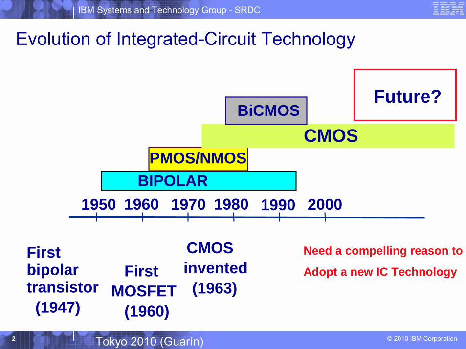
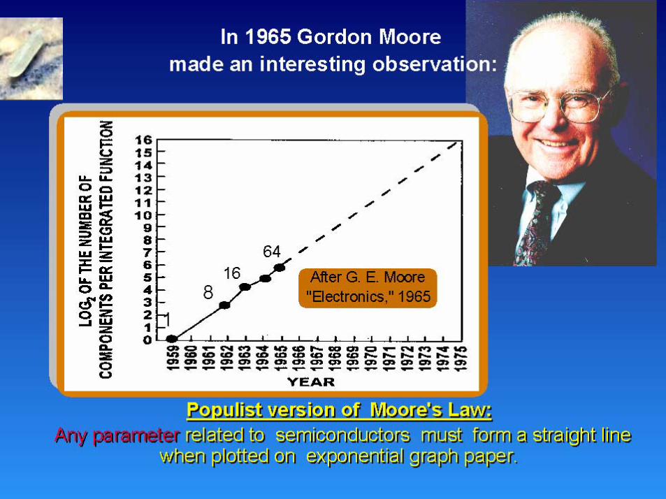
1950 19701960 19901980 2000
First bipolar transistor(1947)
First MOSFET
(1960)
CMOSinvented(1963)
BIPOLARPMOS/NMOS
CMOSBiCMOS
Evolution of Integrated-Circuit Technology
Future?
Need a compelling reason to
Adopt a new IC Technology
IBM Systems and Technology Group - SRDC
© 2010 IBM Corporation3 Tokyo 2010 (Guarín)
IBM Systems and Technology Group - SRDC
© 2010 IBM Corporation4 Tokyo 2010 (Guarín)
IBM Systems and Technology Group - SRDC
© 2010 IBM Corporation5 Tokyo 2010 (Guarín)
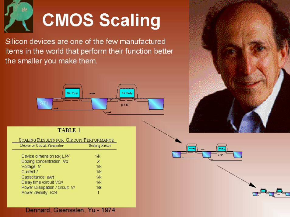
High-Field Effects Limit CMOS Scaling
! Ideally, scaling is to be done at constant field
! In practice, scaling has been achieved by increasing electric fields
! High gate oxide field " large gate tunneling current� Solution: High-k gate insulator
� New reliability challenges PBTI
IBM Systems and Technology Group - SRDC
© 2010 IBM Corporation6 Tokyo 2010 (Guarín)
Miniaturización � Scaling��Moore�s �Law� predicted ONLY continuous size decrease�Dennard�s Scaling theory predicted the performance increases associated with smaller device size�Moore provide the path and Dennard provided the way to implement it�The end is near has been a recurring theme in the semiconductor industry for many years.�First paper predicting the end was published by RCA over 30 years ago� We are still predicting the end
� Tunneling Current Increase at larger fields�High K to the rescue
� what is next?�3D, Fin Fets, ��. End of Silicon Scaling
�Atoms don�t scale !!
IBM Systems and Technology Group - SRDC
© 2010 IBM Corporation7 Tokyo 2010 (Guarín)
BipolarBipolar
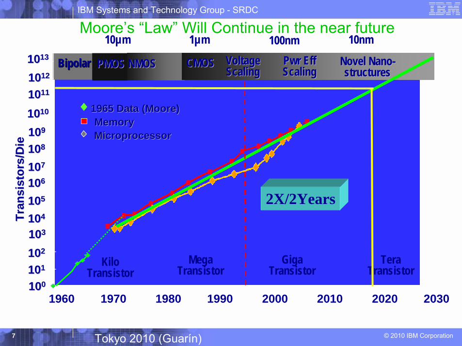
Moore�s �Law� Will Continue in the near future
1960 1970 1980 1990 2000 2010 2020 2030
CMOSCMOS
1µm 100nm 10nm10µm
PMOS PMOS
101088
101077
101066
101055
101044
101033
101022
101011
101000
101099
10101010 1965 Data (Moore)1965 Data (Moore)
MicroprocessorMicroprocessorMemoryMemory
1010111110101212
10101313 VoltageVoltageScalingScaling
PwrPwr EffEffScalingScalingNMOSNMOS
KiloTransistor
MegaTransistor
GigaTransistor
TeraTransistor
Tran
sist
ors/
Die
Tran
sist
ors/
Die
2X/2Years
Novel NanoNovel Nano--structuresstructures
IBM Systems and Technology Group - SRDC
© 2010 IBM Corporation8 Tokyo 2010 (Guarín)
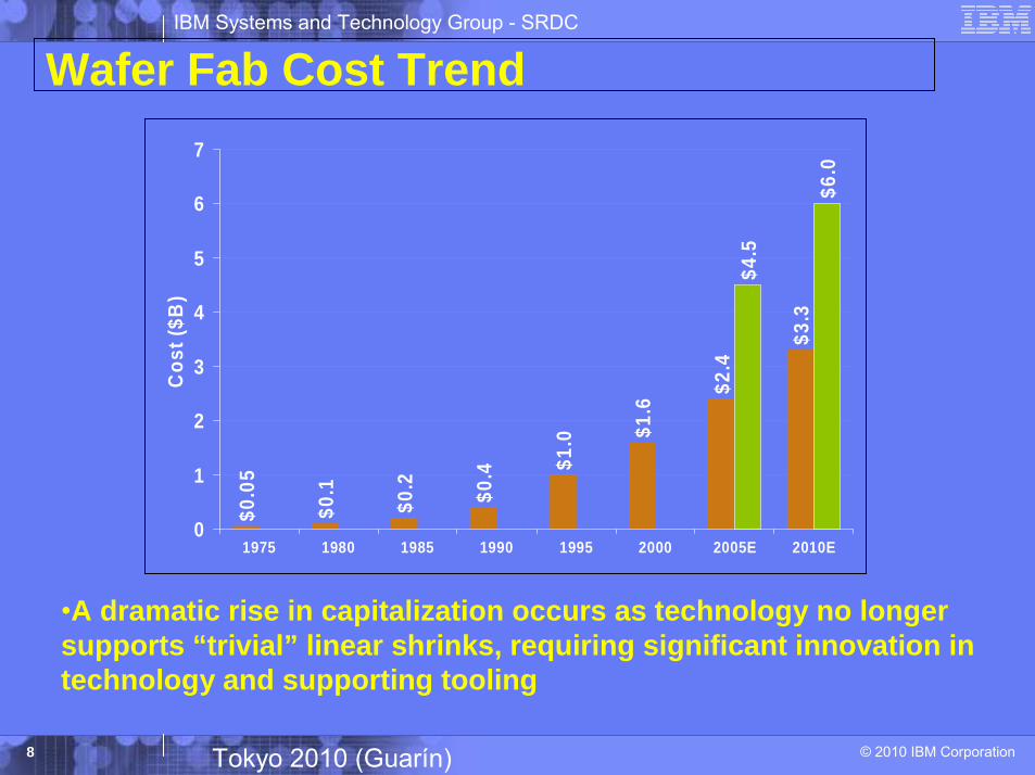
Wafer Fab Cost Trend
$0.1
$0.2 $0
.4 $1.0 $1
.6
$2.4
$3.3
$4.5
$6.0
$0.0
5
0
1
2
3
4
5
6
7
1975 1980 1985 1990 1995 2000 2005E 2010E
Cos
t ($B
)
�A dramatic rise in capitalization occurs as technology no longersupports “trivial” linear shrinks, requiring significant innovation in technology and supporting tooling
IBM Systems and Technology Group - SRDC
© 2010 IBM Corporation9 Tokyo 2010 (Guarín)
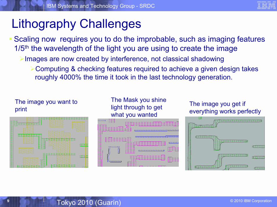
Lithography Challenges! Scaling now requires you to do the improbable, such as imaging features
1/5th the wavelength of the light you are using to create the image#Images are now created by interference, not classical shadowing
#Computing & checking features required to achieve a given design takes roughly 4000% the time it took in the last technology generation.
The image you want to print
The image you get if everything works perfectly
The Mask you shine light through to get what you wanted
IBM Systems and Technology Group - SRDC
© 2010 IBM Corporation10 Tokyo 2010 (Guarín)
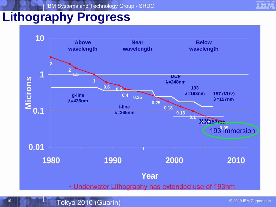
Lithography Progress
32
1.51
0.4 0.350.25
0.180.13
0.10.07
0.05
0.50.6
0.01
0.1
1
10
1980 1990 2000 2010
Year
Mic
rons
Abovewavelength
Nearwavelength
Belowwavelength
g-lineλλλλ=436nm
i-lineλλλλ=365nm
DUVλλλλ=248nm
193λλλλ=193nm 157 (VUV)
λλλλ=157nm
193 immersionXX157nm
� Underwater Lithography has extended use of 193nm
IBM Systems and Technology Group - SRDC
© 2010 IBM Corporation11 Tokyo 2010 (Guarín)
01234567
0 100 200 300 400
technology node (nm)
core
gat
e ox
ide
phys
ical
th
ickn
ess
(nm
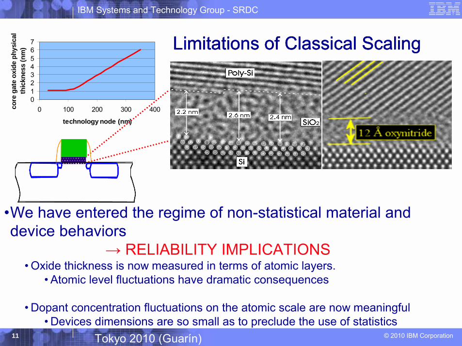
) Limitations of Classical Scaling
�We have entered the regime of non-statistical material and device behaviors
→ RELIABILITY IMPLICATIONS� Oxide thickness is now measured in terms of atomic layers.
� Atomic level fluctuations have dramatic consequences
� Dopant concentration fluctuations on the atomic scale are now meaningful� Devices dimensions are so small as to preclude the use of statistics
Limitations of Classical ScalingLimitations of Classical Scaling
IBM Systems and Technology Group - SRDC
© 2010 IBM Corporation12 Tokyo 2010 (Guarín)
1 Resolution
where sinθ
kNA
NA n
λ=
=
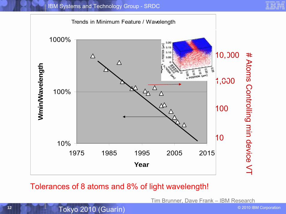
Trends in Minimum Feature / Wavelength
10%
100%
1000%
1975 1985 1995 2005 2015
Year
Wm
in/W
avel
engt
h
10,000
1,000
100
10
# Atom
s Controlling m
in device VT
Tim Brunner, Dave Frank � IBM Research
Tolerances of 8 atoms and 8% of light wavelength!
IBM Systems and Technology Group - SRDC
© 2010 IBM Corporation13 Tokyo 2010 (Guarín)
Challenges and Future Technology Path Reliability Topics
IBM Systems and Technology Group - SRDC
© 2010 IBM Corporation14 Tokyo 2010 (Guarín)
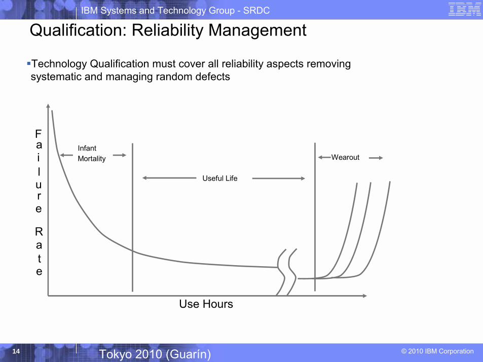
Qualification: Reliability Management
!Technology Qualification must cover all reliability aspects removing systematic and managing random defects
Use Hours
Failure
Rate
Useful Life
InfantMortality Wearout
IBM Systems and Technology Group - SRDC
© 2010 IBM Corporation15 Tokyo 2010 (Guarín)
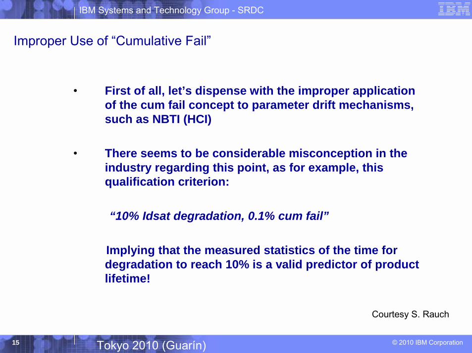
Improper Use of �Cumulative Fail�
� First of all, let’s dispense with the improper application of the cum fail concept to parameter drift mechanisms, such as NBTI (HCI)
� There seems to be considerable misconception in the industry regarding this point, as for example, this qualification criterion:
“10% Idsat degradation, 0.1% cum fail”
Implying that the measured statistics of the time for degradation to reach 10% is a valid predictor of product lifetime!
Courtesy S. Rauch
IBM Systems and Technology Group - SRDC
© 2010 IBM Corporation16 Tokyo 2010 (Guarín)
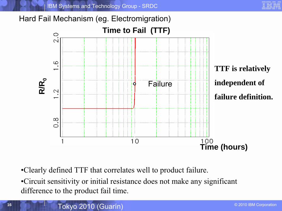
Hard Fail Mechanism (eg. Electromigration)
R/R
0
Time (hours)
Time to Fail (TTF)
Failure
�Clearly defined TTF that correlates well to product failure. �Circuit sensitivity or initial resistance does not make any significant difference to the product fail time.
TTF is relatively
independent of
failure definition.
IBM Systems and Technology Group - SRDC
© 2010 IBM Corporation17 Tokyo 2010 (Guarín)
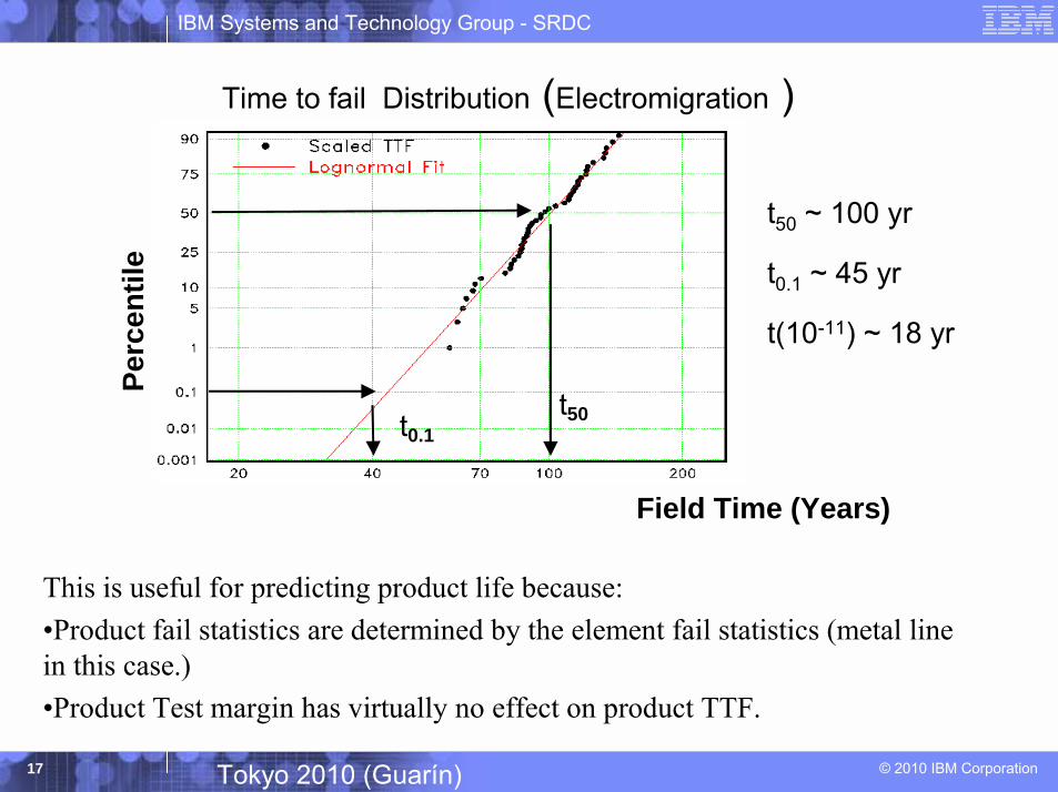
Time to fail Distribution (Electromigration )
This is useful for predicting product life because:�Product fail statistics are determined by the element fail statistics (metal line in this case.)�Product Test margin has virtually no effect on product TTF.
Field Time (Years)
t50 ~ 100 yr
t0.1 ~ 45 yr
t(10-11) ~ 18 yr
Perc
entil
e
t50t0.1
IBM Systems and Technology Group - SRDC
© 2010 IBM Corporation18 Tokyo 2010 (Guarín)
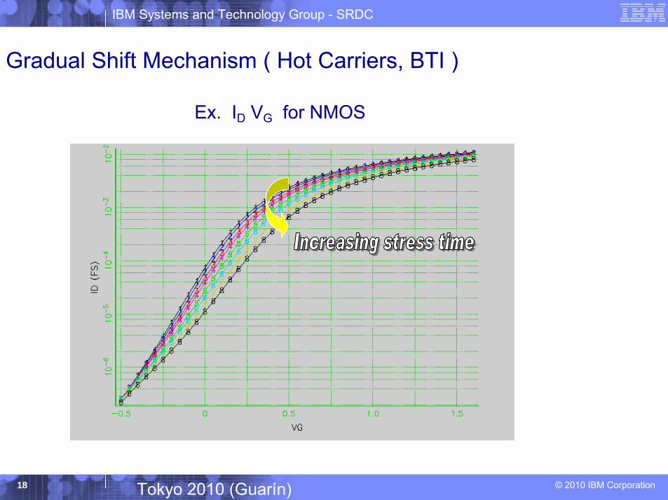
Gradual Shift Mechanism ( Hot Carriers, BTI )
Ex. ID VG for NMOS
IBM Systems and Technology Group - SRDC
© 2010 IBM Corporation19 Tokyo 2010 (Guarín)
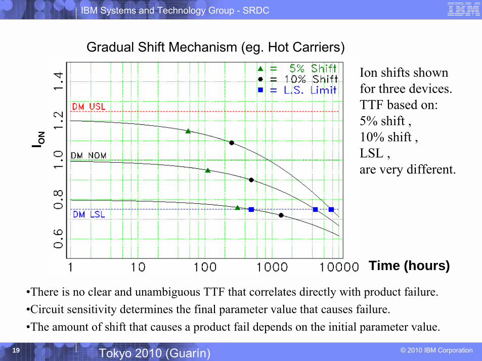
Gradual Shift Mechanism (eg. Hot Carriers)I O
N
Time (hours)
�There is no clear and unambiguous TTF that correlates directly with product failure.�Circuit sensitivity determines the final parameter value that causes failure. �The amount of shift that causes a product fail depends on the initial parameter value.
Ion shifts shownfor three devices. TTF based on:5% shift ,10% shift , LSL ,are very different.
IBM Systems and Technology Group - SRDC
© 2010 IBM Corporation20 Tokyo 2010 (Guarín)
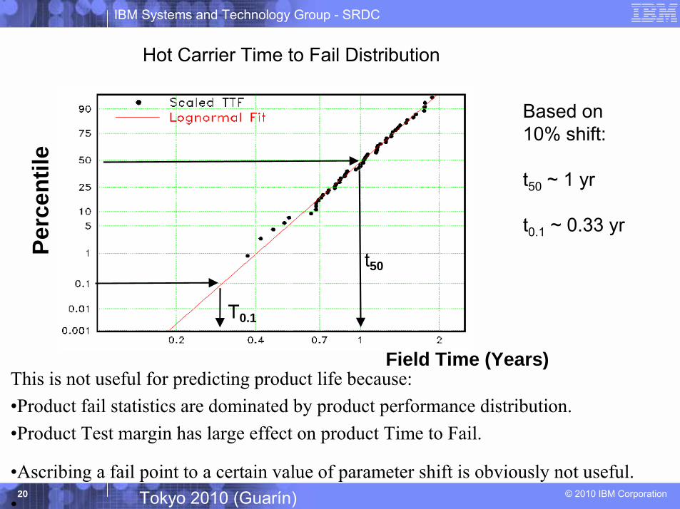
Hot Carrier Time to Fail Distribution
This is not useful for predicting product life because:�Product fail statistics are dominated by product performance distribution.�Product Test margin has large effect on product Time to Fail.
�Ascribing a fail point to a certain value of parameter shift is obviously not useful.
�
Based on10% shift:
t50 ~ 1 yr
t0.1 ~ 0.33 yr
Perc
entil
e
Field Time (Years)
t50
T0.1
IBM Systems and Technology Group - SRDC
© 2010 IBM Corporation21 Tokyo 2010 (Guarín)
Modeling Realistic Impact to Product
! Model device shifts as a function of device parameters (Lpoly, VT, tOX, etc.) and environment (VDD, TJ)
! Model circuit sensitivity (performance shift vs. device shift.)
! Model product performance before and after degradations, taking into account testing strategy. All device shifts must be considered together (NBTI + HC.)
! A robust strategy for model validation must be in place
IBM Systems and Technology Group - SRDC
© 2010 IBM Corporation22 Tokyo 2010 (Guarín)
Channel Hot Carriers
Channel carriers whose temperature (Thc) is locally (near drain) larger than the lattice temperature.
Thc is mainly determined by:Large lateral Electric Field in the pinch-off region.Energy exchange processes (e.g., phonon scattering,
impact ionization, e-e scattering, etc.)

IBM Systems and Technology Group - SRDC
© 2010 IBM Corporation23 Tokyo 2010 (Guarín)
Bad Effects of Channel Hot Carriers
! Carriers with Energy > EG cause Impact Ionization(electron-hole pair generation)Latchup
! Carriers with high Energy impacting the SiO2 interface cause Interface State GenerationION, VT degradation
! Carriers injected into the SiO2 lead to Charge TrappingVT shift
SLOWER CIRCUIT OPERATION
IBM Systems and Technology Group - SRDC
© 2010 IBM Corporation24 Tokyo 2010 (Guarín)
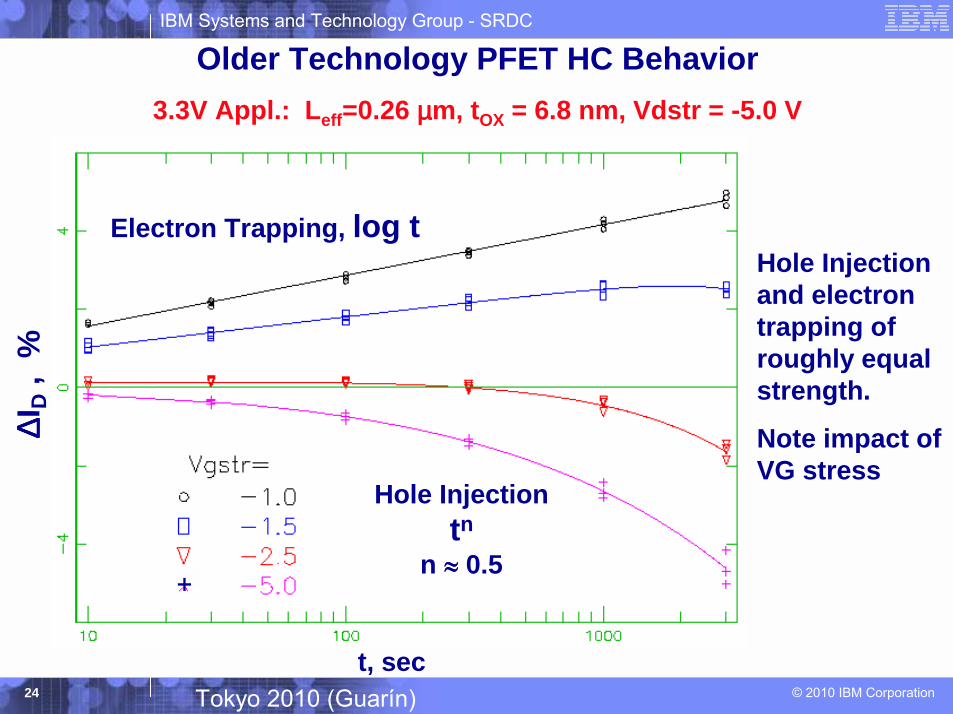
Older Technology PFET HC Behavior3.3V Appl.: Leff=0.26 µµµµm, tOX = 6.8 nm, Vdstr = -5.0 V
∆∆ ∆∆ ID
, %
t, sec
Hole Injection and electron trapping of roughly equal strength.
Note impact of VG stress
Electron Trapping, log t
Hole Injectiontn
n llll 0.5+
IBM Systems and Technology Group - SRDC
© 2010 IBM Corporation25 Tokyo 2010 (Guarín)
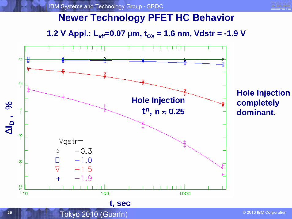
Newer Technology PFET HC Behavior1.2 V Appl.: Leff=0.07 µµµµm, tOX = 1.6 nm, Vdstr = -1.9 V
∆∆ ∆∆ ID
, %
t, sec
Hole Injection completely dominant.
Hole Injectiontn, n llll 0.25
+
IBM Systems and Technology Group - SRDC
© 2010 IBM Corporation26 Tokyo 2010 (Guarín)
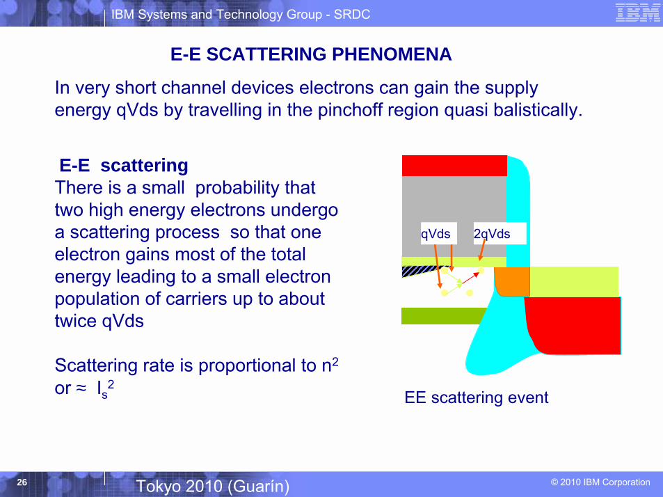
E-E scattering There is a small probability that two high energy electrons undergo a scattering process so that one electron gains most of the total energy leading to a small electron population of carriers up to about twice qVds
Scattering rate is proportional to n2
or ≈ Is2
E-E SCATTERING PHENOMENA
In very short channel devices electrons can gain the supply energy qVds by travelling in the pinchoff region quasi balistically.
qVds 2qVds
EE scattering event
IBM Systems and Technology Group - SRDC
© 2010 IBM Corporation27 Tokyo 2010 (Guarín)
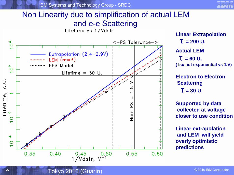
Non Linearity due to simplification of actual LEMand e-e Scattering
Linear Extrapolationττττ = 200 U.
Actual LEM ττττ = 60 U.
( Isx not exponential vs 1/V)
Electron to ElectronScatteringττττ = 30 U.
Supported by datacollected at voltage
closer to use condition
Linear extrapolationand LEM will yield
overly optimistic predictions
IBM Systems and Technology Group - SRDC
© 2010 IBM Corporation28 Tokyo 2010 (Guarín)
BiasTemperature Instability
NBTI - PBTI
IBM Systems and Technology Group - SRDC
© 2010 IBM Corporation29 Tokyo 2010 (Guarín)
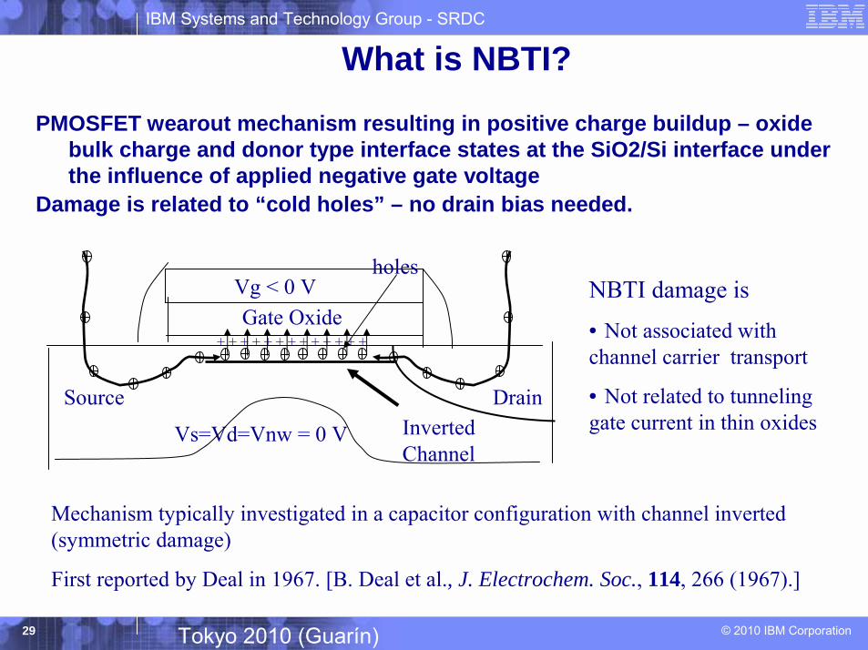
PMOSFET wearout mechanism resulting in positive charge buildup – oxide bulk charge and donor type interface states at the SiO2/Si interface under the influence of applied negative gate voltage
Damage is related to “cold holes” – no drain bias needed.
What is NBTI?
Gate OxideVg < 0 V
Vs=Vd=Vnw = 0 V
holes
Inverted Channel
DrainSource
+ + + + + + + + + + + + +
NBTI damage is
• Not associated with channel carrier transport
• Not related to tunneling gate current in thin oxides
Mechanism typically investigated in a capacitor configuration with channel inverted (symmetric damage)
First reported by Deal in 1967. [B. Deal et al., J. Electrochem. Soc., 114, 266 (1967).]
IBM Systems and Technology Group - SRDC
© 2010 IBM Corporation30 Tokyo 2010 (Guarín)
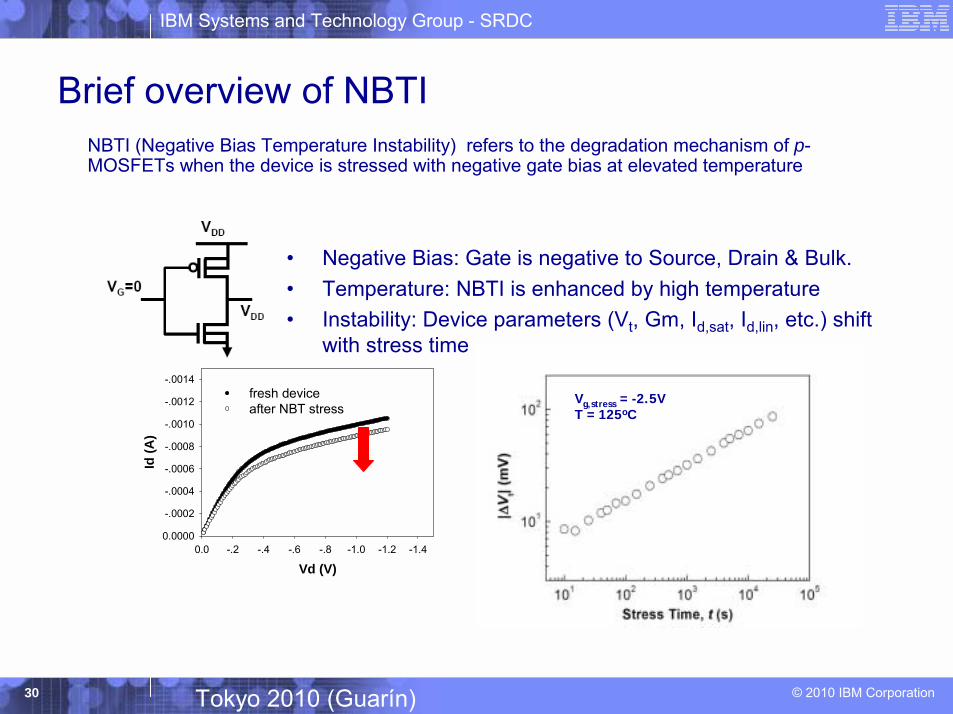
Brief overview of NBTI NBTI (Negative Bias Temperature Instability) refers to the degradation mechanism of p-MOSFETs when the device is stressed with negative gate bias at elevated temperature
� Negative Bias: Gate is negative to Source, Drain & Bulk. � Temperature: NBTI is enhanced by high temperature� Instability: Device parameters (Vt, Gm, Id,sat, Id,lin, etc.) shift
with stress time
Vd (V)-1.4-1.2-1.0-.8-.6-.4-.20.0
Id (A
)
-.0014
-.0012
-.0010
-.0008
-.0006
-.0004
-.0002
0.0000
fresh deviceafter NBT stress
Vg,stress = -2.5VT = 125oC
IBM Systems and Technology Group - SRDC
© 2010 IBM Corporation31 Tokyo 2010 (Guarín)
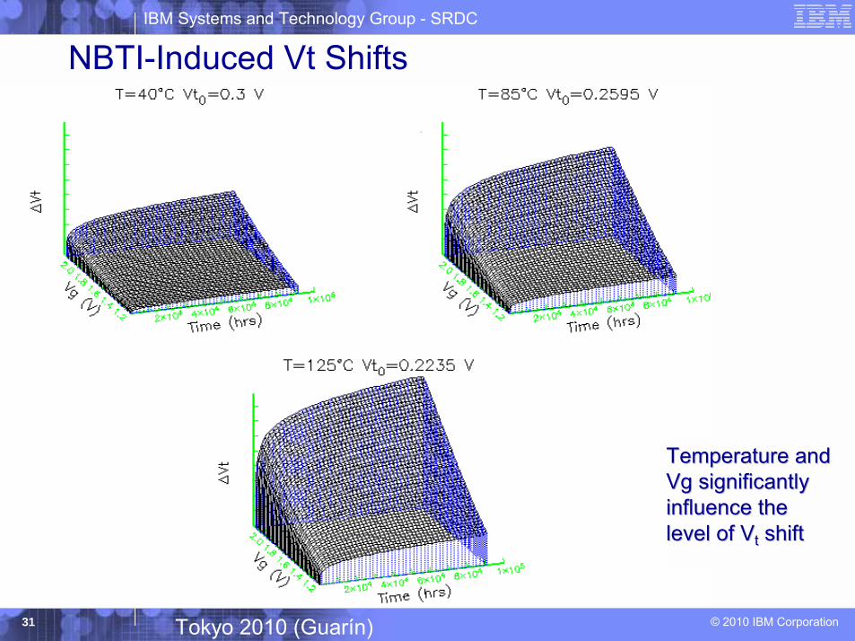
NBTI-Induced Vt Shifts
Temperature and Temperature and Vg significantly Vg significantly influence the influence the level of Vlevel of Vtt shiftshift
IBM Systems and Technology Group - SRDC
© 2010 IBM Corporation32 Tokyo 2010 (Guarín)
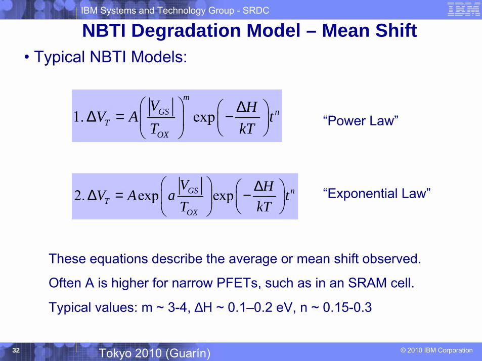
� Typical NBTI Models:NBTI Degradation Model – Mean Shift
1. expm
GS nT
OX
V HV A tT kT
∆ ∆ = −
2. exp expGS nT
OX
V HV A a tT kT
∆ ∆ = −
�Power Law�
�Exponential Law�
These equations describe the average or mean shift observed.
Often A is higher for narrow PFETs, such as in an SRAM cell.
Typical values: m ~ 3-4, ∆H ~ 0.1�0.2 eV, n ~ 0.15-0.3
IBM Systems and Technology Group - SRDC
© 2010 IBM Corporation33 Tokyo 2010 (Guarín)
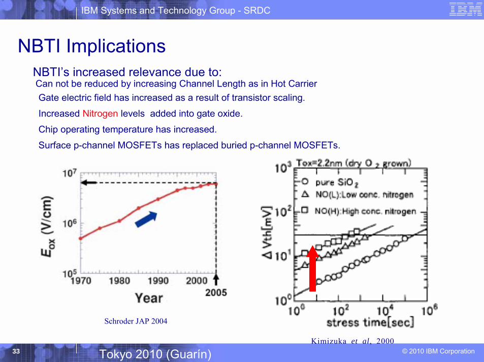
NBTI ImplicationsNBTI�s increased relevance due to:Can not be reduced by increasing Channel Length as in Hot CarrierGate electric field has increased as a result of transistor scaling.
Increased Nitrogen levels added into gate oxide.
Chip operating temperature has increased.
Surface p-channel MOSFETs has replaced buried p-channel MOSFETs.
Schroder JAP 2004
Kimizuka et al, 2000
IBM Systems and Technology Group - SRDC
© 2010 IBM Corporation34 Tokyo 2010 (Guarín)
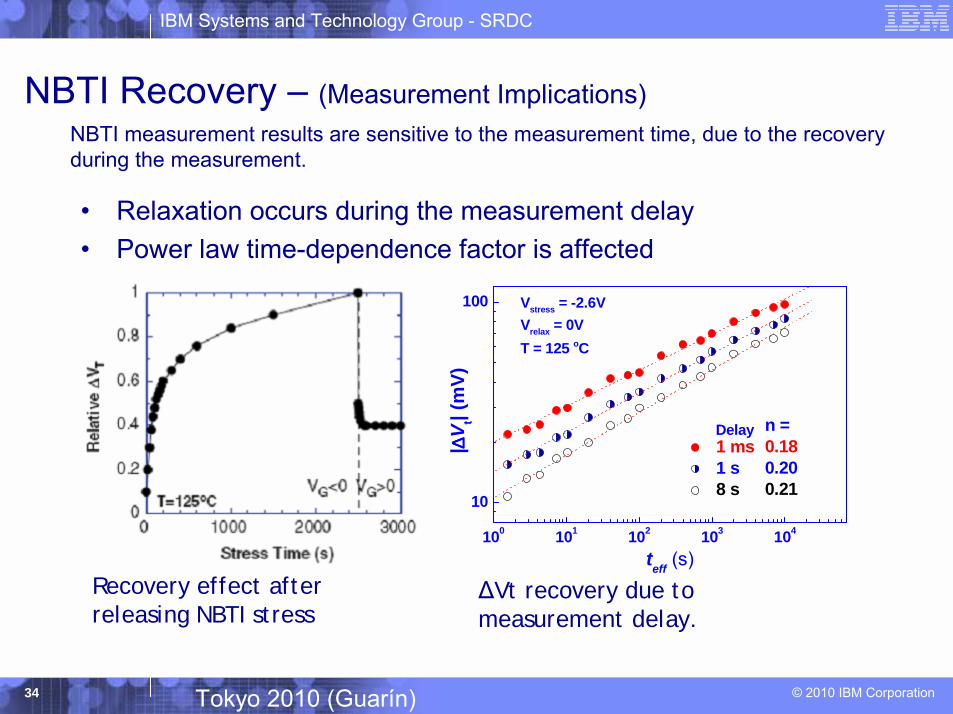
NBTI Recovery � (Measurement Implications)NBTI measurement results are sensitive to the measurement time, due to the recovery during the measurement.
100 101 102 103 104
10
100 Vstress = -2.6VVrelax = 0VT = 125 oC
| ∆∆ ∆∆V t| (
mV)
teff (s)
1 ms 1 s 8 s
n =0.180.200.21
Delay
∆Vt recovery due to measurement delay.
� Relaxation occurs during the measurement delay� Power law time-dependence factor is affected
Recovery effect after releasing NBTI stress
IBM Systems and Technology Group - SRDC
© 2010 IBM Corporation35 Tokyo 2010 (Guarín)
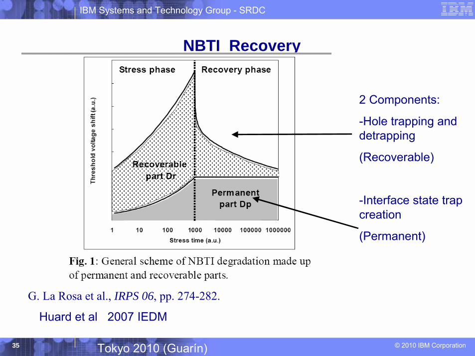
NBTI Recovery
G. La Rosa et al., IRPS 06, pp. 274-282.
2 Components:
-Hole trapping and detrapping
(Recoverable)
-Interface state trap creation
(Permanent)
Huard et al 2007 IEDM
IBM Systems and Technology Group - SRDC
© 2010 IBM Corporation36 Tokyo 2010 (Guarín)
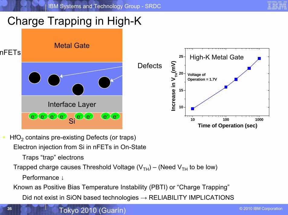
Charge Trapping in High-K
! HfO2 contains pre-existing Defects (or traps)Electron injection from Si in nFETs in On-State
Traps �trap� electronsTrapped charge causes Threshold Voltage (VTH) � (Need VTH to be low)
Performance ↓Known as Positive Bias Temperature Instability (PBTI) or �Charge Trapping�
Did not exist in SiON based technologies → RELIABILITY IMPLICATIONS
10 100 1000
10
15
20
25
Incr
ease
in V
TH(m
V)
Time of Operation (sec)
High-K Metal Gate
Voltage of Operation = 1.7V
Si
Metal GatenFETs
Interface Layer
Defects
e- e- e- e- e- e-e- e-
IBM Systems and Technology Group - SRDC
© 2010 IBM Corporation37 Tokyo 2010 (Guarín)
AC Considerations

IBM Systems and Technology Group - SRDC
© 2010 IBM Corporation38 Tokyo 2010 (Guarín)
Typical Voltage vs. Time plot generated from PowerSPICE for inverter
PDELAYRPDELAYF
VINVOUT
50% VDD
IBM Systems and Technology Group - SRDC
© 2010 IBM Corporation39 Tokyo 2010 (Guarín)
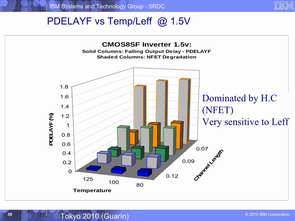
PDELAYF vs Temp/Leff @ 1.5V
80100125 0.12
0.09
0.07
0
0.2
0.4
0.6
0.8
1
1.2
1.4
1.6
1.8
PDEL
AYF
(%)
TemperatureCha
nnel
Leng
th
CMOS8SF Inverter 1.5v:Solid Columns: Falling Output Delay - PDELAYF
Shaded Columns: NFET Degradation
Dominated by H.C(NFET)Very sensitive to Leff
IBM Systems and Technology Group - SRDC
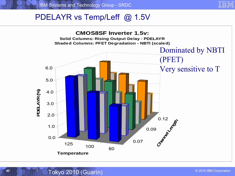
© 2010 IBM Corporation40 Tokyo 2010 (Guarín)
80100125 0.07
0.09
0.12
0.0
1.0
2.0
3.0
4.0
5.0
6.0
PDEL
AYR
(%)
TemperatureCh
anne
l Len
gth
CMOS8SF Inverter 1.5v: Solid Columns: Rising Output Delay - PDELAYR
Shaded Columns: PFET Degradation - NBTI (scaled)
PDELAYR vs Temp/Leff @ 1.5V
Dominated by NBTI(PFET)Very sensitive to T
IBM Systems and Technology Group - SRDC
© 2010 IBM Corporation41 Tokyo 2010 (Guarín)
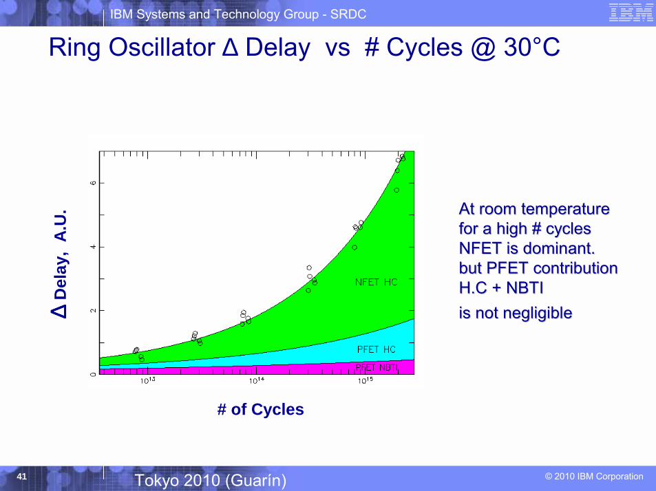
Ring Oscillator ∆ Delay vs # Cycles @ 30°C
At room temperatureAt room temperaturefor a high # cycles for a high # cycles NFET is dominant.NFET is dominant.but PFET contribution but PFET contribution H.C + NBTIH.C + NBTIis not negligibleis not negligible∆∆ ∆∆
Del
ay,
A.U
.
# of Cycles
IBM Systems and Technology Group - SRDC
© 2010 IBM Corporation42 Tokyo 2010 (Guarín)
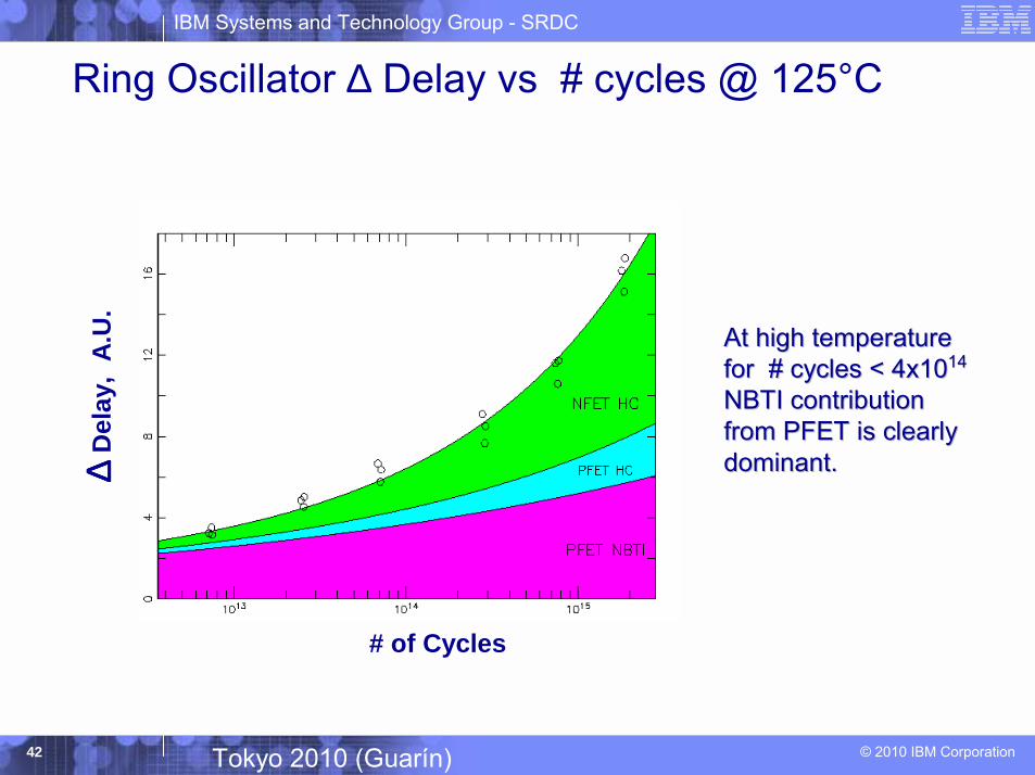
Ring Oscillator ∆ Delay vs # cycles @ 125°C
At high temperatureAt high temperaturefor # cycles < 4x10for # cycles < 4x101414
NBTI contribution NBTI contribution from PFET is clearly from PFET is clearly dominant.dominant.∆∆ ∆∆
Del
ay,
A.U
.
# of Cycles
IBM Systems and Technology Group - SRDC
© 2010 IBM Corporation43 Tokyo 2010 (Guarín)
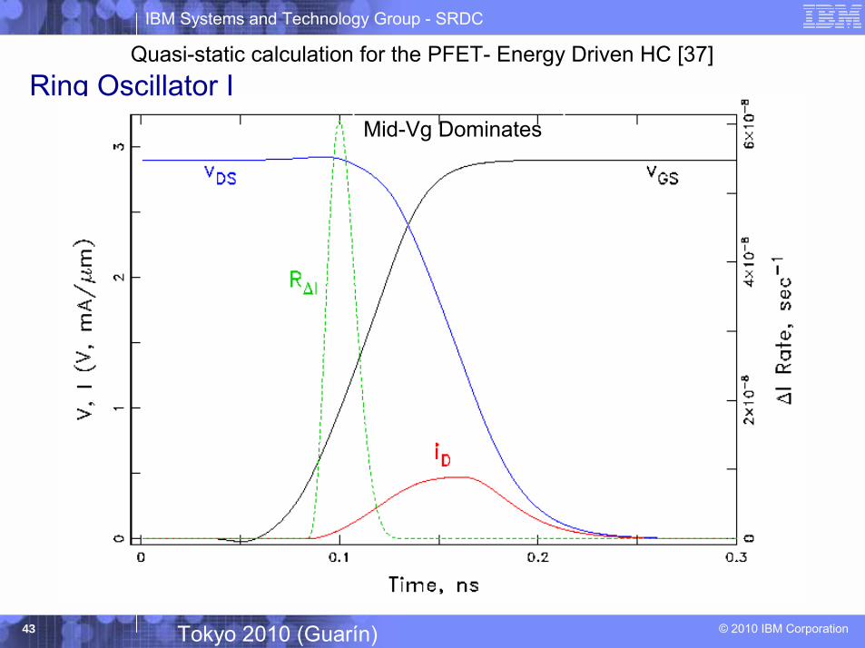
Ring Oscillator IQuasi-static calculation for the PFET- Energy Driven HC [37]
Mid-Vg Dominates
IBM Systems and Technology Group - SRDC
© 2010 IBM Corporation44 Tokyo 2010 (Guarín)
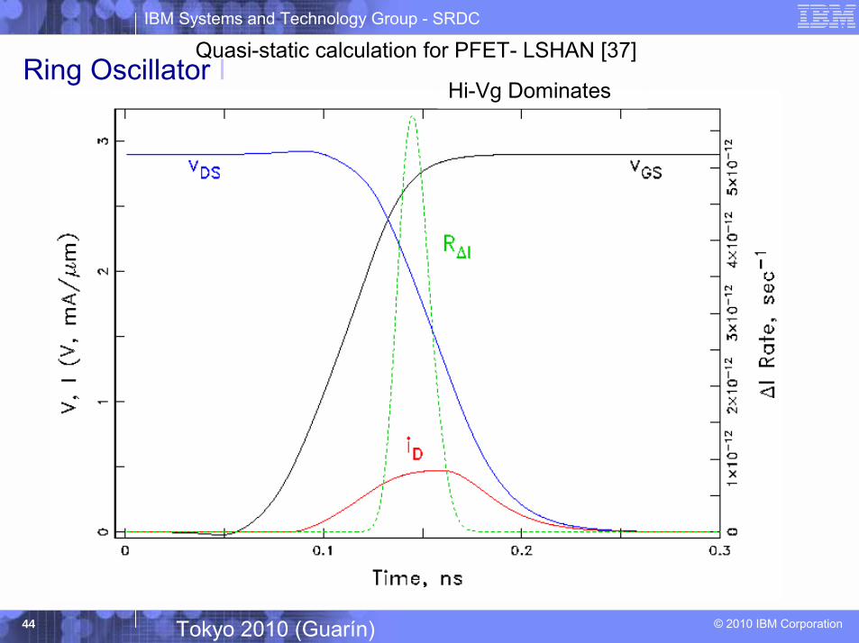
Ring Oscillator I Quasi-static calculation for PFET- LSHAN [37]
Hi-Vg Dominates
IBM Systems and Technology Group - SRDC
© 2010 IBM Corporation45 Tokyo 2010 (Guarín)
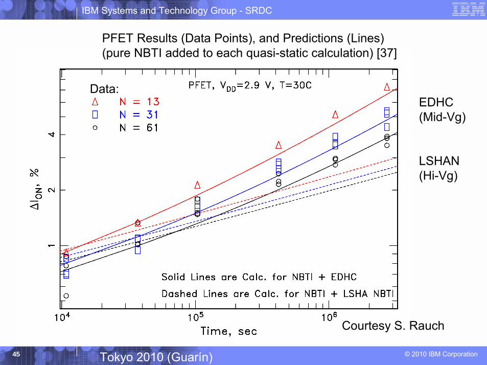
PFET Results (Data Points), and Predictions (Lines)(pure NBTI added to each quasi-static calculation) [37]
EDHC(Mid-Vg)
LSHAN(Hi-Vg)
Data:
Courtesy S. Rauch
IBM Systems and Technology Group - SRDC
© 2010 IBM Corporation46 Tokyo 2010 (Guarín)
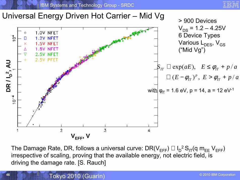
Universal Energy Driven Hot Carrier � Mid VgD
R /
I D2 ,
AU
VEFF, V
> 900 Devices VDS = 1.2 � 4.25V6 Device Types Various LDES, VGS(�Mid Vg�)
The Damage Rate, DR, follows a universal curve: DR(VEFF) ∝ ID2 SIT(q mEE VEFF)irrespective of scaling, proving that the available energy, not electric field, is driving the damage rate. [S. Rauch]
exp( ), /
( ) , /IT IT
pIT IT
S aE E p aE E p a
φφ φ
∝ ≤ +
∝ − > +
with φIT = 1.6 eV, p = 14, a = 12 eV-1
IBM Systems and Technology Group - SRDC
© 2010 IBM Corporation47 Tokyo 2010 (Guarín)
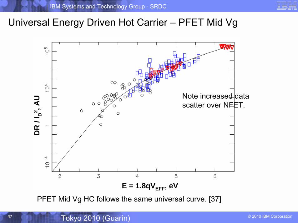
Universal Energy Driven Hot Carrier � PFET Mid Vg
PFET Mid Vg HC follows the same universal curve. [37]
∆DR
/ I D
2 , A
U
E = 1.8qVEFF, eV
Note increased datascatter over NFET.
IBM Systems and Technology Group - SRDC
© 2010 IBM Corporation48 Tokyo 2010 (Guarín)
SRAM Reliability Topics

IBM Systems and Technology Group - SRDC
© 2010 IBM Corporation49 Tokyo 2010 (Guarín)
6 Transistor SRAM bit cell
PU PFET(P0)
PD NFET(N0)
PU PFET(P1)
PD NFET(N1)
PG NFET(T0)
PG NFET(T1)
Vdd
Word Line (WL)
BLT(Bit Line True)
BLC(Bit Line Complement)
Gnd
PG = Pass GateTransfer GateAccess Transistor
PD = Pull Down
PU = Pull Up
IBM Systems and Technology Group - SRDC
© 2010 IBM Corporation50 Tokyo 2010 (Guarín)
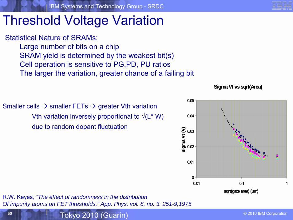
Threshold Voltage Variation
Sigma Vt vs sqrt(Area)
0
0.01
0.02
0.03
0.04
0.05
0.01 0.1 1
sqrt(gate area) (um)si
gma
Vt(V
)
Sigma Vt vs sqrt(Area)
0
0.01
0.02
0.03
0.04
0.05
0.01 0.1 1
sqrt(gate area) (um)si
gma
Vt(V
)
Smaller cells $ smaller FETs $ greater Vth variationVth variation inversely proportional to √(L* W)due to random dopant fluctuation
R.W. Keyes, “The effect of randomness in the distributionOf impurity atoms on FET thresholds,” App. Phys. vol. 8, no. 3: 251-9,1975
Statistical Nature of SRAMs:Large number of bits on a chipSRAM yield is determined by the weakest bit(s)Cell operation is sensitive to PG,PD, PU ratiosThe larger the variation, greater chance of a failing bit
IBM Systems and Technology Group - SRDC
© 2010 IBM Corporation51 Tokyo 2010 (Guarín)
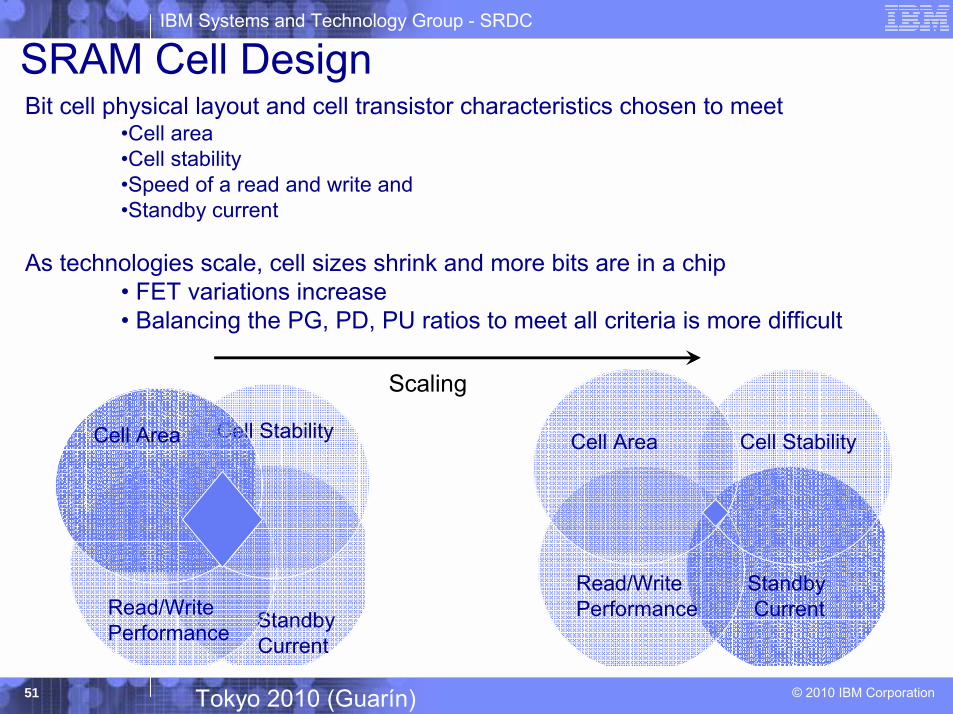
SRAM Cell DesignBit cell physical layout and cell transistor characteristics chosen to meet
�Cell area �Cell stability �Speed of a read and write and �Standby current
As technologies scale, cell sizes shrink and more bits are in a chip� FET variations increase � Balancing the PG, PD, PU ratios to meet all criteria is more difficult
StandbyCurrent
Read/WritePerformance
Cell StabilityCell Area
Technology scaling
Standby Current
Read/WritePerformance
Cell StabilityCell Area
Scaling
IBM Systems and Technology Group - SRDC
© 2010 IBM Corporation52 Tokyo 2010 (Guarín)
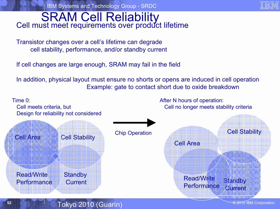
SRAM Cell Reliability
Standby Current
Read/WritePerformance
Cell StabilityCell Area
Cell must meet requirements over product lifetime
Transistor changes over a cell�s lifetime can degrade cell stability, performance, and/or standby current
If cell changes are large enough, SRAM may fail in the field
In addition, physical layout must ensure no shorts or opens are induced in cell operationExample: gate to contact short due to oxide breakdown
Time 0:Cell meets criteria, butDesign for reliability not considered
Chip Operation
After N hours of operation:Cell no longer meets stability criteria
Standby Current
Read/WritePerformance
Cell Stability
Cell Area
IBM Systems and Technology Group - SRDC
© 2010 IBM Corporation53 Tokyo 2010 (Guarín)
SRAM Vmin Failure Mechanism
WL WL
BLT BLC
T1 T2
T3 T4
T5 T6A B
! Gate oxide leakage degrades the pull-down N-FET
! P-FET degrades due to NBTI! P-FET fights to keep high node at VDD
! This mechanism degrades stability of the cell
! Causing Vmin to be out specification
Oxide leakage defect
PFET NBTI
VDD
Mueller et al. IRPS 2004
IBM Systems and Technology Group - SRDC
© 2010 IBM Corporation54 Tokyo 2010 (Guarín)
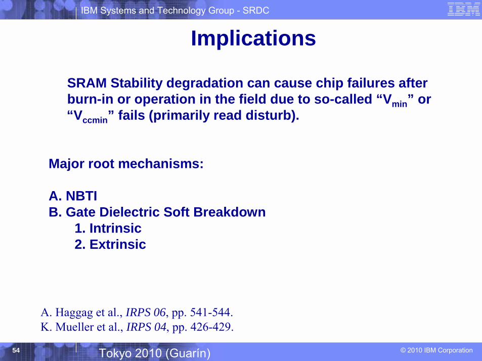
SRAM Stability degradation can cause chip failures afterburn-in or operation in the field due to so-called “Vmin” or “Vccmin” fails (primarily read disturb).
Major root mechanisms:
A. NBTIB. Gate Dielectric Soft Breakdown
1. Intrinsic2. Extrinsic
Implications
A. Haggag et al., IRPS 06, pp. 541-544.K. Mueller et al., IRPS 04, pp. 426-429.
IBM Systems and Technology Group - SRDC
© 2010 IBM Corporation55 Tokyo 2010 (Guarín)
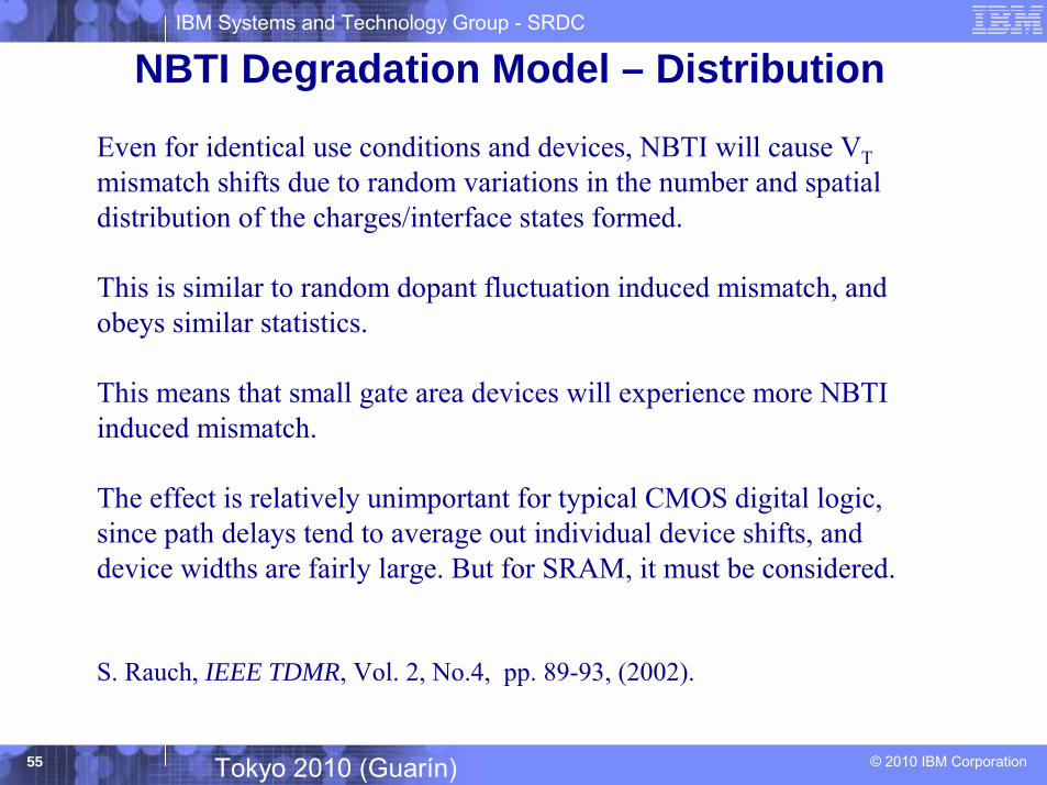
NBTI Degradation Model – Distribution
Even for identical use conditions and devices, NBTI will cause VTmismatch shifts due to random variations in the number and spatial distribution of the charges/interface states formed.
This is similar to random dopant fluctuation induced mismatch, and obeys similar statistics.
This means that small gate area devices will experience more NBTI induced mismatch.
The effect is relatively unimportant for typical CMOS digital logic, since path delays tend to average out individual device shifts, and device widths are fairly large. But for SRAM, it must be considered.
S. Rauch, IEEE TDMR, Vol. 2, No.4, pp. 89-93, (2002).
IBM Systems and Technology Group - SRDC
© 2010 IBM Corporation56 Tokyo 2010 (Guarín)
Review and Perspective
IBM Systems and Technology Group - SRDC
© 2010 IBM Corporation57 Tokyo 2010 (Guarín)
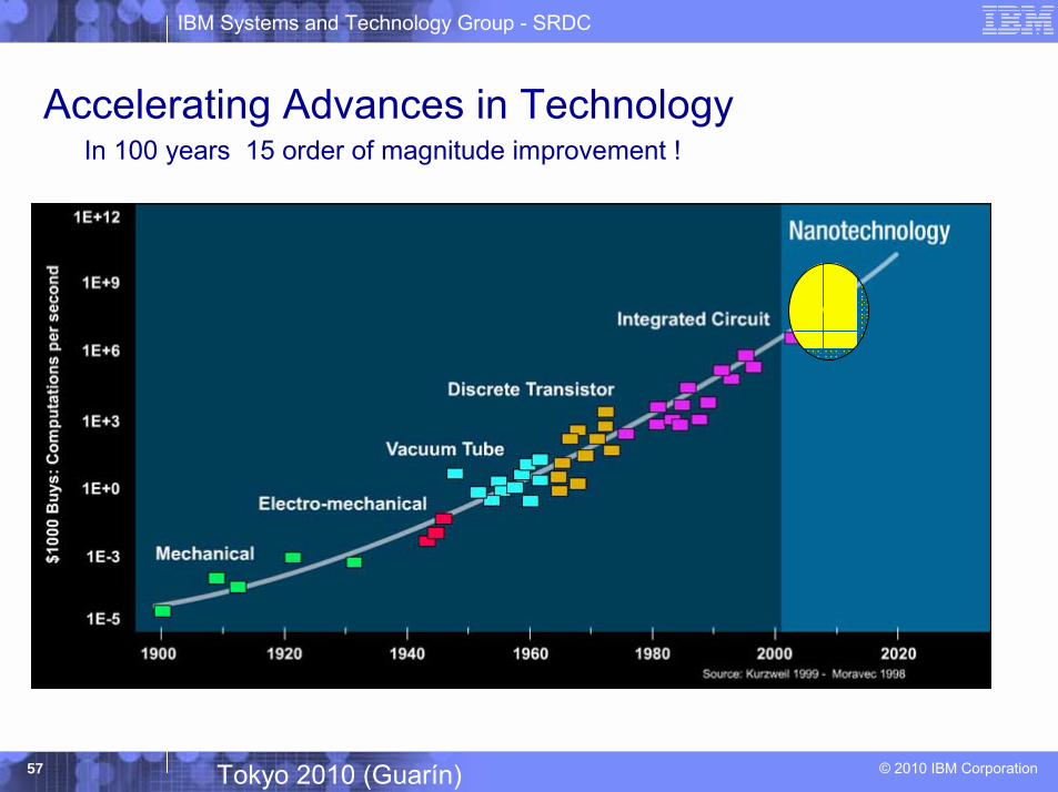
Accelerating Advances in TechnologyIn 100 years 15 order of magnitude improvement !
IBM Systems and Technology Group - SRDC
© 2010 IBM Corporation58 Tokyo 2010 (Guarín)
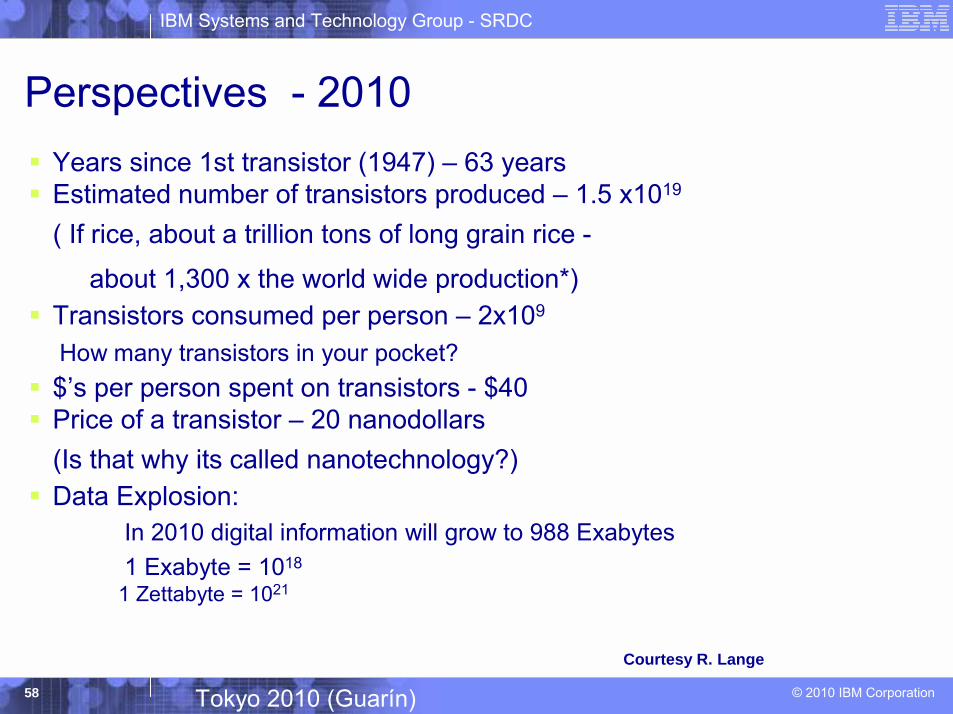
Perspectives - 2010! Years since 1st transistor (1947) � 63 years! Estimated number of transistors produced � 1.5 x10¹⁹
( If rice, about a trillion tons of long grain rice -
about 1,300 x the world wide production*)! Transistors consumed per person � 2x10⁹
How many transistors in your pocket?! $�s per person spent on transistors - $40! Price of a transistor � 20 nanodollars
(Is that why its called nanotechnology?)! Data Explosion:
In 2010 digital information will grow to 988 Exabytes1 Exabyte = 1018
1 Zettabyte = 1021
Courtesy R. Lange
IBM Systems and Technology Group - SRDC
© 2010 IBM Corporation59 Tokyo 2010 (Guarín)
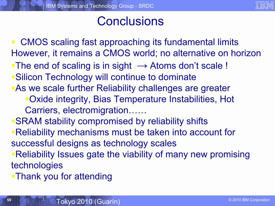
Conclusions! CMOS scaling fast approaching its fundamental limits However, it remains a CMOS world; no alternative on horizon!The end of scaling is in sight → Atoms don�t scale !!Silicon Technology will continue to dominate!As we scale further Reliability challenges are greater
!Oxide integrity, Bias Temperature Instabilities, Hot Carriers, electromigration��
!SRAM stability compromised by reliability shifts !Reliability mechanisms must be taken into account for successful designs as technology scales!Reliability Issues gate the viability of many new promising technologies!Thank you for attending


![Cmos Rf Cituits Sic] Variability And Reliability Resilient ...](https://static.fdocuments.in/doc/165x107/61eff30f1f58b06c3f317164/cmos-rf-cituits-sic-variability-and-reliability-resilient-.jpg)