Semiconductor Optoelectronic Devices · Giovanni Ghione, Semiconductor Devices for High-Speed...
62
Transcript of Semiconductor Optoelectronic Devices · Giovanni Ghione, Semiconductor Devices for High-Speed...
Semiconductor Optoelectronic Devices
Cheng Wang
Phone: 20685263 Office: SIST 401E
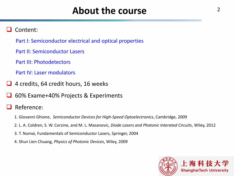
About the course
Content:
Part I: Semiconductor electrical and optical properties
Part II: Semiconductor Lasers
Part III: Photodetectors
Part IV: Laser modulators
4 credits, 64 credit hours, 16 weeks
60% Exame+40% Projects & Experiments
Reference:
1. Giovanni Ghione, Semiconductor Devices for High-Speed Optoelectronics, Cambridge, 2009
2. L. A. Coldren, S. W. Corzine, and M. L. Masanovic, Diode Lasers and Photonic Interated Circuits, Wiley, 2012
3. T. Numai, Fundamentals of Semiconductor Lasers, Springer, 2004
4. Shun Lien Chuang, Physics of Photonic Devices, Wiley, 2009
2
Lecture 1 3
Background: Fiber-optic communications
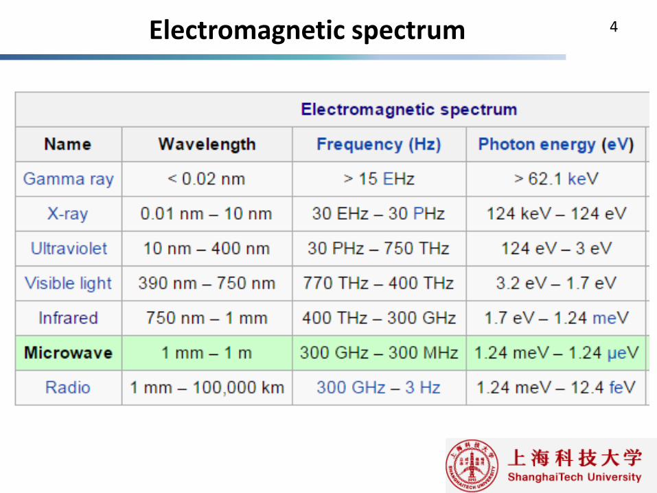
Electromagnetic spectrum 4
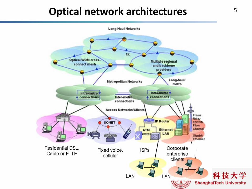
Optical network architectures 5
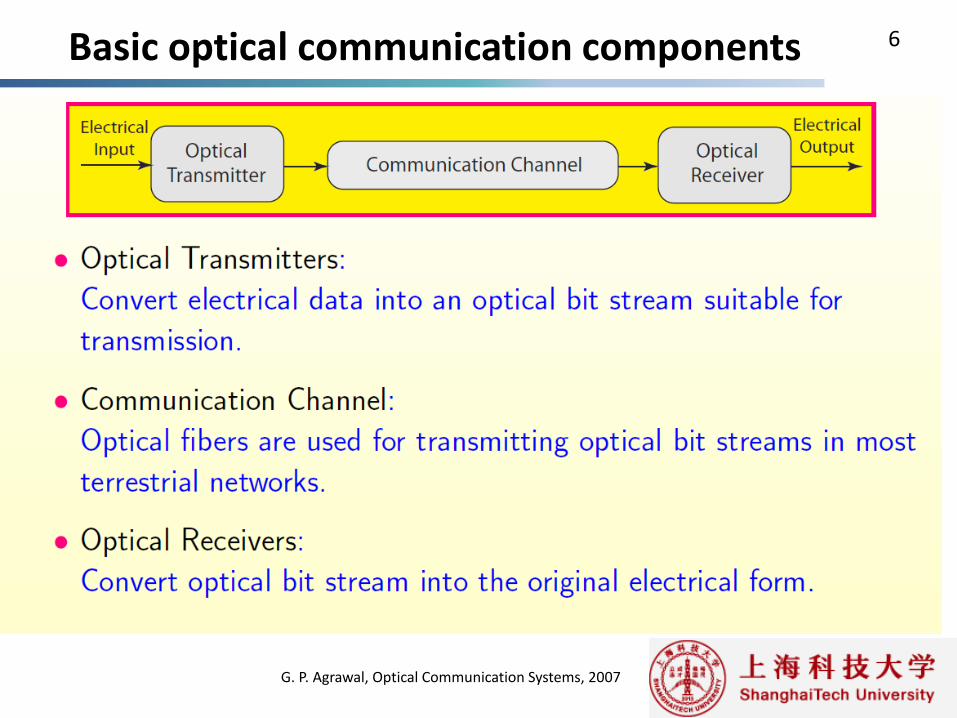
Basic optical communication components 6
G. P. Agrawal, Optical Communication Systems, 2007
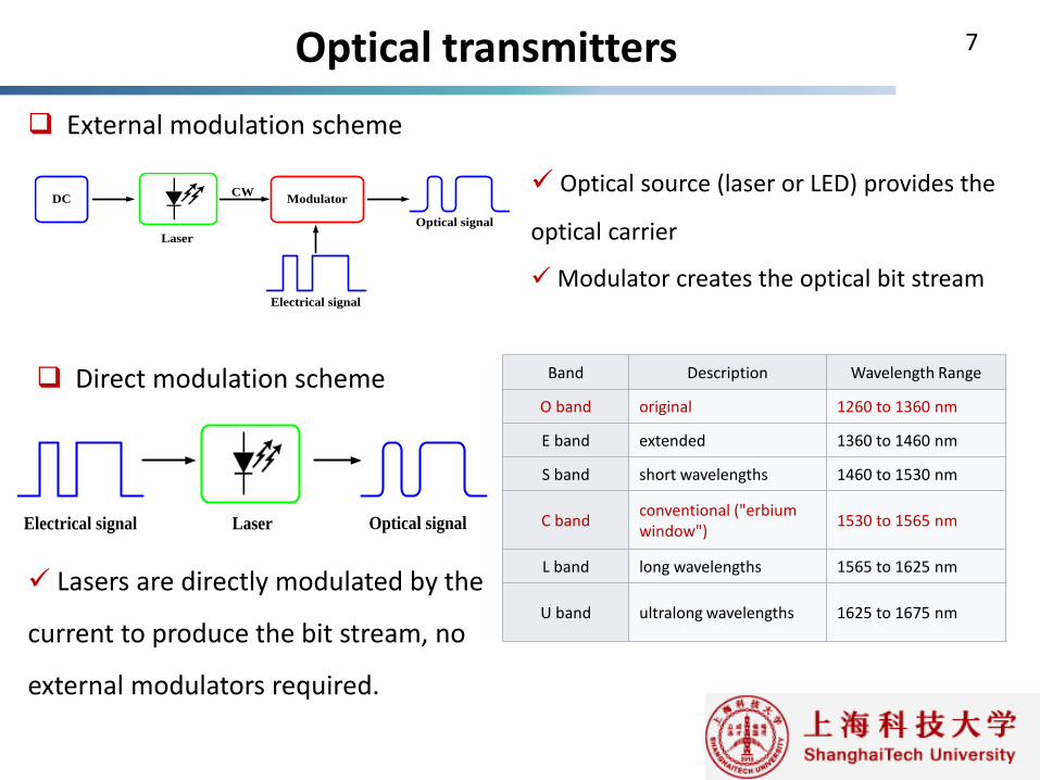
Optical transmitters 7
ModulatorDCCW
Optical signal
Electrical signal
Laser
External modulation scheme
Optical source (laser or LED) provides the
optical carrier
Modulator creates the optical bit stream
Band Description Wavelength Range
O band original 1260 to 1360 nm
E band extended 1360 to 1460 nm
S band short wavelengths 1460 to 1530 nm
C band conventional ("erbium window")
1530 to 1565 nm
L band long wavelengths 1565 to 1625 nm
U band ultralong wavelengths 1625 to 1675 nm
Direct modulation scheme
Electrical signal Optical signalLaser
Lasers are directly modulated by the
current to produce the bit stream, no
external modulators required.
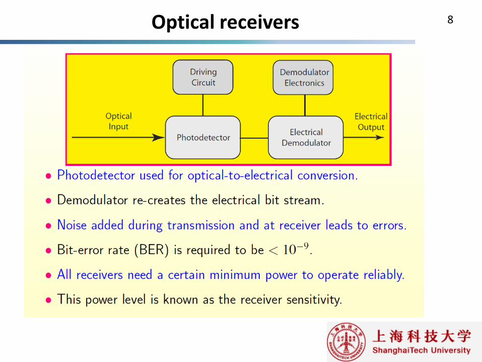
Optical receivers 8
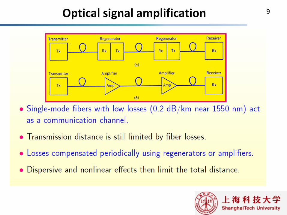
Optical signal amplification 9
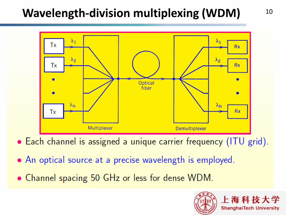
Wavelength-division multiplexing (WDM) 10
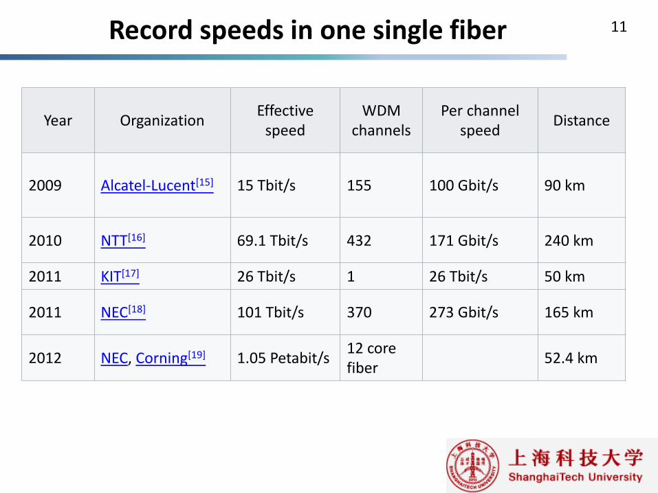
Record speeds in one single fiber 11
Year Organization Effective
speed WDM
channels Per channel
speed Distance
2009 Alcatel-Lucent[15] 15 Tbit/s 155 100 Gbit/s 90 km
2010 NTT[16] 69.1 Tbit/s 432 171 Gbit/s 240 km
2011 KIT[17] 26 Tbit/s 1 26 Tbit/s 50 km
2011 NEC[18] 101 Tbit/s 370 273 Gbit/s 165 km
2012 NEC, Corning[19] 1.05 Petabit/s 12 core fiber
52.4 km
Part I
Semiconductor electrical and optical properties
---- Electrical properties
----Opical properties
Lecture 2 13
Basics of semiconductors
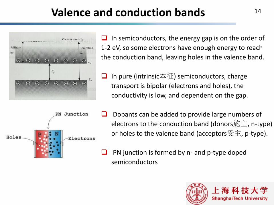
Valence and conduction bands 14
In semiconductors, the energy gap is on the order of
1-2 eV, so some electrons have enough energy to reach
the conduction band, leaving holes in the valence band.
In pure (intrinsic本征) semiconductors, charge
transport is bipolar (electrons and holes), the
conductivity is low, and dependent on the gap.
Dopants can be added to provide large numbers of
electrons to the conduction band (donors施主, n-type)
or holes to the valence band (acceptors受主, p-type).
PN junction is formed by n- and p-type doped
semiconductors
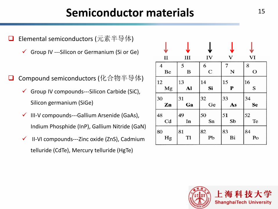
Semiconductor materials 15
Elemental semiconductors (元素半导体)
Group IV ---Silicon or Germanium (Si or Ge)
Compound semiconductors (化合物半导体)
Group IV compounds---Silicon Carbide (SiC),
Silicon germanium (SiGe)
III-V compounds---Gallium Arsenide (GaAs),
Indium Phosphide (InP), Gallium Nitride (GaN)
II-VI compounds---Zinc oxide (ZnS), Cadmium
telluride (CdTe), Mercury telluride (HgTe)
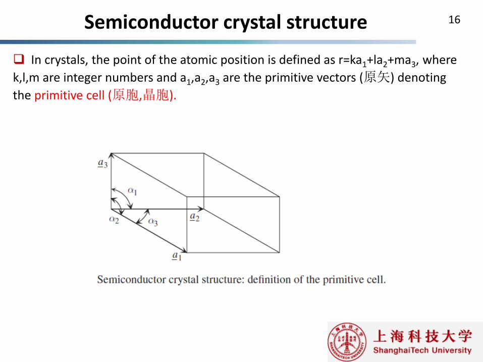
Semiconductor crystal structure 16
In crystals, the point of the atomic position is defined as r=ka1+la2+ma3, where
k,l,m are integer numbers and a1,a2,a3 are the primitive vectors (原矢) denoting
the primitive cell (原胞,晶胞).
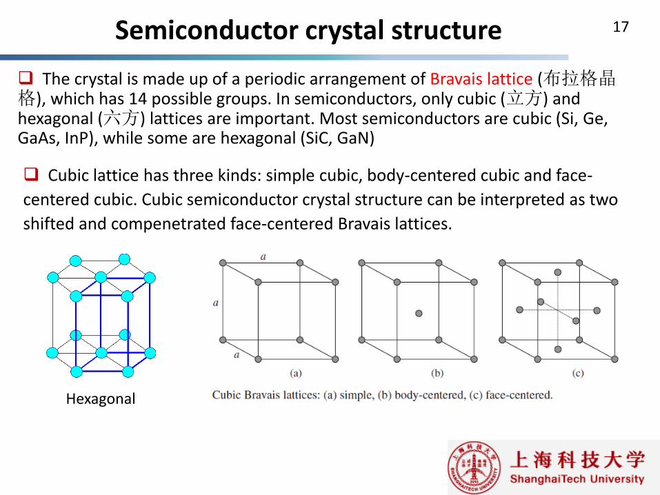
Semiconductor crystal structure 17
The crystal is made up of a periodic arrangement of Bravais lattice (布拉格晶格), which has 14 possible groups. In semiconductors, only cubic (立方) and hexagonal (六方) lattices are important. Most semiconductors are cubic (Si, Ge, GaAs, InP), while some are hexagonal (SiC, GaN)
Cubic lattice has three kinds: simple cubic, body-centered cubic and face-
centered cubic. Cubic semiconductor crystal structure can be interpreted as two
shifted and compenetrated face-centered Bravais lattices.
Hexagonal
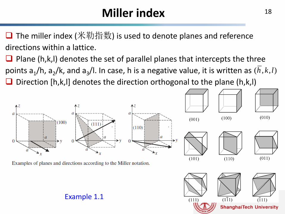
Miller index 18
The miller index (米勒指数) is used to denote planes and reference
directions within a lattice.
Plane (h,k,l) denotes the set of parallel planes that intercepts the three
points a1/h, a2/k, and a3/l. In case, h is a negative value, it is written as
Direction [h,k,l] denotes the direction orthogonal to the plane (h,k,l)
( , , )h k l
Example 1.1
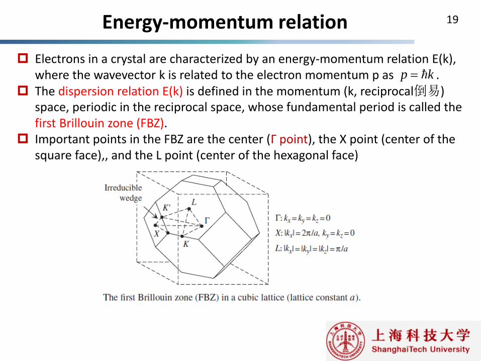
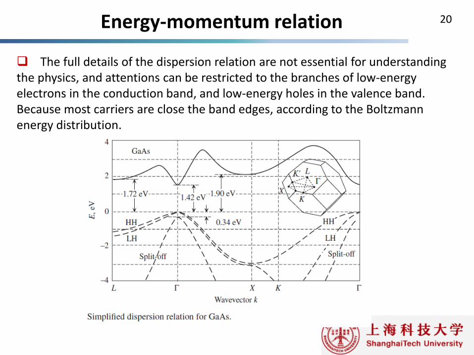
Energy-momentum relation 19
Electrons in a crystal are characterized by an energy-momentum relation E(k), where the wavevector k is related to the electron momentum p as .
The dispersion relation E(k) is defined in the momentum (k, reciprocal倒易) space, periodic in the reciprocal space, whose fundamental period is called the first Brillouin zone (FBZ).
Important points in the FBZ are the center (Г point), the X point (center of the square face),, and the L point (center of the hexagonal face)
p k
Energy-momentum relation 20
The full details of the dispersion relation are not essential for understanding the physics, and attentions can be restricted to the branches of low-energy electrons in the conduction band, and low-energy holes in the valence band. Because most carriers are close the band edges, according to the Boltzmann energy distribution.
Energy-momentum relation 21
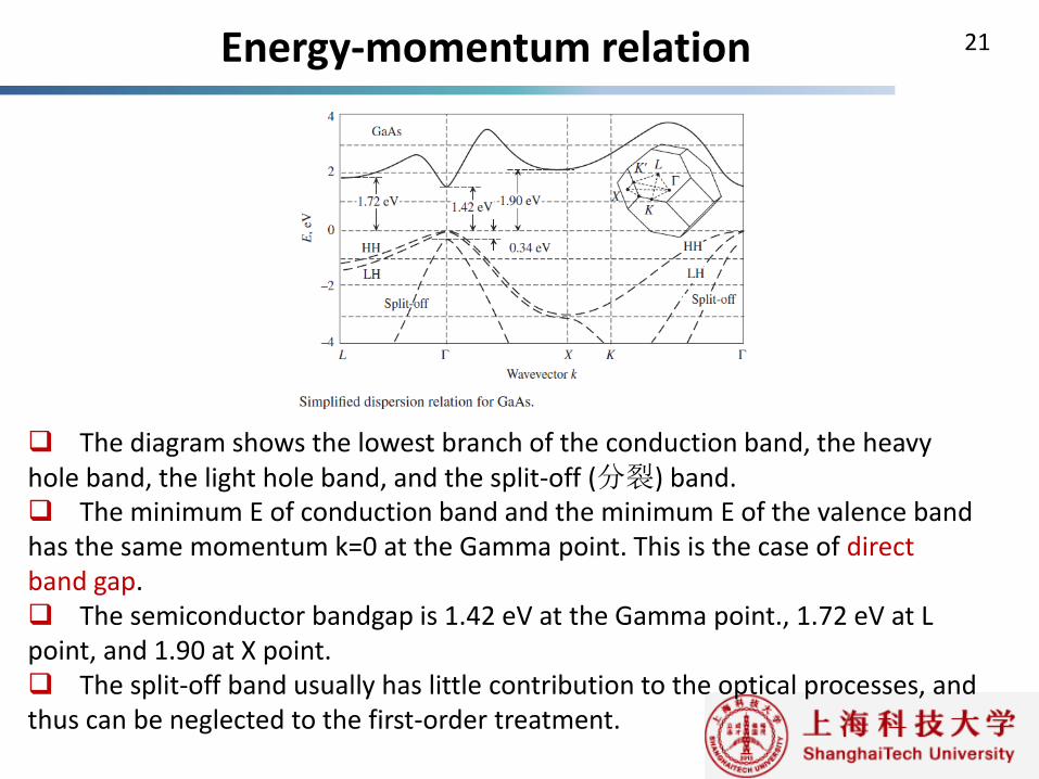
The diagram shows the lowest branch of the conduction band, the heavy hole band, the light hole band, and the split-off (分裂) band. The minimum E of conduction band and the minimum E of the valence band has the same momentum k=0 at the Gamma point. This is the case of direct band gap. The semiconductor bandgap is 1.42 eV at the Gamma point., 1.72 eV at L point, and 1.90 at X point. The split-off band usually has little contribution to the optical processes, and thus can be neglected to the first-order treatment.
Energy-momentum relation 22
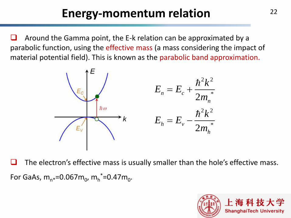
Around the Gamma point, the E-k relation can be approximated by a parabolic function, using the effective mass (a mass considering the impact of material potential field). This is known as the parabolic band approximation.
2 2
*
2 2
*
2
2
n c
n
h v
h
kE E
m
kE E
m
The electron’s effective mass is usually smaller than the hole’s effective mass.
For GaAs, mn*=0.067m0, mh*=0.47m0.
Conduction and valence band wavefunctions 23
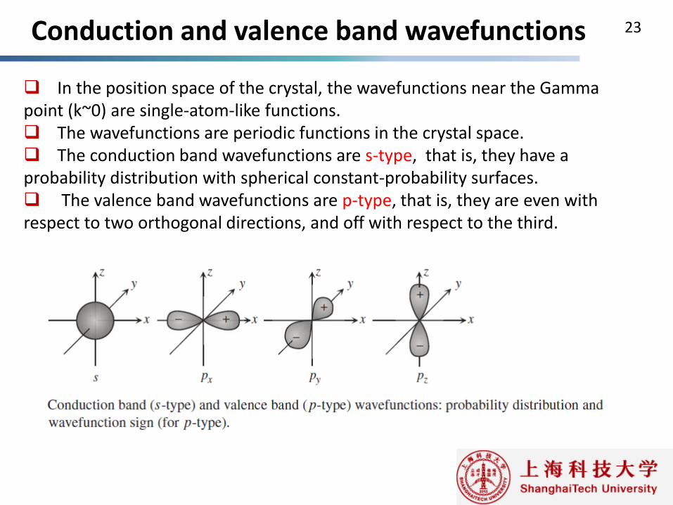
In the position space of the crystal, the wavefunctions near the Gamma point (k~0) are single-atom-like functions. The wavefunctions are periodic functions in the crystal space. The conduction band wavefunctions are s-type, that is, they have a probability distribution with spherical constant-probability surfaces. The valence band wavefunctions are p-type, that is, they are even with respect to two orthogonal directions, and off with respect to the third.
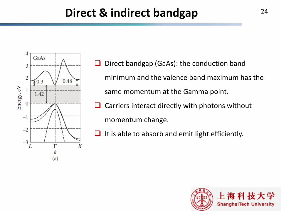
Direct & indirect bandgap 24
Direct bandgap (GaAs): the conduction band
minimum and the valence band maximum has the
same momentum at the Gamma point.
Carriers interact directly with photons without
momentum change.
It is able to absorb and emit light efficiently.
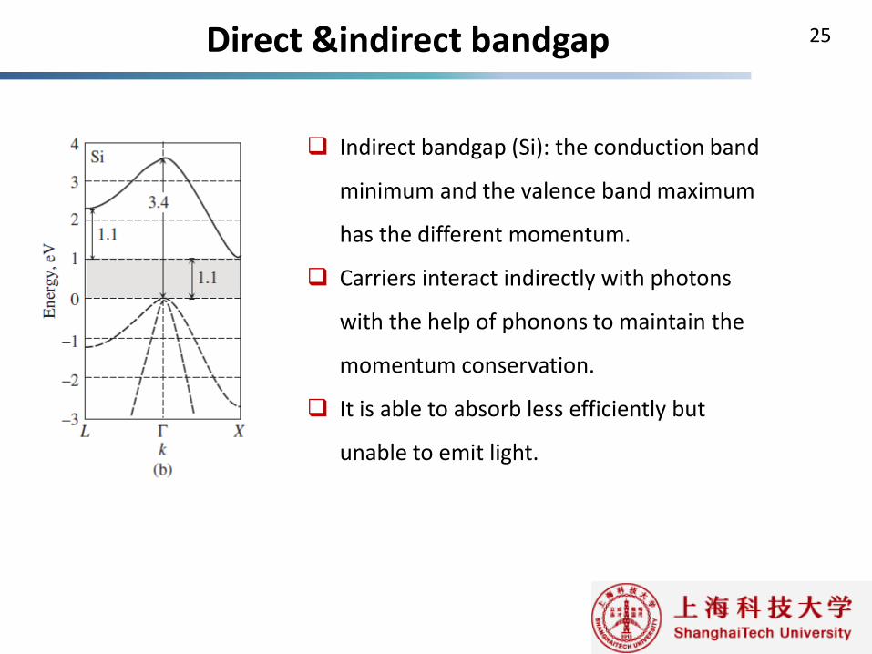
Direct &indirect bandgap 25
Indirect bandgap (Si): the conduction band
minimum and the valence band maximum
has the different momentum.
Carriers interact indirectly with photons
with the help of phonons to maintain the
momentum conservation.
It is able to absorb less efficiently but
unable to emit light.
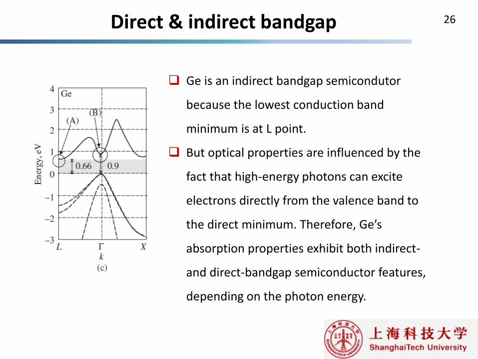
Direct & indirect bandgap 26
Ge is an indirect bandgap semicondutor
because the lowest conduction band
minimum is at L point.
But optical properties are influenced by the
fact that high-energy photons can excite
electrons directly from the valence band to
the direct minimum. Therefore, Ge’s
absorption properties exhibit both indirect-
and direct-bandgap semiconductor features,
depending on the photon energy.
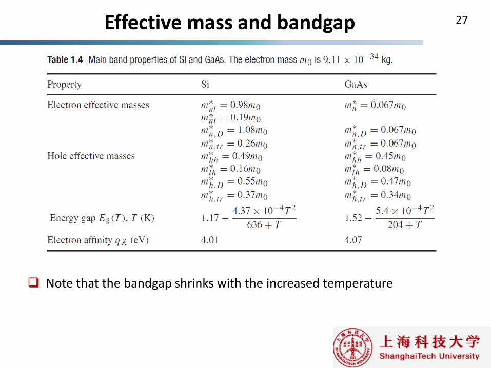
Effective mass and bandgap 27
Note that the bandgap shrinks with the increased temperature
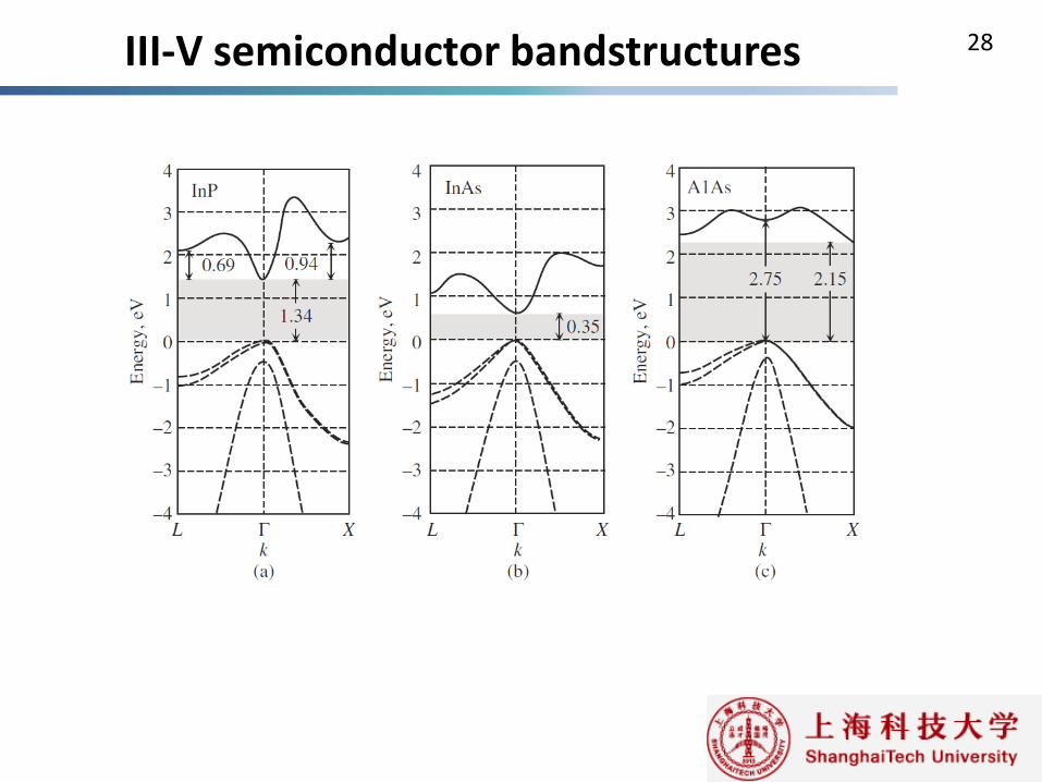
III-V semiconductor bandstructures 28
Lecture 3 29
Carrier densities in semiconductors
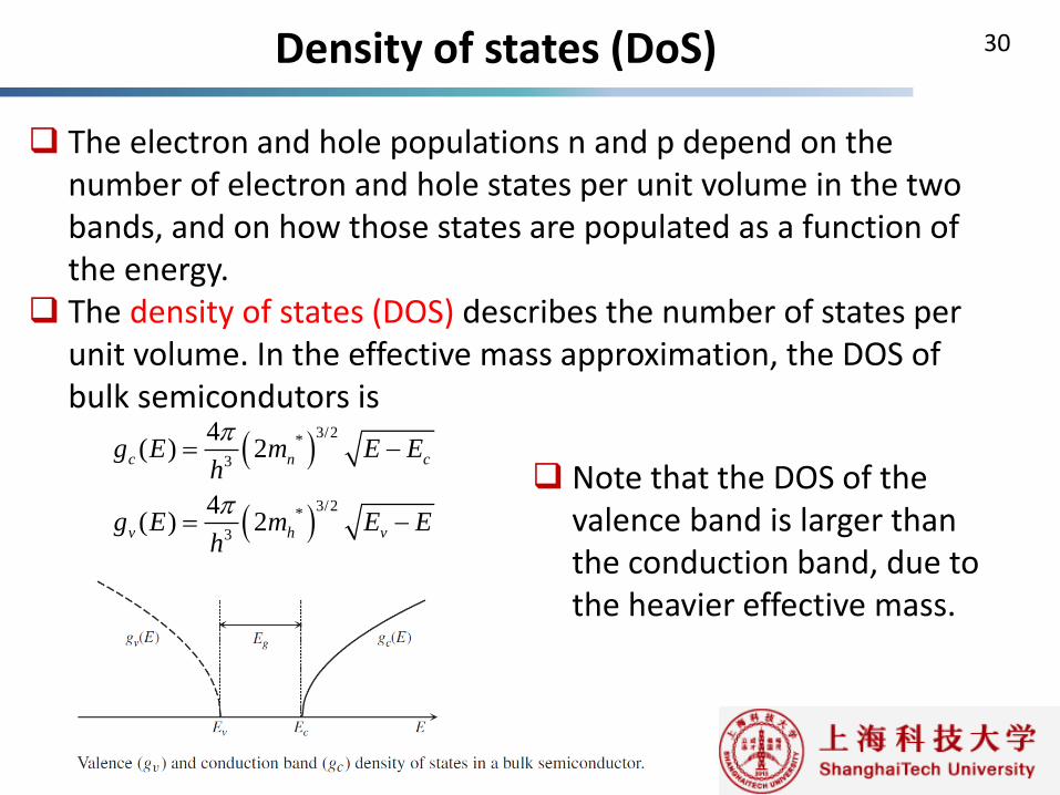
Density of states (DoS) 30
3/2*
3
3/2*
3
4( ) 2
4( ) 2
c n c
v h v
g E m E Eh
g E m E Eh
The electron and hole populations n and p depend on the number of electron and hole states per unit volume in the two bands, and on how those states are populated as a function of the energy.
The density of states (DOS) describes the number of states per unit volume. In the effective mass approximation, the DOS of bulk semicondutors is
Note that the DOS of the valence band is larger than the conduction band, due to the heavier effective mass.
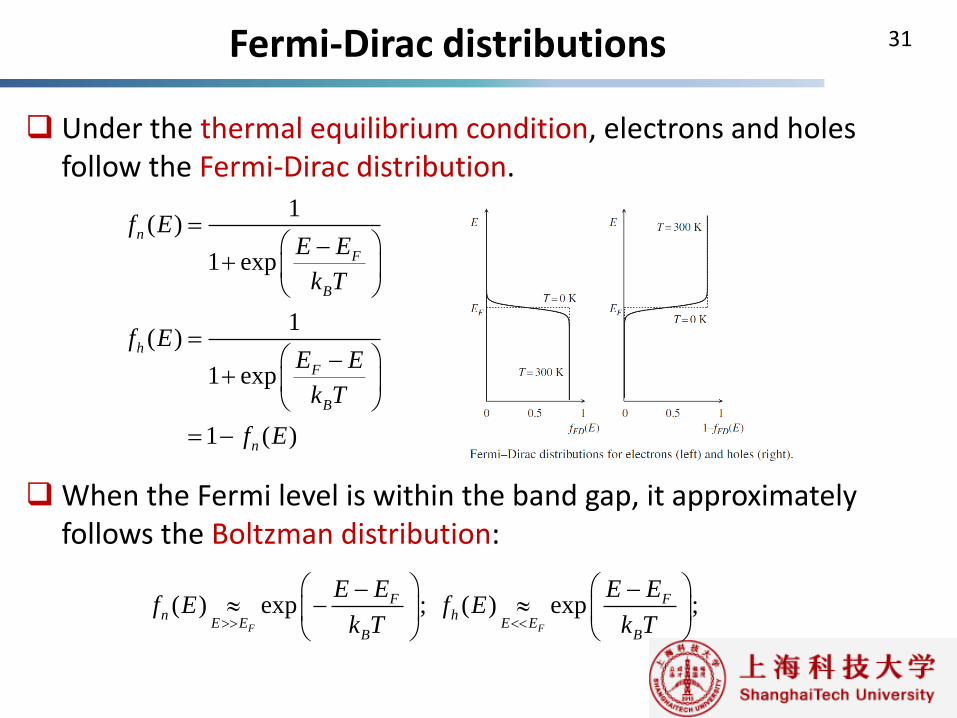
Fermi-Dirac distributions 31
Under the thermal equilibrium condition, electrons and holes follow the Fermi-Dirac distribution.
1( )
1 exp
1( )
1 exp
1 ( )
n
F
B
h
F
B
n
f EE E
k T
f EE E
k T
f E
When the Fermi level is within the band gap, it approximately follows the Boltzman distribution:
( ) exp ; ( ) exp ;F F
F Fn h
E E E EB B
E E E Ef E f E
k T k T
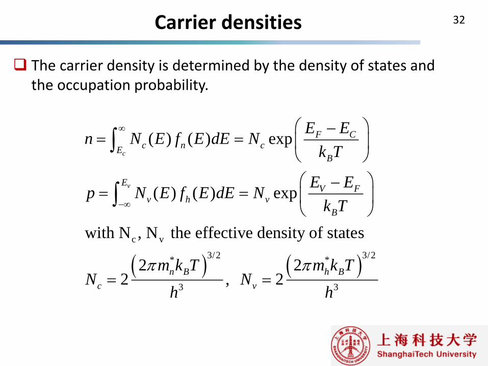
Carrier densities 32
The carrier density is determined by the density of states and the occupation probability.
c v
3/2 3/2* *
3 3
( ) ( ) exp
( ) ( ) exp
with N , N the effective density of states
2 22 , 2
c
v
F Cc n c
EB
EV F
v h v
B
n B h B
c v
E En N E f E dE N
k T
E Ep N E f E dE N
k T
m k T m k TN N
h h
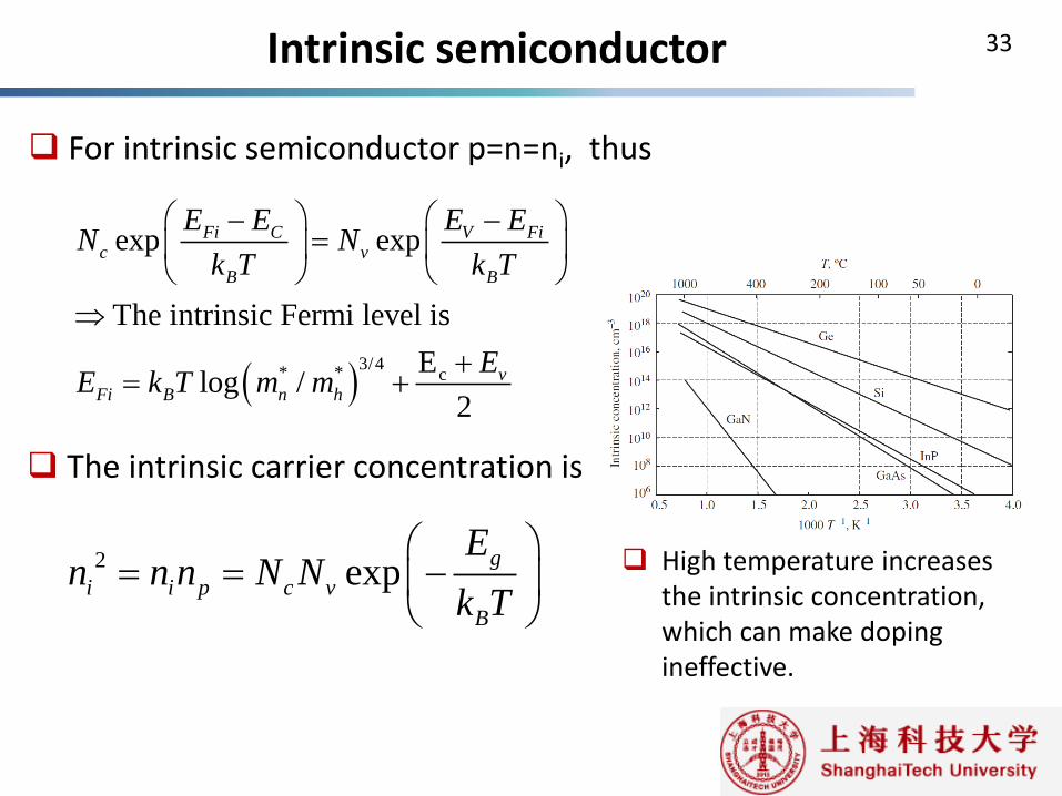
Intrinsic semiconductor 33
For intrinsic semiconductor p=n=ni, thus
3/4
* * c
exp exp
The intrinsic Fermi level is
Elog /
2
Fi C V Fic v
B B
vFi B n h
E E E EN N
k T k T
EE k T m m
The intrinsic carrier concentration is
2 exp
g
i i p c v
B
En n n N N
k T
High temperature increases the intrinsic concentration, which can make doping ineffective.
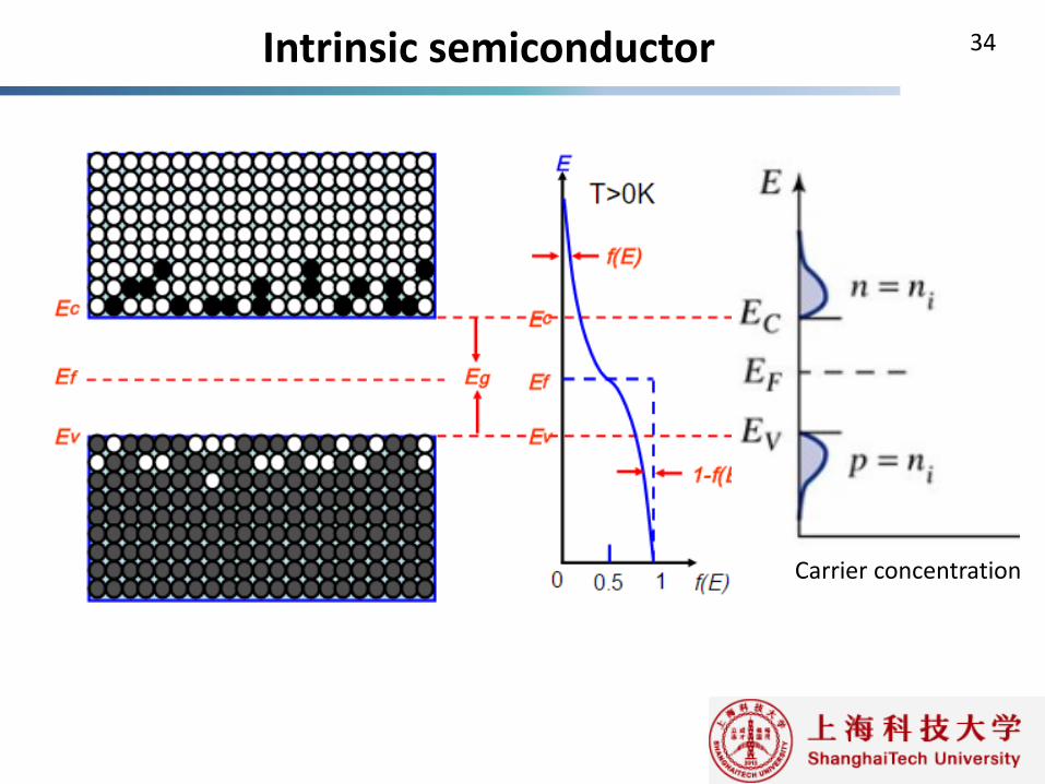
Intrinsic semiconductor 34
Carrier concentration
Mass action law 35
In equilibrium conditions, the product of carrier densities n and
p does not depend on the position of the Fermi level (while the
Fermi level can be changed by the doping). This is coined the
mass action law (质量作用定律), which also holds for doped
semiconductors.
2
inp n
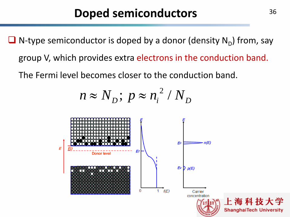
Doped semiconductors 36
N-type semiconductor is doped by a donor (density ND) from, say
group V, which provides extra electrons in the conduction band.
The Fermi level becomes closer to the conduction band.
2; /D i Dn N p n N
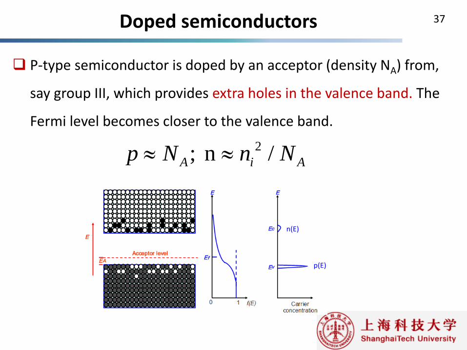
Doped semiconductors 37
P-type semiconductor is doped by an acceptor (density NA) from,
say group III, which provides extra holes in the valence band. The
Fermi level becomes closer to the valence band.
2; n /A i Ap N n N
n(E)
p(E)
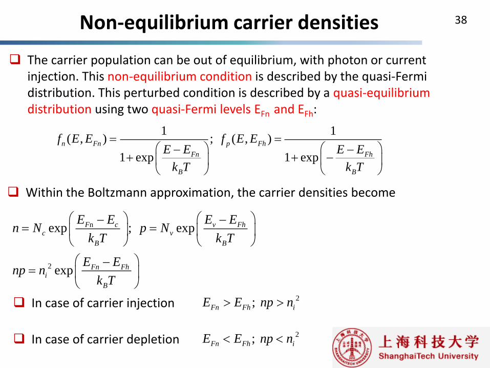
Non-equilibrium carrier densities 38
The carrier population can be out of equilibrium, with photon or current injection. This non-equilibrium condition is described by the quasi-Fermi distribution. This perturbed condition is described by a quasi-equilibrium distribution using two quasi-Fermi levels EFn and EFh:
1 1( , ) ; ( , )
1 exp 1 exp
n Fn p Fh
Fn Fh
B B
f E E f E EE E E E
k T k T
Within the Boltzmann approximation, the carrier densities become
n
2
exp ; exp
exp
F c v Fhc v
B B
Fn Fhi
B
E E E En N p N
k T k T
E Enp n
k T
In case of carrier injection 2; Fn Fh iE E np n
In case of carrier depletion 2; Fn Fh iE E np n
Lecture 4 39
Heterostructures & bandstructure engineering
Heterostructures 40
Crystals with different lattice constants epitaxially grown together is called heterostructure/heterojunction.
The material dicontinuity arising in the heterojunction leads to improvement of electronic and optical properties, such as confinement of carriers owing to band gap difference, and confinement of photons owing to the refractive index difference.
Heterostructures can be lattice-matched (same lattice constant) or affected by a slight mismatch (maximum on the order of 1%), which induces tensile or compressive strain. This is named strained heterostructures.
A double heterostructure made with a thin semiconductor layer (on the order of 100 nm), sandwiched between two layers creates a quantum well.
A succession of weakly interacting Qwells is called multi quantum wells (MQW). If the MQW has many layers, with significant overlapping between the
wavefunctions of adjacent wells, we obtain a superlattice.
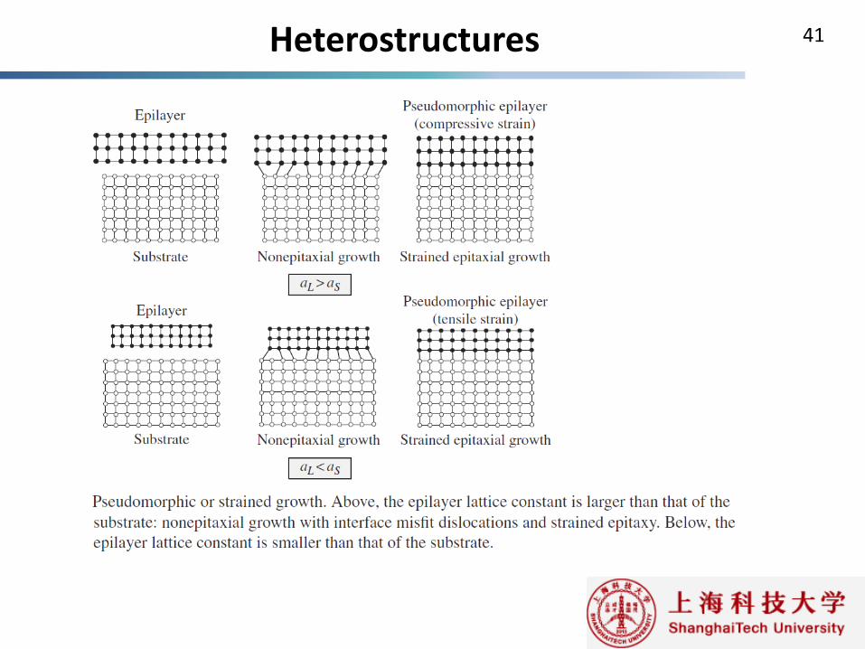
Heterostructures 41
Semiconductor alloys 42
Heterostructures are largely based on semiconductor alloys. One motivation of alloys is for obtaining certain bandgap, by tailoring the lattice constant, which approximately follow a linear law with respect to the individual component parameters. The other motivation is to achieve lattice matching to the substrate.
Alloys can be made of two (binary), three (ternary), or four (quarnery) elements. AlGaAs is alloy of GaAs and AlAs; InGaAsP is alloy of InAs, InP, GaAs and GaP. By proper selection of the alloy composition, semiconductor alloys emitting the right wavelength and matched to the right substrate can be generated.
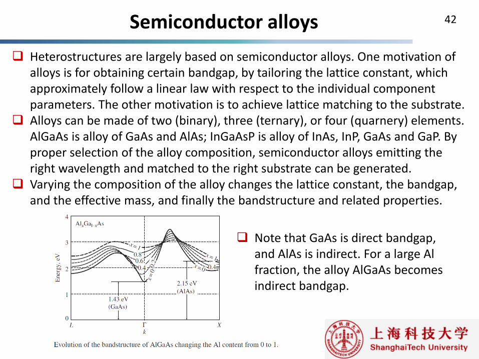
Varying the composition of the alloy changes the lattice constant, the bandgap, and the effective mass, and finally the bandstructure and related properties.
Note that GaAs is direct bandgap, and AlAs is indirect. For a large Al fraction, the alloy AlGaAs becomes indirect bandgap.
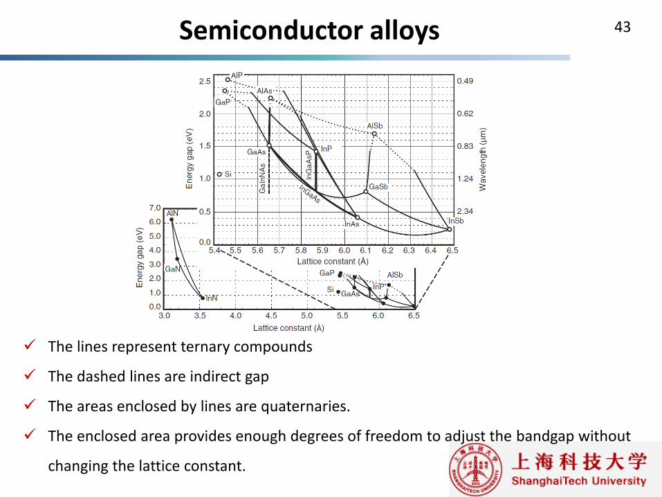
Semiconductor alloys 43
The lines represent ternary compounds
The dashed lines are indirect gap
The areas enclosed by lines are quaternaries.
The enclosed area provides enough degrees of freedom to adjust the bandgap without
changing the lattice constant.
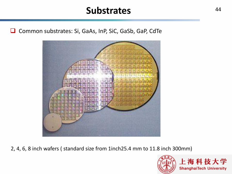
Substrates 44
Common substrates: Si, GaAs, InP, SiC, GaSb, GaP, CdTe
2, 4, 6, 8 inch wafers ( standard size from 1inch25.4 mm to 11.8 inch 300mm)
Bandstructure engineering 45
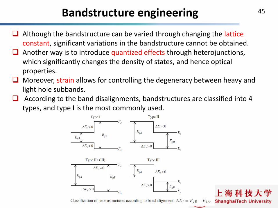
Although the bandstructure can be varied through changing the lattice constant, significant variations in the bandstructure cannot be obtained.
Another way is to introduce quantized effects through heterojunctions, which significantly changes the density of states, and hence optical properties.
Moreover, strain allows for controlling the degeneracy between heavy and light hole subbands.
According to the band disalignments, bandstructures are classified into 4 types, and type I is the most commonly used.
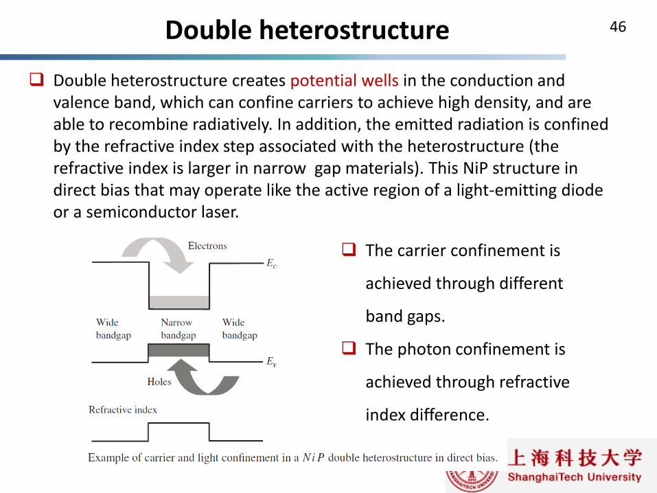
Double heterostructure 46
Double heterostructure creates potential wells in the conduction and valence band, which can confine carriers to achieve high density, and are able to recombine radiatively. In addition, the emitted radiation is confined by the refractive index step associated with the heterostructure (the refractive index is larger in narrow gap materials). This NiP structure in direct bias that may operate like the active region of a light-emitting diode or a semiconductor laser.
The carrier confinement is
achieved through different
band gaps.
The photon confinement is
achieved through refractive
index difference.
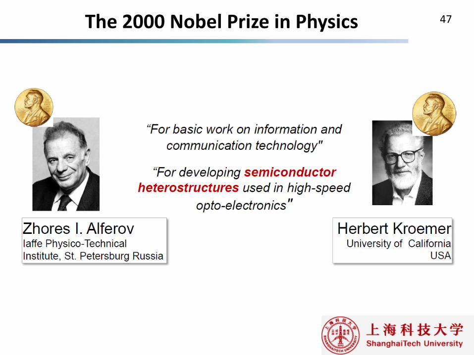
The 2000 Nobel Prize in Physics 47

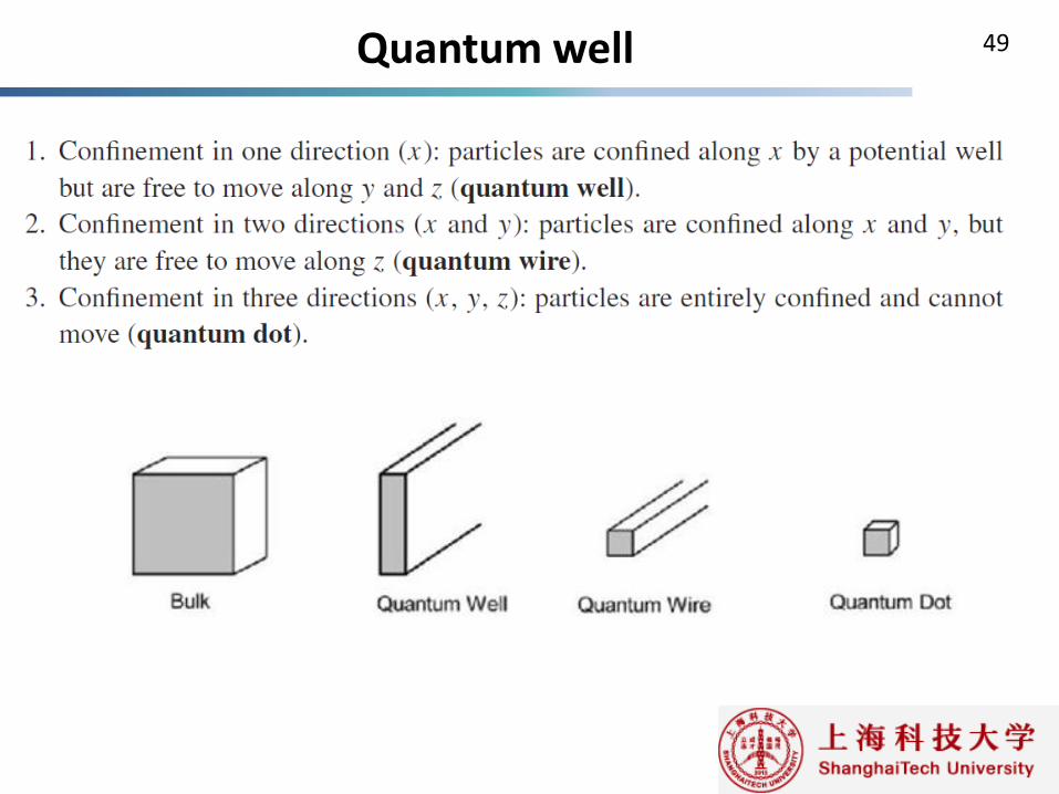
Quantum well 48
In case the potential well is very narrow, the allowed energy levels of the
confined electrons and holes will be quantized, leading to quantum well
structure. It has a different bandstructure vs. bulk, where sets of energy
subbands appear, and density of states is strongly affected.
The QW bandstructure can be calculated by the Schrodinger equation by a 3D
effective mass approximation.
Quantum well 49
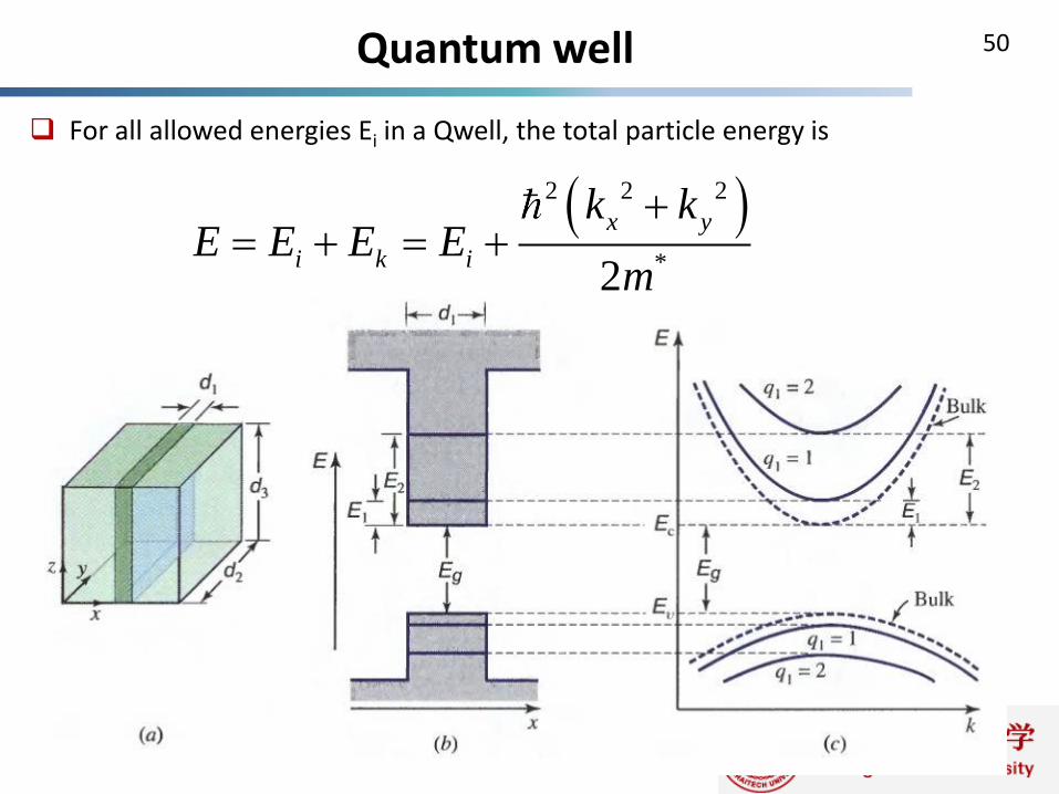
Quantum well 50
For all allowed energies Ei in a Qwell, the total particle energy is
2 2 2
*2
x y
i k i
k kE E E E
m
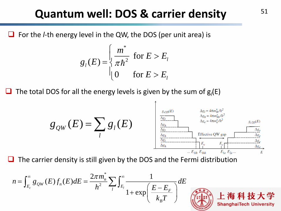
Quantum well: DOS & carrier density 51
For the l-th energy level in the QW, the DOS (per unit area) is
*
2 for
( )
0 for
l
l
l
mE E
g E
E E
The total DOS for all the energy levels is given by the sum of gl(E)
( ) ( )QW l
l
g E g E
The carrier density is still given by the DOS and the Fermi distribution
*
2
2 1( ) ( )
1 expc l
nQW n
E El F
B
mn g E f E dE dE
h E E
k T
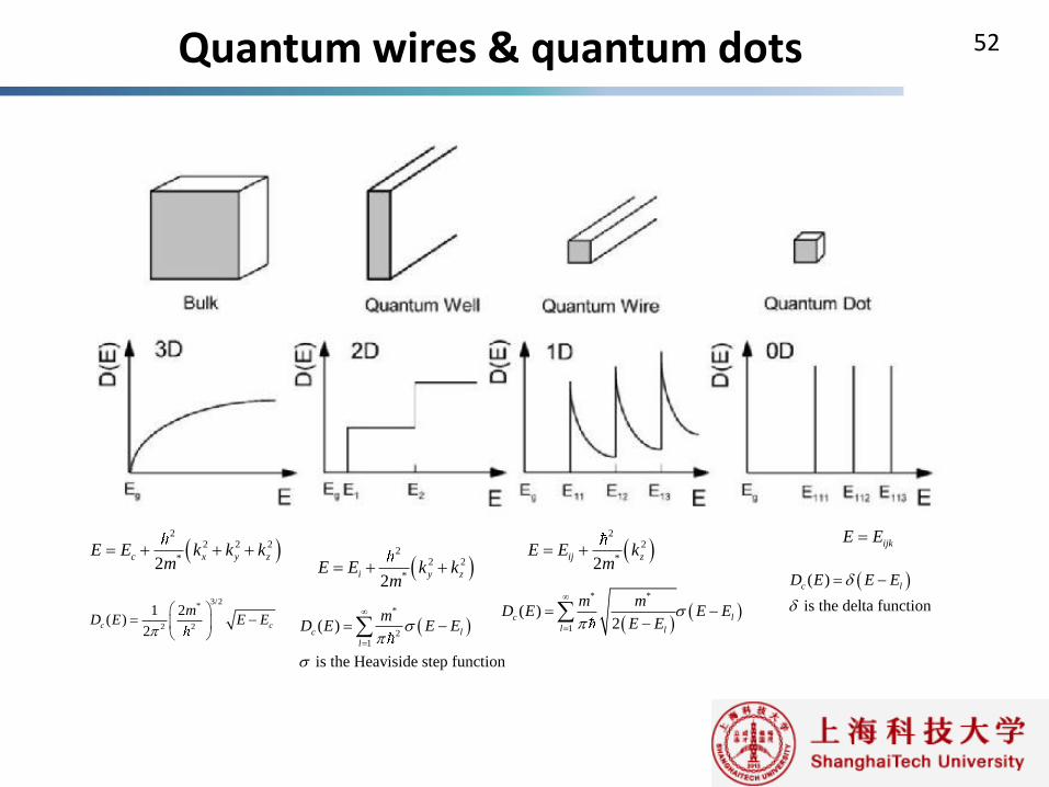
Quantum wires & quantum dots 52
2
2 2 2
*2c x y zE E k k k
m
3/2*
2 2
1 2( )
2c c
mD E E E
2
2 2
*2i y zE E k k
m
*
21
( )
is the Heaviside step function
c l
l
mD E E E
2
2
*2ij zE E k
m
* *
1
( )2
c l
l l
m mD E E E
E E
ijkE E
( )
is the delta function
c lD E E E
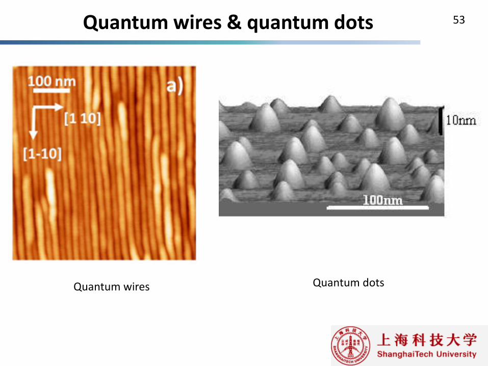
53 Quantum wires & quantum dots
Quantum wires Quantum dots
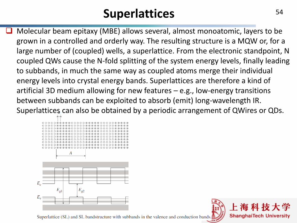
Superlattices 54
Molecular beam epitaxy (MBE) allows several, almost monoatomic, layers to be grown in a controlled and orderly way. The resulting structure is a MQW or, for a large number of (coupled) wells, a superlattice. From the electronic standpoint, N coupled QWs cause the N-fold splitting of the system energy levels, finally leading to subbands, in much the same way as coupled atoms merge their individual energy levels into crystal energy bands. Superlattices are therefore a kind of artificial 3D medium allowing for new features – e.g., low-energy transitions between subbands can be exploited to absorb (emit) long-wavelength IR. Superlattices can also be obtained by a periodic arrangement of QWires or QDs.
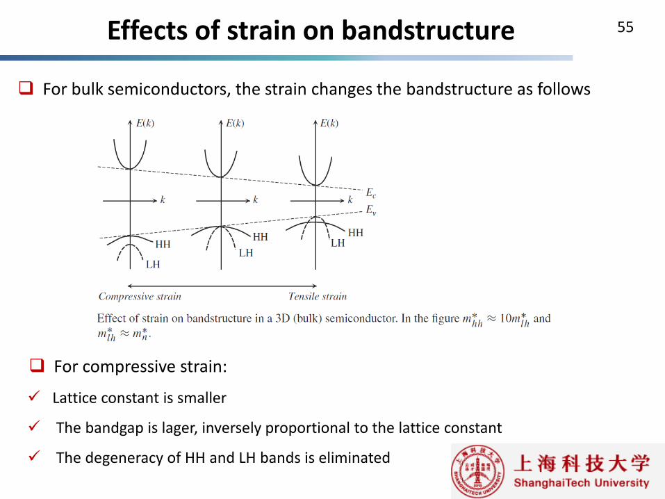
Effects of strain on bandstructure 55
For bulk semiconductors, the strain changes the bandstructure as follows
Lattice constant is smaller
The bandgap is lager, inversely proportional to the lattice constant
The degeneracy of HH and LH bands is eliminated
For compressive strain:
Lecture 5 56
Carrier generation and recombination
Generation & recombination 57
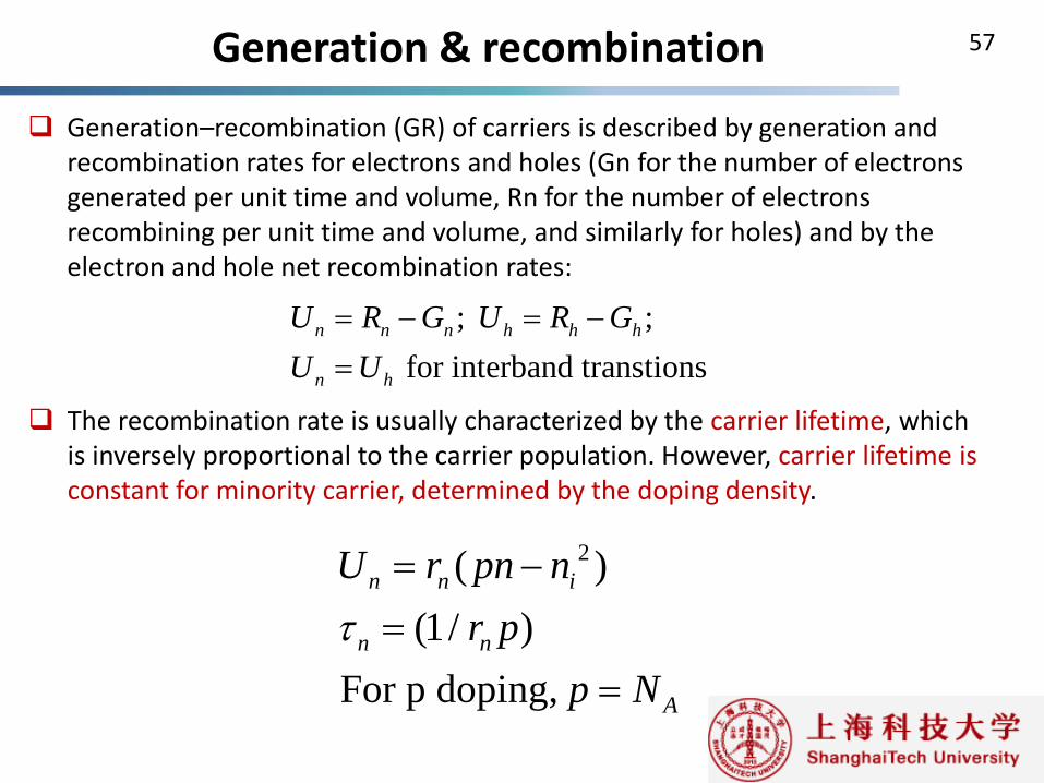
Generation–recombination (GR) of carriers is described by generation and recombination rates for electrons and holes (Gn for the number of electrons generated per unit time and volume, Rn for the number of electrons recombining per unit time and volume, and similarly for holes) and by the electron and hole net recombination rates:
; ;
for interband transtions
n n n h h h
n h
U R G U R G
U U
The recombination rate is usually characterized by the carrier lifetime, which is inversely proportional to the carrier population. However, carrier lifetime is constant for minority carrier, determined by the doping density.
2( )
(1/ )
For p doping,
n n i
n n
A
U r pn n
r p
p N
Generation & recombination 58
GR mechanisms can be phonon-assisted or thermal, photon-assisted or radiative
(optical), and, finally, assisted by other electrons or holes. Moreover, generation
and recombination can occur through interband transitions (direct mechanisms),
or through indirect mechanism assisted by intermediate trap levels in the
forbidden band. In direct-bandgap semiconductors, direct optical GR is typically
the dominant mechanism, whereas in indirect-bandgap semiconductors trap-
assisted GR can be a stronger competitor to the weaker optical GR.
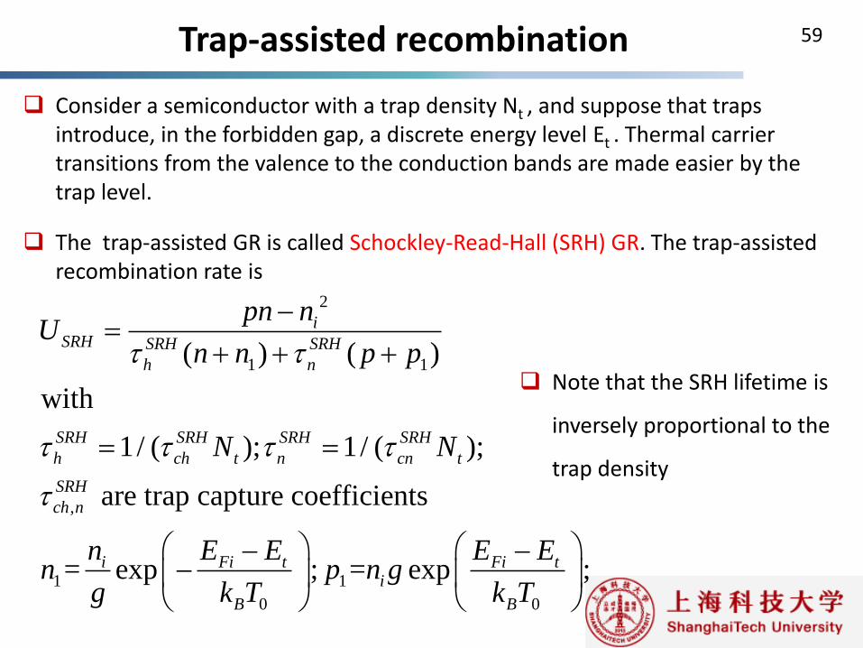
Trap-assisted recombination 59
Consider a semiconductor with a trap density Nt , and suppose that traps introduce, in the forbidden gap, a discrete energy level Et . Thermal carrier transitions from the valence to the conduction bands are made easier by the trap level.
The trap-assisted GR is called Schockley-Read-Hall (SRH) GR. The trap-assisted recombination rate is
2
1 1
,
1 1
0 0
( ) ( )
with
1/ ( ); 1/ ( );
are trap capture coefficients
= exp ; = exp ;
iSRH SRH SRH
h n
SRH SRH SRH SRH
h ch t n cn t
SRH
ch n
i Fi t Fi ti
B B
pn nU
n n p p
N N
n E E E En p n g
g k T k T
Note that the SRH lifetime is
inversely proportional to the
trap density
Trap-assisted recombination 60
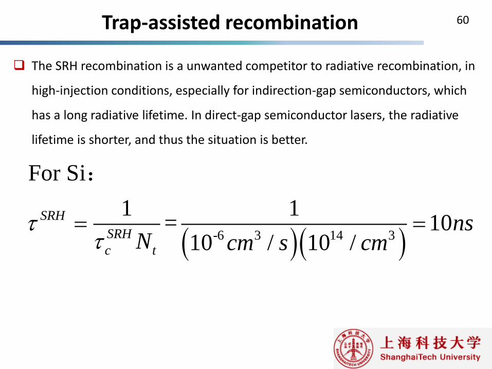
The SRH recombination is a unwanted competitor to radiative recombination, in
high-injection conditions, especially for indirection-gap semiconductors, which
has a long radiative lifetime. In direct-gap semiconductor lasers, the radiative
lifetime is shorter, and thus the situation is better.
-6 3 14 3
For Si
1 1= 10
10 / 10 /
SRH
SRH
c t
nsN cm s cm
:
Auger recombination & generation 61
The electron- or hole-assisted recombination is called Auger recombination, and
the related rate is proportional to p2n or pn2. The Auger recombination is
important (unwanted competitor of radiative recombination) in high-injection
devices like semiconductor lasers.
Impact ionization (碰撞电离) is an inverse process of Auger recombination. In
high-field conditions (i.e., for fields of the order of 100 kV/cm), electrons and
holes gather enough energy from the electric field between two successive
scattering events (i.e., collisions with phonons, impurities) to be able to interact
with another electron and promote it to the conduction band. Each electron or
hole is therefore able to generate, over a certain length, a number of electron–
hole pairs. The resulting chain can lead to diverging current, i.e., to avalanche
breakdown in the semiconductor. This effect is used to get avalanche
photodiode (APD).
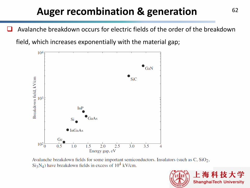
Auger recombination & generation 62
Avalanche breakdown occurs for electric fields of the order of the breakdown
field, which increases exponentially with the material gap;