Semiconductor memories. Memories 2/38 Types of semiconductor memories Memory chip parameters Chosen...
38
Semiconductor memories
Transcript of Semiconductor memories. Memories 2/38 Types of semiconductor memories Memory chip parameters Chosen...

Semiconductor memories

Memories 2/38
Types of semiconductor memories
Memory chip parameters
Chosen types of memories
Memory map
Timings

Memories 3/38
timersRTC
address decoders
memory servicing devices
interruptcontrollers
secondarymemories.
processor
programme memory(ROM)
datamemory(RAM)
operatordevices
commu-nication devices
process devicesmain memory
video memory
The application of semiconductor memories:
semiconductor disksconfigur. memory
buffering memories

Memories - types 4/38
Semiconductor memories
shiftingregisters
CCD - charge coupling
devices
with sequence access
volatile non-volatile
static dynamic (SRAM) (DRAM)
parallel classic (bipol.,unipol.) (unipol.)
serial pseudo-static (unipol.) (unipol.)
standard
memory losingdata duringpower off
memory keepingdata duringpower off

Memories - SRAM 5/38
Single bit of SRAM:
RDamplifier
wordselectline
+U
+U
bipolar
wordselectline
RDamplifier
Udd
Udd
Uss=0
unipolar

Memories - SRAM 6/38
read
ADR
CE
R/W
D0..D7
Typical read and write cycles of SRAM
write
ADR
CE
R/W
D0..D7

Memories - SRAM 7/38
SRAM examples:
symbol manufacturer organization access time[ns]
ICC/ISB 1
[mA]2114A Intel 1kx4 100-250 70/-
HM6116-12 Hitachi 2kx8 120 80/15
HM6264P Hitachi 8kx8 100-150 110/3
HM62256P Hitachi 32kx8 85-150 70/3
FCB61C1025 Philips 128kx8 35-55 80/3
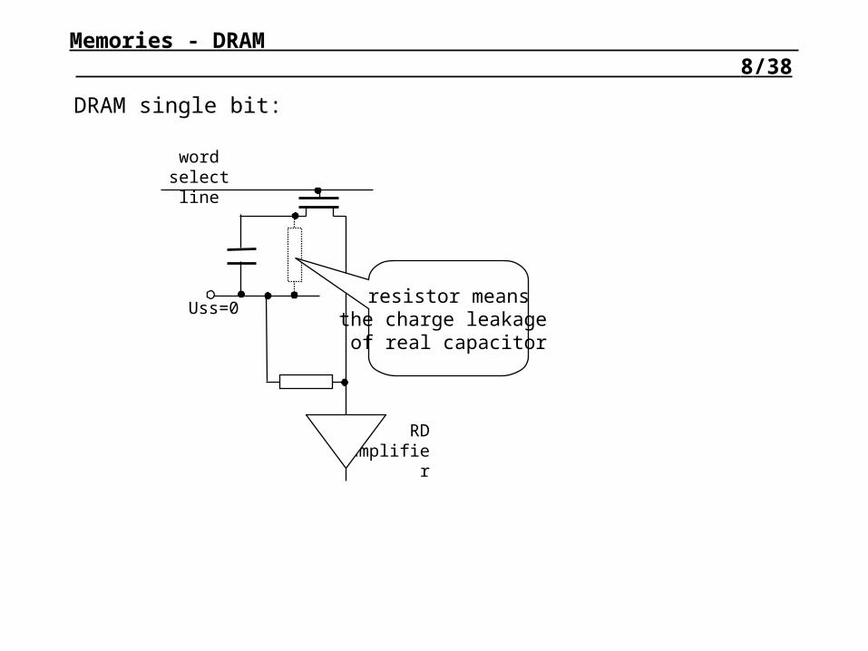
Memories - DRAM 8/38
DRAM single bit:
Uss=0
wordselectline
RDamplifier
resistor meansthe charge leakage
of real capacitor

Memories - DRAM 9/38
Advantages Faults
low power consumption;
high speeds;
large capacities;
small cases.
data refresh needed
(the charge in DRAM cell should be refreshed
each 2-16ms);
multiplexed address lines;
non-standard control.

Memories - DRAM 10/38
Basic cycles:
A8..A15A0..A7writing ADR
RAS
CAS
WE
DATA Din
A8..A15A0..A7reading ADR
RAS
CAS
DATA
tACAS
tARAS
Dout
WE = 1

Memories - DRAM 11/38
modification A8..A15A0..A7ADR
RAS
CAS
WE
Dout
Din Din
Dout
page read
Dout
A8..A15A8..A15A0..A7ADR
RAS
CAS
DATA Dout
WE = 1

Memories - DRAM 12/38
basic refresh cycle
row addressADR
RASWE = 1
CAS = 1
ADR
RAS
CAS
DATA
hidden refresh cycle
A8..A15REFA8..A15A0..A7
Dout
WE = 1

Memories - DRAM 13/38
DRAM refresh techniques:
1. Burst refresh - for instance each 2ms processor is stopped
and the whole set of rows addresses needed for memory refresh is generated.
2. Cycle steal - generation of successive refresh addresses realised
in the moments, in which processor doesn’t used the system bus
(for example after op-code fetch), but there are situations that processor
is halted or held by DMA and refresh should be realised in other way.
Attention:
Modern DRAM chip have built-in refresh circuit.
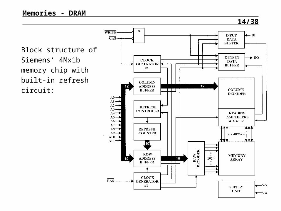
Memories - DRAM 14/38
Block structure of Siemens’
4Mx1b memory chip with
built-in refresh circuit:

Memories - DRAM 15/38
A7..A13
A0..A6MPX DRAM
A0
A6
CAS RAS
ADR0...
ADR6
MREQ
RFSH
50ns
50nsthere are also special
DRAM control chips: 3242, 8202 (IBM PC)
Example of simple DRAM control circuit:
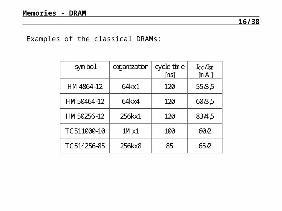
Memories - DRAM 16/38
symbol organization cycle time[ns]
ICC/ISB
[mA]
HM4864-12 64kx1 120 55/3,5
HM50464-12 64kx4 120 60/3,5
HM50256-12 256kx1 120 83/4,5
TC511000-10 1Mx1 100 60/2
TC514256-85 256kx8 85 65/2
Examples of the classical DRAMs:
Memories - DRAM 17/38
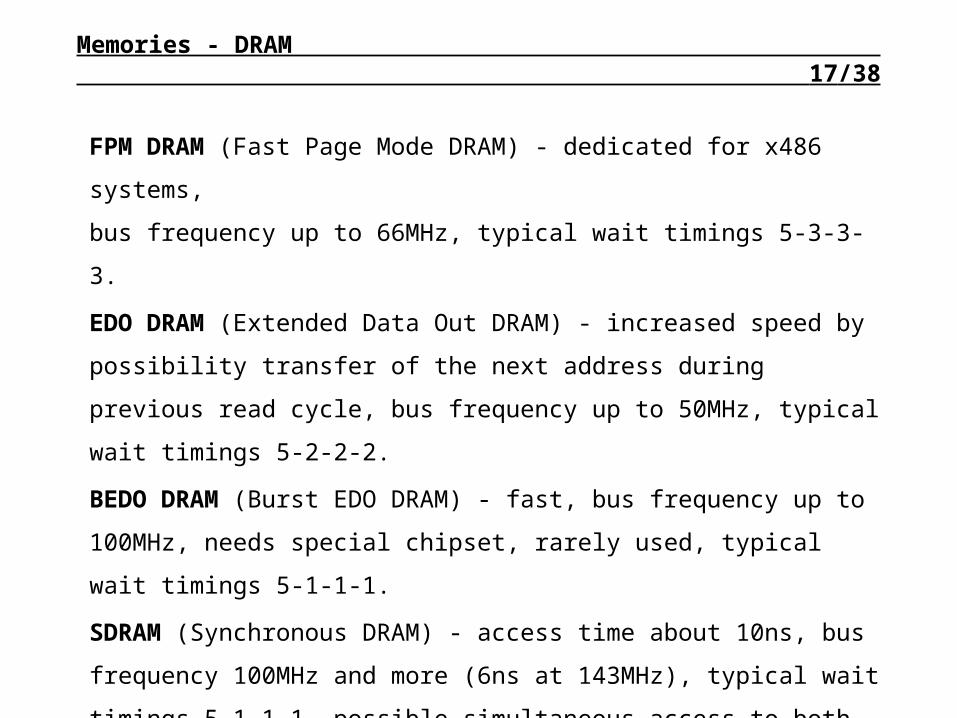
FPM DRAM (Fast Page Mode DRAM) - dedicated for x486 systems,
bus frequency up to 66MHz, typical wait timings 5-3-3-3.
EDO DRAM (Extended Data Out DRAM) - increased speed by possibility
transfer of the next address during previous read cycle, bus frequency up to
50MHz, typical wait timings 5-2-2-2.
BEDO DRAM (Burst EDO DRAM) - fast, bus frequency up to 100MHz, needs
special chipset, rarely used, typical wait timings 5-1-1-1.
SDRAM (Synchronous DRAM) - access time about 10ns, bus frequency 100MHz
and more (6ns at 143MHz), typical wait timings 5-1-1-1, possible simultaneous
access to both open pages, built-in auto-refresh.

Memories - DRAM 18/38
DDR SDRAM (Double Data Rate SDRAM) - transfer on both slopes of the
clocking signal - double read speed of data blocks.
ESDRAM (Enhanced SDRAM) - internal SRAM buffers double memory
efficiency.
DRDRAM (Direct Rambus DRAM) - special fast buses with DRDRAM and
frequency up to 400MHz and transfer on both slopes of the clocking signal,
transfer 1,6-2,4GB/s, non-standard mechanical construction.
SLDRAM (Synchronous Link DRAM) - SDRAM extension, transfer speed up to
3,2GB/s, electrically and mechanically compatible with SDRAM.
SGRAM (Synchronous Graphic RAM) - fast (100MHz), single-port memory for
graphic applications.
VRAM (Video RAM) - fast, dual-port memory for graphic applications.

Memories - technologies 19/38
Technology features of memories:
Bipolar:
faster;
bigger power consumption;
lower integration scale;
„more expensive” 1 bit.
Unipolar:
slower;
smaller power consumption;
higher integration scale;
„more cheap” 1 bit.

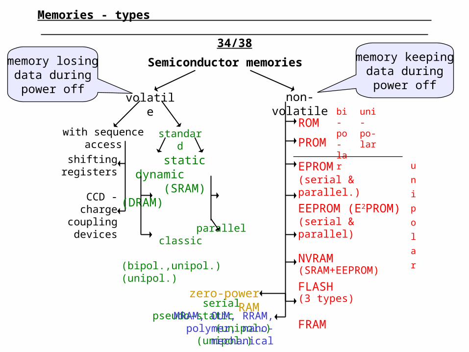
Memories - types 20/38
Semiconductor memories
shiftingregisters
CCD - charge coupling
devices
with sequence access
volatile non-volatile
static dynamic (SRAM) (DRAM)
parallel classic (bipol.,unipol.) (unipol.)
serial pseudo-static (unipol.) (unipol.)
standardROM
PROM
EPROM (serial & parallel.)
EEPROM (E2PROM) (serial & parallel)
NVRAM (SRAM+EEPROM)
FLASH(3 types)
FRAM
bi- po-lar
uni-po-lar
u
n
i
p
o
l
a
r
memory losingdata duringpower off
memory keepingdata duringpower off

Memories - ROM 21/38
Features:
• programmed only during manufacturing;
• long-lasting and expensive manufacturing cycle;
• programme error causes useless of whole chip series;
• expensive debugging (multiple re-designing of chip contents);
• low cost of single memory chip with debugged programme in mass manufacturing.

Memories - PROM 22/38
Single bit PROM:
word select line
Vcc
7V
Q0
Vcc
bit programming:Vcc=12,5V Up=8V
12,5V
12,5V
„0” - 0V
„1” - 8V
Ube

Memories - EPROM 23/38
Single bit EPROM:
DATA BUFFER
RD/WR AMPLIFIER
COLUMN DECODER
ROW
DECODER
ADDRESS
BUFFER
WE/CS
PROG
Memories - EPROM 24/38
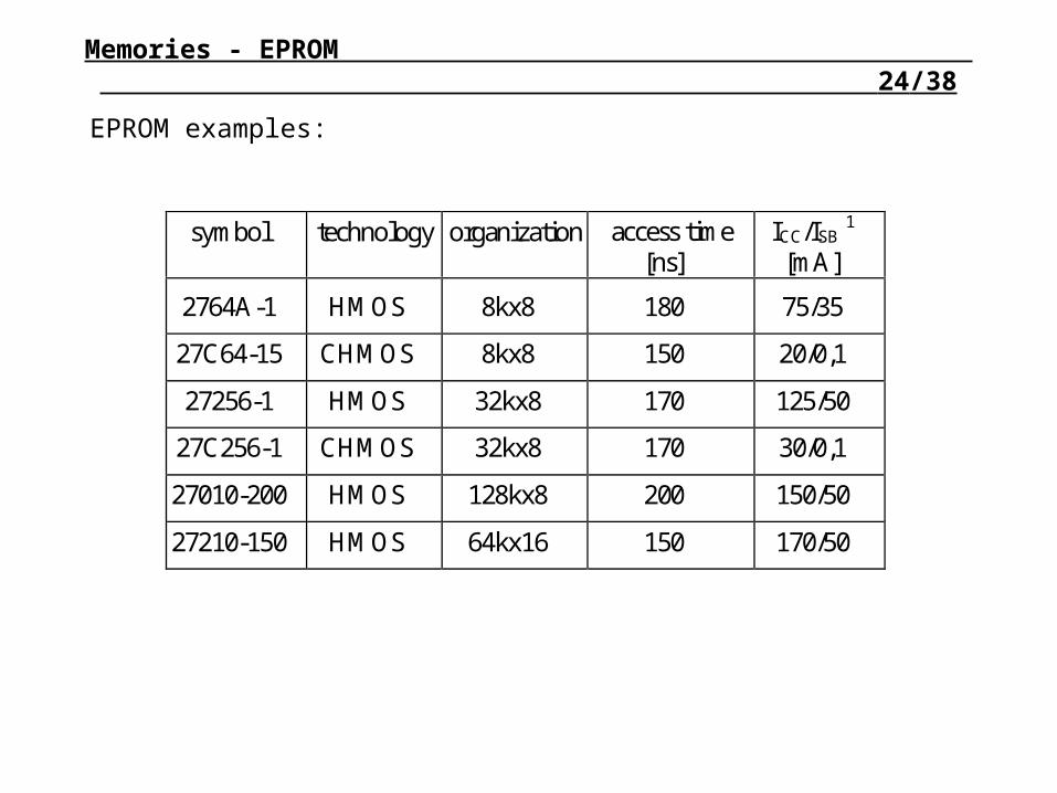
EPROM examples:
symbol technology organization access time[ns]
ICC/ISB 1
[mA]
2764A-1 HMOS 8kx8 180 75/35
27C64-15 CHMOS 8kx8 150 20/0,1
27256-1 HMOS 32kx8 170 125/50
27C256-1 CHMOS 32kx8 170 30/0,1
27010-200 HMOS 128kx8 200 150/50
27210-150 HMOS 64kx16 150 170/50

Memories – EEPROM (E2PROM) 25/38
EEPROM (Electrically Erasable Programmable Read Only Memory) features :
• internal structure based on EPROM;
• additional transistor per each bit allows individual erasing and programming;
• higher number of reprogramming cycles;
• erasing and reprogramming can last up to 10ms;
• with parallel access – equivalent to EPROMs, or serial access (with I2C, SPI)- as a configuration memory;
• parallel EEPROMs can allow programming of blocks of bytes (64B, 128B, 256B): new data is buffered in local SRAM and then simultaneous programming of whole block starts.

Memories - NVRAM 26/38
Example of NVRAM structure:

Memories - NVRAM 27/38
the working of NVRAM:
operating of the built-in capacitor

Memories - FLASH 28/38
structure of storing transistor:
Memories - FLASH 29/38
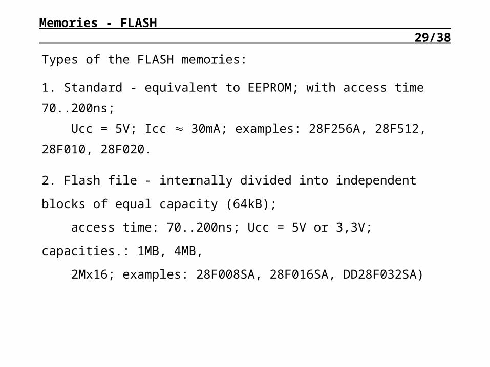
Types of the FLASH memories:
1. Standard - equivalent to EEPROM; with access time 70..200ns;
Ucc = 5V; Icc 30mA; examples: 28F256A, 28F512, 28F010, 28F020.
2. Flash file - internally divided into independent blocks of equal capacity (64kB);
access time: 70..200ns; Ucc = 5V or 3,3V; capacities.: 1MB, 4MB,
2Mx16; examples: 28F008SA, 28F016SA, DD28F032SA)

Memories - FLASH 30/38
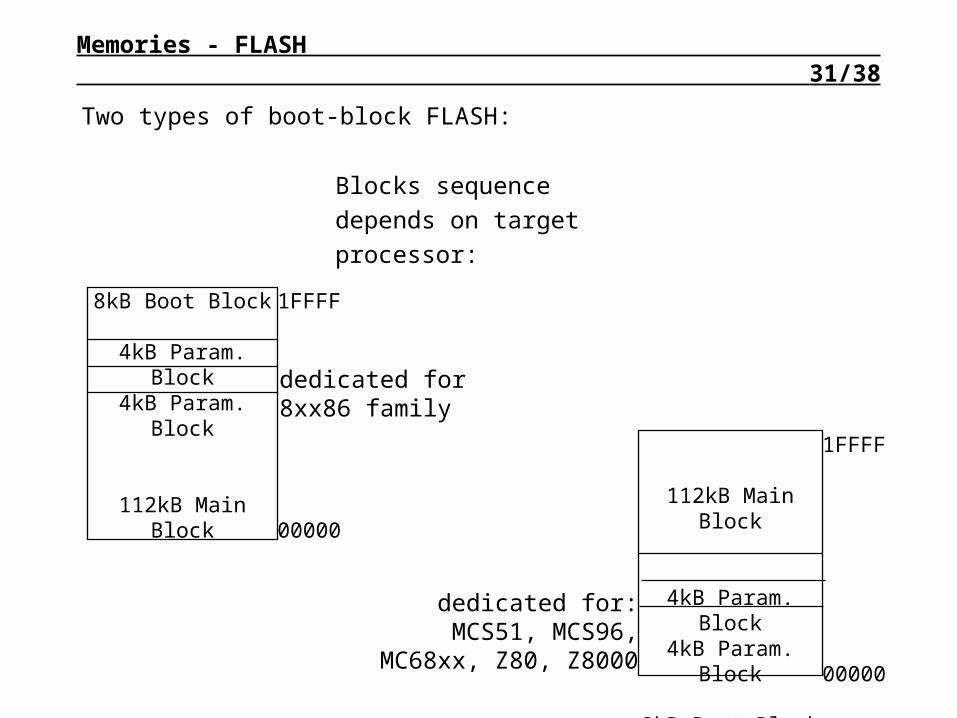
Types of the FLASH memories (cont.):
3. Boot-block flash - characteristic pin RP - Reset-Powerdown,
switching-off memory chip (ISB 0,05A); whole memory divided into
4 specific blocks:
• 8kB Boot Block for initial programme, down-loader;
• 2 x 4kB independent Parameter Block working as configuration memory
instead additional NVRAM or EEPROM chips;
• 112kB Main Block - for the rest of software.
access time 60-150ns; organization 8- or 16-bit; Ucc = 5V or 3,5V;
Memories - FLASH 31/38
Two types of boot-block FLASH:
Blocks sequence depends
on target processor:
8kB Boot Block
4kB Param. Block4kB Param. Block
112kB Main Block
1FFFF
00000
dedicated for 8xx86 family
112kB Main Block
4kB Param. Block4kB Param. Block
8kB Boot Block
1FFFF
00000
dedicated for: MCS51, MCS96, MC68xx,
Z80, Z8000

Memories - FRAM 32/38
Single bit FRAM:
wordselectline
RDamplifier
+U
Uss=0
primary construction
wordselectline
RDamplifier
+U
Uss=0
modified construction
capacitor withferro-electric

Memories - FRAM 33/38
Available FRAMs:
• with serial interfaces: I2C (0,4..1MHz), SPI (2,1..5MHz);
• with parallel interface (for building main-memory blocks);
Memories - types 34/38
Semiconductor memories
shiftingregisters
CCD - charge coupling
devices
with sequence access
volatile non-volatile
static dynamic (SRAM) (DRAM)
parallel classic (bipol.,unipol.) (unipol.)
serial pseudo-static (unipol.) (unipol.)
standardROM
PROM
EPROM (serial & parallel.)
EEPROM (E2PROM) (serial & parallel)
NVRAM (SRAM+EEPROM)
FLASH(3 types)
FRAM
bi- po-lar
uni-po-lar
u
n
i
p
o
l
a
r
memory losingdata duringpower off
memory keepingdata duringpower off
zero-power RAM
MRAM, OUM, RRAM, polymer, nano-mechanical

Memories - zero-power RAM 35/38
Memory structure:

Memories - zero-power RAM 36/38
MRAM - magnetoresistive RAM, two magnetic layers separated by dielectric
OUM (Ovonic Unified Memory) - materials as in CD-RW disks, but writing and
reading realized electrically
RRAM - resistive memory, uses the material which alters its resistance under
electric field
polymer - utilization of the ion structure changes inside polymer under electric
field, high density of bit (also in 3D), transistors need only to control the memory
array
nano-mechanical - np. millipede IBMa

Memories - specific parameters 37/38
Specific parameters of semiconductor memory:
organization (1-bit, k-bit, byte);
capacity (number of data bits stored in chip);
supply parameters (operating voltage / data retention voltage,
operating current / standby current / data retention current);
volatile or non-volatile;
data outputs load capacity;
time characteristic (access time, cycle time, transfer speed).

Memories - specific parameters 38/38
Comparison of chosen memory types
type size data writing reading powerof 1 bit non-volatile time
[ns]number time
[ns]number consumption
SRAM large - 25-100 unlimit. 25-100 unlimit. low
DRAM middle - 50-100 unlimit. 30-70 unlimit. high
EEPROM middle + 10ms 105 60-150 unlimit. middle
NVRAM large + 25-45 unlimit. 25-45 unlimit. middle
Flash small + 5-10s 106 70-150 unlimit. middle
FRAM middle + 150-200 1010-1012 150-200 1010-1012 low