Semiconductor Device Physics Lecture 3 Dr. Gaurav Trivedi, EEE Department, IIT Guwahati.
Upload
charla-blankenshipCategory
view
244download
6
Semiconductor Device Physics
Lecture 4Dr. Gaurav Trivedi,EEE Department,
IIT Guwahati

Electron kinetic energyIn
crea
sing
ele
ctro
n en
ergy
Ec
EvHole kinetic energy In
crea
sing
hol
e en
ergy
c referenceP.E. E E Ec represents the electron potential energy:
Potential vs. Kinetic Energy

c reference
1( )V E Eq
qVP.E.
VdV
dx
E
c v i1 1 1dE dE dE
q dx q dx q dx E
Band Bending The potential energy of a particle with charge –q is related to the electrostatic potential
V(x):
• Since Ec, Ev, and Ei differ only by an additive constant

Ec
Ev
E
x
Until now, Ec and Ev have always been drawn to be independent of the position. When an electric field E exists inside a material, the band energies become a function of
position.
• Variation of Ec with position is called “band bending”
Band Bending

Diffusion Particles diffuse from regions of higher concentration to regions of lower concentration
region, due to random thermal motion (Brownian Motion).

1-D Diffusion Example
Thermal motion causes particles to move into an adjacent compartment every τ seconds.

N|diff N
dnqD
dxJ P|diff P
dpqD
dxJ
Diffusion Currents
• D is the diffusion coefficient [cm2/sec]
n
x
Current flowElectron flow
p
xHole flow

N N|drift N|diff n N dn
q n qDdx
E J J J
P P|drift P|diff p P dp
q p qDdx
EJ J J
Total Currents
Drift current flows when an electric field is applied. Diffusion current flows when a gradient of carrier concentration exist.
N P J J J

N n N 0dn
q n qDdx
EJ
Current Flow Under Equilibrium Conditions In equilibrium, there is no net flow of electrons or :
N 0,J P 0J
The drift and diffusion current components must balance each other exactly. A built-in electric field of ionized atoms exists, such that the drift current exactly cancels out
the diffusion current due to the concentration gradient.
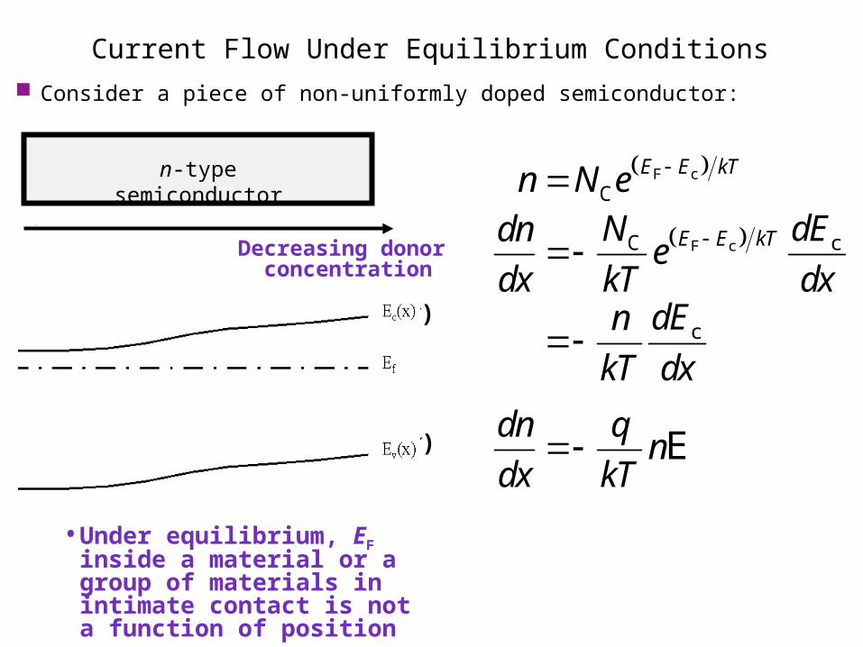
F cC cE E kTN dEdne
dx kT dx
F c
CE E kTn N e
Ev(x)
Ec(x)
EF
dn qn
dx kT E
Current Flow Under Equilibrium Conditions Consider a piece of non-uniformly doped semiconductor:
n-type semiconductor
Decreasing donor concentration
• Under equilibrium, EF inside a material or a group of materials in intimate contact is not a function of position
cdEn
kT dx
N
n
D kT
q
Similarly, P
p
D kT
q
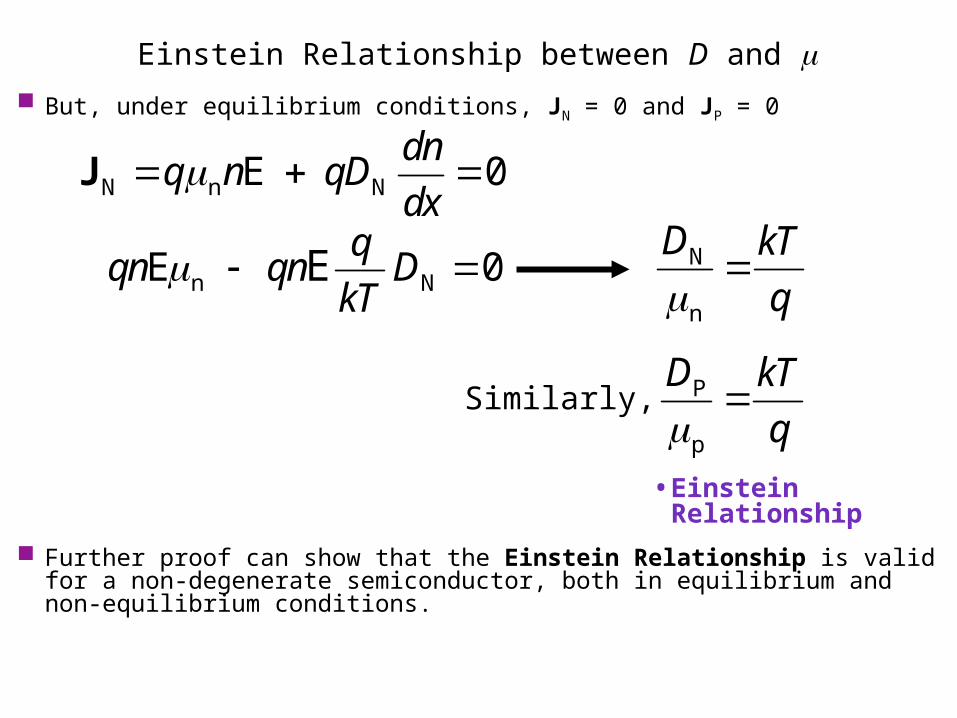
N n N 0dn
q n qDdx
EJ
n N 0q
qn qn DkT
E E
Einstein Relationship between D and m But, under equilibrium conditions, JN = 0 and JP = 0
• Einstein Relationship
Further proof can show that the Einstein Relationship is valid for a non-degenerate semiconductor, both in equilibrium and non-equilibrium conditions.

P p
kTD
q
1 eV1 V
1 e
191 eV 1.602 10 J
Example: Diffusion Coefficient What is the hole diffusion coefficient in a sample of silicon at 300 K with p = 410 cm2 / V.s ?
2 1 125.86 meV410 cm V s
1e
2cm25.86 mV 410
V s
210.603 cm /s
• Remark: kT/q = 25.86 mV at room temperature

Recombination–Generation Recombination: a process by which conduction electrons and holes are annihilated in pairs. Generation: a process by which conduction electrons and holes are created in pairs.
Generation and recombination processes act to change the carrier concentrations, and thereby indirectly affect current flow.
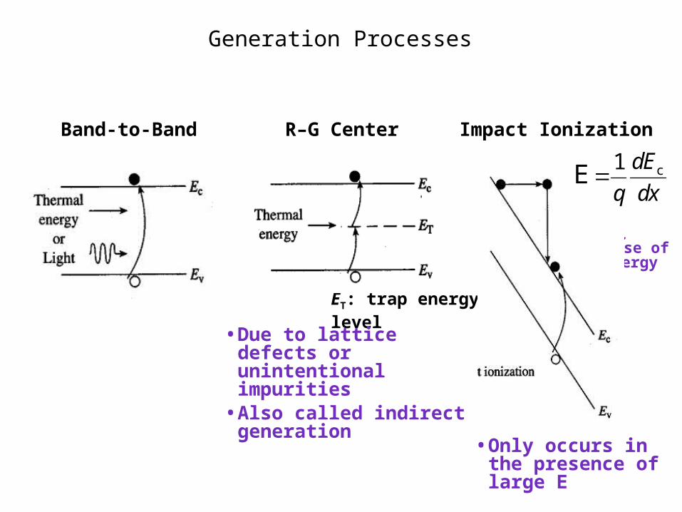
Band-to-Band R–G Center Impact Ionization
EG
c1 dE
q dxE
ET: trap energy level
Generation Processes
Release of energy
• Due to lattice defects or unintentional impurities
• Also called indirect generation
• Only occurs in the presence of large E

Band-to-Band R–G Center Auger
Collision
Recombination Processes
• Rate is limited by minority carrier trapping
• Primary recombination way for Si
• Occurs in heavily doped material

Ev
Ec
Ec
EvGaAs, GaN(direct semiconductors)
Si, Ge(indirect
semiconductors)
PhotonPhoton
Phonon
Direct and Indirect Semiconductors
• Little change in momentum is required for recombination
• Momentum is conserved by photon (light) emission
• Large change in momentum is required for recombination
• Momentum is conserved by mainly phonon (vibration) emission + photon emission
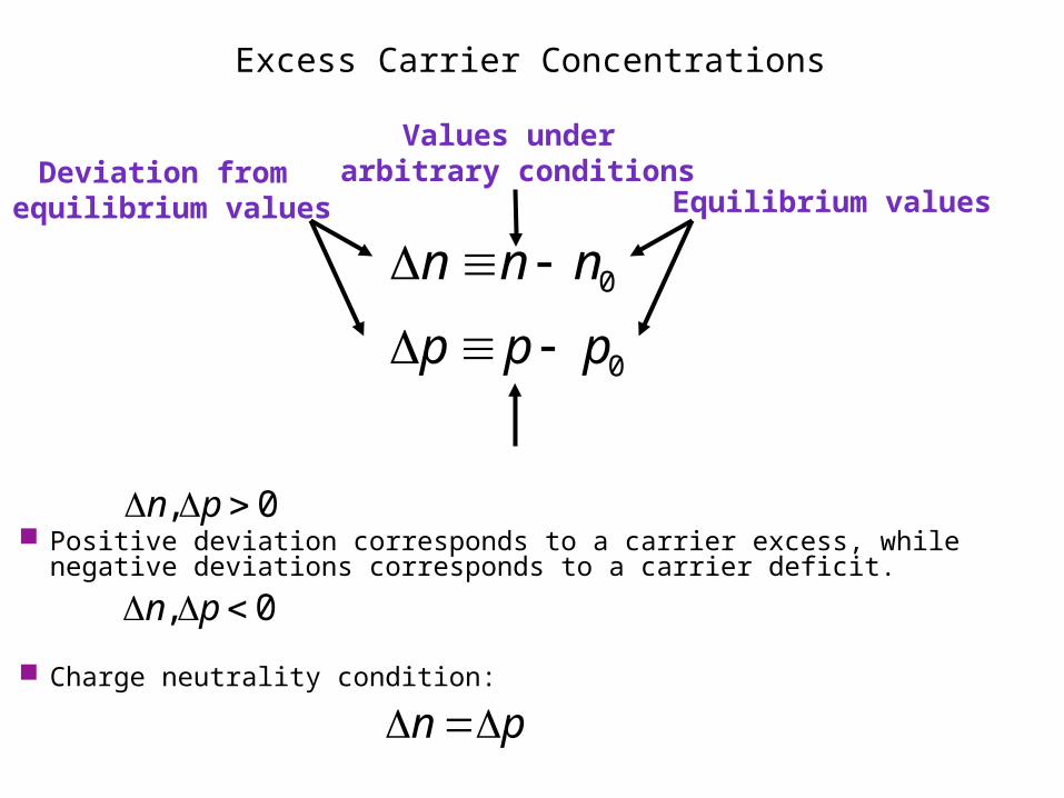
0nnn
0ppp
, 0n p
Equilibrium valuesDeviation from
equilibrium values
Excess Carrier Concentrations
Positive deviation corresponds to a carrier excess, while negative deviations corresponds to a carrier deficit.
Values under arbitrary conditions
pn Charge neutrality condition:
, 0n p

Often, the disturbance from equilibrium is small, such that the majority carrier concentration is not affected significantly:
For an n-type material
For a p-type material
0 0, n p p p
“Low-Level Injection”
However, the minority carrier concentration can be significantly affected.
0p p
0n n • Low-level injection condition

p TR
pc N p
t
G G-equilibrium
p p
t t
NT : number of R–G centers/cm3
Cp : hole capture coefficient
Indirect Recombination Rate Suppose excess carriers are introduced into an n-type Si sample by shining light onto it. At
time t = 0, the light is turned off. How does p vary with time t > 0? Consider the rate of hole recombination:
In the midst of relaxing back to the equilibrium condition, the hole generation rate is small and is taken to be approximately equal to its equilibrium value:
R-equilibrium
p
t
p T 0c N p
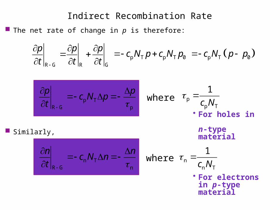
R G R G
p p p
t t t
p TR G p
p pc N p
t
n TR G n
n nc N n
t
pp T
1
c N where
where nn T
1
c N
Indirect Recombination Rate The net rate of change in p is therefore:
p T p T 0c N p c N p p T 0c N p p
• For holes in n-type material
• For electrons in p-type material
Similarly,

pp T n T
1 1 nc N c N
Minority Carrier Lifetime
The minority carrier lifetime τ is the average time for excess minority carriers to “survive” in a sea of majority carriers.
The value of τ ranges from 1 ns to 1 ms in Si and depends on the density of metallic impurities and the density of crystalline defects.
The deep traps originated from impurity and defects capture electrons or holes to facilitate recombination and are called recombination-generation centers.

Example: Photoconductor Consider a sample of Si at 300 K doped with 1016 cm–3 Boron, with recombination lifetime 1
μs. It is exposed continuously to light, such that electron-hole pairs are generated throughout the sample at the rate of 1020 per cm3 per second, i.e. the generation rate GL = 1020/cm3/s.
c) What are p and n?
d) What are np product?
• Note: The np product can be very different from ni
2 in case of perturbed/agitated semiconductor
0p p p 16 1410 10 16 310 cm
0n n n 4 1410 10 14 310 cm
16 1410 10np 30 310 cm 2in
2i
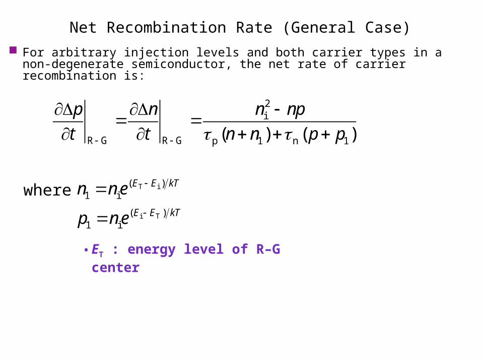
R G R G p 1 n 1( ) ( )
n npp n
t t n n p p
• ET : energy level of R–G center
Net Recombination Rate (General Case) For arbitrary injection levels and both carrier types in a non-degenerate semiconductor, the
net rate of carrier recombination is:
T i( )1 i E E kTn n e
i T( )1 i
E E kTp n e
where