Semiconductor Device Physics Lecture 3 Dr. Gaurav Trivedi, EEE Department, IIT Guwahati.
29
Semiconductor Device Physics Lecture 3 Dr. Gaurav Trivedi, EEE Department, IIT Guwahati
Transcript of Semiconductor Device Physics Lecture 3 Dr. Gaurav Trivedi, EEE Department, IIT Guwahati.

Semiconductor Device Physics
Lecture 3Dr. Gaurav Trivedi,EEE Department,
IIT Guwahati
F( ) /
1( )
1 E E kTf E
e
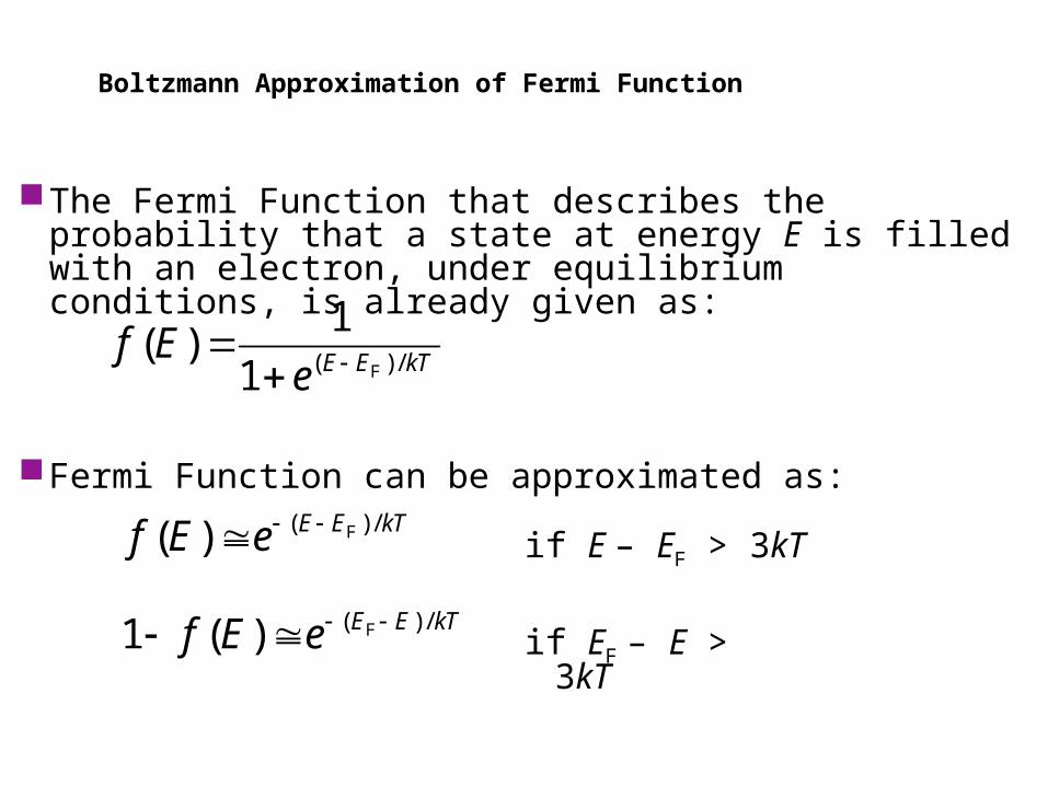
Boltzmann Approximation of Fermi FunctionThe Fermi Function that describes the probability that a state
at energy E is filled with an electron, under equilibrium conditions, is already given as:
Fermi Function can be approximated as:
F( ) /( ) E E kTf E e
F( ) /1 ( ) E E kTf E e
if E – EF > 3kT
if EF – E > 3kT
Boltzmann Approximation of Fermi Function
Boltzmann Approximation of Fermi Function
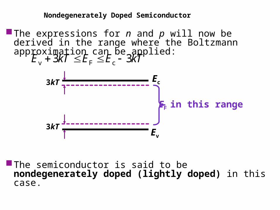
v F c3 3E kT E E kT
The expressions for n and p will now be derived in the range where the Boltzmann approximation can be applied:
The semiconductor is said to be nondegenerately doped (lightly doped) in this case.
Ec
Ev
3kT
3kT
EF in this range
Nondegenerately Doped Semiconductor

Degenerately Doped Semiconductor If a semiconductor is very heavily doped, the Boltzmann
approximation is not valid.For Si at T = 300 K,
Ec-EF < 3kT if ND > 1.6 1018 cm–3
EF-Ev < 3kT if NA > 9.1 1017 cm–3
The semiconductor is said to be degenerately doped (heavily doped) in this case.
• ND = total number of donor atoms/cm3
• NA = total number of acceptor atoms/cm3
Degenerately Doped SemiconductorDegenerately Doped Semiconductor

Boltzmann Approximation of Fermi Function Integrating n(E) over all the energies in the conduction band to obtain n (conduction electron concentration):
top
c
c ( ) ( )E
E
n g E f E dE
By using the Boltzmann approximation, and extending the integration limit to ,
F c
3/ 2*( ) n
C C 2 where 2
2E E kT m kT
n N e Nh
• NC = “effective” density of conduction band states• For Si at 300 K, NC = 3.22 1019 cm–3
Equilibrium Carrier Concentrations

Boltzmann Approximation of Fermi Function Integrating p(E) over all the energies in the conduction band to obtain p (hole concentration):
V
bottom
v ( ) 1 ( )E
E
p g E f E dE
By using the Boltzmann approximation, and extending the integration limit to ,
v F
3/ 2*p( )
V V 2 where 2
2E E kT m kT
p N e Nh
• NV = “effective” density of valence band states• For Si at 300 K, NV = 1.83 1019 cm–3
Equilibrium Carrier Concentrations

Boltzmann Approximation of Fermi FunctionRelationship between EF and n, p :
For intrinsic semiconductors, where n = p = ni,
v F( )V
E E kTp N e
F c( )C
E E kTn N e
G
2i
2 i C V E kT
np n
n N N e
• EG : band gap energy
Intrinsic Carrier Concentration

Boltzmann Approximation of Fermi Functionv c( )
C VE E kTN N e
F c v F( ) ( )C V( ) ( ) E E kT E E kTnp N e N e
GC V
E kTN N e
2i C V
GE kTn N N e
Intrinsic Carrier Concentration
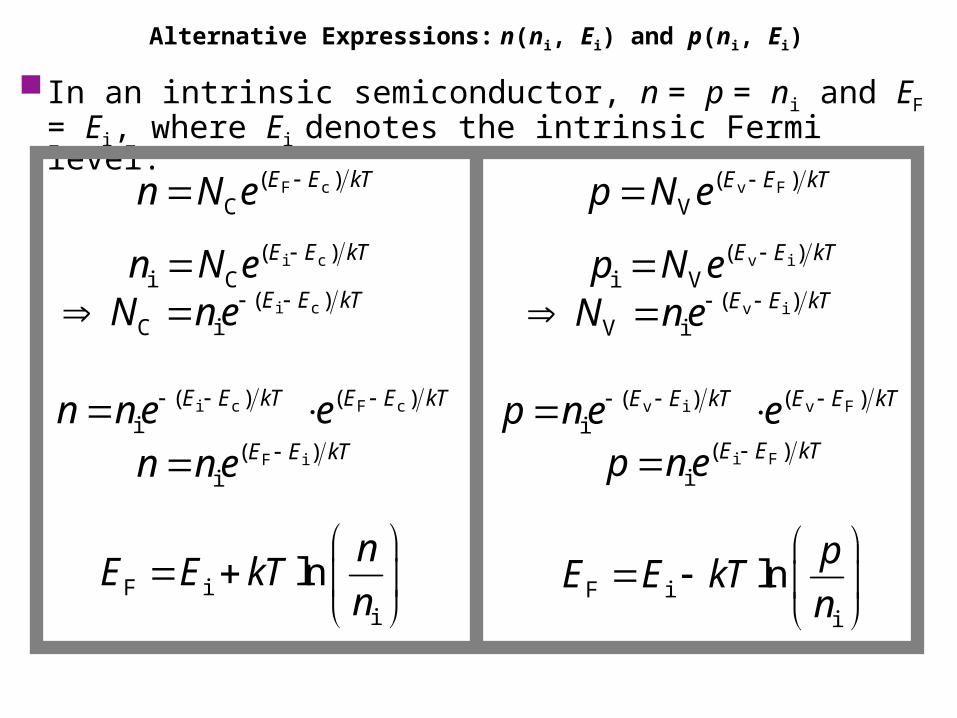
Boltzmann Approximation of Fermi Function In an intrinsic semiconductor, n = p = ni and EF = Ei, where Ei
denotes the intrinsic Fermi level.
v i v F( ) ( ) i
E E kT E E kTp n e e i c F c( ) ( )i
E E kT E E kTn n e e
F c( ) C
E E kTn N e
i F( )i
E E kTp n e
v F( )V
E E kTp N e
F i( )i
E E kTn n e
i c( ) C i
E E kTN n e
i c( ) i C
E E kTn N e
F ii
lnn
E E kTn
F i
i
lnp
E E kTn
v i( )i V
E E kTp N e v i( )
V iE E kTN n e
Alternative Expressions: n(ni, Ei) and p(ni, Ei)
Boltzmann Approximation of Fermi Functioni c v i( ) ( )
C VE E kT E E kTN e N e
c v Vi
C
ln2 2
E E NkTE
N
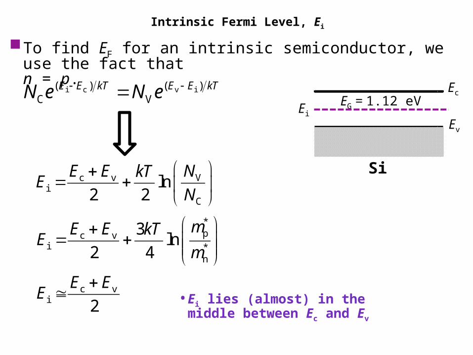
Ec
Ev
EG = 1.12 eV
Si
Ei
*pc v
i *n
3ln
2 4
mE E kTE
m
To find EF for an intrinsic semiconductor, we use the fact that n = p.
c vi 2
E EE
• Ei lies (almost) in the middle
between Ec and Ev
Intrinsic Fermi Level, Ei

Boltzmann Approximation of Fermi Function
175
10
100.56 8.62 10 300 ln eV
10
F ii
lnn
E E kTn
For Silicon at 300 K, where is EF if n = 1017 cm–3 ?
Silicon at 300 K, ni = 1010 cm–3
0.56 0.417 eV
0.977 eV
Example: Energy-Band Diagram

Boltzmann Approximation of Fermi Function
2i
D A 0, n
p n N N pn
ND: concentration of ionized donor (cm–3)NA: concentration of ionized acceptor (cm–3)?
Charge neutrality condition:
2i
D A 0n
n N Nn
2 2D A i( ) 0n n N N n
• Ei quadratic equation in n
Charge Neutrality and Carrier Concentration

Boltzmann Approximation of Fermi Function1 22
2D A D Ai2 2
N N N Nn n
1 222A D A Di2 2
N N N Np n
The solution of the previous quadratic equation for n is:
New quadratic equation can be constructed and the solution for p is:
• Carrier concentrations depend on net dopant concentration ND–NA or NA–ND
Charge-Carrier Concentrations
Boltzmann Approximation of Fermi Function
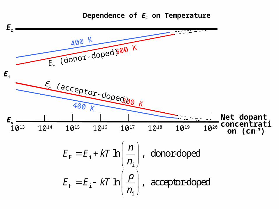
1013 1014 1015 1016 1017 1018 1019 1020
300 K400 K
400 K300 K
Net dopant concentration
(cm–3)
Ec
Ev
EF (donor-doped)
EF (acceptor-doped)
Ei
F ii
F ii
ln , donor-doped
ln , acceptor-doped
nE E kT
n
pE E kT
n
Dependence of EF on Temperature

Boltzmann Approximation of Fermi FunctionPhosphorus-doped Si
ND = 1015 cm–3
• n : number of majority carrier
• ND : number of donor electron
• ni : number of intrinsic conductive
electron
Carrier Concentration vs. Temperature

Boltzmann Approximation of Fermi Function
Three primary types of carrier action occur inside a semiconductor:Drift: charged particle motion in response to an applied
electric field.Diffusion: charged particle motion due to concentration
gradient or temperature gradient.Recombination-Generation: a process where charge
carriers (electrons and holes) are annihilated (destroyed) and created.
Carrier Action

Boltzmann Approximation of Fermi Function
123
4
5
electron
Mobile electrons and atoms in the Si lattice are always in random thermal motion. Electrons make frequent collisions with the vibrating atoms. “Lattice scattering” or “phonon scattering” increases with increasing
temperature. Average velocity of thermal motion for electrons: ~1/1000 x speed of
light at 300 K (even under equilibrium conditions).Other scattering mechanisms:
Deflection by ionized impurity atoms. Deflection due to Coulombic force between carriers or “carrier-carrier
scattering.” Only significant at high carrier concentrations.
The net current in any direction is zero, if no electric field is applied.
Carrier Scattering

Boltzmann Approximation of Fermi Function
12
3
45
electron
EF = –qE
When an electric field (e.g. due to an externally applied voltage) is applied to a semiconductor, mobile charge-carriers will be accelerated by the electrostatic force.
This force superimposes on the random motion of electrons.
Electrons drift in the direction opposite to the electric fieldè Current flows.
• Due to scattering, electrons in a semiconductor do not achieve constant velocity nor acceleration.
• However, they can be viewed as particles moving at a constant average drift velocity vd.
Carrier Drift

Boltzmann Approximation of Fermi Function
vd t All holes this distance back from the normal plane
vd t A All holes in this volume will cross the plane in a time t
p vd t A Holes crossing the plane in a time t
q p vd t A Charge crossing the plane in a time t
q p vd A Charge crossing the plane per unit time I (Ampere)
Þ Hole drift current
q p vd Current density associated with hole drift current J (A/m2)
Drift Current

Boltzmann Approximation of Fermi FunctionP|drift dqpv AI
P|drift dqpvJ
d pv E
P|drift pq p EJ
d nv E
N|drift nq n EJ
N|drift dqnvJ
For holes,
In low-field limit,
Similarly for electrons,
• Hole current due to drift
• Hole current density due to drift
• Electron current density due to drift
• μp : hole mobility
• μn : electron mobility
Hole and Electron Mobility
Boltzmann Approximation of Fermi Function
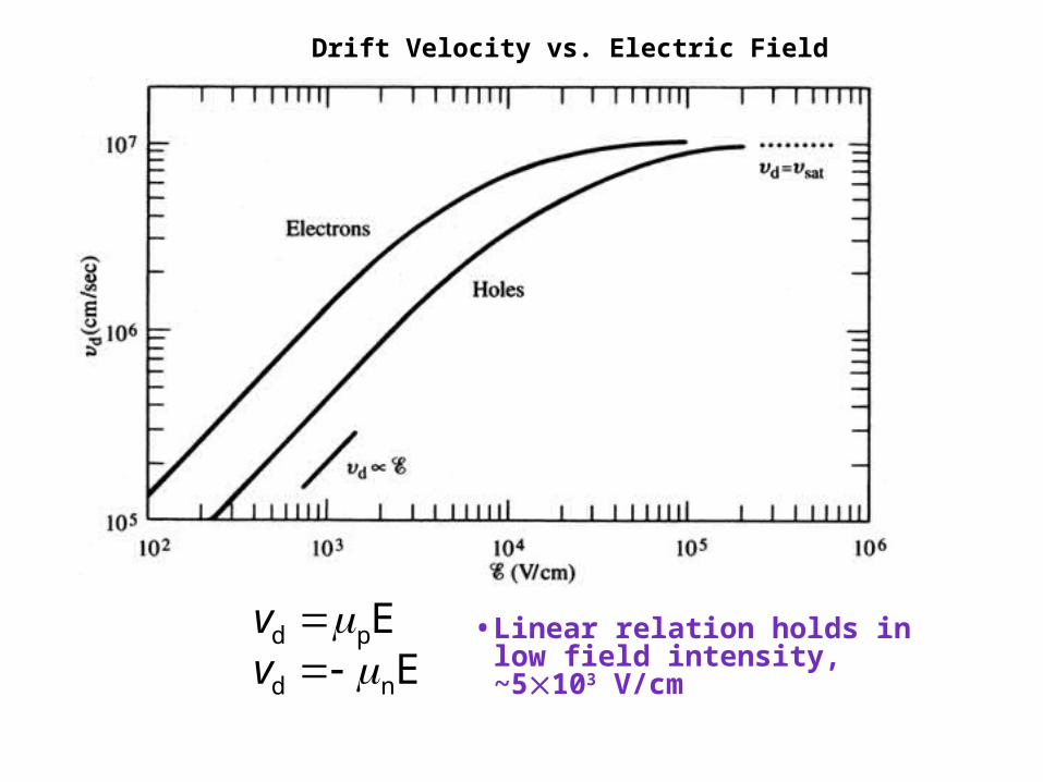
d pv E
d nv E• Linear relation holds in low field
intensity, ~5103 V/cm
Drift Velocity vs. Electric Field

Boltzmann Approximation of Fermi Function
Electron and hole mobility of selected intrinsic semiconductors (T = 300 K)
Si Ge GaAs InAs
n (cm2/V·s) 1400 3900 8500 30000
p (cm2/V·s) 470 1900 400 500
2cm/s cm
V/cm V s has the dimensions of v/E :
Hole and Electron Mobility
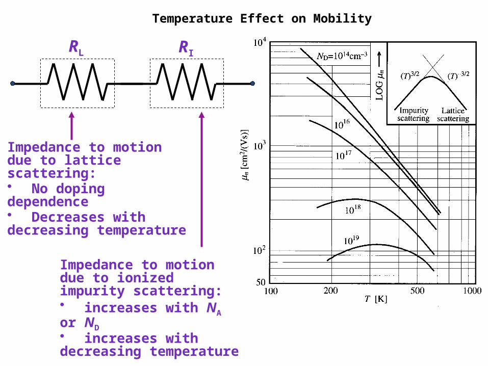
Boltzmann Approximation of Fermi FunctionRL RI
Impedance to motion due to lattice scattering:• No doping dependence• Decreases with
decreasing temperature
Impedance to motion due to ionized impurity scattering:• increases with NA or ND• increases with
decreasing temperature
Temperature Effect on Mobility

Boltzmann Approximation of Fermi Function
Carrier mobility varies with doping:Decrease with increasing total concentration of ionized
dopants.Carrier mobility varies with temperature:Decreases with increasing T if lattice scattering is
dominant.Decreases with decreasing T if impurity scattering is
dominant.
Temperature Effect on Mobility

Boltzmann Approximation of Fermi Function
JP|drift = qpvd = qppE
JN|drift = –qnvd = qnnE
Jdrift = JN|drift + JP|drift =q(nn+pp)E = E
Resistivity of a semiconductor: = 1 /
Conductivity of a semiconductor: = q(nn+pp)
Conductivity and Resistivity

Boltzmann Approximation of Fermi Function
D
1
nq N
A
1
pq N
For n-type material:
For p-type material:
Resistivity Dependence on Doping

Boltzmann Approximation of Fermi Function
n p
1
q n q p
Consider a Si sample at 300 K doped with 1016/cm3 Boron. What is its resistivity?
NA = 1016/cm3 , ND = 0 (NA >> ND p-type)
p 1016/cm3, n 104/cm3
119 16(1.6 10 )(470)(10 )
1.330 cm
p
1
q p
Example

Boltzmann Approximation of Fermi FunctionConsider a Si sample doped with 1017cm–3 As. How will its
resistivity change when the temperature is increased from T = 300 K to T = 400 K?
The temperature dependent factor in (and therefore ) is n. From the mobility vs. temperature curve for 1017cm–3, we find that n decreases from 770 at 300 K to 400 at 400 K.
As a result, increases by a factor of: 770/400 = 1.93
Example

Boltzmann Approximation of Fermi Function
Assignment


![Welcome to CDA Guwahati Portal!cdaguwahati.gov.in/docs/ANV-406-RECTT-CANTEENSTAFF-VOL-I...RAJAN KUMAR SINGH KUNDAN KUMAR GAURAV JANGRA ANU] KUMAR ANANT DC-WAN ASI-IVANI KUMAR NEKA](https://static.fdocuments.in/doc/165x107/601f18276168690b1d5154f8/welcome-to-cda-guwahati-portal-rajan-kumar-singh-kundan-kumar-gaurav-jangra.jpg)