Semiconductor Device Physics -...
28
1 Lecture 1 Semiconductor Device Physics http://zitompul.wordpress.com 2 0 1 3
Transcript of Semiconductor Device Physics -...
1
Lecture 1
Semiconductor Device Physics
http://zitompul.wordpress.com
2 0 1 3
2
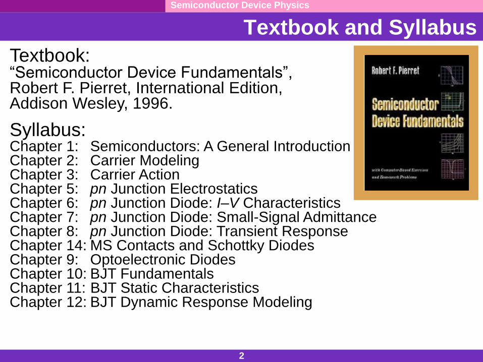
Textbook:“Semiconductor Device Fundamentals”, Robert F. Pierret, International Edition, Addison Wesley, 1996.
Textbook and Syllabus
Syllabus: Chapter 1: Semiconductors: A General IntroductionChapter 2: Carrier ModelingChapter 3: Carrier ActionChapter 5: pn Junction ElectrostaticsChapter 6: pn Junction Diode: I–V CharacteristicsChapter 7: pn Junction Diode: Small-Signal AdmittanceChapter 8: pn Junction Diode: Transient ResponseChapter 14: MS Contacts and Schottky Diodes Chapter 9: Optoelectronic DiodesChapter 10: BJT FundamentalsChapter 11: BJT Static CharacteristicsChapter 12: BJT Dynamic Response Modeling
Semiconductor Device Physics
3
References
The class materials are the Lecture note slides of the Semiconductor Device Physics course offered by Dr.-Ing. Erwin Sitompul, President University, Indonesia.
http://zitompul.wordpress.com/1-ee-lectures/2-semiconductor-device-physics/
Semiconductor Device Physics
4
Chapter 1Semiconductors: A General Introduction
Semiconductor Device Physics
5
Chapter 1 Semiconductors: A General Introduction
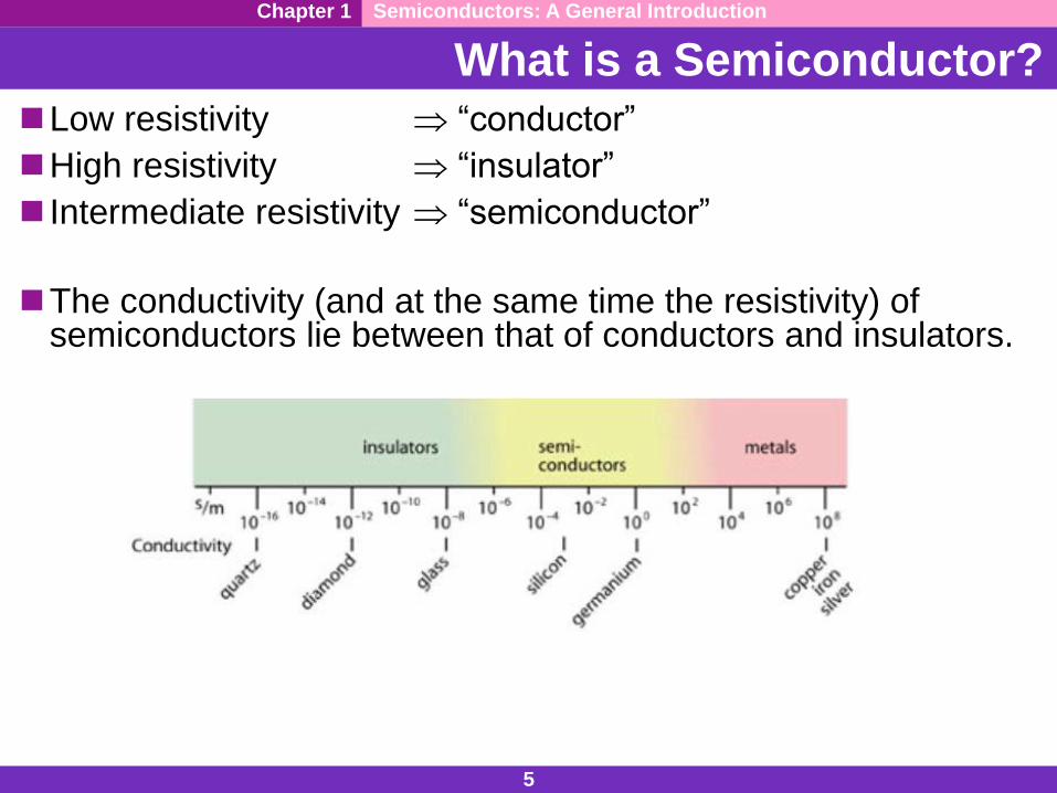
What is a Semiconductor?Low resistivity “conductor”
High resistivity “insulator”
Intermediate resistivity “semiconductor”
The conductivity (and at the same time the resistivity) of semiconductors lie between that of conductors and insulators.
6
No recognizable
long-range order
Completely ordered
in segments
Entire solid is made up of
atoms in an orderly
three- dimensional array
Chapter 1 Semiconductors: A General Introduction
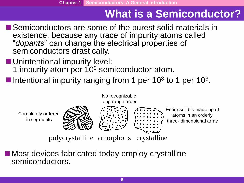
What is a Semiconductor?Semiconductors are some of the purest solid materials in
existence, because any trace of impurity atoms called “dopants” can change the electrical properties of semiconductors drastically.
Unintentional impurity level: 1 impurity atom per 109 semiconductor atom.
Intentional impurity ranging from 1 per 108 to 1 per 103.
Most devices fabricated today employ crystalline semiconductors.
polycrystalline amorphous crystalline
7
Semiconductor Materials
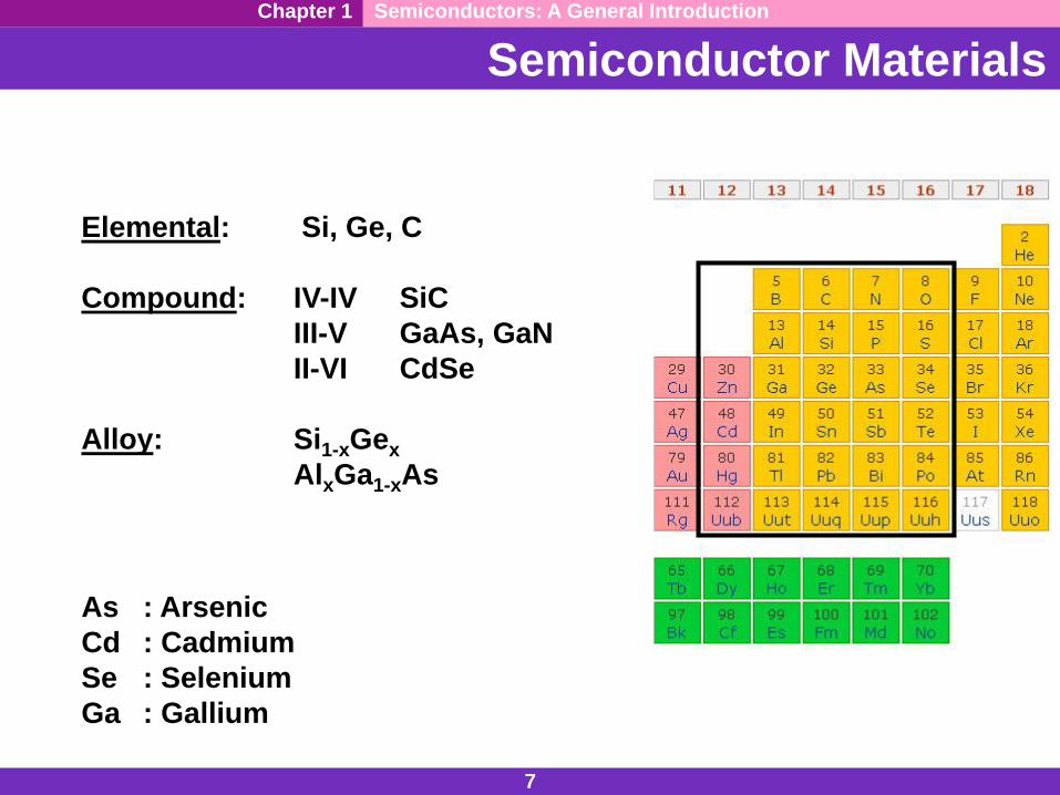
Elemental: Si, Ge, C
Compound: IV-IV SiC
III-V GaAs, GaN
II-VI CdSe
Alloy: Si1-xGex
AlxGa1-xAs
Chapter 1 Semiconductors: A General Introduction
As : Arsenic
Cd : Cadmium
Se : Selenium
Ga : Gallium
8
From Hydrogen to Silicon
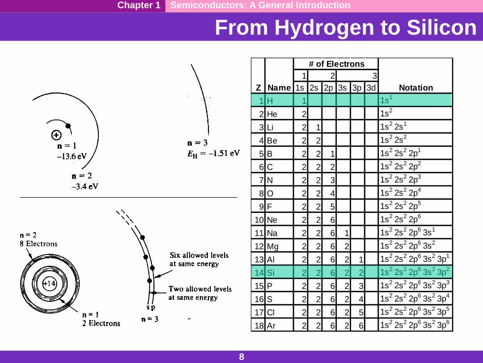
1
1s 2s 2p 3s 3p 3d
1 H 1 1s1
2 He 2 1s2
3 Li 2 1 1s2 2s1
4 Be 2 2 1s2 2s2
5 B 2 2 1 1s2 2s2 2p1
6 C 2 2 2 1s2 2s2 2p2
7 N 2 2 3 1s2 2s2 2p3
8 O 2 2 4 1s2 2s2 2p4
9 F 2 2 5 1s2 2s2 2p5
10 Ne 2 2 6 1s2 2s2 2p6
11 Na 2 2 6 1 1s2 2s2 2p6 3s1
12 Mg 2 2 6 2 1s2 2s2 2p6 3s2
13 Al 2 2 6 2 1 1s2 2s2 2p6 3s2 3p1
14 Si 2 2 6 2 2 1s2 2s2 2p6 3s2 3p2
15 P 2 2 6 2 3 1s2 2s2 2p6 3s2 3p3
16 S 2 2 6 2 4 1s2 2s2 2p6 3s2 3p4
17 Cl 2 2 6 2 5 1s2 2s2 2p6 3s2 3p5
18 Ar 2 2 6 2 6 1s2 2s2 2p6 3s2 3p6
Z Name Notation
2 3
# of Electrons
Chapter 1 Semiconductors: A General Introduction
9
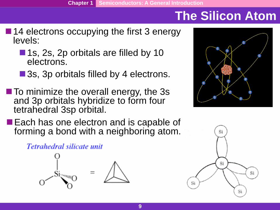
The Silicon Atom
Chapter 1 Semiconductors: A General Introduction
14 electrons occupying the first 3 energy levels:
1s, 2s, 2p orbitals are filled by 10 electrons.
3s, 3p orbitals filled by 4 electrons.
To minimize the overall energy, the 3s and 3p orbitals hybridize to form four tetrahedral 3sp orbital.
Each has one electron and is capable of forming a bond with a neighboring atom.
10
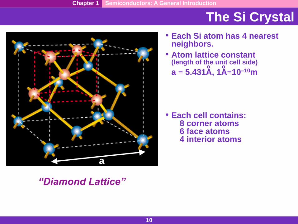
The Si Crystal
“Diamond Lattice”
a
Chapter 1 Semiconductors: A General Introduction
• Each Si atom has 4 nearest neighbors.
• Atom lattice constant(length of the unit cell side)
a = 5.431A, 1A=10–10m° °
• Each cell contains: 8 corner atoms6 face atoms4 interior atoms
11
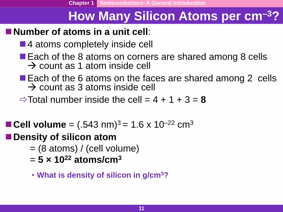
How Many Silicon Atoms per cm–3?
Chapter 1 Semiconductors: A General Introduction
Number of atoms in a unit cell:
4 atoms completely inside cell
Each of the 8 atoms on corners are shared among 8 cells count as 1 atom inside cell
Each of the 6 atoms on the faces are shared among 2 cells count as 3 atoms inside cell
Total number inside the cell = 4 + 1 + 3 = 8
Cell volume = (.543 nm)3 = 1.6 x 10⁻²² cm3
Density of silicon atom
= (8 atoms) / (cell volume)
= 5 × 10²² atoms/cm3
• What is density of silicon in g/cm3?

13
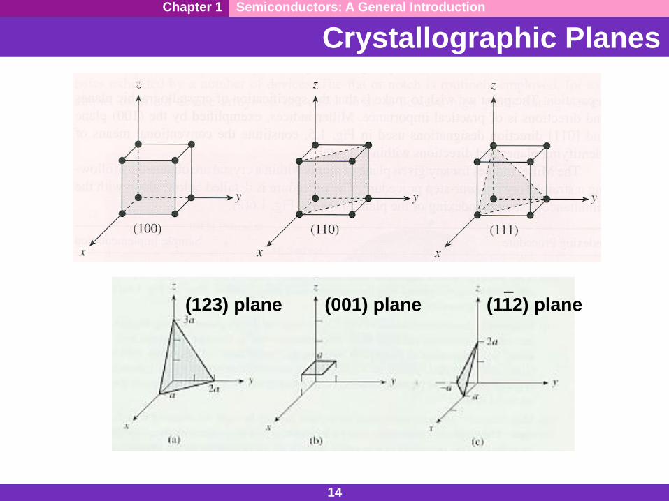
Crystallographic Notation
Notation Interpretation
( h k l ) crystal plane
{ h k l } equivalent planes
[ h k l ] crystal direction
< h k l > equivalent directions
h: inverse x-intercept of planek: inverse y-intercept of planel: inverse z-intercept of plane
(h, k and l are reduced to 3 integers having the same ratio.)
Miller Indices
Chapter 1 Semiconductors: A General Introduction
14
Crystallographic Planes
(123) plane (001) plane (112) plane
Chapter 1 Semiconductors: A General Introduction
_
15
Crystallographic Planes
Chapter 1 Semiconductors: A General Introduction
16
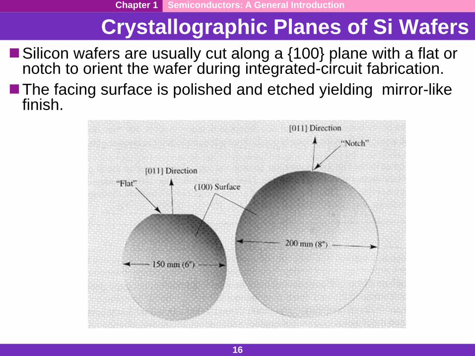
Crystallographic Planes of Si Wafers
Chapter 1 Semiconductors: A General Introduction
Silicon wafers are usually cut along a {100} plane with a flat or notch to orient the wafer during integrated-circuit fabrication.
The facing surface is polished and etched yielding mirror-like finish.
17
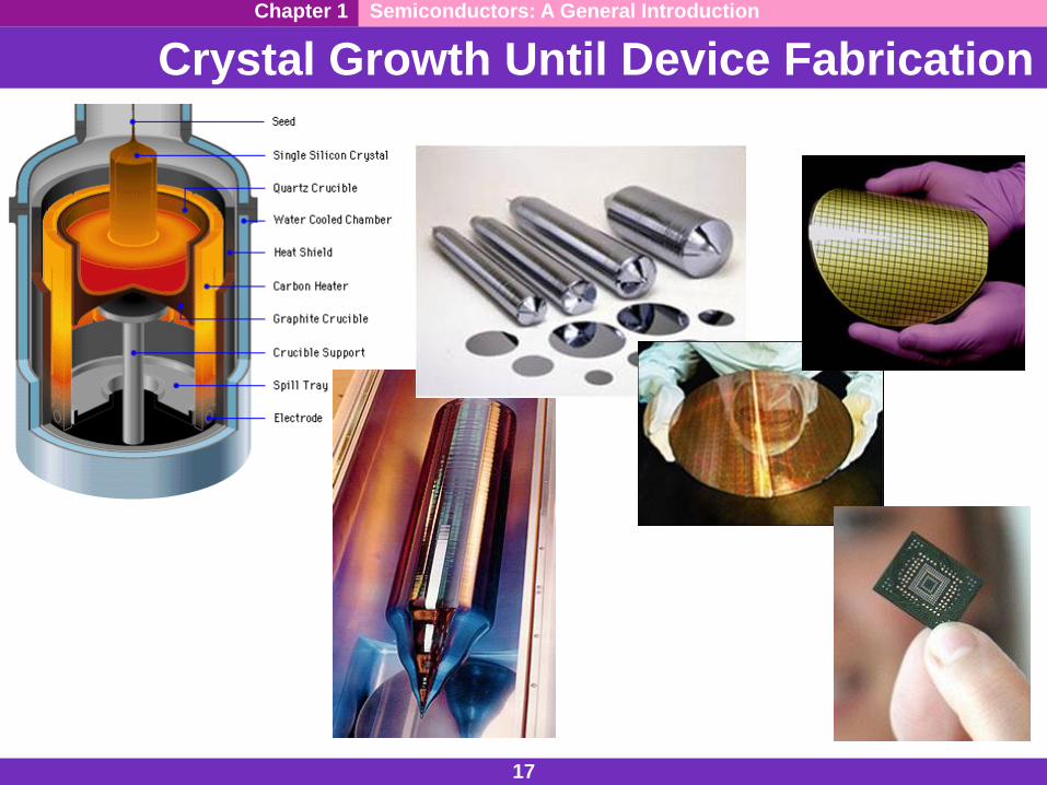
Crystal Growth Until Device Fabrication
Chapter 1 Semiconductors: A General Introduction
18
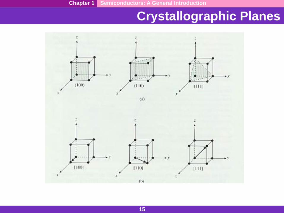
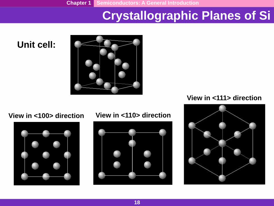
Unit cell:
View in <100> direction
Crystallographic Planes of Si
View in <110> direction
Chapter 1 Semiconductors: A General Introduction
View in <111> direction
19
Chapter 2Carrier Modeling
20
Chapter 2 Carrier Modeling
Electronic Properties of Si
Silicon is a semiconductor material.Pure Si has a relatively high electrical resistivity at room
temperature.
There are 2 types of mobile charge-carriers in Si:Conduction electrons are negatively charged,
e = –1.602 10–19 CHoles are positively charged,
p = +1.602 10–19 C
The concentration (number of atoms/cm3) of conduction electrons & holes in a semiconductor can be influenced in several ways:Adding special impurity atoms (dopants)Applying an electric fieldChanging the temperature Irradiation

21
Si Si Si
Si Si Si
Si Si Si
Si Si Si
Si Si Si
Si Si Si
Hole
Conduction
electron
Chapter 2 Carrier Modeling
Bond Model of Electrons and Holes
When an electron breaks loose and becomes a conduction electron, then a hole is created.
2-D Representation
22
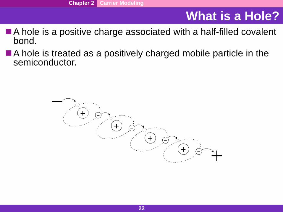
Chapter 2 Carrier Modeling
What is a Hole?A hole is a positive charge associated with a half-filled covalent
bond.
A hole is treated as a positively charged mobile particle in the semiconductor.

23
Chapter 2 Carrier Modeling
Conduction Electron and Hole of Pure Si
ni = intrinsic carrierconcentration
ni ≈ 1010 cm–3 at room temperature
• Covalent (shared e–) bonds exists between Si atoms in a crystal.
• Since the e– are loosely bound, some will be free at any T, creating hole-electron pairs.
24
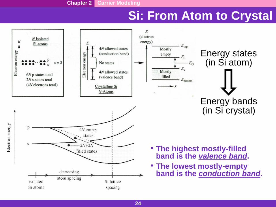
Energy states(in Si atom)
Chapter 2 Carrier Modeling
Si: From Atom to Crystal
• The highest mostly-filled band is the valence band.
• The lowest mostly-empty band is the conduction band.
Energy bands(in Si crystal)
25
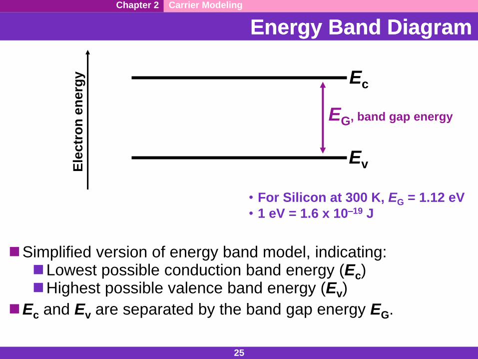
Ec
EvEle
ctr
on
en
erg
y
• For Silicon at 300 K, EG = 1.12 eV
• 1 eV = 1.6 x 10⁻¹⁹ J
EG, band gap energy
Chapter 2 Carrier Modeling
Energy Band DiagramEnergy Band Diagram
Simplified version of energy band model, indicating:Lowest possible conduction band energy (Ec)Highest possible valence band energy (Ev)
Ec and Ev are separated by the band gap energy EG.
26
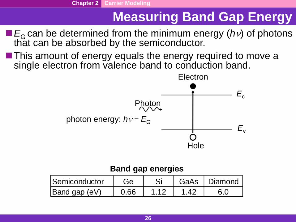
Band gap energies
Semiconductor Ge Si GaAs Diamond
Band gap (eV) 0.66 1.12 1.42 6.0
Chapter 2 Carrier Modeling
Measuring Band Gap EnergyEG can be determined from the minimum energy (hn) of photons
that can be absorbed by the semiconductor.
This amount of energy equals the energy required to move a single electron from valence band to conduction band.
Photon
photon energy: hn = EG
Ec
Ev
Electron
Hole
27
Carriers
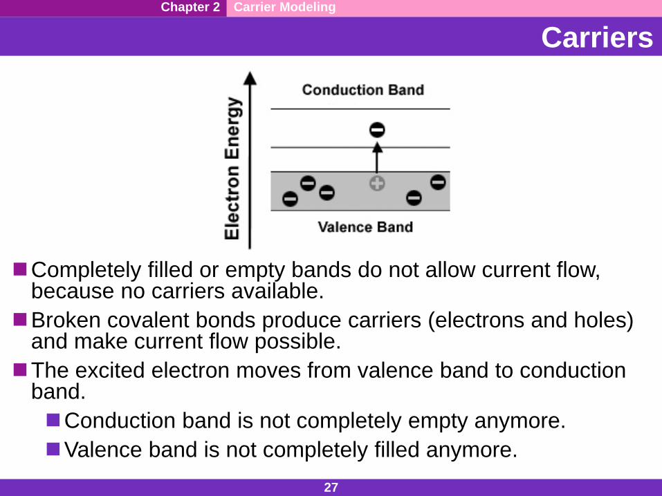
Chapter 2 Carrier Modeling
Completely filled or empty bands do not allow current flow, because no carriers available.
Broken covalent bonds produce carriers (electrons and holes) and make current flow possible.
The excited electron moves from valence band to conduction band.
Conduction band is not completely empty anymore.
Valence band is not completely filled anymore.
28
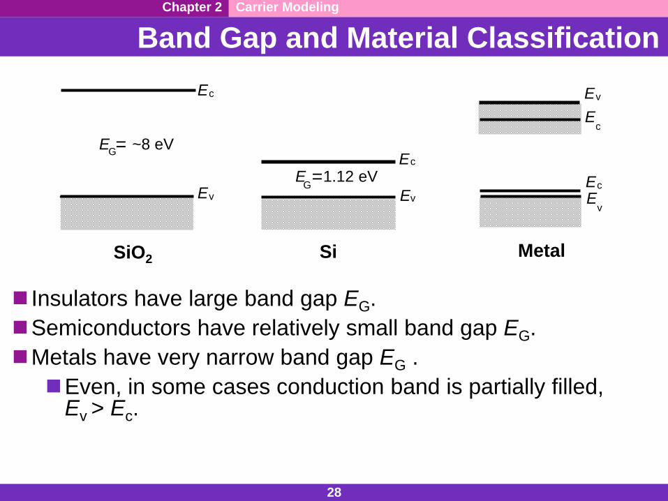
Band Gap and Material Classification
Ec
Ev
EG=1.12 eV
Si Metal
Ev
Ec
E
Ec
vEc
EG= ~8 eV
SiO2
Ev
Chapter 2 Carrier Modeling
Insulators have large band gap EG.
Semiconductors have relatively small band gap EG.
Metals have very narrow band gap EG .
Even, in some cases conduction band is partially filled,Ev > Ec.
29
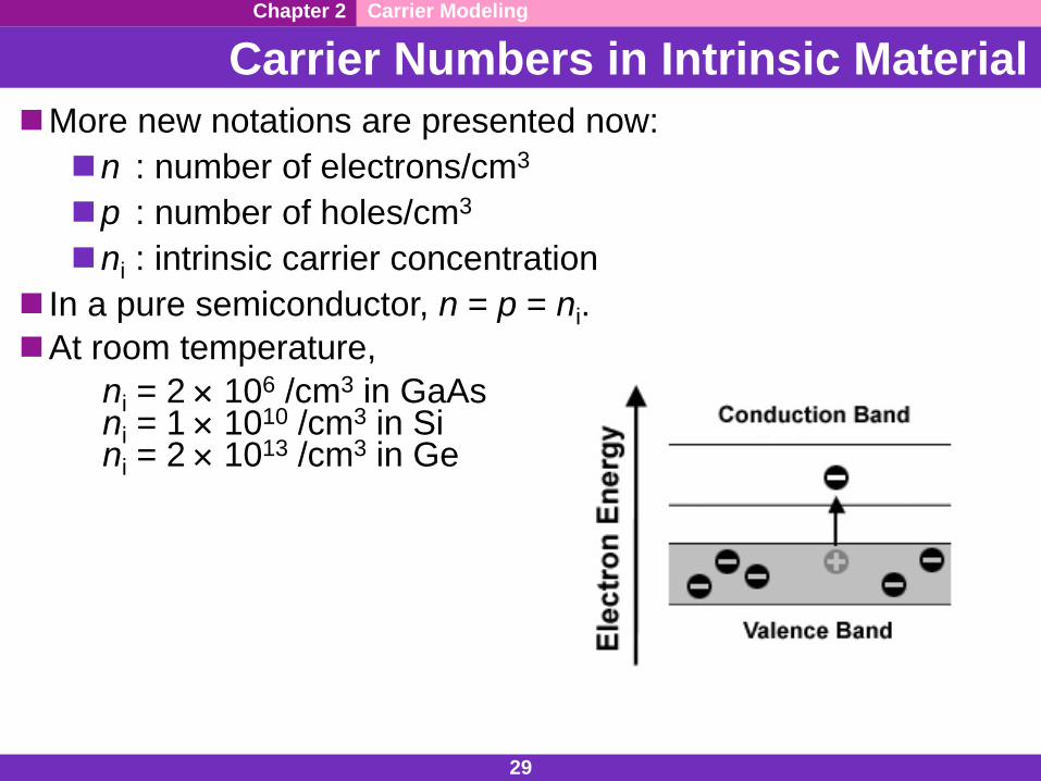
Carrier Numbers in Intrinsic Material
Chapter 2 Carrier Modeling
More new notations are presented now:
n : number of electrons/cm3
p : number of holes/cm3
ni : intrinsic carrier concentration
In a pure semiconductor, n = p = ni.
At room temperature,
ni = 2 106 /cm3 in GaAsni = 1 1010 /cm3 in Si ni = 2 1013 /cm3 in Ge