SEMICONDUCTOR AND DIODE
22
Semiconductors & Diodes 185 July 24 Name ___________________________ Date ____________ Partners____________________ ______________ SEMICONDUCTORS AND DIODES OBJECTIVES • To learn the basic properties of semiconductors and how their properties can be modified. • To understand the basic principles of a semiconducting diode. • To understand how the biasing properties of a p-n junction diode operate and how a diode might operate in a circuit. • To measure the IV curve of a diode. • To use the properties of a diode to rectify AC voltage. • To understand how LEDs operate. OVERVIEW Types of Conducting Materials. The electrical properties of materials can be divided into three broad categories: conductors, insulators, and semiconductors. In addition, a few materials exhibit superconductivity, but we will not address those here. Metals (both pure elements and alloys) are called conductors, because they typically conduct electricity. Materials like glass, Teflon, ceramics, and plastics are called insulators, because they are poor conductors of electricity. The third category, semiconductors, is the subject of this laboratory; their properties lie between conductors and insulators. Semiconductors are interesting, because we can control their electrical properties. Energy Bands. Let’s first examine the band theory of m aterials. Quantum physics indicates that electrons are placed in certain allowed energy levels in an atom. These are called shells (or orbitals) and subshells. From the Pauli Exclusion Principle, we know how the electrons are placed in the shells and subshells. The properties of the elements are primarily determined by the most loosely bound electrons, which are in the outside shells. Sometimes these outside electrons are tightly bound, and insulators result. If the outside electrons, called valence electrons, are only weakly bound, the electrons are fairly free to move around a solid consisting of many atoms. Thus the material is a conductor. When atoms come together to form molecules, the atomic energy levels overlap. When many atoms or molecules are placed together to form solids, the atomic energy levels become energy bands or just bands. The electrical properties of materials become clearer if we look at the University of Virginia Physics Department PHYS 636, Summer 2006
-
Upload
naren-rohit -
Category
Documents
-
view
220 -
download
5
Transcript of SEMICONDUCTOR AND DIODE
8/7/2019 SEMICONDUCTOR AND DIODE
http://slidepdf.com/reader/full/semiconductor-and-diode 1/22
Semiconductors & Diodes 185
July 24
Name ___________________________ Date ____________ Partners__________________________________
SEMICONDUCTORS AND DIODES
OBJECTIVES
• To learn the basic properties of semiconductors and how theirproperties can be modified.
• To understand the basic principles of a semiconducting diode.
• To understand how the biasing properties of a p-n junction diode
operate and how a diode might operate in a circuit.
• To measure the IV curve of a diode.
• To use the properties of a diode to rectify AC voltage.
• To understand how LEDs operate.
OVERVIEW
Types of Conducting Materials. The electrical properties of materials can be divided into three
broad categories: conductors, insulators, and semiconductors. In addition, a few materialsexhibit superconductivity, but we will not address those here. Metals (both pure elements and
alloys) are called conductors, because they typically conduct electricity. Materials like glass,Teflon, ceramics, and plastics are called insulators, because they are poor conductors of electricity. The third category, semiconductors, is the subject of this laboratory; their properties
lie between conductors and insulators. Semiconductors are interesting, because we can control
their electrical properties.
Energy Bands. Let’s first examine the band theory of materials. Quantum physics indicates
that electrons are placed in certain allowed energy levels in an atom. These are called shells (or
orbitals) and subshells. From the Pauli Exclusion Principle, we know how the electrons areplaced in the shells and subshells. The properties of the elements are primarily determined by
the most loosely bound electrons, which are in the outside shells. Sometimes these outside
electrons are tightly bound, and insulators result. If the outside electrons, called valenceelectrons, are only weakly bound, the electrons are fairly free to move around a solid consisting
of many atoms. Thus the material is a conductor.
When atoms come together to form molecules, the atomic energy levels overlap. When many
atoms or molecules are placed together to form solids, the atomic energy levels become energy
bands or just bands. The electrical properties of materials become clearer if we look at the
University of Virginia Physics Department
PHYS 636, Summer 2006
8/7/2019 SEMICONDUCTOR AND DIODE
http://slidepdf.com/reader/full/semiconductor-and-diode 2/22
186 Semiconductors & Diodes
July 24
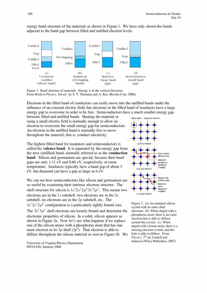
energy band structure of the materials as shown in Figure 1. We have only shown the bands
adjacent to the band gap between filled and unfilled electron levels.
Figure 1. Band structure of materials. Energy is in the vertical direction.
From Modern Physics, 3rd ed. by S. T. Thornton and A. Rex (Brooks Cole, 2006).
Electrons in the filled band of conductors can easily move into the unfilled bands under the
influence of an external electric field, but electrons in the filled band of insulators have a large
energy gap to overcome in order to be free. Semiconductors have a much smaller energy gapbetween filled and unfilled bands. Heating the material or
using a small electric field is normally enough to allow an
electron to overcome the small energy gap for semiconductors.
An electron in the unfilled band is normally free to movethroughout the material; that is, conduct electricity.
Figure 2. (a) An undoped silicon
crystal with its outer shell
electrons. (b) When doped with a
phosphorus atom, there is an extra
electron that is able to diffuse
around the crystal. (c) When
doped with a boron atom, there is a
missing electron or hole, and the
hole is able to diffuse. From
Physics, 7th ed, Cutnell and
Johnson (Wiley Publishers, 2007).
The highest filled band for insulators and semiconductors iscalled the valence band. It is separated by the energy gap from
the next (unfilled) band, normally referred to as the conduction
band. Silicon and germanium are special, because their bandgaps are only 1.11 eV and 0.66 eV, respectively, at room
temperature. Insulators typically have a band gap of about 3
eV, but diamond can have a gap as large as 6 eV.
We can see how semiconductors like silicon and germanium are
so useful by examining their intrinsic electron structure. The
shell structure for silicon is 1 2 . This means two
electrons are in the 1s subshell, two electrons are in the 2s
subshell, six electrons are in the 2p subshell, etc. Theconfiguration is a particularly tightly bound core.
The shell electrons are loosely bound and determine the
electronic properties of silicon. In a solid, silicon appears as
shown in Figure 2a. Now let’s see what happens if we replaceone of the silicon atoms with a phosphorus atom that has one
more electron in its 3p shell (3p
2 2 6 2 22 3 3s s p s p
2
2 2 61 2 2s s p23 3s p
3). That electron is able to
diffuse throughout the silicon material as seen in Figure 2b. We
University of Virginia Physics Department
PHYS 636, Summer 2006
8/7/2019 SEMICONDUCTOR AND DIODE
http://slidepdf.com/reader/full/semiconductor-and-diode 3/22
Semiconductors & Diodes 187
July 24
say that we have doped the intrinsic silicon semiconductor, and we call the result an n-type
doped semiconductor. We have produced an extrinsic semiconductor that has different electrical
properties because of the impure phosphorus atom and its extra electron. Most semiconductorsused in electronic circuits are of this extrinsic type.
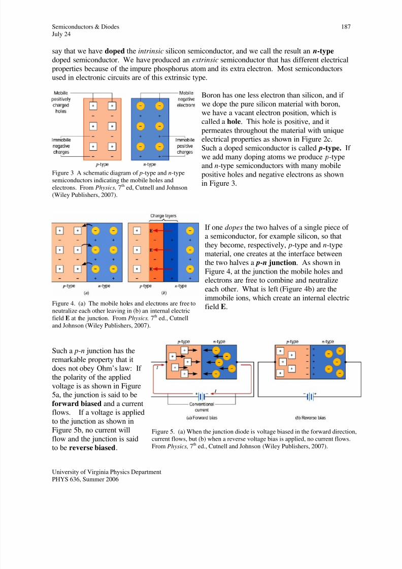
Figure 3 A schematic diagram of p-type and n-type
semiconductors indicating the mobile holes and
electrons. From Physics, 7th ed, Cutnell and Johnson
(Wiley Publishers, 2007).
Boron has one less electron than silicon, and if we dope the pure silicon material with boron,we have a vacant electron position, which is
called a hole. This hole is positive, and it
permeates throughout the material with uniqueelectrical properties as shown in Figure 2c.
Such a doped semiconductor is called p-type. If
we add many doping atoms we produce p-typeand n-type semiconductors with many mobile
positive holes and negative electrons as shown
in Figure 3.
Figure 4. (a) The mobile holes and electrons are free to
neutralize each other leaving in (b) an internal electric
field E at the junction. From Physics, 7th ed., Cutnell
and Johnson (Wiley Publishers, 2007).
If one dopes the two halves of a single piece of
a semiconductor, for example silicon, so that
they become, respectively, p-type and n-typematerial, one creates at the interface between
the two halves a p-n junction. As shown in
Figure 4, at the junction the mobile holes andelectrons are free to combine and neutralize
each other. What is left (Figure 4b) are theimmobile ions, which create an internal electric
field E.
Figure 5. (a) When the junction diode is voltage biased in the forward direction,
current flows, but (b) when a reverse voltage bias is applied, no current flows.
From Physics, 7th ed., Cutnell and Johnson (Wiley Publishers, 2007).
Such a p-n junction has the
remarkable property that itdoes not obey Ohm’s law: If
the polarity of the applied
voltage is as shown in Figure5a, the junction is said to be
forward biased and a currentflows. If a voltage is applied
to the junction as shown in
Figure 5b, no current will
flow and the junction is saidto be reverse biased.
University of Virginia Physics Department
PHYS 636, Summer 2006
8/7/2019 SEMICONDUCTOR AND DIODE
http://slidepdf.com/reader/full/semiconductor-and-diode 4/22
188 Semiconductors & Diodes
July 24
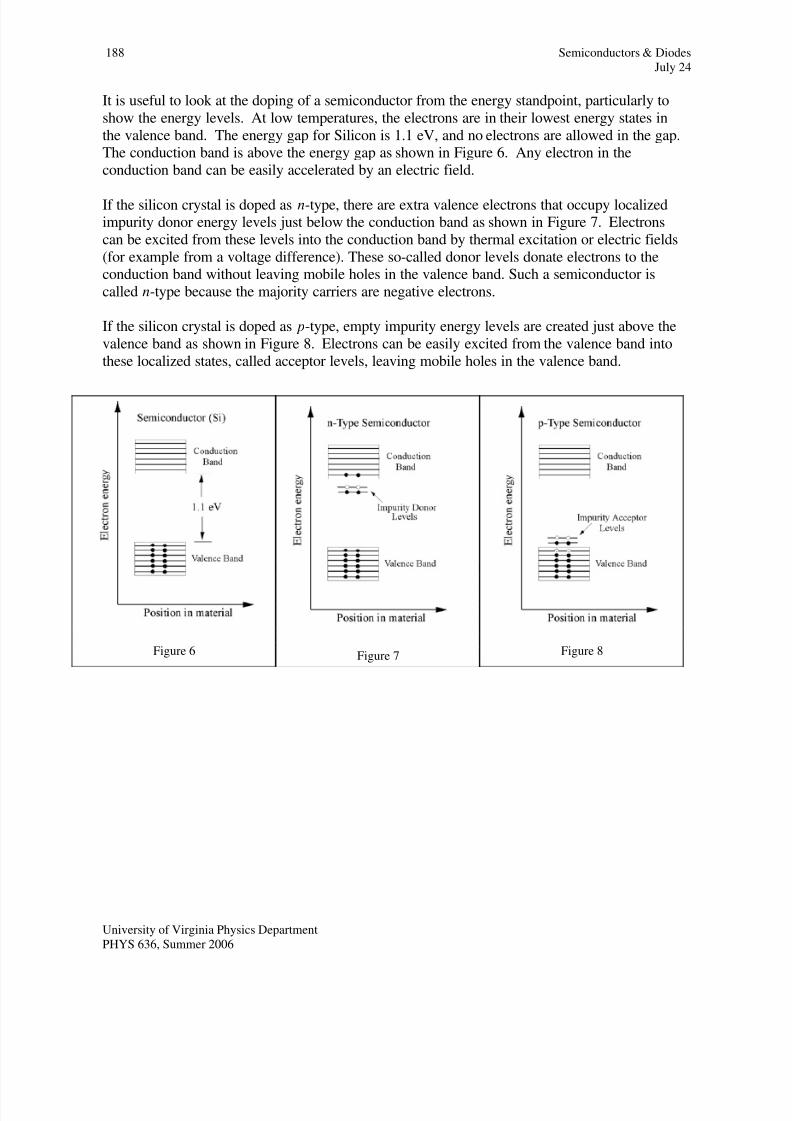
It is useful to look at the doping of a semiconductor from the energy standpoint, particularly to
show the energy levels. At low temperatures, the electrons are in their lowest energy states in
the valence band. The energy gap for Silicon is 1.1 eV, and no electrons are allowed in the gap.The conduction band is above the energy gap as shown in Figure 6. Any electron in the
conduction band can be easily accelerated by an electric field.
If the silicon crystal is doped as n-type, there are extra valence electrons that occupy localizedimpurity donor energy levels just below the conduction band as shown in Figure 7. Electrons
can be excited from these levels into the conduction band by thermal excitation or electric fields
(for example from a voltage difference). These so-called donor levels donate electrons to theconduction band without leaving mobile holes in the valence band. Such a semiconductor is
called n-type because the majority carriers are negative electrons.
If the silicon crystal is doped as p-type, empty impurity energy levels are created just above the
valence band as shown in Figure 8. Electrons can be easily excited from the valence band into
these localized states, called acceptor levels, leaving mobile holes in the valence band.
Figure 6 Figure 7 Figure 8
University of Virginia Physics Department
PHYS 636, Summer 2006
8/7/2019 SEMICONDUCTOR AND DIODE
http://slidepdf.com/reader/full/semiconductor-and-diode 5/22
Semiconductors & Diodes 189
July 24
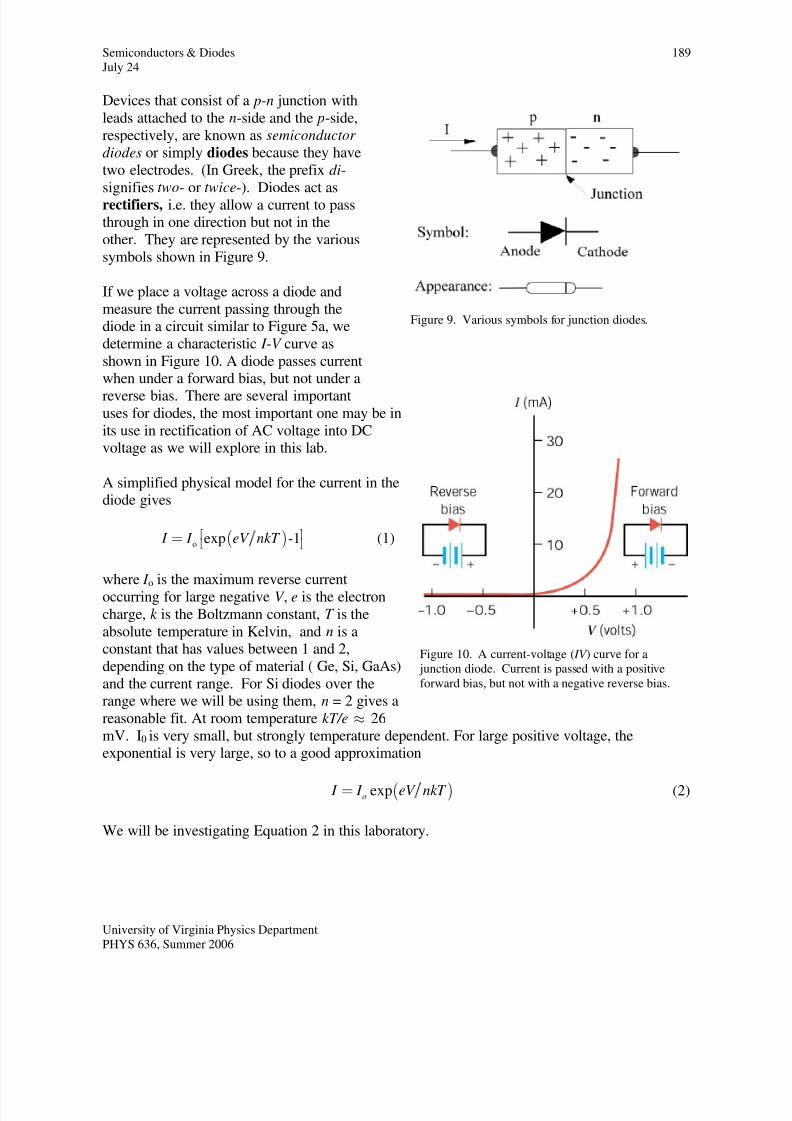
Devices that consist of a p-n junction with
leads attached to the n-side and the p-side,
respectively, are known as semiconductor
diodes or simply diodes because they have
two electrodes. (In Greek, the prefix di-
signifies two- or twice-). Diodes act asrectifiers, i.e. they allow a current to passthrough in one direction but not in the
other. They are represented by the various
symbols shown in Figure 9.
If we place a voltage across a diode and
measure the current passing through thediode in a circuit similar to Figure 5a, we
determine a characteristic I -V curve as
shown in Figure 10. A diode passes current
when under a forward bias, but not under areverse bias. There are several important
uses for diodes, the most important one may be in
its use in rectification of AC voltage into DCvoltage as we will explore in this lab.
A simplified physical model for the current in thediode gives
( )o exp -1I I eV nkT ⎡=⎣
⎤⎦
(1)
where I o is the maximum reverse currentoccurring for large negative V , e is the electron
charge, k is the Boltzmann constant, T is the
absolute temperature in Kelvin, and n is aconstant that has values between 1 and 2,
depending on the type of material ( Ge, Si, GaAs)
and the current range. For Si diodes over therange where we will be using them, n = 2 gives a
reasonable fit. At room temperature kT/e 26
mV. I
≈
0 is very small, but strongly temperature dependent. For large positive voltage, theexponential is very large, so to a good approximation
Figure 9. Various symbols for junction diodes.
Figure 10. A current-voltage (IV ) curve for a
junction diode. Current is passed with a positive
forward bias, but not with a negative reverse bias.
( )expoI I eV nk = T (2)
We will be investigating Equation 2 in this laboratory.
University of Virginia Physics Department
PHYS 636, Summer 2006
8/7/2019 SEMICONDUCTOR AND DIODE
http://slidepdf.com/reader/full/semiconductor-and-diode 6/22
190 Semiconductors & Diodes
July 24
INVESTIGATION 1: DIODE PROPERTIES
In this investigation you will be given a diode and asked to determine
its properties. Which way is voltage applied for the forward bias?
How can you tell the p- type end of a diode from the n-type end? Andfinally you will measure the voltage-current (the so-called IV curve) of
a diode to show that it does not have ohmic characteristics, that is, it
does not follow ohm’s law.
In order to do this you will need the following items:
• a 1N914 diode
• Wavetek 27XT multimeter
• D-cell battery and holder
• several wires with alligator clips
• 1000 Ω resistor
Activity 1-1: Diode Direction
1. Use the material listed above to determine the correct direction that
current will flow through the diode. Use the black circle around the
diode to define the orientation of the diode.
Remember that ammeters have small internal resistances that are not equal on
different current scales. Voltmeters have large internal resistances. You may want
to consider this while doing this experiment.
2. Discuss the method by which you made your determination. Use
simple drawings if necessary.
University of Virginia Physics Department
PHYS 636, Summer 2006
8/7/2019 SEMICONDUCTOR AND DIODE
http://slidepdf.com/reader/full/semiconductor-and-diode 7/22
Semiconductors & Diodes 191
July 24
Question 1-1: Which end of the diode is the p-type and n-type? Use
the black circle around the diode as a reference. Discuss how you know
this.
In electronics we normally refer to the + voltage side as the anode
and the – voltage side as the cathode. When using cables we
sometimes use red cables for +voltage and black cables for –volta e or ground .
Question 1-2: Is the black circle end of the diode the anode or cathodeend when positive voltage allows current to pass through? Explain how
you determined this?
Activity 1-2: IV Curve
In this activity you will determine the current-voltage (IV ) curve for ajunction diode. Remember to not exceed a few mA (certainly no more
than 20 mA) through the silicon diode.
In addition to the material used in the previous activity, you will need
the following:
• Op amp designer board
• Several connecting wires to use with the board
• Data Studio computer system
Never exceed 8.0 volts across the diode! If you destroy a diode,
points will be deducted from your lab grade. It is actually the
current through the diode that is crucial. Don’t exceed 20 mA.
University of Virginia Physics Department
PHYS 636, Summer 2006
8/7/2019 SEMICONDUCTOR AND DIODE
http://slidepdf.com/reader/full/semiconductor-and-diode 8/22
192 Semiconductors & Diodes
July 24
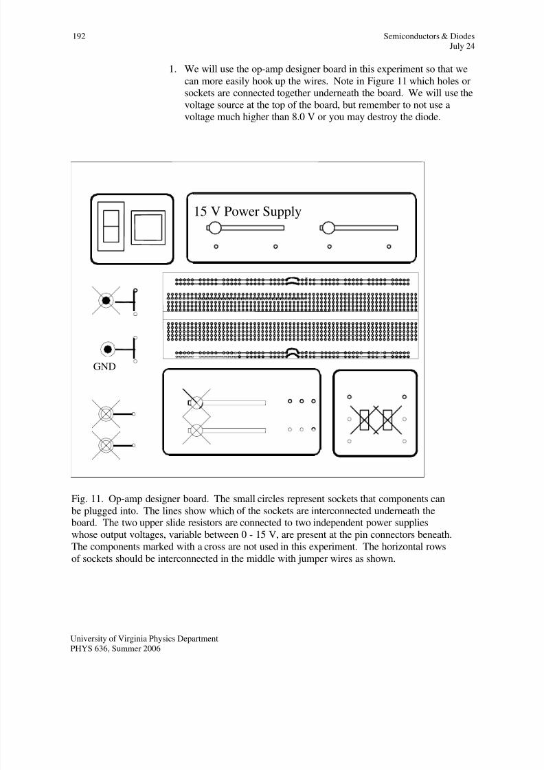
1. We will use the op-amp designer board in this experiment so that we
can more easily hook up the wires. Note in Figure 11 which holes or
sockets are connected together underneath the board. We will use thevoltage source at the top of the board, but remember to not use a
voltage much higher than 8.0 V or you may destroy the diode.
GND
15 V Power Supply
GND
ig. 11. Op-amp designer board. The small circles represent sockets that components canF
be plugged into. The lines show which of the sockets are interconnected underneath theboard. The two upper slide resistors are connected to two independent power supplies
whose output voltages, variable between 0 - 15 V, are present at the pin connectors beneath.
The components marked with a cross are not used in this experiment. The horizontal rows
of sockets should be interconnected in the middle with jumper wires as shown.
University of Virginia Physics Department
PHYS 636, Summer 2006

8/7/2019 SEMICONDUCTOR AND DIODE
http://slidepdf.com/reader/full/semiconductor-and-diode 9/22
Semiconductors & Diodes 193
July 24
2. Assemble the circuit shown in Figure 12. Connect the negative
terminal of the power supply (one of the 0 – 15 V supplies at the top
of the board) to the ground terminal to reduce noise. The ground isthe black connector on the left of the board.
3. Note that the voltage read at input B is proportional to the current
through the diode (I = V/R) and is numerically the value of thecurrent in mA, because we are reading the voltage across a 1.0 k Ω
resistor.
Figure 12. Circuit to produce IV curve for diode.
1 k Ω
0 - 15 V VR
input B
input AVdiode
+-
to PASCO
red black
to PASCO
red
black
4. Open the experiment file Diode IV in Data Studio.
5. The computer will record 20 samples per second of the voltages at A
and B and list them in the two tables. A graph of B input(proportional to current) will be plotted versus the A input (voltage
across the diode).
6. Start recording data and slowly slide the voltage knob and increasethe voltage from 0 to about 8 volts. You will feel a click in the slider
as you reach this voltage. Stop recording. You have obtained data for
the positive voltages. Do not erase the data.
7. Determine the value of voltage at which the graph is going almost
straight up. You will probably find it is 0.6 – 0.7 V.
Voltage: _____________
8. Now you need to make a similar plot but using negative voltages.You can do this by reversing the two leads on the power supply,
setting the supply to –8V, start recording, sweep up to 0 V. This will
be a new run, but the data will be plotted on the same graph as thepositive voltages (but in a different color on the screen).
University of Virginia Physics Department
PHYS 636, Summer 2006
8/7/2019 SEMICONDUCTOR AND DIODE
http://slidepdf.com/reader/full/semiconductor-and-diode 10/22
194 Semiconductors & Diodes
July 24
Question 1-3: Does the graph have the qualitative shape you expect
from the previous discussion? Discuss.
Question 1-4: What threshold voltage did you find for silicon? Is thisabout what you expected? Discuss.
Question 1-5: Did you detect any current passing through the diodewhen the bias voltage was negative (reverse bias)? If so, what was it?
Current ______________________
How can you explain the existence of this current?
9. Print out a copy of your graph for your group report. You do not
need to print out the data tables. Do not erase your data!
Activity 1-3: Determination of n in Equation 2
We now want to compare your data for positive voltages with Equation2. You should be able to do this by using the fit data routines of Data
Studio, which you have done previously.
1. Arrange for your graph to show only the positive voltage data.
2. Now figure out a way to fit these data with an exponential. Describehere how you did this and list the best value of the exponential term
e/nkT .
University of Virginia Physics Department
PHYS 636, Summer 2006
8/7/2019 SEMICONDUCTOR AND DIODE
http://slidepdf.com/reader/full/semiconductor-and-diode 11/22
Semiconductors & Diodes 195
July 24
Best fit value of e/nkT with uncertainty _______________
Question 1-6: Did the visual fit of your data lead you to believe thatEquation 2 describes the diode’s behavior? Discuss.
3. Use the known values of e and k and the room temperature T anddetermine the value of n.
n: _________
Question 1-7: Is this value of n consistent with what you expected?
Discuss.
4. Ask your Instructor if time is available to repeat this activity for a
germanium diode (Sylvania #ECG109). If time is available, give the
values for germanium below:
Threshold voltage: _____________
n: _________
Question 1-8: Are these values consistent with what you expect forgermanium? Discuss.
University of Virginia Physics Department
PHYS 636, Summer 2006
8/7/2019 SEMICONDUCTOR AND DIODE
http://slidepdf.com/reader/full/semiconductor-and-diode 12/22
196 Semiconductors & Diodes
July 24
Activity 1-4: Diode Test Function on Wavetek Multimeter
Many good multimeters have a test function to determine the forward
bias voltage of a given diode. Our Wavetek model 27XT has such afunction.
1. Turn the switch on the Wavetek to the symbol. Connect the
red test lead to the V-Ω input and the black test lead to the COM
input.
2. Connect the probe tip of the red test lead to the anode and the black test lead to the cathode of the diode.
3. The meter applies just enough voltage to allow current to pass. The
meter’s display indicates the forward voltage drop.
4. Reverse the test leads on the diode to perform a reverse bias test. An
overload signal ( OL) indicates a good diode.
An overload condition for both reverse and forward bias testsindicates an open diode, which means the diode is bad. A low
voltage reading for both bias tests indicates a shorted diode.
5. Perform the forward and reverse bias tests for both a silicon and
germanium diode. List your results below:
Silicon bias voltage: _____________________
Germanium bias voltage: _________________
INVESTIGATION 2: RECTIFICATION OF AC VOLTAGE
In this investigation you will investigate the use of diodes in rectifying
AC voltage, for example from AC to DC. The uses of rectifiers are toonumerous to mention, but the electrical generator of your automobilemost likely produces AC voltage that must be rectified to DC for your
car’s electrical system. Calculators and computers also use rectifiers.
In addition to the material used in the previous activity, you will need the
following:
University of Virginia Physics Department
PHYS 636, Summer 2006
8/7/2019 SEMICONDUCTOR AND DIODE
http://slidepdf.com/reader/full/semiconductor-and-diode 13/22
Semiconductors & Diodes 197
July 24
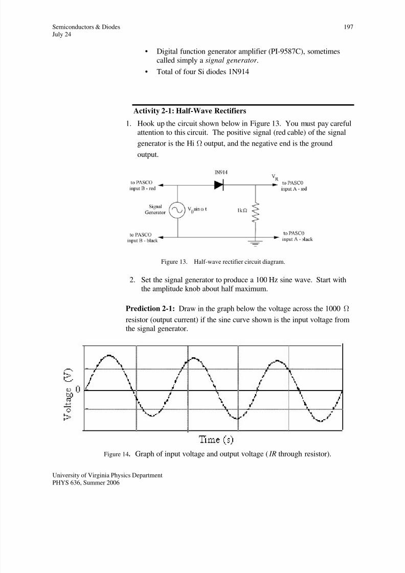
• Digital function generator amplifier (PI-9587C), sometimes
called simply a signal generator .
• Total of four Si diodes 1N914
Activity 2-1: Half-Wave Rectifiers
1. Hook up the circuit shown below in Figure 13. You must pay careful
attention to this circuit. The positive signal (red cable) of the signal
generator is the Hi Ω output, and the negative end is the ground
output.
Figure 13. Half-wave rectifier circuit diagram.
2. Set the signal generator to produce a 100 Hz sine wave. Start with
the amplitude knob about half maximum.
Prediction 2-1: Draw in the graph below the voltage across the 1000 Ω
resistor (output current) if the sine curve shown is the input voltage fromthe signal generator.
Figure 14. Graph of input voltage and output voltage (IR through resistor).
University of Virginia Physics Department
PHYS 636, Summer 2006
8/7/2019 SEMICONDUCTOR AND DIODE
http://slidepdf.com/reader/full/semiconductor-and-diode 14/22
198 Semiconductors & Diodes
July 24
3. In Data Studio open the experiment file called Rectifier. Data
Studio will be in the oscilloscope mode, and you will be observingthe input signal generator voltage in Channel B and the current
through the diode (actually the voltage across the 1000 Ω resistor) in
channel A.
4. Start recording data. You should be triggering with channel B, the
signal generator. Make sure channel B is highlighted with the box
around it in the upper right of the computer screen (click on it tomake it happen). You will notice a green triangle on the left side of
the screen that denotes the triggering level (only voltage signals
above the trigger level pass through). Move the trigger level to seewhat happens.
5. You can set the amplitude of the input voltage by changing the
amplitude knob on the signal generator. Set the voltage to 4.0 V.You probably should have Data Studio set at 1 V/div on the vertical
screen and 2 ms/div on the horizontal. Change those values to see
what happens.
6. Use the Smart Tool in Data Studio to determine the maximum
voltage for the two cases.
Maximum input voltage ___________________________
Maximum output voltage (actually IR) _______________
7. Print out the data for your group report.
Question 2-1: Compare your data with your prediction. Discuss theagreement and explain any disagreement.
Question 2-2: Note in step 6 that the maximum output voltage was less
than the input voltage. Explain why.
University of Virginia Physics Department
PHYS 636, Summer 2006
8/7/2019 SEMICONDUCTOR AND DIODE
http://slidepdf.com/reader/full/semiconductor-and-diode 15/22
Semiconductors & Diodes 199
July 24
Question 2-3: Note that there is a time delay between the time the input
voltage rises above zero and the time the output voltage rises above zero.Explain why this occurs.
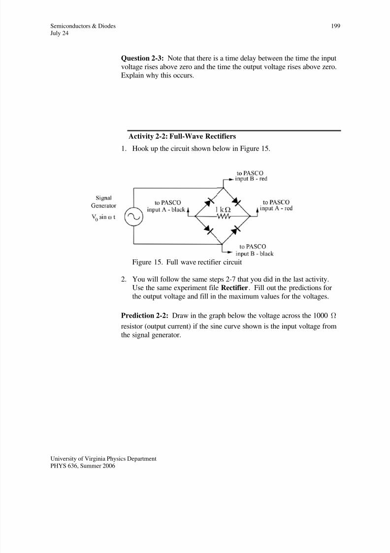
Activity 2-2: Full-Wave Rectifiers
1. Hook up the circuit shown below in Figure 15.
Figure 15. Full wave rectifier circuit
. You will follow the same steps 2-7 that you did in the last activity.
Prediction 2-2: Draw in the graph below the voltage across the 1000 Ω
2Use the same experiment file Rectifier. Fill out the predictions for
the output voltage and fill in the maximum values for the voltages.
resistor (output current) if the sine curve shown is the input voltage from
the signal generator.
University of Virginia Physics Department
PHYS 636, Summer 2006
8/7/2019 SEMICONDUCTOR AND DIODE
http://slidepdf.com/reader/full/semiconductor-and-diode 16/22
200 Semiconductors & Diodes
July 24
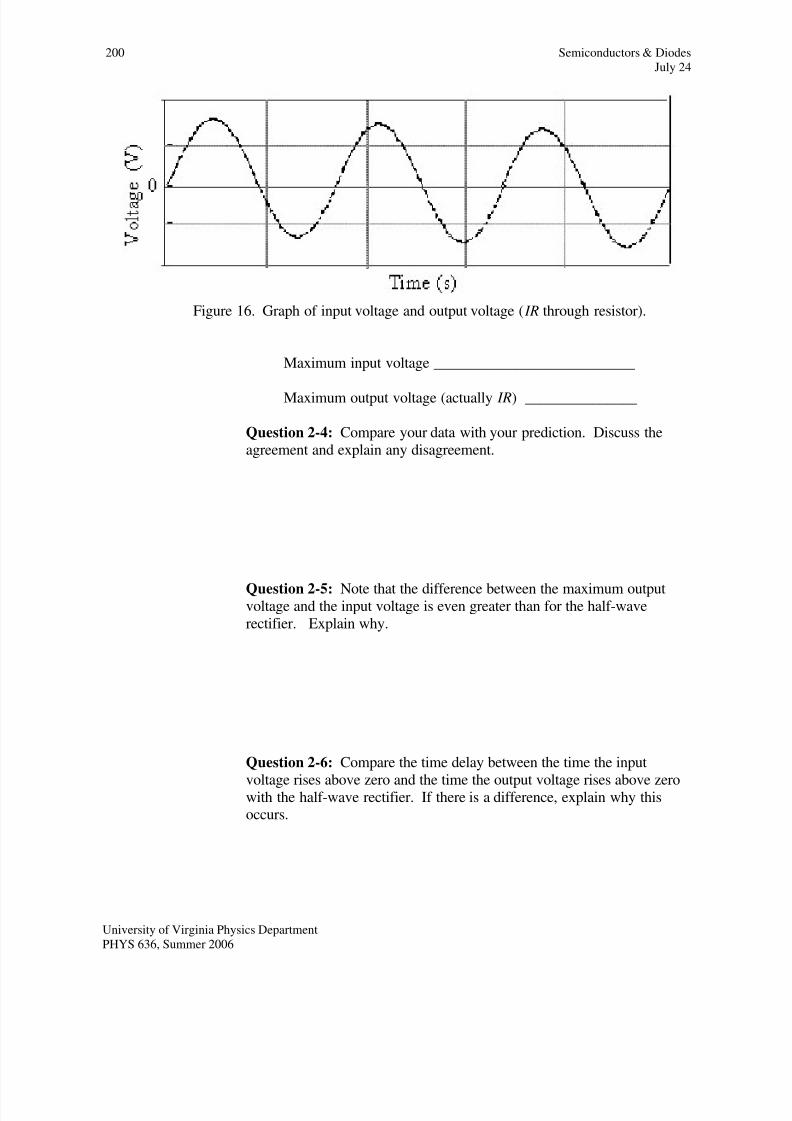
Figure 16. Graph of input voltage and output voltage (IR through resistor).
Maximum input voltage ___________________________
Maximum output voltage (actually IR) _______________
Question 2-4: Compare your data with your prediction. Discuss the
agreement and explain any disagreement.
Question 2-5: Note that the difference between the maximum output
voltage and the input voltage is even greater than for the half-wave
rectifier. Explain why.
Question 2-6: Compare the time delay between the time the inputvoltage rises above zero and the time the output voltage rises above zero
with the half-wave rectifier. If there is a difference, explain why thisoccurs.
University of Virginia Physics Department
PHYS 636, Summer 2006

8/7/2019 SEMICONDUCTOR AND DIODE
http://slidepdf.com/reader/full/semiconductor-and-diode 17/22
Semiconductors & Diodes 201
July 24
3. On the circuit diagram in Figure 15, draw the path that the current
takes through the rectifier circuit when the input voltage is positive.
Use a dashed line to draw the path that the current takes through therectifier circuit when the input voltage is negative. Make sure your
paths are clear and well marked.
Question 2-7: Explain why the output voltage across the 1000 Ω resistor
is always positive for the full wave rectifier.
INVESTIGATION 3: LIGHT EMITTING DIODES (LED)
Light emitting diodes are used in numerous applications including smallstore-front signs, digital clocks, remote controls for TVs and other
electronic devices, indication of electronic instruments and appliancesbeing on, road construction barrier lights, traffic signal illumination,
motorcycle/bicycle warning lights, spoiler and car decorative lights, etc.
You may even have one of the newer type flashlights that uses LEDs ordrive a car that uses LEDs for the turn or brake signals. Their advantages
are they don’t have a filament that burns out, they don’t get very hot, and
they last longer than incandescent bulbs.
As free electrons pass across the junction in a diode, they fall into empty
holes in the p-type material. When doing so, the electrons fall into alower energy level, and light in the form of electromagnetic radiationcalled photons is released. In the case of the silicon and germanium
crystals we have been studying up to now, those photons are in the
infrared spectrum, and they are not visible to the human eye. However,if the electron flow occurs in a junction diode with a larger energy band
gap, then the photons will be in the visible region. It is the energydifference that the electron experiences as it travels across the junction
that determines the photon frequency. The equation is
E hf = (3)
where f is the photon frequency, and h is Planck’s constant (value h =6.6261 x 10⁻³⁴ J s).
Scientists have developed such crystals to use as LEDs with compounds(using especially gallium) that produce visible light, such as
• aluminum gallium arsenide (AlGaAs) - red
University of Virginia Physics Department
PHYS 636, Summer 2006

8/7/2019 SEMICONDUCTOR AND DIODE
http://slidepdf.com/reader/full/semiconductor-and-diode 18/22
202 Semiconductors & Diodes
July 24
• aluminum gallium phosphide (AlGaP) - green
• aluminum gallium indium phosphide (AlGaInP) - orange, yellow,
and green
• gallium arsenide phosphide (GaAsP) - red, orange, and yellow
• gallium phosphide (GaP) - red, yellow and green
There is a huge advantage in efficiency by using LEDs compared with
incandescent bulbs where the filament must be very hot. LEDs do notproduce much heat. A much larger percentage of the electrical power
goes to produce light for LEDs as compared with incandescent bulbs.
The problem, until recently, has been the cost of producing LEDs. LEDshave become so inexpensive and reliable that they are taking over many
of the applications previously dominated by incandescent and fluorescent
bulbs. LEDs can last tens of thousands of hours and tend to be immuneto heat, cold, shock, and vibration. They do not have the annoying
flicker like from fluorescents, and scientists are still developing nice,
warm feeling white light that people prefer. The white LEDs nowavailable tend to have a little blue color in them. No breakable glass is
used in LEDs, and they can be waterproofed for marine use.
The circuit symbol for LEDs is
Figure 17. Diagram of a LED
showing the anode and cathode(K) leads.
The long lead wire is labeled anode for +. The short lead wire is
labeled k for cathode (after the German spelling kathode) and is
negative. There may be a slight flat on the body of round LEDs onthe cathode side. Most LEDs have colored bodies to enhance the
color, but we are using clear ones so we can more easily see thecolor of the light produced.
Never connect a battery or power supply directly across a LED. The diode may be
destroyed because of excessive current. LEDs must always be placed in series with a
resistor to limit the current. It is usually safe to place a 1 k Ω resistor in series.
Figure 18 shows a circuit in which the function of the
LED can be tested. V S is the supply voltage, R is the
resistor in series, and V L is the voltage across the LED.If I is the current through the circuit, we can write
Ohm’s law across the resistor as
voltage across resistor
or
(4)
R
R S L
S L
V
V IR V V
V V R
I
=
= = −
−=
Figure 18. Always place a resistor in series
with a LED before placing a voltage across
it.University of Virginia Physics Department
PHYS 636, Summer 2006
8/7/2019 SEMICONDUCTOR AND DIODE
http://slidepdf.com/reader/full/semiconductor-and-diode 19/22
Semiconductors & Diodes 203
July 24
Generally data sheets for LEDs tell us what maximum current should pass through the LED.
The range of voltages V L that trigger the LED we are using is about 2.0 volts. They can go up to4 V for blue or white LEDs.
You may need the following material:
• Digital function generator amplifier (PI-9587C), sometimes
called simply a signal generator .
• Op amp designer board
• Red, green, and yellow LEDs
• Three 1000 Ω resistors
• Several connecting wires to use with the board
Activity 3-1: LED Operation
Most LEDs come in colored covers to help enhance the color produced,but we are using clear cover LEDs so we can tell what color light is
produced.
Prediction 3-1: If our power supply has a maximum of 15 V, and theforward maximum voltages are about 2.5 V, calculate the value of the
resistor we should use for a limiting current of 20 mA.
Question 3-1: Will we be safe by using a 1 k Ω resistor in series with our
LEDs? Explain your answer.
Question 3-2: We want to test red, yellow, and green LEDs in one
circuit, but the voltages at which they pass current will probably be
University of Virginia Physics Department
PHYS 636, Summer 2006

8/7/2019 SEMICONDUCTOR AND DIODE
http://slidepdf.com/reader/full/semiconductor-and-diode 20/22
204 Semiconductors & Diodes
July 24
different. Do we want to place the three LEDs in series or parallel in
order to measure the voltages at which the LEDs pass current? Explain.
1. We want to determine the IV curves for the three LEDs. You mightwant to refer to Activity 1-2 and Figure 12. Draw the circuit below
you plan to use to test the LEDs. Before actually hooking up the
LEDs in your circuit, check with your instructor. Remember that a 1
k Ω resistor must be in series.
2. Use the op amp designer board to hook up your circuit after yourinstructor has approved your design. Use the 15 V sliding power
supply on the board.
3. Open the Data Studio experiment file DIODE IV that you usedpreviously in Activity 1-2. We want to determine the IV curve for
each LED in turn. When you are sure your circuit will not destroy the
LED, start data collection and turn up the voltage steadily until youreach 5 mA. You should see the diode light up. It is probably best to
stop the data collection before turning the voltage down, because the
data will retrace itself making it look messy. Do it again until youhave clean data. Find the voltage at which you first have 1 mA and
also 2 mA and put your results in Table 1.
Voltage (V)
Color 1 mA 2 mA
Red
Green
Yellow
University of Virginia Physics Department
PHYS 636, Summer 2006
8/7/2019 SEMICONDUCTOR AND DIODE
http://slidepdf.com/reader/full/semiconductor-and-diode 21/22
Semiconductors & Diodes 205
July 24
4. Repeat step 3 for the other two LEDs.
Question 3-3: From the energy relation, E = hf , does the order of voltage make sense? Which color has the largest frequency? Which
color has the largest energy band gap?
Activity 3-2: LED Oscillating Operation
Your assignment is to design and produce a circuit that shows a green
and red oscillating LED for which you can adjust the frequency of itgoing on and off. The green and red LEDs must each be on about half
the time, but not at the same time. You can use any of the equipment you
have available.
1. Draw the circuit below.
2. Remember that points will be deducted from everyone in your group
if you destroy a LED. Work together and make sure everyone agrees
about your circuit.
3. Show your instructor that your circuit works.
Question 3-4: What key operation did you have to do in order to have
the green and red LED oscillate out of phase?
University of Virginia Physics Department
PHYS 636, Summer 2006

8/7/2019 SEMICONDUCTOR AND DIODE
http://slidepdf.com/reader/full/semiconductor-and-diode 22/22
206 Semiconductors & Diodes
July 24
University of Virginia Physics Department