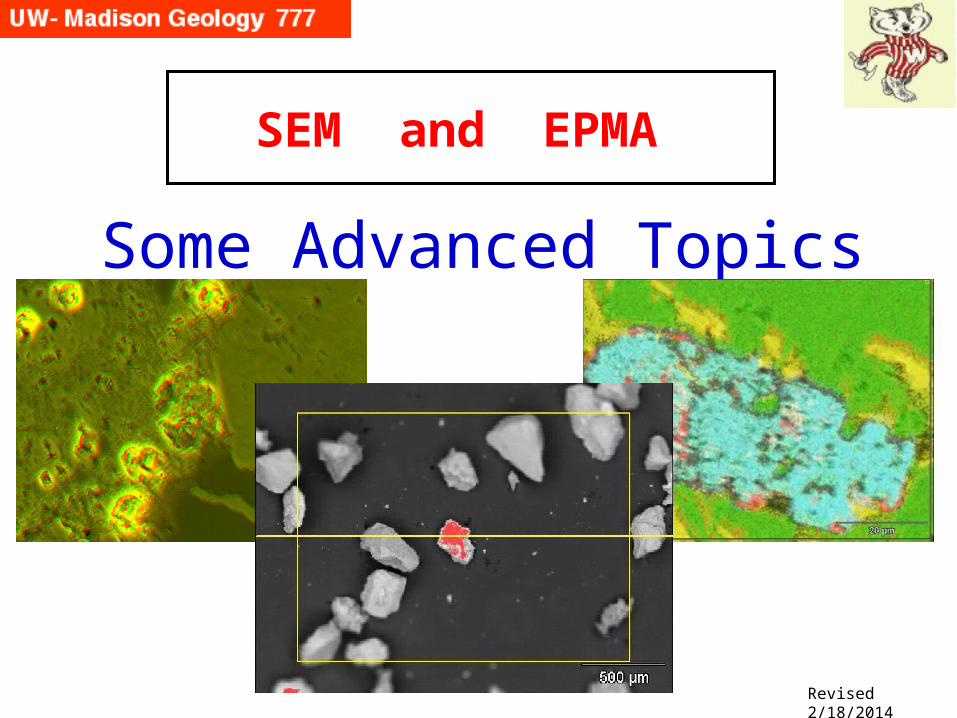
SEM and EPMA Some Advanced Topics Revised 2/18/2014.
37
SEM and EPMA Some Advanced Topics Revised 2/18/2014
-
Upload
griselda-mccarthy -
Category
Documents
-
view
220 -
download
3
Transcript of SEM and EPMA Some Advanced Topics Revised 2/18/2014.
SEM and EPMA
Some Advanced Topics
Revised 2/18/2014
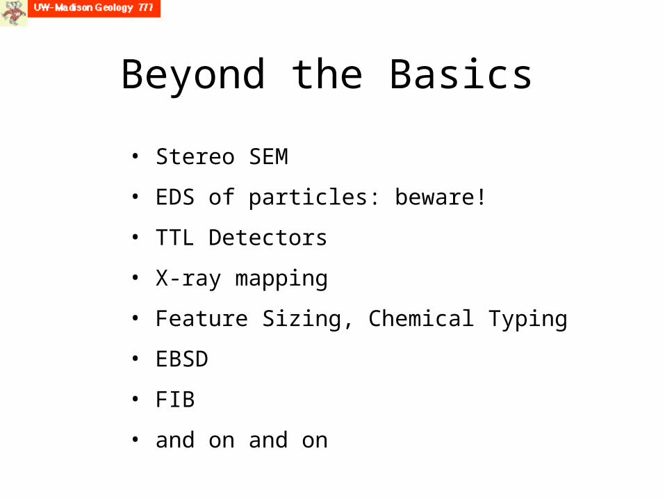
Beyond the Basics
• Stereo SEM
• EDS of particles: beware!
• TTL Detectors
• X-ray mapping
• Feature Sizing, Chemical Typing
• EBSD
• FIB
• and on and on

Stereo SEMWhy? Graphical demonstration of 3D
shapes of rough or complex objects
How? Very generally …..
1. Acquire two SEM images of the same object at the same magnification but by tilting the stage slightly.
2. Color each image red or green in Photoshop.
3. Then in Photoshop overlay the two images, while wearing red-green stereo glasses, shift them slightly apart until you have the correct 3D effect.
4. Show downstairs in 2nd floor visualization lab for maximum effect…
Exact detailed instructions on wall in room 308
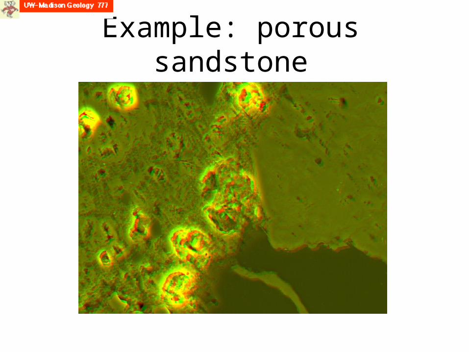
Example: porous sandstone
Stereo SEM Details
For rough objects, use 3-7° tilt
For smooth objects, use more, 7-15°
Use less tilt if higher magnification
If you need to refocus, do NOT change objective lense setting, rather move sample stage Z up or down.
Cited reference in literature: Heuser, 1989, Protocol for 3-D visualization of molecules on mica via the quick-freeze, deep-etch technique, Journal of Electron Microscopy Technique, vol 13, p. 244-263.
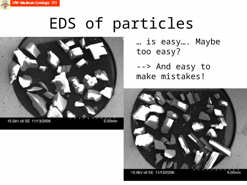
EDS of particles… is easy…. Maybe too easy?
--> And easy to make mistakes!
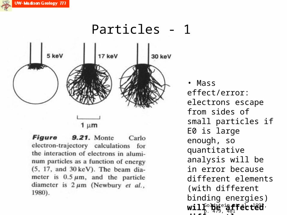
Particles - 1
• Mass effect/error: electrons escape from sides of small particles if E0 is large enough, so quantitative analysis will be in error because different elements (with different binding energies) will be affected differently
Goldstein et al, 1992, p. 479, 481
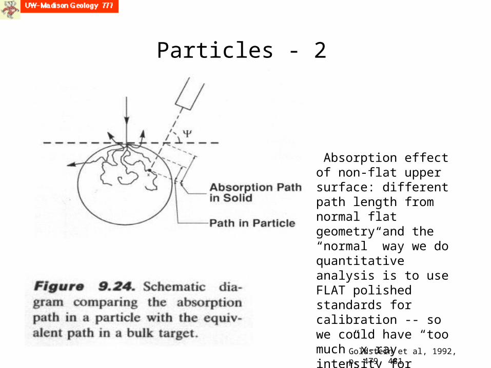
Particles - 2
Absorption effect of non-flat upper surface: different path length from normal flat geometry and the “normal” way we do quantitative analysis is to use FLAT polished standards for calibration -- so we could have “too much” x-ray intensity for particles
Goldstein et al, 1992, p. 479, 481

Particles - 3
•Variable effect of geometry of trajectory between beam impact area on non-uniform surface and the location of the detector -- so we get different results from the same material, depending upon where we place the electron beam.
Goldstein et al, 1992, p. 479, 481

Results from 2006 777 student project on EDS of rough samples with VP-SEM
The first column shows the actual chemical composition, followed by the average composition of 20 points on different grains, followed by the variation (=standard deviation) of those individual measurements
EDS X-ray Mapping-1
BSE imaging provides rapid distinction of some/many/most chemically distinct phases in a multiphase sample.
However, in many cases, having explicit 2D chemical information is value. This is where “x-ray mapping” comes into play.
X-ray mapping has changed tremendously since it was first introduced in 1956 as a combination of WDS (crystal diffraction spectrometry) and SEM: in those days it was called “dot mapping” as literally dots would be painted onto the CRT. To capture it, a photograph would have to be snapped of the screen. It generally was pretty grainy. And only 1 or 2 or 3 elements could be acquired simultaneously (depending on how many spectrometers were on the electron probe).

EDS X-ray Mapping-2
EDS was developed in the late 1960s and soon began to be used for X-ray mapping.
For the next 30 years or so, users would select “regions of interest” (ROIs), essentially the peak areas of particular elements -- sometimes limited to a finite value like 8 or 12 -- which would then be used to “color in” a 2D area over which the beam would scan, either one very long and slow scan, or many faster scans that would be averaged.
Note: To this point, all the above maps included both the characteristic X-ray being chosen AND the background/ continuum under the characteristic peak.
EDS X-ray Mapping-3Things have changed in the 40 years since
EDS came on the scene:
1. Digital pulse processing have taken over from the older analog processing, making shorter time constants and thus higher count rates possible (e.g. 30,000 cps vs 3,000 cps before) which create many more opportunities -- larger areas, shorter times.
2. And then the development of SDD (Si-Drift Detectors) have boosted the count rates to the hundreds of thousands of cps.
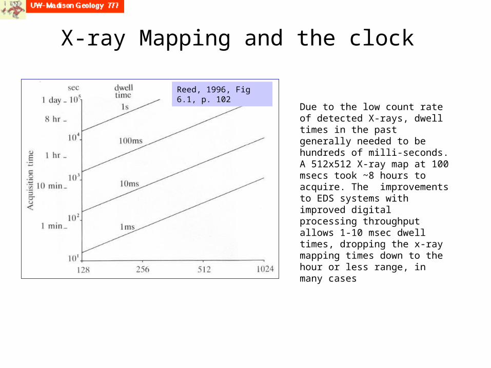
X-ray Mapping and the clock
Due to the low count rate of detected X-rays, dwell times in the past generally needed to be hundreds of milli-seconds. A 512x512 X-ray map at 100 msecs took ~8 hours to acquire. The improvements to EDS systems with improved digital processing throughput allows 1-10 msec dwell times, dropping the x-ray mapping times down to the hour or less range, in many cases
Reed, 1996, Fig 6.1, p. 102
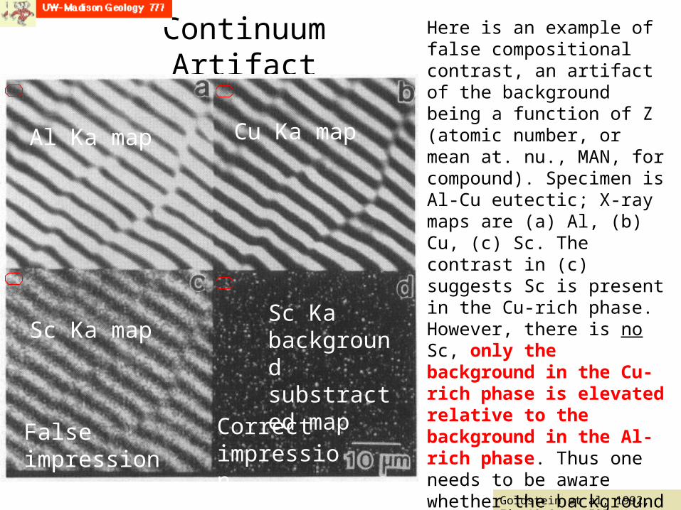
Continuum Artifact
Goldstein et al, 1992, Fig 10.6, p. 535
Here is an example of false compositional contrast, an artifact of the background being a function of Z (atomic number, or mean at. nu., MAN, for compound). Specimen is Al-Cu eutectic; X-ray maps are (a) Al, (b) Cu, (c) Sc. The contrast in (c) suggests Sc is present in the Cu-rich phase. However, there is no Sc, only the background in the Cu-rich phase is elevated relative to the background in the Al-rich phase. Thus one needs to be aware whether the background is or is not subtracted from X-ray maps, esp. when looking at minor elements where the continuum is a major component. Many published maps do not state if bkg-subtracted, so assume they aren’t.
False impression
Correct impression
Al Ka map Cu Ka map
Sc Ka mapSc Ka background substracted map
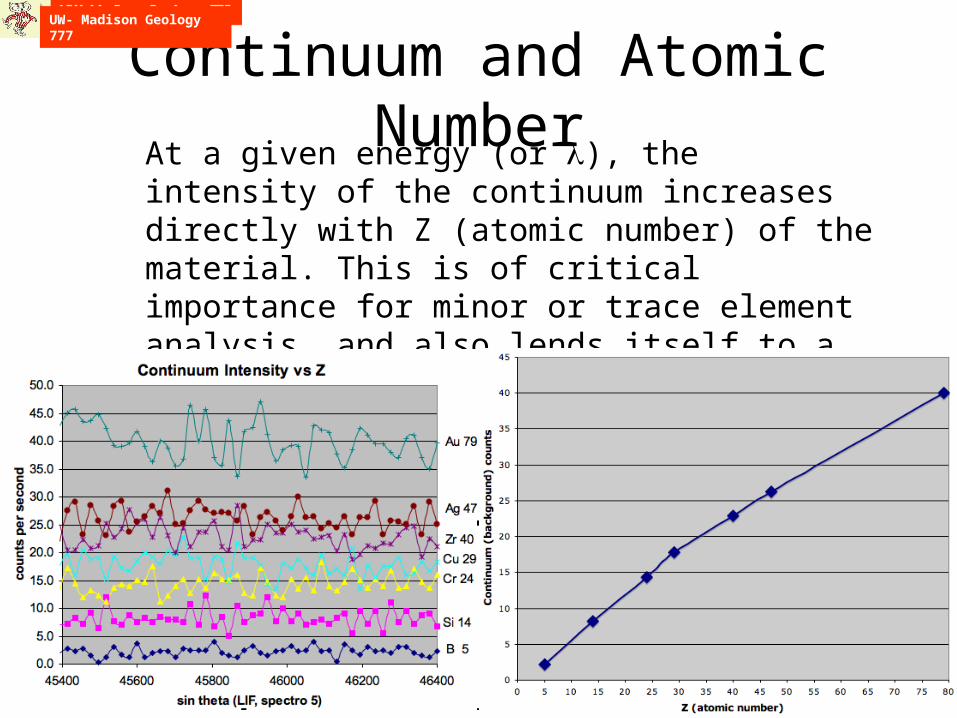
Continuum and Atomic NumberAt a given energy (or ), the
intensity of the continuum increases directly with Z (atomic number) of the material. This is of critical importance for minor or trace element analysis, and also lends itself to a timesaving technique (Mean Atomic Number,“MAN”).
UW- Madison Geology 777
However…
“X-ray mapping” of predefined elements is now pretty much a thing of the past (or of EDS systems purchased before 2000 or so).
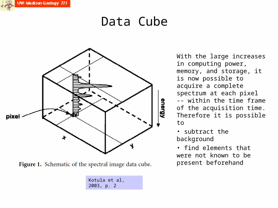
Data Cube
With the large increases in computing power, memory, and storage, it is now possible to acquire a complete spectrum at each pixel -- within the time frame of the acquisition time.Therefore it is possible to• subtract the background • find elements that were not known to be present beforehand
Kotula et al, 2003, p. 2

Spectral (“hyperspectral”)
ImagingHere any and all x-rays detected are mapped to each pixel over which the beam is scanning. This is both very powerful (see elements not known to be present before starting), but also loses something relative to other ‘slower old-fashioned’ maps--lower counts in peak channels.
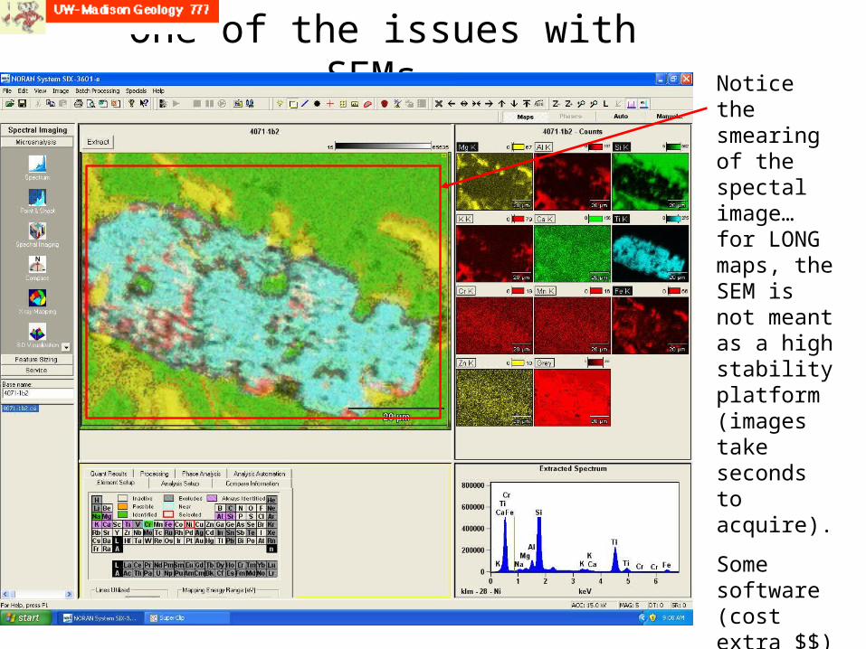
One of the issues with SEMs… Notice
the smearing of the spectal image… for LONG maps, the SEM is not meant as a high stability platform (images take seconds to acquire).
Some software (cost extra $$) use a reference point for each frame and if there is drift, correct for it.

Multivariate statistical analysis
Paul Kotula et al demonstrated the usefulness of applying “principal component analysis” to spectra images.
They developed a procedure for converting from abstract principal components to physically meaningful pure components.
Kotula et al, 2003, p. 3
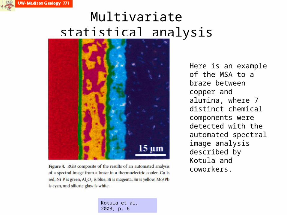
Multivariate statistical analysis
Here is an example of the MSA to a braze between copper and alumina, where 7 distinct chemical components were detected with the automated spectral image analysis described by Kotula and coworkers.
Kotula et al, 2003, p. 6
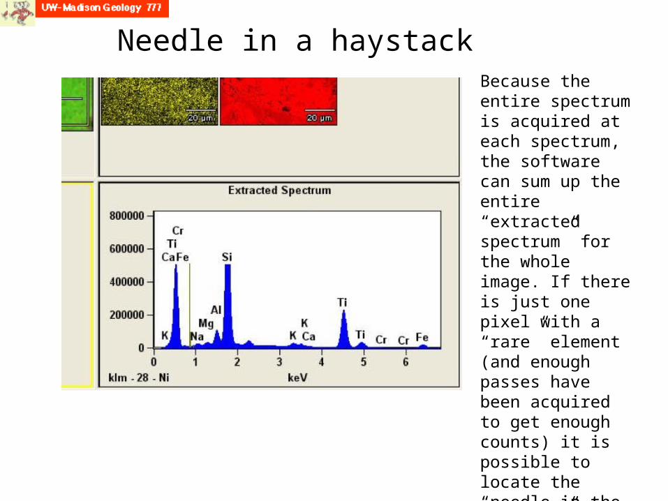
Needle in a haystackBecause the entire spectrum is acquired at each spectrum, the software can sum up the entire “extracted spectrum” for the whole image. If there is just one pixel with a “rare” element (and enough passes have been acquired to get enough counts) it is possible to locate the “needle in the haystack” using these spectrum images.
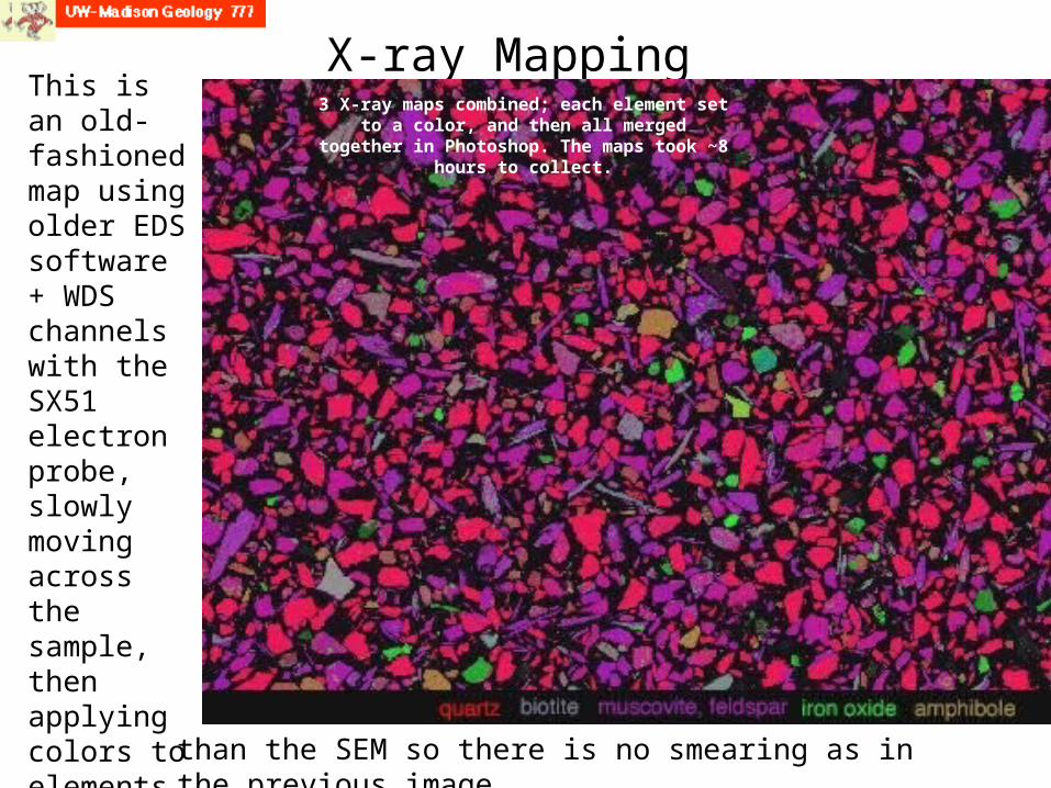
X-ray Mapping3 X-ray maps combined; each element set
to a color, and then all merged together in Photoshop. The maps took ~8
hours to collect.
This is an old-fashioned map using older EDS software + WDS channels with the SX51 electron probe, slowly moving across the sample, then applying colors to elements. This instrument is built to be more stable
than the SEM so there is no smearing as in the previous image.

Feature Sizing, Chemical Typing
This is a valuable feature of the SEM for locating and identifying a particular mineral in a mixed population (e.g. K-rich minerals mixed with K-poor minerals.
1. Acquire BSE image with good contrast so the K-rich mineral is distinct
2. Set a desired brightness level as the test for the mineral in question (if brighter than, then acquire short EDS spectrum of center of grain)
3. Set elements to be evaluated; set short (~2 second) EDS acquisition time
4. Set the stage coordinates of the corners of the area; Run the program
5. Return the next day and look at the list of grains it acquired EDS spectra; order from high to low K; then drive to each grain to verify it is the grain you want.
The next 3 slides go through the process…
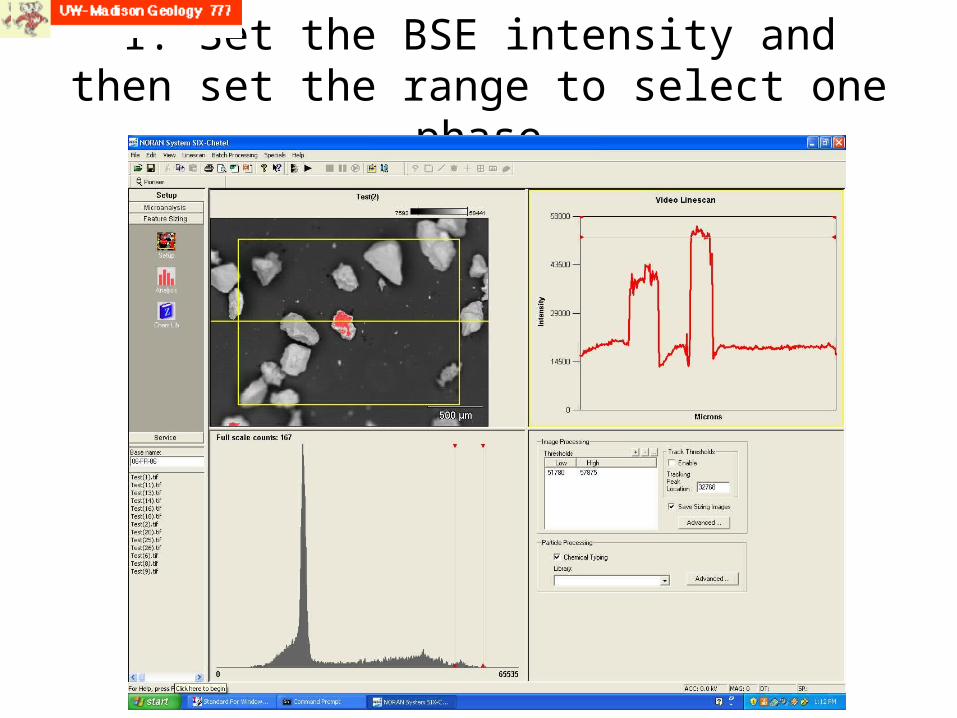
1. Set the BSE intensity and then set the range to select one
phase

2. Select the elements needed to find the phase
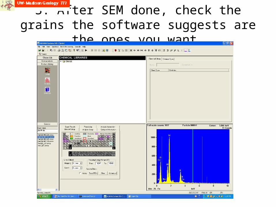
3. After SEM done, check the grains the software suggests are
the ones you want

“What will they think of next?”
The veritable scanning electron microscope keeps providing more and more opportunities for improvement and innovation…
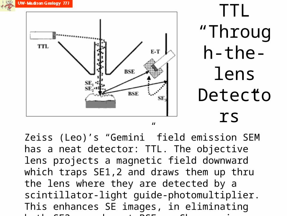
TTL“Through-the-lens
Detectors”
Zeiss (Leo)’s “Gemini” field emission SEM has a neat detector: TTL. The objective lens projects a magnetic field downward which traps SE1,2 and draws them up thru the lens where they are detected by a scintillator-light guide-photomultiplier. This enhances SE images, in eliminating both SE3s and most BSEs. …Sharper images…

Energy filtering of SEs
At the August 2010 Microscopy and Microanalysis meeting in Portland OR, I found one talk to be very interesting:
Someone working with FEI, and operating a low E0s, has found a way to “energy filter” the very low energy secondary electrons, producing a technique to “see through” the common surface contamination on materials. The slightly higher energy SEs (say 10 eV) result from the impact of the E0 electrons with the surface contamination layer, whereas those SEs coming from the material under the contamination have lower energy (say 2 eV).
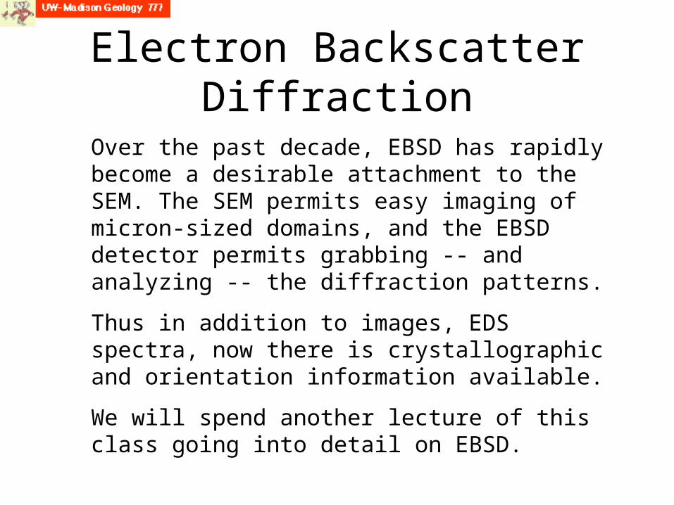
Electron Backscatter Diffraction
Over the past decade, EBSD has rapidly become a desirable attachment to the SEM. The SEM permits easy imaging of micron-sized domains, and the EBSD detector permits grabbing -- and analyzing -- the diffraction patterns.
Thus in addition to images, EDS spectra, now there is crystallographic and orientation information available.
We will spend another lecture of this class going into detail on EBSD.
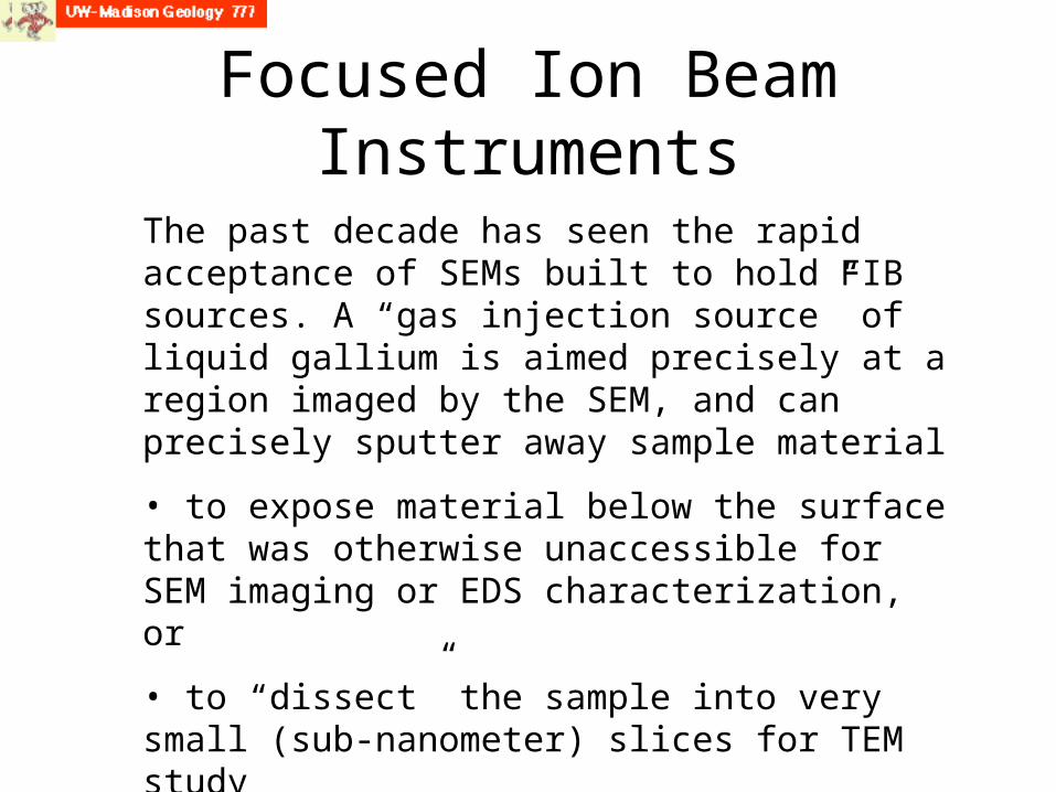
Focused Ion Beam Instruments
The past decade has seen the rapid acceptance of SEMs built to hold FIB sources. A “gas injection source” of liquid gallium is aimed precisely at a region imaged by the SEM, and can precisely sputter away sample material
• to expose material below the surface that was otherwise unaccessible for SEM imaging or EDS characterization, or
• to “dissect” the sample into very small (sub-nanometer) slices for TEM study

Focused Ion Beam Instruments
From JAMES D. SCHIFFBAUER and SHUHAI XIAO, 2009
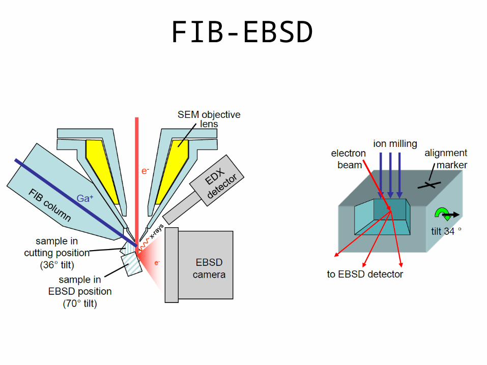
FIB-EBSD
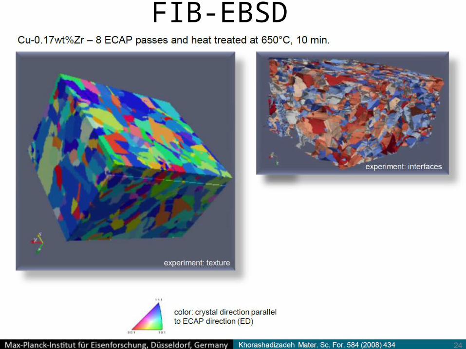
FIB-EBSD
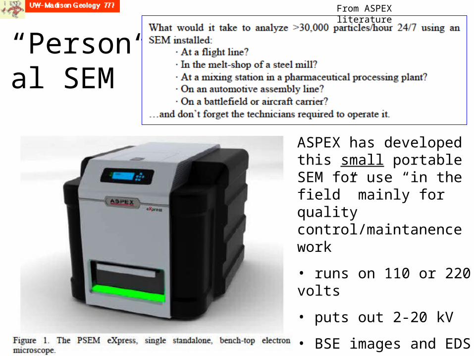
“Personal SEM”
ASPEX has developed this small portable SEM for use “in the field” mainly for quality control/maintanence work
• runs on 110 or 220 volts
• puts out 2-20 kV
• BSE images and EDS
• portable, easily fits in the back of a van or SUV
From ASPEX literature