Selective laser melted TiB2/Ti6Al4V graded materials and first...
4
Selective laser melted TiB 2 /Ti6Al4V graded materials and first-principle calculations Rui Wang a,b , Dongdong Gu a,b,⇑ , Lixia Xi a,b , Kaijie Lin a,b , Meng Guo a,b , Hongmei Zhang a,b a College of Materials Science and Technology, Nanjing University of Aeronautics and Astronautics, Yudao Street 29, Nanjing 210016, Jiangsu Province, PR China b Jiangsu Provincial Engineering Laboratory for Laser Additive Manufacturing of High-Performance Metallic Components, Nanjing University of Aeronautics and Astronautics, Yudao Street 29, Nanjing 210016, Jiangsu Province, PR China article info Article history: Received 14 May 2019 Received in revised form 23 June 2019 Accepted 4 July 2019 Available online 5 July 2019 Keywords: Selective laser melting Interfaces Microstructure Graded materials First-principle calculations abstract Selective laser melting (SLM), as a rapidly developed layer-by-layer 3D printing technology, has been demonstrated that it can be used for additive manufacturing of multi-materials. In this work, TiB 2 / Ti6Al4V multi-materials were manufactured by SLM. The results showed that interfacial microstructures consisting of un-melted TiB 2 powders, columnar TiB crystals, and acicular TiB crystals were formed in the molten pool. Meanwhile, a variation nanohardness was developed with chemical compositions at the interfacial regions, owing to an in-situ reaction of Ti and TiB 2 . The first-principle calculations were used to reveal the axial growth of TiB crystals as well as the different hardness of this system. Ó 2019 Published by Elsevier B.V. 1. Introduction Selective laser melting (SLM), as a rapidly developed layer by layer additive manufacturing technique, is capable to produce high densification and complex parts by using of metal, ceramic, or composite materials [1,2]. For many practical engineering applica- tions, multi-materials SLM is indispensable due to the requirement of different material properties at different regions. Tan et al. have clearly revealed the feasibility of combining different metals with good metallurgical bonding using SLM [3]. Compared with metal- metal multiple materials, there are more challenges for SLM of metal-ceramic multiple materials. These are involved with the extremely different bond strength and thermal expansion coefficient between metal and ceramic, leading to thermal stress and even delamination during non-equilibrium solidification of SLM [4]. To overcome the above constraints, fabrication of functional graded materials (FGM) through good interfacial bonding between metal and ceramic is feasible. This method can avoid residual stress concentration and fracture propagation by reducing the saltation of different properties between neighboring layers [5,6]. Shishkovsky et al. [7] have successfully fabricated functional graded specimens and realized a hardness gradient via SLM using the compositionally grade powders (Ti+(10, 15 or 20 vol.%) TiB 2 ). The nanohardness of SLMed Ti6Al4V with 3 wt% TiB 2 can reach to 6.00 GPa due to the reinforcement effect of needle-like TiB [8]. Nevertheless, it is difficult to make a larger range of hardness dif- ference for multi-materials SLM of pure TiB 2 and Ti6Al4V powders instead of composite powders. Interfacial reaction and microstruc- ture are vital to the connection characteristic of adjacent layers. In this work, graded materials were prepared by SLM of TiB 2 /Ti6Al4V multi-materials. The microstructure and nanohardness at the interface were investigated. Additionally, first-principle calcula- tions were used to explain the axial growth of TiB and different hardness of this system. 2. Materials and methods The SLM equipment was composed of an IPG YLR-500 Ytter- bium fiber laser with a 1070 ± 10 nm wavelength. Fig. 1a shows the SLM process of Ti6Al4V and TiB 2 powders. Cubic samples were fabricated layer by layer on a Ti6Al4V substrate. Based on our pre- vious research [9], the laser power (P), scanning speed (v) and hatch spacing of Ti6Al4V layer were 250 W, 600 mm/s, and 50 lm, respectively. While for the TiB 2 layer, the respective laser scanning speed and hatch spacing were set as 80 mm/s and 120 lm. The laser power varied from 200 W to 500 W with an interval of 50 W. The starting powders of Ti6Al4V (99.7% purity, https://doi.org/10.1016/j.matlet.2019.07.015 0167-577X/Ó 2019 Published by Elsevier B.V. ⇑ Corresponding author at: College of Materials Science and Technology, Nanjing University of Aeronautics and Astronautics, Yudao Street 29, Nanjing 210016, Jiangsu Province, PR China. E-mail address: [email protected] (D. Gu). Materials Letters 254 (2019) 33–36 Contents lists available at ScienceDirect Materials Letters journal homepage: www.elsevier.com/locate/mlblue
Transcript of Selective laser melted TiB2/Ti6Al4V graded materials and first...
Materials Letters 254 (2019) 33–36
Contents lists available at ScienceDirect
Materials Letters
journal homepage: www.elsevier .com/locate /mlblue
Selective laser melted TiB2/Ti6Al4V graded materials and first-principlecalculations
https://doi.org/10.1016/j.matlet.2019.07.0150167-577X/� 2019 Published by Elsevier B.V.
⇑ Corresponding author at: College of Materials Science and Technology, NanjingUniversity of Aeronautics and Astronautics, Yudao Street 29, Nanjing 210016,Jiangsu Province, PR China.
E-mail address: [email protected] (D. Gu).
Rui Wang a,b, Dongdong Gu a,b,⇑, Lixia Xi a,b, Kaijie Lin a,b, Meng Guo a,b, Hongmei Zhang a,b
aCollege of Materials Science and Technology, Nanjing University of Aeronautics and Astronautics, Yudao Street 29, Nanjing 210016, Jiangsu Province, PR Chinab Jiangsu Provincial Engineering Laboratory for Laser Additive Manufacturing of High-Performance Metallic Components, Nanjing University of Aeronautics and Astronautics,Yudao Street 29, Nanjing 210016, Jiangsu Province, PR China
a r t i c l e i n f o
Article history:Received 14 May 2019Received in revised form 23 June 2019Accepted 4 July 2019Available online 5 July 2019
Keywords:Selective laser meltingInterfacesMicrostructureGraded materialsFirst-principle calculations
a b s t r a c t
Selective laser melting (SLM), as a rapidly developed layer-by-layer 3D printing technology, has beendemonstrated that it can be used for additive manufacturing of multi-materials. In this work, TiB2/Ti6Al4V multi-materials were manufactured by SLM. The results showed that interfacial microstructuresconsisting of un-melted TiB2 powders, columnar TiB crystals, and acicular TiB crystals were formed in themolten pool. Meanwhile, a variation nanohardness was developed with chemical compositions at theinterfacial regions, owing to an in-situ reaction of Ti and TiB2. The first-principle calculations were usedto reveal the axial growth of TiB crystals as well as the different hardness of this system.
� 2019 Published by Elsevier B.V.
1. Introduction
Selective laser melting (SLM), as a rapidly developed layer bylayer additive manufacturing technique, is capable to produce highdensification and complex parts by using of metal, ceramic, orcomposite materials [1,2]. For many practical engineering applica-tions, multi-materials SLM is indispensable due to the requirementof different material properties at different regions. Tan et al. haveclearly revealed the feasibility of combining different metals withgood metallurgical bonding using SLM [3]. Compared with metal-metal multiple materials, there are more challenges for SLM ofmetal-ceramic multiple materials. These are involved with theextremely different bond strength and thermal expansioncoefficient between metal and ceramic, leading to thermal stressand even delamination during non-equilibrium solidification ofSLM [4].
To overcome the above constraints, fabrication of functionalgraded materials (FGM) through good interfacial bonding betweenmetal and ceramic is feasible. This method can avoid residualstress concentration and fracture propagation by reducing thesaltation of different properties between neighboring layers [5,6].Shishkovsky et al. [7] have successfully fabricated functional
graded specimens and realized a hardness gradient via SLM usingthe compositionally grade powders (Ti+(10, 15 or 20 vol.%) TiB2).The nanohardness of SLMed Ti6Al4V with 3 wt% TiB2 can reachto 6.00 GPa due to the reinforcement effect of needle-like TiB [8].Nevertheless, it is difficult to make a larger range of hardness dif-ference for multi-materials SLM of pure TiB2 and Ti6Al4V powdersinstead of composite powders. Interfacial reaction and microstruc-ture are vital to the connection characteristic of adjacent layers. Inthis work, graded materials were prepared by SLM of TiB2/Ti6Al4Vmulti-materials. The microstructure and nanohardness at theinterface were investigated. Additionally, first-principle calcula-tions were used to explain the axial growth of TiB and differenthardness of this system.
2. Materials and methods
The SLM equipment was composed of an IPG YLR-500 Ytter-bium fiber laser with a 1070 ± 10 nm wavelength. Fig. 1a showsthe SLM process of Ti6Al4V and TiB2 powders. Cubic samples werefabricated layer by layer on a Ti6Al4V substrate. Based on our pre-vious research [9], the laser power (P), scanning speed (v) andhatch spacing of Ti6Al4V layer were 250 W, 600 mm/s, and50 lm, respectively. While for the TiB2 layer, the respective laserscanning speed and hatch spacing were set as 80 mm/s and120 lm. The laser power varied from 200 W to 500W with aninterval of 50 W. The starting powders of Ti6Al4V (99.7% purity,
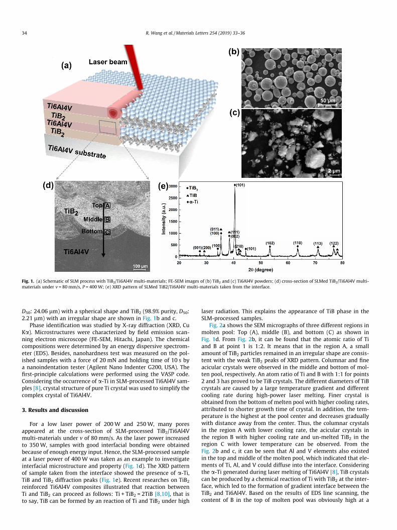
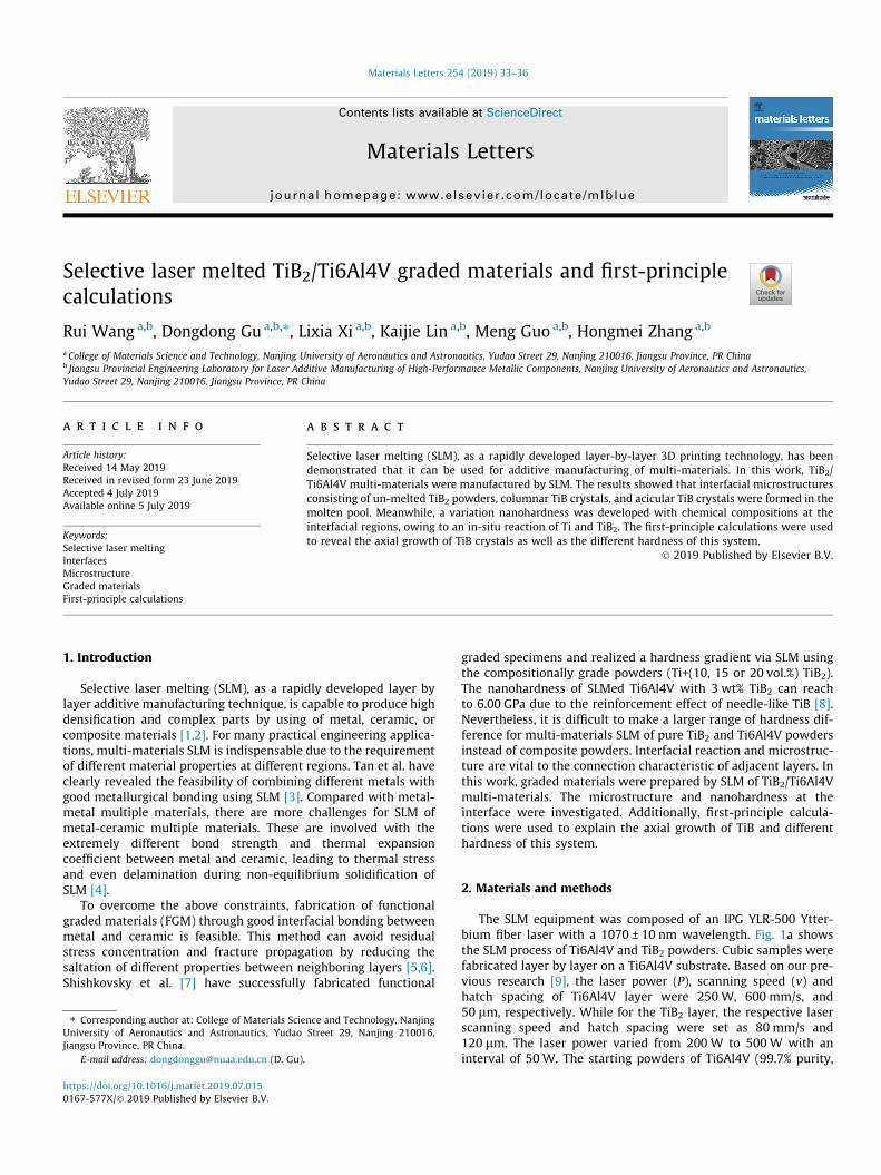
Fig. 1. (a) Schematic of SLM process with TiB2/Ti6Al4V multi-materials; FE-SEM images of (b) TiB2 and (c) Ti6Al4V powders; (d) cross-section of SLMed TiB2/Ti6Al4V multi-materials under v = 80 mm/s, P = 400W; (e) XRD pattern of SLMed TiB2/Ti6Al4V multi-materials taken from the interface.
34 R. Wang et al. /Materials Letters 254 (2019) 33–36
D50: 24.06 lm) with a spherical shape and TiB2 (98.9% purity, D50:2.21 lm) with an irregular shape are shown in Fig. 1b and c.
Phase identification was studied by X-ray diffraction (XRD, CuKa). Microstructures were characterized by field emission scan-ning electron microscope (FE-SEM, Hitachi, Japan). The chemicalcompositions were determined by an energy dispersive spectrom-eter (EDS). Besides, nanohardness test was measured on the pol-ished samples with a force of 20 mN and holding time of 10 s bya nanoindentation tester (Agilent Nano Indenter G200, USA). Thefirst-principle calculations were performed using the VASP code.Considering the occurrence of a-Ti in SLM-processed Ti6Al4V sam-ples [8], crystal structure of pure Ti crystal was used to simplify thecomplex crystal of Ti6Al4V.
3. Results and discussion
For a low laser power of 200 W and 250W, many poresappeared at the cross-section of SLM-processed TiB2/Ti6Al4Vmulti-materials under v of 80 mm/s. As the laser power increasedto 350 W, samples with good interfacial bonding were obtainedbecause of enough energy input. Hence, the SLM-processed sampleat a laser power of 400 W was taken as an example to investigateinterfacial microstructure and property (Fig. 1d). The XRD patternof sample taken from the interface showed the presence of a-Ti,TiB and TiB2 diffraction peaks (Fig. 1e). Recent researches on TiB2
reinforced Ti6Al4V composites illustrated that reaction betweenTi and TiB2 can proceed as follows: Ti + TiB2 = 2TiB [8,10], that isto say, TiB can be formed by an reaction of Ti and TiB2 under high
laser radiation. This explains the appearance of TiB phase in theSLM-processed samples.
Fig. 2a shows the SEM micrographs of three different regions inmolten pool: Top (A), middle (B), and bottom (C) as shown inFig. 1d. From Fig. 2b, it can be found that the atomic ratio of Tiand B at point 1 is 1:2. It means that in the region A, a smallamount of TiB2 particles remained in an irregular shape are consis-tent with the weak TiB2 peaks of XRD pattern. Columnar and fineacicular crystals were observed in the middle and bottom of mol-ten pool, respectively. An atom ratio of Ti and B with 1:1 for points2 and 3 has proved to be TiB crystals. The different diameters of TiBcrystals are caused by a large temperature gradient and differentcooling rate during high-power laser melting. Finer crystal isobtained from the bottom of melten pool with higher cooling rates,attributed to shorter growth time of crystal. In addition, the tem-perature is the highest at the pool center and decreases graduallywith distance away from the center. Thus, the columnar crystalsin the region A with lower cooling rate, the acicular crystals inthe region B with higher cooling rate and un-melted TiB2 in theregion C with lower temperature can be observed. From theFig. 2b and c, it can be seen that Al and V elements also existedin the top and middle of the molten pool, which indicated that ele-ments of Ti, Al, and V could diffuse into the interface. Consideringthe a-Ti generated during laser melting of Ti6Al4V [8], TiB crystalscan be produced by a chemical reaction of Ti with TiB2 at the inter-face, which led to the formation of gradient interface between theTiB2 and Ti6Al4V. Based on the results of EDS line scanning, thecontent of B in the top of molten pool was obviously high at a

Fig. 2. (a) FE-SEMmicrographs showing the different regions of A, B and C of the molten pool in Fig. 1d; (b) chemical compositions by EDS analysis: atomic fraction of Ti, B, Aland V elements at three different positions in Fig. 2a; (c) EDS line-scan analysis and (d) nanoindentation along the line in Fig. 1d.
R. Wang et al. /Materials Letters 254 (2019) 33–36 35
depth of 0–30 lm and its content gradually stabilized at about 30–240 lm, then started to decline. This suggests that boron diffusionis hard to traverse the pool boundary into Ti6Al4V. However, theincreasing intensity of Ti, Al, V at a depth of 250 lm indicate thereaching of Ti6Al4V layer. In general, the TiB crystals in the transi-tion region alleviate the residual stress due to gradientcompositions.
Nanohardness measurements were conducted on the interfacialregion of TiB2/Ti6Al4V and the results are shown in Fig. 2d.Nanohardness with an approximate value of 4.8 GPa for Ti6Al4Vlayer is comparable to reported values [11,12]. According to thegradient change of nanohardness across the interfacial region, itis noted that TiB makes a good transition between the TiB2 andTi alloy. Therefore, TiB2/TiB/Ti6Al4V graded materials promotethe formation of good bonding between dissimilar materials. Thisgraded materials additive manufacturing is beneficial to combinethe hard ceramic with ductile metal into an organic wholeeffectively.
The theoretical calculations were performed to investigate thephysical origins of different hardness between TiB2, TiB, andTi6Al4V. Fig. 3a shows that a-Ti are composed of metallic bond(dTi-Ti = 2.86 Å). From the supercell, both TiB and TiB2 are mainlyconsisted of B-B covalent bonds, and the covalent bond length of
TiB (dB-B = 1.81 Å) is larger than TiB2 (dB-B = 1.75 Å). Therefore, thecovalency of TiB is weaker than that of TiB2. As the hardness of amaterial is a reflection of the internal bonding strength, and theimpacts of several chemical bonds are covalent bond > ionicbond > metal bond. Thus, the hardness order of these three materi-als is TiB2 > TiB > Ti (Ti6Al4V). Apart from the crystal structure cal-culation, the electronic structure has been also studied. The chargedistributions of TiB and TiB2 are shown in Fig. 3b, zigzag chain ofTiB and hexagonal network structure of TiB2 demonstrate the delo-calized p-bonds between the boron atoms. In this situation, TiBstructure characterized by zigzag chains of boron atoms is parallelto the [0 1 0] direction, this anisotropic crystal structure may beresponsible for an axial growth as observed in Fig. 2a. FromFig. 3c, it can be seen that a-Ti exhibits a good metallicity due tolocal electronic density of states around the fermi level. The elec-tronic structures of both TiB and TiB2 are governed by the stronghybridization between the Ti-3d and B-2p states. In particular,the appearance of the pseudo-gap (yellow region) around the fermilevel also lead to increased stability of TiB2. Therefore, the struc-ture stability is in an order of TiB2 > TiB > Ti6Al4V. Hardness andelasticity of these materials with distinct bonding may show a sim-ilar gradient tendency, which contributes to less residual stressand good interfacial bonding.

Fig. 3. (a) Unit cell and supercell of Ti, TiB and TiB2; (b) charge distribution of TiB and TiB2; (c) partial density of states of the system.
36 R. Wang et al. /Materials Letters 254 (2019) 33–36
4. Conclusions
TiB2/TiB/Ti6Al4V graded materials have been achieved by SLMof TiB2/Ti6Al4V multi-materials. TiB was formed by an in-situreaction of Ti with TiB2 and the gradual variations of chemicalcompositions caused a variation in nanohardness along theinterface. The structural stabilities of TiB2, TiB, and Ti6Al4V werealso studied by first-principle calculations. The hardness gradientof TiB2 > TiB > Ti6Al4V was demonstrated by our theoretical andexperimental investigations. These findings demonstrate thatgraded materials additive manufacturing is beneficial to fabricatemetal-ceramic part successfully.
Declaration of Competing Interest
The authors have declared that no conflict of interest exists.
Acknowledgements
This work was supported by the National Natural Science Foun-dation of China (No. 51735005), and the National Key Research andDevelopment Program (No. 2016YFB1100101).
References
[1] C.Y. Yap, C.K. Chua, Z.L. Dong, Z.H. Liu, D.Q. Zhang, L.E. Loh, S.L. Sing, Appl. Phys.Rev. 2 (2015) 041101.
[2] H. Chen, D. Gu, D. Dai, M. Xia, C. Ma, Mater. Lett. 227 (2018) 128–131.[3] C. Tan, K. Zhou, T. Kuang, Mater. Lett. 237 (2019) 328–331.[4] J. Koopmann, J. Voigt, T. Niendorf, Metall. Mater. Trans. B. 50 (2019) 1042–
1051.[5] M. Kashtalyan, M. Menshykova, Compos. Struct. 87 (2009) 36–43.[6] H. Chai, B. Lawn, J. Mater. Res. 15 (2000) 1017–1024.[7] I. Shishkovsky, N. Kakovkina, V. Sherbakov, Compos. Struct. 169 (2017) 90–96.[8] C. Cai, C. Radoslaw, J. Zhang, Q. Yan, S. Wen, B. Song, Y. Shi, Powder Technol.
342 (2019) 73–84.[9] D. Sun, D. Gu, K. Lin, J. Ma, W. Chen, J. Huang, X. Sun, M. Chu, Powder Technol.
342 (2019) 371–379.[10] H. Attar, M. Bönisch, M. Calin, L. Zhang, S. Scudino, J. Eckert, Acta Mater. 76
(2014) 13–22.[11] L.Y. Chen, J.C. Huang, C.H. Lin, S.Y. Chen, T.L. Yang, D.Y. Lin, H.K. Lin, J.S.C. Jang,
Mater. Sci. Eng. A. 682 (2017) 389–395.[12] W. Xue, C. Wang, R. Chen, Z. Deng, Mater. Lett. 52 (2002) 435–441.