Selecting advanced MOSFETs for automotive power design
9
Selecting advanced MOSFETs for automotive power design
Transcript of Selecting advanced MOSFETs for automotive power design
Selecting advanced MOSFETs for automotive power design
Whitepaper
Copyright 2019 © TOSHIBA ELECTRONICS EUROPE GMBH, All Rights Reserved.
Selecting advanced MOSFETs for automotive power design
From powertrains to safety systems and from comfort features to vehicle lights, MOSFETs play an important role in the modern automobile. As the electronic content of vehicles continues to grow, and as e-mobility becomes popular, these devices are becoming increasingly important. Irrespective of the target application, today’s automotive MOSFETs have a vital role to play in reducing system losses - delivering better fuel economy and reduced emissions in conventional vehicles and offering longer travel distance between charges in the case of EVs and HEVs. At the same time, these MOSFETs must realize the higher power densities and better thermal performance that help designers save board space and reduce component count. In this whitepaper we look at the evolution of DPAK and D2PAK class automotive power MOSFETs and show how the latest advances in packaging and processes are addressing today’s demanding automotive applications.
Introduction MOSFET requirements vary depending on what the device is being used for, and where it is placed in the vehicle. Manufacturers address this wide range of needs by developing broad product portfolios that offer multiple options in terms of performance and package type. These MOSFETs need to be qualified to automotive standards such as AEC-Q101. As the demand for electronic applications grows, then the number of power devices deployed in a vehicle also rises. Voltages are increasing from 12V through 24V to 48V for the battery string. This means that the demand of 100V MOSFETs are increased. Finally, in the increasingly dense spaces within modern vehicles, ambient temperatures are higher than in consumer, computing or even industrial applications. This brings a significant challenge to system designers as there is less margin for temperature rise in the device.
Addressing the challenges Semiconductor companies have two main thrusts in addressing these challenges; electrical and thermal. From an electrical perspective, the semiconductor performances are constantly improved, along with the associated wafer technology to reduce resistances and capacitances in the final device. These improvements bring greater efficiencies and allow for faster switching, delivering MOSFETs suitable for today’s high-power-density applications. In parallel with this, development effort is being focused on the package technology. Smaller packages have to be used to realize the downsizing of ECU(Electronic Control Unit). The challenge is how to realize the same level of thermal conductivity in smaller spaces. As a result, companies are developing innovative ways to thermally connect the semiconductor junction to the outside world, enabling the greater thermal efficiencies demanded in compact high-power systems that operate at elevated ambient temperatures. As a company that has been developing automotive power MOSFETs for many years, Toshiba is at the forefront of innovation for today’s demanding vehicle applications. The company’s portfolio of automotive power MOSFETs encompasses N-channel and P-channel devices (the latter are particularly useful for reverse battery protection) based on trench gate technology. Toshiba’s trench processes offer the best combination of conduction and switching performance in the target voltage range.
Whitepaper
Copyright 2019 © TOSHIBA ELECTRONICS EUROPE GMBH, All Rights Reserved.
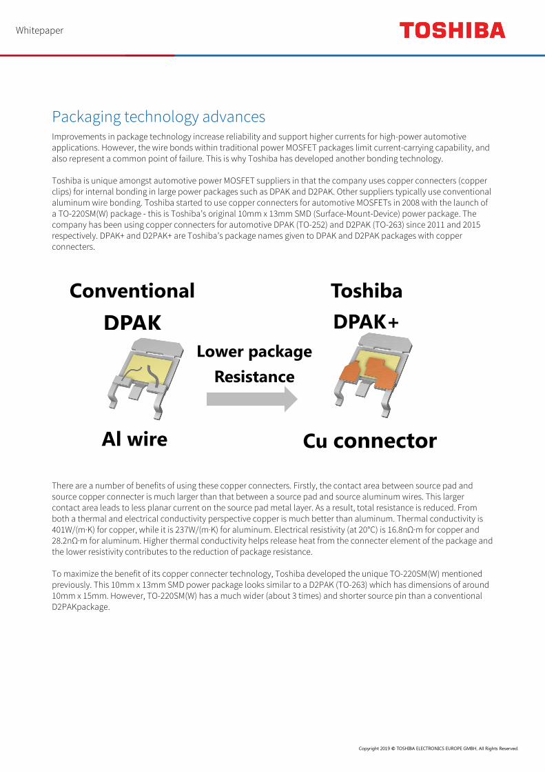
Packaging technology advances Improvements in package technology increase reliability and support higher currents for high-power automotive applications. However, the wire bonds within traditional power MOSFET packages limit current-carrying capability, and also represent a common point of failure. This is why Toshiba has developed another bonding technology. Toshiba is unique amongst automotive power MOSFET suppliers in that the company uses copper connecters (copper clips) for internal bonding in large power packages such as DPAK and D2PAK. Other suppliers typically use conventional aluminum wire bonding. Toshiba started to use copper connecters for automotive MOSFETs in 2008 with the launch of a TO-220SM(W) package - this is Toshiba’s original 10mm x 13mm SMD (Surface-Mount-Device) power package. The company has been using copper connecters for automotive DPAK (TO-252) and D2PAK (TO-263) since 2011 and 2015 respectively. DPAK+ and D2PAK+ are Toshiba’s package names given to DPAK and D2PAK packages with copper connecters.
There are a number of benefits of using these copper connecters. Firstly, the contact area between source pad and source copper connecter is much larger than that between a source pad and source aluminum wires. This larger contact area leads to less planar current on the source pad metal layer. As a result, total resistance is reduced. From both a thermal and electrical conductivity perspective copper is much better than aluminum. Thermal conductivity is 401W/(m·K) for copper, while it is 237W/(m·K) for aluminum. Electrical resistivity (at 20°C) is 16.8nΩ·m for copper and 28.2nΩ·m for aluminum. Higher thermal conductivity helps release heat from the connecter element of the package and the lower resistivity contributes to the reduction of package resistance. To maximize the benefit of its copper connecter technology, Toshiba developed the unique TO-220SM(W) mentioned previously. This 10mm x 13mm SMD power package looks similar to a D2PAK (TO-263) which has dimensions of around 10mm x 15mm. However, TO-220SM(W) has a much wider (about 3 times) and shorter source pin than a conventional D2PAKpackage.
Conventional DPAK
Al wire
Toshiba DPAK+
Cu connector
Lower package Resistance

Whitepaper
Copyright 2019 © TOSHIBA ELECTRONICS EUROPE GMBH, All Rights Reserved.
TO-2 2 0 SM (W) PACKAGE (10mm x 13mm)
D2PAK(TO-263) TO-220SM(W)
Whitepaper
Copyright 2019 © TOSHIBA ELECTRONICS EUROPE GMBH, All Rights Reserved.
MOSFET on-resistance comparisons
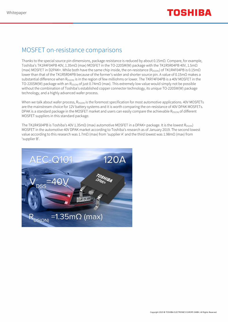
Thanks to the special source pin dimensions, package resistance is reduced by about 0.15mΩ. Compare, for example, Toshiba’s TK1R4F04PB 40V, 1.35mΩ (max) MOSFET in the TO-220SM(W) package with the TK1R5R04PB 40V, 1.5mΩ (max) MOSFET in D2PAK+. While both have the same chip inside, the on-resistance (RDS(ON)) of TK1R4F04PB is 0.15mΩ lower than that of the TK1R5R04PB because of the former’s wider and shorter source pin. A value of 0.15mΩ makes a substantial difference when RDS(ON) is in the region of few milliohms or lower. The TKR74F04PB is a 40V MOSFET in the TO-220SM(W) package with an RDS(ON) of just 0.74mΩ (max). This extremely low value would simply not be possible without the combination of Toshiba’s established copper connecter technology, its unique TO-220SW(W) package technology, and a highly advanced wafer process. When we talk about wafer process, RDS(ON) is the foremost specification for most automotive applications. 40V MOSFETs are the mainstream choice for 12V battery systems and it is worth comparing the on-resistance of 40V DPAK MOSFETs. DPAK is a standard package in the MOSFET market and users can easily compare the achievable RDS(ON) of different MOSFET suppliers in this standard package. The TK1R4S04PB is Toshiba’s 40V 1.35mΩ (max) automotive MOSFET in a DPAK+ package. It is the lowest RDS(ON) MOSFET in the automotive 40V DPAK market according to Toshiba’s research as of January 2019. The second lowest value according to this research was 1.7mΩ (max) from ‘supplier A’ and the third lowest was 1.98mΩ (max) from ‘supplier B’.

Whitepaper
Copyright 2019 © TOSHIBA ELECTRONICS EUROPE GMBH, All Rights Reserved.
DPAK+ PACKAGE (6.5mm x 9.5mm)
Considering the expected growth in 48V battery systems, 100V MOSFETs become increasingly important. Once again we can compare the on-resistance specifications of DPAK devices at this voltage. For example, the TK55S10N1 is a 100V 6.5mΩ (max) MOSFET in the DPAK+ package from Toshiba. This is the lowest RDS(ON) value for 100V DPAK automotive MOSFET according to Toshiba’s research as of December 2016. The second lowest rating was 6.6mΩ (max) from ‘supplier B’ and the third lowest rating was 8mΩ (max) from ‘supplier C’. It is worth noting that Toshiba is going to release a 100V 6.1mΩ (max) MOSFET in a DPAK+ package in 2017.

Whitepaper
Copyright 2019 © TOSHIBA ELECTRONICS EUROPE GMBH, All Rights Reserved.
Conclusion For motors employed in a 48V battery system, the target motor power range is typically around 1~10kW. In order to drive a 5kW motor – for instance of a type employed for a BSG (Belt Starter Generator) - in such a scheme MOSFETs have to be connected in parallel to drive high current and dissipate high power. Parallel connection of MOSFETs is not something new, but it does require careful design. In particular, it is important to pay attention to the switching timing difference among paralleled MOSFETs. This is because the more difference there is in switching timing the more imbalance of switching loss there is likely to be among the paralleled devices. If one MOSFET turns on earlier or turns off later than the other MOSFETs in the parallel set-up, the switching loss concentrates around this single MOSFET. To address this issue, Toshiba released its TK160F10N1L - a new 100V, 160A power MOSFET that provides a tighter threshold voltage (Vth) specification than previous devices. Offering Vth specs of min2.5V/max3.5V versus its predecessor’s min2V/max4V, the TK160F10N1L is ideal for automotive power switching applications. Thanks to this tighter Vth spec, switching loss is distributed more evenly among the MOSFETs.
When it comes to switching, there is another important characteristic as illustrated in the figure below. Here we see two waveforms of Toshiba MOSFETs during switch-off. The figure shows that the ringing time of the TK100S04N1L, which is based on Toshiba’s UMOS8 semiconductor process, is reduced to half of that of the TK80S04K3L, which is based on an older UMOS4 process. The result is that noise emission is greatly reduced thanks to the improved dynamic characteristics of UMOS8.
Whitepaper
Copyright 2019 © TOSHIBA ELECTRONICS EUROPE GMBH, All Rights Reserved.
Finally, it is worth noting that Toshiba has a comprehensive product portfolio of P-channel MOSFETs, which are often used for reverse battery protection or as the high-side switch of Half-/H-/B6-bridge circuits. Because no charge pump is needed to drive a P-channel MOSFET, the gate drive circuit can be very simple and cost-effective. Furthermore, the lack of a constantly switching charge pump, which gate drivers for N-channel MOSFETs usually have, can also contribute to reduced noise emissions.

Whitepaper
Copyright 2019 © TOSHIBA ELECTRONICS EUROPE GMBH, All Rights Reserved.
Restrictions On Product Use
Toshiba Corporation and its subsidiaries and affiliates are collectively referred to as “TOSHIBA”. Hardware, software and systems described in this document are collectively referred to as “Product”. • TOSHIBA reserves the right to make changes to the information in this document and related Product without notice. • This document and any information herein may not be reproduced without prior written permission from TOSHIBA. Even with
TOSHIBA’s written permission, reproduction is permissible only if reproduction is without alteration/omission. • Though TOSHIBA works continually to improve Product's quality and reliability, Product can malfunction or fail. Customers are
responsible for complying with safety standards and for providing adequate designs and safeguards for their hardware, software and systems which minimize risk and avoid situations in which a malfunction or failure of Product could cause loss of human life, bodily injury or damage to property, including data loss or corruption. Before customers use the Product, create designs including the Product, or incorporate the Product into their own applications, customers must also refer to and comply with (a) the latest versions of all relevant TOSHIBA information, including without limitation, this document, the specifications, the data sheets and application notes for Product and the precautions and conditions set forth in the "TOSHIBA Semiconductor Reliability Handbook" and (b) the instructions for the application with which the Product will be used with or for. Customers are solely responsible for all aspects of their own product design or applications, including but not limited to (a) determining the appropriateness of the use of this Product in such design or applications; (b) evaluating and determining the applicability of any information contained in this document, or in charts, diagrams, programs, algorithms, sample application circuits, or any other referenced documents; and (c) validating all operating parameters for such designs and applications. TOSHIBA ASSUMES NO LIABILITY FOR CUSTOMERS' PRODUCT DESIGN OR APPLICATIONS.
• PRODUCT IS NEITHER INTENDED NOR WARRANTED FOR USE IN EQUIPMENTS OR SYSTEMS THAT REQUIRE EXTRAORDINARILY HIGH LEVELS OF QUALITY AND/OR RELIABILITY, AND/OR A MALFUNCTION OR FAILURE OF WHICH MAY CAUSE LOSS OF HUMAN LIFE, BODILY INJURY, SERIOUS PROPERTY DAMAGE AND/OR SERIOUS PUBLIC IMPACT ("UNINTENDED USE"). Except for specific applications as expressly stated in this document, Unintended Use includes, without limitation, equipment used in nuclear facilities, equipment used in the aerospace industry, lifesaving and/or life supporting medical equipment, equipment used for automobiles, trains, ships and other transportation, traffic signalling equipment, equipment used to control combustions or explosions, safety devices, elevators and escalators, and devices related to power plant. IF YOU USE PRODUCT FOR UNINTENDED USE, TOSHIBA ASSUMES NO LIABILITY FOR PRODUCT. For details, please contact your TOSHIBA sales representative or contact as via our website.
• Do not disassemble, analyze, reverse-engineer, alter, modify, translate or copy Product, whether in whole or in part. • Product shall not be used for or incorporated into any products or systems whose manufacture, use, or sale is prohibited under
any applicable laws or regulations. • The information contained herein is presented only as guidance for Product use. No responsibility is assumed by TOSHIBA for
any infringement of patents or any other intellectual property rights of third parties that may result from the use of Product. No license to any intellectual property right is granted by this document, whether express or implied, by estoppel or otherwise.
• ABSENT A WRITTEN SIGNED AGREEMENT, EXCEPT AS PROVIDED IN THE RELEVANT TERMS AND CONDITIONS OF SALE FOR PRODUCT, AND TO THE MAXIMUM EXTENT ALLOWABLE BY LAW, TOSHIBA (1) ASSUMES NO LIABILITY WHATSOEVER, INCLUDING WITHOUT LIMITATION, INDIRECT, CONSEQUENTIAL, SPECIAL, OR INCIDENTAL DAMAGES OR LOSS, INCLUDING WITHOUT LIMITATION, LOSS OF PROFITS, LOSS OF OPPORTUNITIES, BUSINESS INTERRUPTION AND LOSS OF DATA, AND (2) DISCLAIMS ANY AND ALL EXPRESS OR IMPLIED WARRANTIES AND CONDITIONS RELATED TO SALE, USE OF PRODUCT, OR INFORMATION, INCLUDING WARRANTIES OR CONDITIONS OF MERCHANTABILITY, FITNESS FOR A PARTICULAR PURPOSE, ACCURACY OF INFORMATION, OR NONINFRINGEMENT.
• Do not use or otherwise make available Product or related software or technology for any military purposes, including without limitation, for the design, development, use, stockpiling or manufacturing of nuclear, chemical, or biological weapons or missile technology products (mass destruction weapons). Product and related software and technology may be controlled under the applicable export laws and regulations including, without limitation, the Japanese Foreign Exchange and Foreign Trade Law and the U.S. Export Administration Regulations. Export and re-export of Product or related software or technology are strictly prohibited except in compliance with all applicable export laws and regulations.
• Please contact your TOSHIBA sales representative for details as to environmental matters such as the RoHS compatibility of Product. Please use Product in compliance with all applicable laws and regulations that regulate the inclusion or use of controlled substances, including without limitation, the EU RoHS Directive. TOSHIBA ASSUMES NO LIABILITY FOR DAMAGES OR LOSSES OCCURRING AS A RESULT OF NONCOMPLIANCE WITH APPLICABLE LAWS AND REGULATIONS.