See Datasheet PDF - Texas Instruments · See Datasheet PDF - Texas Instruments ... 0
35
ON/OFF IN OUT GND V IN V ON/OFF V OUT LP2992 C OUT C IN OFF ON C BYPASS BYPASS Copyright © 2017, Texas Instruments Incorporated Product Folder Order Now Technical Documents Tools & Software Support & Community Reference Design An IMPORTANT NOTICE at the end of this data sheet addresses availability, warranty, changes, use in safety-critical applications, intellectual property matters and other important disclaimers. PRODUCTION DATA. LP2992 SNVS171J – NOVEMBER 2001 – REVISED JANUARY 2017 LP2992 Micropower 250-mA Low-Noise Ultra-Low-Dropout Regulator in SOT-23 and WSON Packages Designed for Use With Very Low-ESR Output Capacitors 1 1 Features 1• Input Voltage Range: 2.2 V to 16 V • Output Voltage Range: 1.5 V to 5 V • Wide Supply Voltage Range (16-V Maximum) • Output Voltage Accuracy 1% (A Grade) • Ultra-Low-Dropout Voltage • Specified 250-mA Output Current • Stable With Low-ESR Output Capacitor • < 1-μA Quiescent Current When Shut Down • Low Ground Pin Current at All Loads • High Peak Current Capability • Low Z OUT : 0.3-Ω Typical (10 Hz to 1 MHz) • Overtemperature and Overcurrent Protection • −40°C to +125°C Junction Temperature Range • Smallest Possible Size (SOT-23, WSON Package) • Requires Minimum External Components • Custom Voltages Available 2 Applications • Cellular Phones • Palmtop/Laptop Computers • Personal Digital Assistants (PDA) • Camcorders, Personal Stereos, Cameras 3 Description The LP2992 is a 250-mA, fixed-output voltage regulator designed to provide ultra-low dropout and low noise in battery-powered applications. Using an optimized vertically integrated PNP (VIP) process, the LP2992 delivers unequaled performance in all specifications critical to battery-powered designs: • Dropout voltage: Typically 450 mV at 250-mA load, and 5 mV at 1-mA load. • Ground pin current: Typically 1500 μA at 250-mA load, and 75 μA at 1-mA load. • Enhanced stability: The LP2992 is stable with output capacitor equivalent series resistance (ESR) as low as 5 mΩ, which allows the use of ceramic capacitors on the output. • Sleep mode: Less than 1-μA quiescent current when ON/OFF pin is pulled low. • Smallest possible size: SOT-23 and WSON packages use absolute minimum board space. • Precision output: 1% tolerance output voltages available (A grade). • Low noise: By adding a 10-nF bypass capacitor, output noise can be reduced to 30 μV (typical). • Multiple voltage options, from 1.5 V to 5 V, are available as standard products. Consult factory for custom voltages. Device Information (1) PART NUMBER PACKAGE BODY SIZE (NOM) LP2992 WSON (6) 3.29 mm × 2.92 mm SOT-23 (5) 2.90 mm × 1.60 mm (1) For all available packages, see the orderable addendum at the end of the data sheet. Simplified Schematic
Transcript of See Datasheet PDF - Texas Instruments · See Datasheet PDF - Texas Instruments ... 0

ON/OFF
IN OUT
GND
VIN
VON/OFF
VOUT
LP2992COUTCIN
OFFON
CBYPASS
BYPASS
Copyright © 2017, Texas Instruments Incorporated
Product
Folder
Order
Now
Technical
Documents
Tools &
Software
Support &Community
ReferenceDesign
An IMPORTANT NOTICE at the end of this data sheet addresses availability, warranty, changes, use in safety-critical applications,intellectual property matters and other important disclaimers. PRODUCTION DATA.
LP2992SNVS171J –NOVEMBER 2001–REVISED JANUARY 2017
LP2992 Micropower 250-mA Low-Noise Ultra-Low-Dropout Regulator in SOT-23 andWSON Packages Designed for Use With Very Low-ESR Output Capacitors
1
1 Features1• Input Voltage Range: 2.2 V to 16 V• Output Voltage Range: 1.5 V to 5 V• Wide Supply Voltage Range (16-V Maximum)• Output Voltage Accuracy 1% (A Grade)• Ultra-Low-Dropout Voltage• Specified 250-mA Output Current• Stable With Low-ESR Output Capacitor• < 1-µA Quiescent Current When Shut Down• Low Ground Pin Current at All Loads• High Peak Current Capability• Low ZOUT: 0.3-Ω Typical (10 Hz to 1 MHz)• Overtemperature and Overcurrent Protection• −40°C to +125°C Junction Temperature Range• Smallest Possible Size (SOT-23, WSON
Package)• Requires Minimum External Components• Custom Voltages Available
2 Applications• Cellular Phones• Palmtop/Laptop Computers• Personal Digital Assistants (PDA)• Camcorders, Personal Stereos, Cameras
3 DescriptionThe LP2992 is a 250-mA, fixed-output voltageregulator designed to provide ultra-low dropout andlow noise in battery-powered applications.
Using an optimized vertically integrated PNP (VIP)process, the LP2992 delivers unequaled performancein all specifications critical to battery-powereddesigns:• Dropout voltage: Typically 450 mV at 250-mA
load, and 5 mV at 1-mA load.• Ground pin current: Typically 1500 µA at 250-mA
load, and 75 µA at 1-mA load.• Enhanced stability: The LP2992 is stable with
output capacitor equivalent series resistance(ESR) as low as 5 mΩ, which allows the use ofceramic capacitors on the output.
• Sleep mode: Less than 1-µA quiescent currentwhen ON/OFF pin is pulled low.
• Smallest possible size: SOT-23 and WSONpackages use absolute minimum board space.
• Precision output: 1% tolerance output voltagesavailable (A grade).
• Low noise: By adding a 10-nF bypass capacitor,output noise can be reduced to 30 µV (typical).
• Multiple voltage options, from 1.5 V to 5 V, areavailable as standard products. Consult factory forcustom voltages.
Device Information(1)
PART NUMBER PACKAGE BODY SIZE (NOM)
LP2992WSON (6) 3.29 mm × 2.92 mmSOT-23 (5) 2.90 mm × 1.60 mm
(1) For all available packages, see the orderable addendum atthe end of the data sheet.
Simplified Schematic

2
LP2992SNVS171J –NOVEMBER 2001–REVISED JANUARY 2017 www.ti.com
Product Folder Links: LP2992
Submit Documentation Feedback Copyright © 2001–2017, Texas Instruments Incorporated
Table of Contents1 Features .................................................................. 12 Applications ........................................................... 13 Description ............................................................. 14 Revision History..................................................... 25 Pin Configuration and Functions ......................... 36 Specifications......................................................... 4
6.1 Absolute Maximum Ratings ...................................... 46.2 ESD Ratings.............................................................. 46.3 Recommended Operating Conditions....................... 46.4 Thermal Information .................................................. 56.5 Electrical Characteristics........................................... 56.6 Typical Characteristics .............................................. 7
7 Detailed Description ............................................ 137.1 Overview ................................................................. 137.2 Functional Block Diagram ....................................... 137.3 Feature Description................................................. 137.4 Device Functional Modes........................................ 14
8 Application and Implementation ........................ 158.1 Application Information............................................ 158.2 Typical Application ................................................. 15
9 Power Supply Recommendations ...................... 2010 Layout................................................................... 21
10.1 Layout Guidelines ................................................. 2110.2 Layout Examples................................................... 2110.3 WSON Mounting ................................................... 21
11 Device and Documentation Support ................. 2211.1 Documentation Support ........................................ 2211.2 Receiving Notification of Documentation Updates 2211.3 Community Resources.......................................... 2211.4 Trademarks ........................................................... 2211.5 Electrostatic Discharge Caution............................ 2211.6 Glossary ................................................................ 22
12 Mechanical, Packaging, and OrderableInformation ........................................................... 22
4 Revision HistoryNOTE: Page numbers for previous revisions may differ from page numbers in the current version.
Changes from Revision I (November 2015) to Revision J Page
• Deleted specific values from capacitors in Simplified Schematic drawing ............................................................................ 1• Added Receiving Notification of Documentation Updates ................................................................................................... 22
Changes from Revision H (January 2015) to Revision I Page
• Added top navigator icon for TI Design ................................................................................................................................. 1• Changed "174.2°C/W" to "169.7°C/W" in footnote 3 to Abs Max table. ................................................................................ 4• Changed ESD Ratings table to differentiate different values for different pins/packages. .................................................... 4• Added new footnotes 2 and 3 to Thermal Information table; update thermal values for DBV (SOT-23) package. ............... 5• Added Power Dissipation and Estimating Junction Temperature subsections ................................................................... 18• Added additional related document links ............................................................................................................................. 22
Changes from Revision G (March 2013) to Revision H Page
• Added Device Information and ESD Ratings tables, Pin Configuration and Functions, Feature Description , DeviceFunctional Modes, Application and Implementation, Power Supply Recommendations, Layout , Device andDocumentation Support , and Mechanical, Packaging, and Orderable Information sections; update Thermal Valuesand pin names ........................................................................................................................................................................ 1
Changes from Revision F (March 2013) to Revision G Page
• Changed Changed layout of National Semiconductor data sheet to TI format ..................................................................... 1

3
LP2992www.ti.com SNVS171J –NOVEMBER 2001–REVISED JANUARY 2017
Product Folder Links: LP2992
Submit Documentation FeedbackCopyright © 2001–2017, Texas Instruments Incorporated
5 Pin Configuration and Functions
DBV Package5-Pin SOT-23
Top View
NGD Package6-Pin WSON
Top View
Pin FunctionsPIN
I/O DESCRIPTIONNAME DBV NAME NGDBYPASS 4 BYPASS 1 I Bypass capacitor for low-noise operation.GND 2 GND 2 – Ground.IN 1 IN 4 I Unregulated input voltage.– – N/C 5 – No internal connection. Connect to GND or leave open.
ON/OFF 3 ON/OFF 3 I A low voltage on this pin disables the device, and the regulator entersa sleep mode. A high voltage on this pin enables the device.
OUT 5 OUT 6 ORegulated output voltage. This pin requires an output capacitor tomaintain stability. See the Detailed Design Procedure for outputcapacitor details.
— — DAP Exposedthermal pad —
The exposed die attach pad on the bottom of the package must beconnected to a copper thermal pad on the PCB at ground potential.Connect to ground potential or leave floating. Do not connect to anypotential other than the same ground potential seen at device pin 2.

4
LP2992SNVS171J –NOVEMBER 2001–REVISED JANUARY 2017 www.ti.com
Product Folder Links: LP2992
Submit Documentation Feedback Copyright © 2001–2017, Texas Instruments Incorporated
(1) Stresses beyond those listed under Absolute Maximum Ratings may cause permanent damage to the device. These are stress ratingsonly, which do not imply functional operation of the device at these or any other conditions beyond those indicated under RecommendedOperating Conditions. Exposure to absolute-maximum-rated conditions for extended periods may affect device reliability.
(2) If Military- or Aerospace-specified devices are required, contact the Texas Instruments Sales Office/Distributors for availability andspecifications.
(3) The maximum allowable power dissipation is a function of the maximum junction temperature, TJ(MAX), the junction-to-ambient thermalresistance, RθJA, and the ambient temperature, TA. The maximum allowable power dissipation at any ambient temperature is calculatedusing:P(MAX) = (TJ(MAX) – TA) / RθJAWhere the value of RθJA for the SOT-23 package is 169.7°C/W in a typical PC board mounting and the WSON package is 72.3°C/W.Exceeding the maximum allowable dissipation causes excessive die temperature, and the regulator goes into thermal shutdown.
(4) If used in a dual-supply system where the regulator load is returned to a negative supply, the LP2992 output must be diode-clamped toground.
(5) The output PNP structure contains a diode between the IN to OUT pins that is normally reverse-biased. Reversing the polarity from VINto VOUT turns on this diode.
6 Specifications
6.1 Absolute Maximum Ratingsover operating free-air temperature range (unless otherwise noted) (1) (2)
MIN MAX UNITLead temperature (soldering, 5 seconds) 260 °CPower dissipation (3) Internally LimitedInput supply voltage (survival) −0.3 16 VShutdown input voltage (survival) −0.3 16 VOutput voltage (survival) (4) −0.3 9 VIOUT (survival) Short-circuit protectedInput-output voltage (survival) (5) −0.3 16 VStorage temperature, Tstg −65 150 °C
(1) JEDEC document JEP155 states that 500-V HBM allows safe manufacturing with a standard ESD control process.
6.2 ESD RatingsVALUE UNIT
V(ESD)Electrostaticdischarge
Human body model (HBM), perANSI/ESDA/JEDEC JS-001 (1)
Pins 3 and 4 (SOT)Pins 1 and 3 (WSON) ±1000
VAll pins except 3 and 4 (SOT)All pins except 1 and 3 (WSON) ±2000
(1) Recommended minimum VIN is the greater of 2.2 V or VOUT + rated dropout voltage (maximum) for operating load current.
6.3 Recommended Operating Conditionsover operating free-air temperature range (unless otherwise noted)
MIN MAX UNITVIN Input supply voltage 2.2 (1) 16 VVON/OFF ON/OFF input voltage 0 VIN VIOUT Output current 250 mATJ Operating junction temperature –40 125 °C
5
LP2992www.ti.com SNVS171J –NOVEMBER 2001–REVISED JANUARY 2017
Product Folder Links: LP2992
Submit Documentation FeedbackCopyright © 2001–2017, Texas Instruments Incorporated
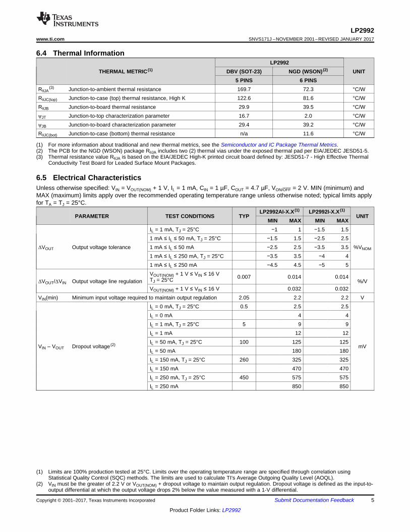
(1) For more information about traditional and new thermal metrics, see the Semiconductor and IC Package Thermal Metrics.(2) The PCB for the NGD (WSON) package RθJA includes two (2) thermal vias under the exposed thermal pad per EIA/JEDEC JESD51-5.(3) Thermal resistance value RθJA is based on the EIA/JEDEC High-K printed circuit board defined by: JESD51-7 - High Effective Thermal
Conductivity Test Board for Leaded Surface Mount Packages.
6.4 Thermal Information
THERMAL METRIC (1)LP2992
UNITDBV (SOT-23) NGD (WSON) (2)
5 PINS 6 PINSRθJA
(3) Junction-to-ambient thermal resistance 169.7 72.3 °C/WRθJC(top) Junction-to-case (top) thermal resistance, High K 122.6 81.6 °C/WRθJB Junction-to-board thermal resistance 29.9 39.5 °C/WψJT Junction-to-top characterization parameter 16.7 2.0 °C/WψJB Junction-to-board characterization parameter 29.4 39.2 °C/WRθJC(bot) Junction-to-case (bottom) thermal resistance n/a 11.6 °C/W
(1) Limits are 100% production tested at 25°C. Limits over the operating temperature range are specified through correlation usingStatistical Quality Control (SQC) methods. The limits are used to calculate TI's Average Outgoing Quality Level (AOQL).
(2) VIN must be the greater of 2.2 V or VOUT(NOM) + dropout voltage to maintain output regulation. Dropout voltage is defined as the input-to-output differential at which the output voltage drops 2% below the value measured with a 1-V differential.
6.5 Electrical CharacteristicsUnless otherwise specified: VIN = VOUT(NOM) + 1 V, IL = 1 mA, CIN = 1 µF, COUT = 4.7 µF, VON/OFF = 2 V. MIN (minimum) andMAX (maximum) limits apply over the recommended operating temperature range unless otherwise noted; typical limits applyfor TA = TJ = 25°C.
PARAMETER TEST CONDITIONS TYPLP2992AI-X.X (1) LP2992I-X.X (1)
UNITMIN MAX MIN MAX
ΔVOUT Output voltage tolerance
IL = 1 mA, TJ = 25°C −1 1 −1.5 1.5
%VNOM
1 mA ≤ IL ≤ 50 mA, TJ = 25°C −1.5 1.5 −2.5 2.51 mA ≤ IL ≤ 50 mA −2.5 2.5 −3.5 3.51 mA ≤ IL ≤ 250 mA, TJ = 25°C −3.5 3.5 −4 41 mA ≤ IL ≤ 250 mA −4.5 4.5 −5 5
ΔVOUT/ΔVIN Output voltage line regulationVOUT(NOM) + 1 V ≤ VIN ≤ 16 VTJ = 25°C 0.007 0.014 0.014
%/VVOUT(NOM) + 1 V ≤ VIN ≤ 16 V 0.032 0.032
VIN(min) Minimum input voltage required to maintain output regulation 2.05 2.2 2.2 V
VIN – VOUT Dropout voltage (2)
IL = 0 mA, TJ = 25°C 0.5 2.5 2.5
mV
IL = 0 mA 4 4IL = 1 mA, TJ = 25°C 5 9 9IL = 1 mA 12 12IL = 50 mA, TJ = 25°C 100 125 125IL = 50 mA 180 180IL = 150 mA, TJ = 25°C 260 325 325IL = 150 mA 470 470IL = 250 mA, TJ = 25°C 450 575 575IL = 250 mA 850 850

6
LP2992SNVS171J –NOVEMBER 2001–REVISED JANUARY 2017 www.ti.com
Product Folder Links: LP2992
Submit Documentation Feedback Copyright © 2001–2017, Texas Instruments Incorporated
Electrical Characteristics (continued)Unless otherwise specified: VIN = VOUT(NOM) + 1 V, IL = 1 mA, CIN = 1 µF, COUT = 4.7 µF, VON/OFF = 2 V. MIN (minimum) andMAX (maximum) limits apply over the recommended operating temperature range unless otherwise noted; typical limits applyfor TA = TJ = 25°C.
PARAMETER TEST CONDITIONS TYPLP2992AI-X.X (1) LP2992I-X.X (1)
UNITMIN MAX MIN MAX
(3) The ON/OFF input must be properly driven to prevent possible mis-operation. For details, see Operation with ON/OFF Control.(4) The LP2992 has thermal foldback current limiting which allows a high peak current when VOUT > 0.5 V, and then reduces the maximum
output current as VOUT is forced to ground (see Typical Characteristics curves).
IGND Ground pin current
IL = 0 mA, TJ = 25°C 65 95 95
µA
IL = 0 mA 125 125IL = 1 mA, TJ = 25°C 75 110 110IL = 1 mA 170 170IL = 50 mA, TJ = 25°C 350 600 600IL = 50 mA 1000 1000IL = 150 mA, TJ = 25°C 850 1500 1500IL = 150 mA 2500 2500IL = 250 mA, TJ = 25°C 1500 2300 2300IL = 250 mA 4000 4000VON/OFF < 0.3 V, TJ = 25°C 0.01 0.8 0.8VON/OFF < 0.15 V 0.05 2 2
VON/OFF ON/OFF input voltage (3) High = O/P ON 1.4 1.6 1.6V
Low = O/P OFF 0.55 0.15 0.15
ION/OFF ON/OFF input currentVON/OFF = 0 0.01 –2 –2
µAVON/OFF = 5 V 5 15 15
en Output noise voltage (RMS)Bandwidth = 300 Hz to 50 kHzCOUT = 10 µFCBYPASS = 10 nF
30 µV
ΔVOUT/ΔVIN Ripple rejection f = 1 kHz, CBYPASS = 10 nFCOUT = 10 µF 45 dB
IO(SC) Short-circuit current RL = 0 (steady state) (4) 400 mAIO(PK) Peak output current VOUT ≥ VO(NOM) – 5% 350 mA

7
LP2992www.ti.com SNVS171J –NOVEMBER 2001–REVISED JANUARY 2017
Product Folder Links: LP2992
Submit Documentation FeedbackCopyright © 2001–2017, Texas Instruments Incorporated
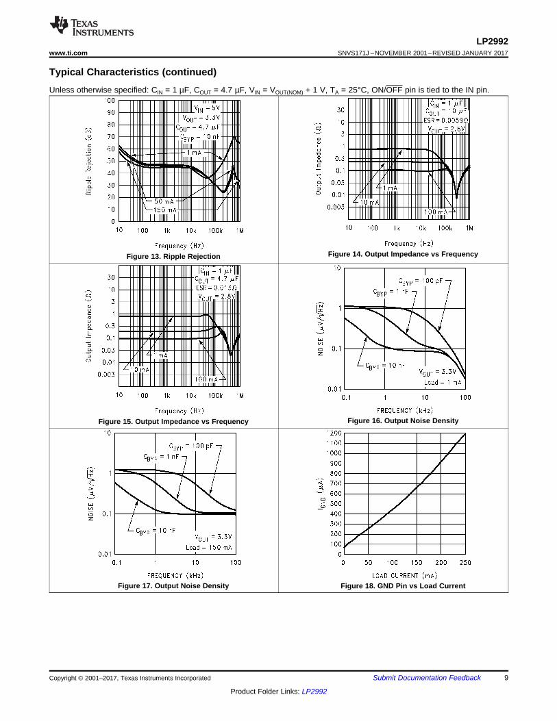
6.6 Typical CharacteristicsUnless otherwise specified: CIN = 1 µF, COUT = 4.7 µF, VIN = VOUT(NOM) + 1 V, TA = 25°C, ON/OFF pin is tied to the IN pin.
Figure 1. VOUT vs Temperature Figure 2. Short-Circuit Current
Figure 3. Short-Circuit Current Figure 4. Short-Circuit Current vs Output Voltage
Figure 5. Ripple Rejection Figure 6. Ripple Rejection

8
LP2992SNVS171J –NOVEMBER 2001–REVISED JANUARY 2017 www.ti.com
Product Folder Links: LP2992
Submit Documentation Feedback Copyright © 2001–2017, Texas Instruments Incorporated
Typical Characteristics (continued)Unless otherwise specified: CIN = 1 µF, COUT = 4.7 µF, VIN = VOUT(NOM) + 1 V, TA = 25°C, ON/OFF pin is tied to the IN pin.
Figure 7. Ripple Rejection Figure 8. Ripple Rejection
Figure 9. Ripple Rejection Figure 10. Ripple Rejection
Figure 11. Ripple Rejection Figure 12. Ripple Rejection
9
LP2992www.ti.com SNVS171J –NOVEMBER 2001–REVISED JANUARY 2017
Product Folder Links: LP2992
Submit Documentation FeedbackCopyright © 2001–2017, Texas Instruments Incorporated
Typical Characteristics (continued)Unless otherwise specified: CIN = 1 µF, COUT = 4.7 µF, VIN = VOUT(NOM) + 1 V, TA = 25°C, ON/OFF pin is tied to the IN pin.
Figure 13. Ripple Rejection Figure 14. Output Impedance vs Frequency
Figure 15. Output Impedance vs Frequency Figure 16. Output Noise Density
Figure 17. Output Noise Density Figure 18. GND Pin vs Load Current

10
LP2992SNVS171J –NOVEMBER 2001–REVISED JANUARY 2017 www.ti.com
Product Folder Links: LP2992
Submit Documentation Feedback Copyright © 2001–2017, Texas Instruments Incorporated
Typical Characteristics (continued)Unless otherwise specified: CIN = 1 µF, COUT = 4.7 µF, VIN = VOUT(NOM) + 1 V, TA = 25°C, ON/OFF pin is tied to the IN pin.
Figure 19. Dropout Voltage vs Temperature Figure 20. Input Current vs Pin
Figure 21. IGND vs Load and Temperature Figure 22. Instantaneous Short-Circuit Current
Figure 23. Load Transient Response Figure 24. Load Transient Response

11
LP2992www.ti.com SNVS171J –NOVEMBER 2001–REVISED JANUARY 2017
Product Folder Links: LP2992
Submit Documentation FeedbackCopyright © 2001–2017, Texas Instruments Incorporated
Typical Characteristics (continued)Unless otherwise specified: CIN = 1 µF, COUT = 4.7 µF, VIN = VOUT(NOM) + 1 V, TA = 25°C, ON/OFF pin is tied to the IN pin.
Figure 25. Load Transient Response Figure 26. Line Transient Response
Figure 27. Line Transient Response Figure 28. Line Transient Response
Figure 29. Line Transient Response Figure 30. Turnon Time
12
LP2992SNVS171J –NOVEMBER 2001–REVISED JANUARY 2017 www.ti.com
Product Folder Links: LP2992
Submit Documentation Feedback Copyright © 2001–2017, Texas Instruments Incorporated
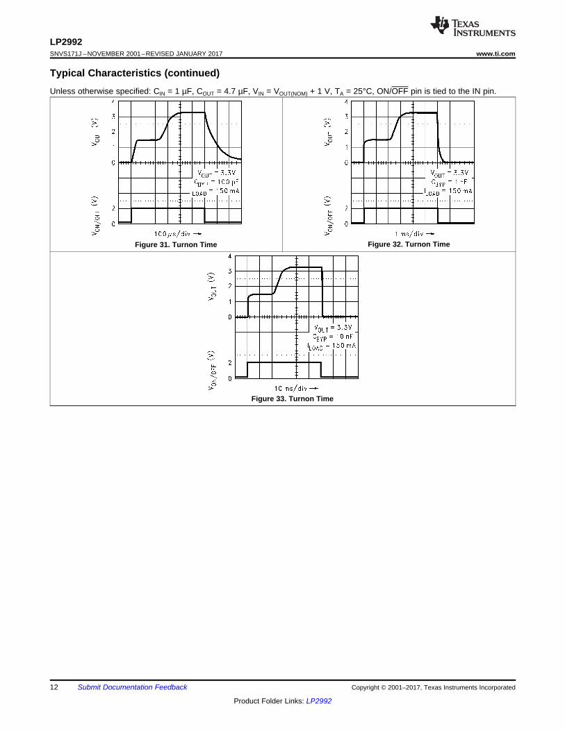
Typical Characteristics (continued)Unless otherwise specified: CIN = 1 µF, COUT = 4.7 µF, VIN = VOUT(NOM) + 1 V, TA = 25°C, ON/OFF pin is tied to the IN pin.
Figure 31. Turnon Time Figure 32. Turnon Time
Figure 33. Turnon Time

13
LP2992www.ti.com SNVS171J –NOVEMBER 2001–REVISED JANUARY 2017
Product Folder Links: LP2992
Submit Documentation FeedbackCopyright © 2001–2017, Texas Instruments Incorporated
7 Detailed Description
7.1 OverviewThe LP2992 family of fixed-output, ultralow-dropout, and low-noise regulators offer exceptional and cost-effectiveperformance for battery-powered applications. Available in output voltages from 1.5 V to 5 V, the family has anoutput tolerance of 1% for the A version and is capable of delivering 250-mA continuous load current. Using anoptimized vertically integrated PNP (VIP) process, the LP2992 delivers unequaled performance. The dropoutvoltage and the GND pin current with 250 mA of load current are typically 450 mV and 1500 µA, respectively.
7.2 Functional Block Diagram
7.3 Feature Description
7.3.1 Sleep ModeWhen the ON/OFF pin is pulled low, the LP2992 enters a sleep mode, and less than 1-µA quiescent current isconsumed. This function is designed for the application which needs a sleep mode to effectively enhance batterylife cycle.
7.3.2 Low Ground CurrentThe LP2992 uses a vertical PNP process which allows for quiescent currents which are considerably lower thanthose associated with traditional lateral PNP regulators, typically 1500 µA at 250-mA load and 75 µA at 1-mAload.
7.3.3 Low NoiseThe LP2992 includes a low-noise reference ensuring minimal noise during operation because the internalreference is normally the dominant term in a noise analysis. Further noise reduction can be achieved by addingan external bypass capacitor between the BYPASS pin and the GND pin. For more detailed information on noisereduction using the BYPASS pin, see Noise Bypass Capacitor.
7.3.4 Enhanced StabilityThe LP2992 is designed specifically to work with ceramic output capacitors using circuitry that allows theregulator to be stable across the entire range of output current with an output capacitor whose ESR is as low as5 mΩ. For output capacitor requirements, see Output Capacitor.
14
LP2992SNVS171J –NOVEMBER 2001–REVISED JANUARY 2017 www.ti.com
Product Folder Links: LP2992
Submit Documentation Feedback Copyright © 2001–2017, Texas Instruments Incorporated
Feature Description (continued)7.3.5 Overcurrent ProtectionThe internal current-limit circuit is used to protect the LDO against high-current faults or shorting events. TheLDO is not designed to operate in a steady-state current limit. During a current-limit event, the LDO sourcesconstant current. Therefore, the output voltage falls when the output impedance decreases. Note also that if acurrent limit occurs and the resulting output voltage is low, excessive power may be dissipated across the LDO,resulting in a thermal shutdown of the output.
The LP2992 is featured with the foldback current limit that allows a high peak current when VOUT > 0.5 V, andthen reduces the maximum output current as VOUT is forced to ground.
7.3.6 Overtemperature ProtectionThe LP2992 is designed with the thermal shutdown circuitry to turn off the output when excessive heat isdissipated in the LDO. The internal protection circuitry of the LP2992 is designed to protect against thermaloverload conditions. Continuously running the device into thermal shutdown degrades its reliability.
7.4 Device Functional Modes
7.4.1 Operation with VOUT(TARGET) + 0.9 V ≥ VIN ≥ 16 VThe LP2992 operates if the input voltage is equal to or exceeds VOUT(TARGET) + 0.9 V. At input voltages below theminimum VIN requirement, the device does not operate correctly and output voltage may not reach a target value.
7.4.2 Operation with ON/OFF ControlIf the voltage on the ON/OFF pin is less than 0.15 V, the device is disabled and, in this shutdown state, currentdoes not exceed 2 µA. Raising the voltage at the ON/OFF pin above 1.6 V initiates the start-up sequence of thedevice. If this feature is not to be used, the ON/OFF input must be tied to VIN to keep the regulator output on atall times.
To assure proper operation, the signal source used to drive the ON/OFF input must be able to swing above andbelow the specified turnon/turnoff voltage thresholds listed in the Electrical Characteristics section under VON/OFF.To prevent mis-operation, the turnon (and turnoff) voltage signals applied to the ON/OFF input must have a slewrate which is ≥ 40 mV/µs.
CAUTIONThe regulator output voltage can not be ensured if a slow-moving AC (or DC) signal isapplied that is in the range between the specified turnon and turnoff voltages listedunder the electrical specification VON/OFF (see Electrical Characteristics).

15
LP2992www.ti.com SNVS171J –NOVEMBER 2001–REVISED JANUARY 2017
Product Folder Links: LP2992
Submit Documentation FeedbackCopyright © 2001–2017, Texas Instruments Incorporated
8 Application and Implementation
NOTEInformation in the following applications sections is not part of the TI componentspecification, and TI does not warrant its accuracy or completeness. TI’s customers areresponsible for determining suitability of components for their purposes. Customers shouldvalidate and test their design implementation to confirm system functionality.
8.1 Application InformationThe LP2992 is a 250-mA, fixed-output voltage regulator designed to provide ultralow-dropout and low noise inbattery powered applications. The device is stable with output capacitor equivalent series resistance (ESR) aslow as 5 mΩ which allows the use of ceramic capacitors on the output.
At 250-mA loading, the dropout voltage of the LP2992 is 850 mV maximum over temperature; thus, 1000-mVheadroom is sufficient for operation over input and output voltage accuracy. The efficiency of the LP2992 in thisconfiguration is VOUT/VIN = 76.7%. To achieve the smallest form factor, the SOT-23 package is selected.
Input and output capacitors are selected in accordance with Capacitor Characteristics. Ceramic capacitance of1 µF for the input and that of 4.7 µF for the output are selected. With efficiency of 76.7% and a 250-mA loadcurrent, the internal power dissipation is 250 mW, which corresponds to 43.55°C junction temperature rise for theSOT-23 package. To minimize noise, a bypass capacitor (CBYPASS) of 0.01 µF is selected.
8.2 Typical Application
*ON/OFF input must be actively terminated. Tie to the IN pin if this function is not to be used.**Minimum capacitance is shown to ensure stability (may be increased without limit). Ceramic capacitor required foroutput (see Output Capacitor).***Reduces output noise (may be omitted if application is not noise critical). Use ceramic or film type with very lowleakage current (see Capacitor Characteristics).
Figure 34. Basic Application Circuit

16
LP2992SNVS171J –NOVEMBER 2001–REVISED JANUARY 2017 www.ti.com
Product Folder Links: LP2992
Submit Documentation Feedback Copyright © 2001–2017, Texas Instruments Incorporated
Typical Application (continued)8.2.1 Design RequirementsFor basic design parameters, see Table 1.
Table 1. Design ParametersDESIGN PARAMETER VALUE
Input voltage 4.3 VOutput voltage 3.3 V
Output current 150 mA (maximum)1 mA (minimum)
Output capacitor range 4.7 µF
8.2.2 Detailed Design Procedure
8.2.2.1 External CapacitorsLike any low-dropout regulator, the LP2992 requires external capacitors for regulator stability. These capacitorsmust be correctly selected for good performance.
8.2.2.1.1 Input Capacitor
An input capacitor whose capacitance is ≥ 1 µF is required between the LP2992 input and ground (the amount ofcapacitance may be increased without limit).
This capacitor must be located a distance of not more than 1 cm from the IN pin and returned to a clean analogground. Any good quality ceramic, tantalum, or film capacitor may be used at the input.
NOTETantalum capacitors can suffer catastrophic failure due to surge current when connectedto a low-impedance source of power (like a battery or very large capacitor). If a tantalumcapacitor is used at the input, it must be specified by the manufacturer to have a surgecurrent rating sufficient for the application.
There are no requirements for ESR on the input capacitor, but tolerance and temperature coefficient must beconsidered when selecting the capacitor to ensure the capacitance is ≥ 1 µF over the entire operatingtemperature range.
8.2.2.1.2 Output Capacitor
The LP2992 is designed specifically to work with ceramic output capacitors, using circuitry that allows theregulator to be stable across the entire range of output current with an output capacitor whose ESR is as low as5 mΩ. It may also be possible to use tantalum or film capacitors at the output, but these are not as attractive forreasons of size and cost (see Capacitor Characteristics).
The output capacitor must meet the requirement for minimum amount of capacitance and also have an ESRvalue which is within the stable range. Curves are provided which show the stable ESR range as a function ofload current (see Figure 35).

17
LP2992www.ti.com SNVS171J –NOVEMBER 2001–REVISED JANUARY 2017
Product Folder Links: LP2992
Submit Documentation FeedbackCopyright © 2001–2017, Texas Instruments Incorporated
Figure 35. Stable ESR Range vs Load Current
The output capacitor must maintain its ESR within the stable region over the full operating temperature range ofthe application to assure stability.
The LP2992 requires a minimum of 4.7 µF on the output (output capacitor size can be increased without limit).
It is important to remember that capacitor tolerance and variation with temperature must be taken intoconsideration when selecting an output capacitor so that the minimum required amount of output capacitance isprovided over the full operating temperature range. It must be noted that ceramic capacitors can exhibit largechanges in capacitance with temperature (see Capacitor Characteristics).
The output capacitor must be located not more than 1 cm from the output pin and returned to a clean analogground.
8.2.2.1.3 Noise Bypass Capacitor
Connecting a 10-nF capacitor to the BYPASS pin significantly reduces noise on the regulator output. It should benoted that the capacitor is connected directly to a high-impedance circuit in the bandgap reference.
Because this circuit has only a few microamperes flowing in it, any significant loading on this node causes achange in the regulated output voltage. For this reason, dc leakage current through the noise bypass capacitormust never exceed 100 nA, and must be kept as low as possible for best output voltage accuracy.
The types of capacitors best suited for the noise bypass capacitor are ceramic and film. High-quality ceramiccapacitors with either NPO or COG dielectric typically have very low leakage. 10-nF polypropolene andpolycarbonate film capacitors are available in small surface-mount packages and typically have extremely lowleakage current.
8.2.2.2 Capacitor CharacteristicsThe LP2992 was designed to work with ceramic capacitors on the output to take advantage of the benefits theyoffer. For capacitance values in the 2.2-µF to 10-µF range, ceramics are the least expensive and also have thelowest ESR values (which makes them best for eliminating high-frequency noise). The ESR of a typical 4.7-µFceramic capacitor is in the range of 5 mΩ to 10 mΩ, which easily meets the ESR limits required for stability bythe LP2992.
One disadvantage of ceramic capacitors is that their capacitance can vary with temperature. Most large valueceramic capacitors (≥ 2.2 µF) are manufactured with the Z5U or Y5V temperature characteristic, which results inthe capacitance dropping by more than 50% as the temperature goes from 25°C to 85°C.
This could cause problems if a 4.7-µF capacitor were used on the output because it drops down to approximately2.3 µF at high ambient temperatures (which could cause the LP2992 to oscillate). If Z5U or Y5V capacitors areused on the output, a minimum capacitance value of 10 µF must be observed.
A better choice for temperature coefficient in ceramic capacitors is X7R, which holds the capacitance within±15%. Unfortunately, the larger values of capacitance are not offered by all manufacturers in the X7R dielectric.

18
LP2992SNVS171J –NOVEMBER 2001–REVISED JANUARY 2017 www.ti.com
Product Folder Links: LP2992
Submit Documentation Feedback Copyright © 2001–2017, Texas Instruments Incorporated
8.2.2.2.1 Tantalum
Tantalum capacitors are less desirable than ceramics for use as output capacitors because they are moreexpensive when comparing equivalent capacitance and voltage ratings in the 1-µF to 4.7-µF range.
Another important consideration is that tantalum capacitors have higher ESR values than equivalent sizeceramics. This means that while it may be possible to find a Tantalum capacitor with an ESR value within thestable range, it would have to be larger in capacitance (which means bigger and more costly) than a ceramiccapacitor with the same ESR value.
It should also be noted that the ESR of a typical tantalum increases about 2:1 as the temperature goes from25°C down to −40°C, so some guard band must be allowed.
8.2.2.3 Reverse Input-Output VoltageThe PNP power transistor used as the pass element in the LP2992 has an inherent diode connected betweenthe regulator output and input. During normal operation (where the input voltage is higher than the output) thisdiode is reverse-biased.
However, if the output is pulled above the input, this diode turns ON and current flows into the regulator output.In such cases, a parasitic SCR can latch which allows a high current to flow into VIN (and out the ground pin),which can damage the part.
In any application where the output may be pulled above the input, an external Schottky diode must beconnected from VIN to VOUT (cathode on VIN, anode on VOUT), to limit the reverse voltage across the LP2992 to0.3 V (see Absolute Maximum Ratings).
8.2.2.4 Power DissipationKnowing the device power dissipation and proper sizing of the thermal plane connected to the tab or pad iscritical to ensuring reliable operation. Device power dissipation depends on input voltage, output voltage, andload conditions and can be calculated with Equation 1.
PD(MAX) = (VIN(MAX) – VOUT) × IOUT (1)
Power dissipation can be minimized, and greater efficiency can be achieved, by using the lowest availablevoltage drop option that would still be greater than the dropout voltage (VDO). However, keep in mind that highervoltage drops result in better dynamic (that is, PSRR and transient) performance.
On the WSON (NGD) package, the primary conduction path for heat is through the exposed power pad to thePCB. To ensure the device does not overheat, connect the exposed pad, through thermal vias, to an internalground plane with an appropriate amount of copper PCB area.
On the SOT-23 (DBV) package, the primary conduction path for heat is through the pins to the PCB. Themaximum allowable junction temperature (TJ(MAX))determines maximum power dissipation allowed (PD(MAX)) forthe device package.
Power dissipation and junction temperature are most often related by the junction-to-ambient thermal resistance(RθJA) of the combined PCB and device package and the temperature of the ambient air (TA), according toEquation 2 or Equation 2:
TJ(MAX) = TA(MAX) + ( RθJA × PD(MAX)) (2)PD = TJ(MAX) – TA(MAX) / RθJA (3)
Unfortunately, this RθJA is highly dependent on the heat-spreading capability of the particular PCB design, andtherefore varies according to the total copper area, copper weight, and location of the planes. The RθJA recordedin Thermal Information is determined by the specific EIA/JEDEC JESD51-7 standard for PCB and copper-spreading area, and is to be used only as a relative measure of package thermal performance. For a well-designed thermal layout, RθJA is actually the sum of the package junction-to-case (bottom) thermal resistance(RθJCbot) plus the thermal resistance contribution by the PCB copper area acting as a heat sink.

19
LP2992www.ti.com SNVS171J –NOVEMBER 2001–REVISED JANUARY 2017
Product Folder Links: LP2992
Submit Documentation FeedbackCopyright © 2001–2017, Texas Instruments Incorporated
8.2.2.5 Estimating Junction TemperatureThe EIA/JEDEC standard recommends the use of psi (Ψ) thermal characteristics to estimate the junctiontemperatures of surface mount devices on a typical PCB board application. These characteristics are not truethermal resistance values, but rather package specific thermal characteristics that offer practical and relativemeans of estimating junction temperatures. These psi metrics are determined to be significantly independent ofcopper-spreading area. The key thermal characteristics (ΨJT and ΨJB) are given in Thermal Information and areused in accordance with Equation 4 or Equation 5.
TJ(MAX) = TTOP + (ΨJT × PD(MAX))
where• PD(MAX) is explained in Equation 3• TTOP is the temperature measured at the center-top of the device package. (4)
TJ(MAX) = TBOARD + (ΨJB × PD(MAX))
where• PD(MAX) is explained in Equation 3.• TBOARD is the PCB surface temperature measured 1-mm from the device package and centered on the
package edge. (5)
For more information about the thermal characteristics ΨJT and ΨJB, see Semiconductor and IC Package ThermalMetrics; for more information about measuring TTOP and TBOARD, Using New Thermal Metrics (SBVA025); and formore information about the EIA/JEDEC JESD51 PCB used for validating RθJA, see Thermal Characteristics ofLinear and Logic Packages Using JEDEC PCB Designs. These application notes are available at www.ti.com.

20
LP2992SNVS171J –NOVEMBER 2001–REVISED JANUARY 2017 www.ti.com
Product Folder Links: LP2992
Submit Documentation Feedback Copyright © 2001–2017, Texas Instruments Incorporated
8.2.3 Application Curves
Figure 36. Load Transient Response Figure 37. Load Transient Response
Figure 38. Line Transient Response Figure 39. Line Transient Response
Figure 40. Turnon Time Figure 41. Turnon Time
9 Power Supply RecommendationsThe LP2992 is designed to operate from an input voltage supply range from 2.2 V to 16 V. The input voltagerange provides the adequate headroom in order for the device to have a regulated output. This input supply mustbe well regulated. If the input supply is noisy, additional input capacitors with low ESR can help to improve theoutput noise performance.

GND
VIN
VOUT
COUT
1
2
3
6
5
4
CIN
VBYPASS
VON/OFF
CBYPASS
Power Ground
IN
GND
ON/OFF
OUT
BYPASS
COUT1
3 4
5VIN
VON/OFF
VOUT
CIN
Power Ground2
CBYPASS
21
LP2992www.ti.com SNVS171J –NOVEMBER 2001–REVISED JANUARY 2017
Product Folder Links: LP2992
Submit Documentation FeedbackCopyright © 2001–2017, Texas Instruments Incorporated
10 Layout
10.1 Layout GuidelinesFor best overall performance, place all circuit components on the same side of the circuit board and as near aspractical to the respective LDO pin connections. Place ground return connections to the input and outputcapacitors, and to the LDO ground pin as close as possible to each other, connected by a wide, component-side,copper surface. The use of vias and long traces to create LDO circuit connections is strongly discouraged andnegatively affects system performance. This grounding and layout scheme minimizes inductive parasitics, andthereby reduces load-current transients, minimizes noise, and increases circuit stability.
TI also recommends a ground reference plane either embedded in the PCB itself or located on the bottom side ofthe PCB opposite the components. This reference plane serves to assure accuracy of the output voltage, shieldnoise, and behaves similar to a thermal plane to spread (or sink) heat from the LDO device. In most applications,this ground plane is necessary to meet thermal requirements.
10.2 Layout Examples
Figure 42. LP2992 SOT-23 Package Typical Layout
Figure 43. LP2992 WSON Package Typical Layout
10.3 WSON MountingThe WSON package requires specific mounting techniques which are detailed in AN-1187 Leadless LeadframePackage (LLP). Referring to the section PCB Design Recommendations, note that the pad style which must beused with the WSON package is the NSMD (non-solder mask defined) type.
The thermal dissipation of the WSON package is directly related to the printed circuit board construction and theamount of additional copper area.

22
LP2992SNVS171J –NOVEMBER 2001–REVISED JANUARY 2017 www.ti.com
Product Folder Links: LP2992
Submit Documentation Feedback Copyright © 2001–2017, Texas Instruments Incorporated
11 Device and Documentation Support
11.1 Documentation Support
11.1.1 Related DocumentationFor related documentation see the following:• AN-1187 Leadless Leadframe Package (LLP)• Semiconductor and IC Package Thermal Metrics• Using New Thermal Metrics (SBVA025)• Thermal Characteristics of Linear and Logic Packages Using JEDEC PCB Designs
11.2 Receiving Notification of Documentation UpdatesTo receive notification of documentation updates, navigate to the device product folder on ti.com. In the upperright corner, click on Alert me to register and receive a weekly digest of any product information that haschanged. For change details, review the revision history included in any revised document.
11.3 Community ResourcesThe following links connect to TI community resources. Linked contents are provided "AS IS" by the respectivecontributors. They do not constitute TI specifications and do not necessarily reflect TI's views; see TI's Terms ofUse.
TI E2E™ Online Community TI's Engineer-to-Engineer (E2E) Community. Created to foster collaborationamong engineers. At e2e.ti.com, you can ask questions, share knowledge, explore ideas and helpsolve problems with fellow engineers.
Design Support TI's Design Support Quickly find helpful E2E forums along with design support tools andcontact information for technical support.
11.4 TrademarksE2E is a trademark of Texas Instruments.All other trademarks are the property of their respective owners.
11.5 Electrostatic Discharge CautionThese devices have limited built-in ESD protection. The leads should be shorted together or the device placed in conductive foamduring storage or handling to prevent electrostatic damage to the MOS gates.
11.6 GlossarySLYZ022 — TI Glossary.
This glossary lists and explains terms, acronyms, and definitions.
12 Mechanical, Packaging, and Orderable InformationThe following pages include mechanical, packaging, and orderable information. This information is the mostcurrent data available for the designated devices. This data is subject to change without notice and revision ofthis document. For browser-based versions of this data sheet, refer to the left-hand navigation.

PACKAGE OPTION ADDENDUM
www.ti.com 14-Oct-2017
Addendum-Page 1
PACKAGING INFORMATION
Orderable Device Status(1)
Package Type PackageDrawing
Pins PackageQty
Eco Plan(2)
Lead/Ball Finish(6)
MSL Peak Temp(3)
Op Temp (°C) Device Marking(4/5)
Samples
LP2992AILD-1.5/NOPB ACTIVE WSON NGD 6 1000 Green (RoHS& no Sb/Br)
CU SN Level-3-260C-168 HR -40 to 125 L011A
LP2992AILD-1.8/NOPB ACTIVE WSON NGD 6 1000 Green (RoHS& no Sb/Br)
CU NIPDAU | CU SN Level-3-260C-168 HR -40 to 125 L012A
LP2992AILD-3.3/NOPB ACTIVE WSON NGD 6 1000 Green (RoHS& no Sb/Br)
CU NIPDAU | CU SN Level-3-260C-168 HR -40 to 125 L014A
LP2992AILD-5.0/NOPB ACTIVE WSON NGD 6 1000 Green (RoHS& no Sb/Br)
CU NIPDAU | CU SN Level-3-260C-168 HR -40 to 125 L015A
LP2992AILDX-3.3/NOPB ACTIVE WSON NGD 6 4500 Green (RoHS& no Sb/Br)
CU NIPDAU | CU SN Level-3-260C-168 HR -40 to 125 L014A
LP2992AILDX-5.0/NOPB ACTIVE WSON NGD 6 4500 Green (RoHS& no Sb/Br)
CU NIPDAU | CU SN Level-3-260C-168 HR -40 to 125 L015A
LP2992AIM5-1.5/NOPB ACTIVE SOT-23 DBV 5 1000 Green (RoHS& no Sb/Br)
CU SN Level-1-260C-UNLIM -40 to 125 LFBA
LP2992AIM5-1.8/NOPB ACTIVE SOT-23 DBV 5 1000 Green (RoHS& no Sb/Br)
CU SN Level-1-260C-UNLIM -40 to 125 LFCA
LP2992AIM5-2.5 NRND SOT-23 DBV 5 1000 TBD Call TI Call TI -40 to 125 LFDA
LP2992AIM5-2.5/NOPB ACTIVE SOT-23 DBV 5 1000 Green (RoHS& no Sb/Br)
CU SN Level-1-260C-UNLIM -40 to 125 LFDA
LP2992AIM5-3.3 NRND SOT-23 DBV 5 1000 TBD Call TI Call TI -40 to 125 LFEA
LP2992AIM5-3.3/NOPB ACTIVE SOT-23 DBV 5 1000 Green (RoHS& no Sb/Br)
CU SN Level-1-260C-UNLIM -40 to 125 LFEA
LP2992AIM5-5.0/NOPB ACTIVE SOT-23 DBV 5 1000 Green (RoHS& no Sb/Br)
CU SN Level-1-260C-UNLIM -40 to 125 LFFA
LP2992AIM5X-1.5/NOPB ACTIVE SOT-23 DBV 5 3000 Green (RoHS& no Sb/Br)
CU SN Level-1-260C-UNLIM -40 to 125 LFBA
LP2992AIM5X-1.8/NOPB ACTIVE SOT-23 DBV 5 3000 Green (RoHS& no Sb/Br)
CU SN Level-1-260C-UNLIM -40 to 125 LFCA
LP2992AIM5X-2.5/NOPB ACTIVE SOT-23 DBV 5 3000 Green (RoHS& no Sb/Br)
CU SN Level-1-260C-UNLIM -40 to 125 LFDA
LP2992AIM5X-3.3/NOPB ACTIVE SOT-23 DBV 5 3000 Green (RoHS& no Sb/Br)
CU SN Level-1-260C-UNLIM -40 to 125 LFEA
LP2992AIM5X-5.0/NOPB ACTIVE SOT-23 DBV 5 3000 Green (RoHS& no Sb/Br)
CU SN Level-1-260C-UNLIM -40 to 125 LFFA

PACKAGE OPTION ADDENDUM
www.ti.com 14-Oct-2017
Addendum-Page 2
Orderable Device Status(1)
Package Type PackageDrawing
Pins PackageQty
Eco Plan(2)
Lead/Ball Finish(6)
MSL Peak Temp(3)
Op Temp (°C) Device Marking(4/5)
Samples
LP2992ILD-1.8/NOPB ACTIVE WSON NGD 6 1000 Green (RoHS& no Sb/Br)
CU NIPDAU | CU SN Level-3-260C-168 HR -40 to 125 L012AB
LP2992ILD-2.5/NOPB ACTIVE WSON NGD 6 1000 Green (RoHS& no Sb/Br)
CU SN Level-3-260C-168 HR -40 to 125 L013AB
LP2992ILD-3.3/NOPB ACTIVE WSON NGD 6 1000 Green (RoHS& no Sb/Br)
CU NIPDAU | CU SN Level-3-260C-168 HR -40 to 125 L014AB
LP2992ILD-5.0/NOPB ACTIVE WSON NGD 6 1000 Green (RoHS& no Sb/Br)
CU NIPDAU | CU SN Level-3-260C-168 HR -40 to 125 L015AB
LP2992ILDX-1.5/NOPB ACTIVE WSON NGD 6 4500 Green (RoHS& no Sb/Br)
CU NIPDAU | CU SN Level-3-260C-168 HR -40 to 125 L011AB
LP2992ILDX-3.3/NOPB ACTIVE WSON NGD 6 4500 Green (RoHS& no Sb/Br)
CU NIPDAU | CU SN Level-3-260C-168 HR -40 to 125 L014AB
LP2992ILDX-5.0/NOPB ACTIVE WSON NGD 6 4500 Green (RoHS& no Sb/Br)
CU SN Level-3-260C-168 HR -40 to 125 L015AB
LP2992IM5-1.5/NOPB ACTIVE SOT-23 DBV 5 1000 Green (RoHS& no Sb/Br)
CU SN Level-1-260C-UNLIM -40 to 125 LFBB
LP2992IM5-1.8 NRND SOT-23 DBV 5 1000 TBD Call TI Call TI -40 to 125 LFCB
LP2992IM5-1.8/NOPB ACTIVE SOT-23 DBV 5 1000 Green (RoHS& no Sb/Br)
CU SN Level-1-260C-UNLIM -40 to 125 LFCB
LP2992IM5-2.5 NRND SOT-23 DBV 5 1000 TBD Call TI Call TI -40 to 125 LFDB
LP2992IM5-2.5/NOPB ACTIVE SOT-23 DBV 5 1000 Green (RoHS& no Sb/Br)
CU SN Level-1-260C-UNLIM -40 to 125 LFDB
LP2992IM5-3.0 NRND SOT-23 DBV 5 1000 TBD Call TI Call TI LF8B
LP2992IM5-3.0/NOPB ACTIVE SOT-23 DBV 5 1000 Green (RoHS& no Sb/Br)
CU SN Level-1-260C-UNLIM LF8B
LP2992IM5-3.3 NRND SOT-23 DBV 5 1000 TBD Call TI Call TI -40 to 125 LFEB
LP2992IM5-3.3/NOPB ACTIVE SOT-23 DBV 5 1000 Green (RoHS& no Sb/Br)
CU SN Level-1-260C-UNLIM -40 to 125 LFEB
LP2992IM5-5.0/NOPB ACTIVE SOT-23 DBV 5 1000 Green (RoHS& no Sb/Br)
CU SN Level-1-260C-UNLIM -40 to 125 LFFB
LP2992IM5X-1.5/NOPB ACTIVE SOT-23 DBV 5 3000 Green (RoHS& no Sb/Br)
CU SN Level-1-260C-UNLIM -40 to 125 LFBB
LP2992IM5X-1.8/NOPB ACTIVE SOT-23 DBV 5 3000 Green (RoHS& no Sb/Br)
CU SN Level-1-260C-UNLIM -40 to 125 LFCB
LP2992IM5X-2.5/NOPB ACTIVE SOT-23 DBV 5 3000 Green (RoHS& no Sb/Br)
CU SN Level-1-260C-UNLIM -40 to 125 LFDB

PACKAGE OPTION ADDENDUM
www.ti.com 14-Oct-2017
Addendum-Page 3
Orderable Device Status(1)
Package Type PackageDrawing
Pins PackageQty
Eco Plan(2)
Lead/Ball Finish(6)
MSL Peak Temp(3)
Op Temp (°C) Device Marking(4/5)
Samples
LP2992IM5X-3.3/NOPB ACTIVE SOT-23 DBV 5 3000 Green (RoHS& no Sb/Br)
CU SN Level-1-260C-UNLIM -40 to 125 LFEB
LP2992IM5X-5.0/NOPB ACTIVE SOT-23 DBV 5 3000 Green (RoHS& no Sb/Br)
CU SN Level-1-260C-UNLIM -40 to 125 LFFB
(1) The marketing status values are defined as follows:ACTIVE: Product device recommended for new designs.LIFEBUY: TI has announced that the device will be discontinued, and a lifetime-buy period is in effect.NRND: Not recommended for new designs. Device is in production to support existing customers, but TI does not recommend using this part in a new design.PREVIEW: Device has been announced but is not in production. Samples may or may not be available.OBSOLETE: TI has discontinued the production of the device.
(2) RoHS: TI defines "RoHS" to mean semiconductor products that are compliant with the current EU RoHS requirements for all 10 RoHS substances, including the requirement that RoHS substancedo not exceed 0.1% by weight in homogeneous materials. Where designed to be soldered at high temperatures, "RoHS" products are suitable for use in specified lead-free processes. TI mayreference these types of products as "Pb-Free".RoHS Exempt: TI defines "RoHS Exempt" to mean products that contain lead but are compliant with EU RoHS pursuant to a specific EU RoHS exemption.Green: TI defines "Green" to mean the content of Chlorine (Cl) and Bromine (Br) based flame retardants meet JS709B low halogen requirements of <=1000ppm threshold. Antimony trioxide basedflame retardants must also meet the <=1000ppm threshold requirement.
(3) MSL, Peak Temp. - The Moisture Sensitivity Level rating according to the JEDEC industry standard classifications, and peak solder temperature.
(4) There may be additional marking, which relates to the logo, the lot trace code information, or the environmental category on the device.
(5) Multiple Device Markings will be inside parentheses. Only one Device Marking contained in parentheses and separated by a "~" will appear on a device. If a line is indented then it is a continuationof the previous line and the two combined represent the entire Device Marking for that device.
(6) Lead/Ball Finish - Orderable Devices may have multiple material finish options. Finish options are separated by a vertical ruled line. Lead/Ball Finish values may wrap to two lines if the finishvalue exceeds the maximum column width.
Important Information and Disclaimer:The information provided on this page represents TI's knowledge and belief as of the date that it is provided. TI bases its knowledge and belief on informationprovided by third parties, and makes no representation or warranty as to the accuracy of such information. Efforts are underway to better integrate information from third parties. TI has taken andcontinues to take reasonable steps to provide representative and accurate information but may not have conducted destructive testing or chemical analysis on incoming materials and chemicals.TI and TI suppliers consider certain information to be proprietary, and thus CAS numbers and other limited information may not be available for release.
In no event shall TI's liability arising out of such information exceed the total purchase price of the TI part(s) at issue in this document sold by TI to Customer on an annual basis.
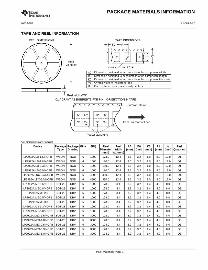
TAPE AND REEL INFORMATION
*All dimensions are nominal
Device PackageType
PackageDrawing
Pins SPQ ReelDiameter
(mm)
ReelWidth
W1 (mm)
A0(mm)
B0(mm)
K0(mm)
P1(mm)
W(mm)
Pin1Quadrant
LP2992AILD-1.5/NOPB WSON NGD 6 1000 178.0 12.4 3.6 3.2 1.0 8.0 12.0 Q1
LP2992AILD-1.8/NOPB WSON NGD 6 1000 180.0 12.4 3.6 3.2 1.0 8.0 12.0 Q1
LP2992AILD-3.3/NOPB WSON NGD 6 1000 180.0 12.4 3.6 3.2 1.0 8.0 12.0 Q1
LP2992AILD-5.0/NOPB WSON NGD 6 1000 180.0 12.4 3.6 3.2 1.0 8.0 12.0 Q1
LP2992AILDX-3.3/NOPB WSON NGD 6 4500 330.0 12.4 3.6 3.2 1.0 8.0 12.0 Q1
LP2992AILDX-5.0/NOPB WSON NGD 6 4500 330.0 12.4 3.6 3.2 1.0 8.0 12.0 Q1
LP2992AIM5-1.5/NOPB SOT-23 DBV 5 1000 178.0 8.4 3.2 3.2 1.4 4.0 8.0 Q3
LP2992AIM5-1.8/NOPB SOT-23 DBV 5 1000 178.0 8.4 3.2 3.2 1.4 4.0 8.0 Q3
LP2992AIM5-2.5 SOT-23 DBV 5 1000 178.0 8.4 3.2 3.2 1.4 4.0 8.0 Q3
LP2992AIM5-2.5/NOPB SOT-23 DBV 5 1000 178.0 8.4 3.2 3.2 1.4 4.0 8.0 Q3
LP2992AIM5-3.3 SOT-23 DBV 5 1000 178.0 8.4 3.2 3.2 1.4 4.0 8.0 Q3
LP2992AIM5-3.3/NOPB SOT-23 DBV 5 1000 178.0 8.4 3.2 3.2 1.4 4.0 8.0 Q3
LP2992AIM5-5.0/NOPB SOT-23 DBV 5 1000 178.0 8.4 3.2 3.2 1.4 4.0 8.0 Q3
LP2992AIM5X-1.5/NOPB SOT-23 DBV 5 3000 178.0 8.4 3.2 3.2 1.4 4.0 8.0 Q3
LP2992AIM5X-1.8/NOPB SOT-23 DBV 5 3000 178.0 8.4 3.2 3.2 1.4 4.0 8.0 Q3
LP2992AIM5X-2.5/NOPB SOT-23 DBV 5 3000 178.0 8.4 3.2 3.2 1.4 4.0 8.0 Q3
LP2992AIM5X-3.3/NOPB SOT-23 DBV 5 3000 178.0 8.4 3.2 3.2 1.4 4.0 8.0 Q3
LP2992AIM5X-5.0/NOPB SOT-23 DBV 5 3000 178.0 8.4 3.2 3.2 1.4 4.0 8.0 Q3
PACKAGE MATERIALS INFORMATION
www.ti.com 24-Aug-2017
Pack Materials-Page 1

Device PackageType
PackageDrawing
Pins SPQ ReelDiameter
(mm)
ReelWidth
W1 (mm)
A0(mm)
B0(mm)
K0(mm)
P1(mm)
W(mm)
Pin1Quadrant
LP2992ILD-1.8/NOPB WSON NGD 6 1000 180.0 12.4 3.6 3.2 1.0 8.0 12.0 Q1
LP2992ILD-2.5/NOPB WSON NGD 6 1000 178.0 12.4 3.6 3.2 1.0 8.0 12.0 Q1
LP2992ILD-3.3/NOPB WSON NGD 6 1000 180.0 12.4 3.6 3.2 1.0 8.0 12.0 Q1
LP2992ILD-5.0/NOPB WSON NGD 6 1000 180.0 12.4 3.6 3.2 1.0 8.0 12.0 Q1
LP2992ILDX-1.5/NOPB WSON NGD 6 4500 330.0 12.4 3.6 3.2 1.0 8.0 12.0 Q1
LP2992ILDX-3.3/NOPB WSON NGD 6 4500 330.0 12.4 3.6 3.2 1.0 8.0 12.0 Q1
LP2992ILDX-5.0/NOPB WSON NGD 6 4500 330.0 12.4 3.6 3.2 1.0 8.0 12.0 Q1
LP2992IM5-1.5/NOPB SOT-23 DBV 5 1000 178.0 8.4 3.2 3.2 1.4 4.0 8.0 Q3
LP2992IM5-1.8 SOT-23 DBV 5 1000 178.0 8.4 3.2 3.2 1.4 4.0 8.0 Q3
LP2992IM5-1.8/NOPB SOT-23 DBV 5 1000 178.0 8.4 3.2 3.2 1.4 4.0 8.0 Q3
LP2992IM5-2.5 SOT-23 DBV 5 1000 178.0 8.4 3.2 3.2 1.4 4.0 8.0 Q3
LP2992IM5-2.5/NOPB SOT-23 DBV 5 1000 178.0 8.4 3.2 3.2 1.4 4.0 8.0 Q3
LP2992IM5-3.0 SOT-23 DBV 5 1000 178.0 8.4 3.2 3.2 1.4 4.0 8.0 Q3
LP2992IM5-3.0/NOPB SOT-23 DBV 5 1000 178.0 8.4 3.2 3.2 1.4 4.0 8.0 Q3
LP2992IM5-3.3 SOT-23 DBV 5 1000 178.0 8.4 3.2 3.2 1.4 4.0 8.0 Q3
LP2992IM5-3.3/NOPB SOT-23 DBV 5 1000 178.0 8.4 3.2 3.2 1.4 4.0 8.0 Q3
LP2992IM5-5.0/NOPB SOT-23 DBV 5 1000 178.0 8.4 3.2 3.2 1.4 4.0 8.0 Q3
LP2992IM5X-1.5/NOPB SOT-23 DBV 5 3000 178.0 8.4 3.2 3.2 1.4 4.0 8.0 Q3
LP2992IM5X-1.8/NOPB SOT-23 DBV 5 3000 178.0 8.4 3.2 3.2 1.4 4.0 8.0 Q3
LP2992IM5X-2.5/NOPB SOT-23 DBV 5 3000 178.0 8.4 3.2 3.2 1.4 4.0 8.0 Q3
LP2992IM5X-3.3/NOPB SOT-23 DBV 5 3000 178.0 8.4 3.2 3.2 1.4 4.0 8.0 Q3
LP2992IM5X-5.0/NOPB SOT-23 DBV 5 3000 178.0 8.4 3.2 3.2 1.4 4.0 8.0 Q3
PACKAGE MATERIALS INFORMATION
www.ti.com 24-Aug-2017
Pack Materials-Page 2
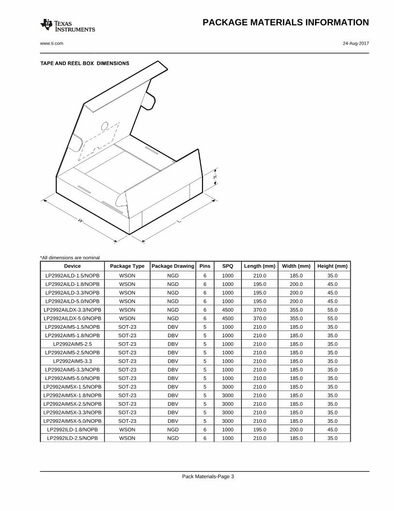
*All dimensions are nominal
Device Package Type Package Drawing Pins SPQ Length (mm) Width (mm) Height (mm)
LP2992AILD-1.5/NOPB WSON NGD 6 1000 210.0 185.0 35.0
LP2992AILD-1.8/NOPB WSON NGD 6 1000 195.0 200.0 45.0
LP2992AILD-3.3/NOPB WSON NGD 6 1000 195.0 200.0 45.0
LP2992AILD-5.0/NOPB WSON NGD 6 1000 195.0 200.0 45.0
LP2992AILDX-3.3/NOPB WSON NGD 6 4500 370.0 355.0 55.0
LP2992AILDX-5.0/NOPB WSON NGD 6 4500 370.0 355.0 55.0
LP2992AIM5-1.5/NOPB SOT-23 DBV 5 1000 210.0 185.0 35.0
LP2992AIM5-1.8/NOPB SOT-23 DBV 5 1000 210.0 185.0 35.0
LP2992AIM5-2.5 SOT-23 DBV 5 1000 210.0 185.0 35.0
LP2992AIM5-2.5/NOPB SOT-23 DBV 5 1000 210.0 185.0 35.0
LP2992AIM5-3.3 SOT-23 DBV 5 1000 210.0 185.0 35.0
LP2992AIM5-3.3/NOPB SOT-23 DBV 5 1000 210.0 185.0 35.0
LP2992AIM5-5.0/NOPB SOT-23 DBV 5 1000 210.0 185.0 35.0
LP2992AIM5X-1.5/NOPB SOT-23 DBV 5 3000 210.0 185.0 35.0
LP2992AIM5X-1.8/NOPB SOT-23 DBV 5 3000 210.0 185.0 35.0
LP2992AIM5X-2.5/NOPB SOT-23 DBV 5 3000 210.0 185.0 35.0
LP2992AIM5X-3.3/NOPB SOT-23 DBV 5 3000 210.0 185.0 35.0
LP2992AIM5X-5.0/NOPB SOT-23 DBV 5 3000 210.0 185.0 35.0
LP2992ILD-1.8/NOPB WSON NGD 6 1000 195.0 200.0 45.0
LP2992ILD-2.5/NOPB WSON NGD 6 1000 210.0 185.0 35.0
PACKAGE MATERIALS INFORMATION
www.ti.com 24-Aug-2017
Pack Materials-Page 3

Device Package Type Package Drawing Pins SPQ Length (mm) Width (mm) Height (mm)
LP2992ILD-3.3/NOPB WSON NGD 6 1000 195.0 200.0 45.0
LP2992ILD-5.0/NOPB WSON NGD 6 1000 195.0 200.0 45.0
LP2992ILDX-1.5/NOPB WSON NGD 6 4500 370.0 355.0 55.0
LP2992ILDX-3.3/NOPB WSON NGD 6 4500 370.0 355.0 55.0
LP2992ILDX-5.0/NOPB WSON NGD 6 4500 367.0 367.0 35.0
LP2992IM5-1.5/NOPB SOT-23 DBV 5 1000 210.0 185.0 35.0
LP2992IM5-1.8 SOT-23 DBV 5 1000 210.0 185.0 35.0
LP2992IM5-1.8/NOPB SOT-23 DBV 5 1000 210.0 185.0 35.0
LP2992IM5-2.5 SOT-23 DBV 5 1000 210.0 185.0 35.0
LP2992IM5-2.5/NOPB SOT-23 DBV 5 1000 210.0 185.0 35.0
LP2992IM5-3.0 SOT-23 DBV 5 1000 210.0 185.0 35.0
LP2992IM5-3.0/NOPB SOT-23 DBV 5 1000 210.0 185.0 35.0
LP2992IM5-3.3 SOT-23 DBV 5 1000 210.0 185.0 35.0
LP2992IM5-3.3/NOPB SOT-23 DBV 5 1000 210.0 185.0 35.0
LP2992IM5-5.0/NOPB SOT-23 DBV 5 1000 210.0 185.0 35.0
LP2992IM5X-1.5/NOPB SOT-23 DBV 5 3000 210.0 185.0 35.0
LP2992IM5X-1.8/NOPB SOT-23 DBV 5 3000 210.0 185.0 35.0
LP2992IM5X-2.5/NOPB SOT-23 DBV 5 3000 210.0 185.0 35.0
LP2992IM5X-3.3/NOPB SOT-23 DBV 5 3000 210.0 185.0 35.0
LP2992IM5X-5.0/NOPB SOT-23 DBV 5 3000 210.0 185.0 35.0
PACKAGE MATERIALS INFORMATION
www.ti.com 24-Aug-2017
Pack Materials-Page 4

MECHANICAL DATA
NGD0006A
www.ti.com


www.ti.com
PACKAGE OUTLINE
C
TYP0.220.08
0.25
3.02.6
2X 0.95
1.9
1.45 MAX
TYP0.150.00
5X 0.50.3
TYP0.60.3
TYP80
1.9
A
3.052.75
B1.751.45
(1.1)
SOT-23 - 1.45 mm max heightDBV0005ASMALL OUTLINE TRANSISTOR
4214839/C 04/2017
NOTES: 1. All linear dimensions are in millimeters. Any dimensions in parenthesis are for reference only. Dimensioning and tolerancing per ASME Y14.5M.2. This drawing is subject to change without notice.3. Refernce JEDEC MO-178.
0.2 C A B
1
34
5
2
INDEX AREAPIN 1
GAGE PLANE
SEATING PLANE
0.1 C
SCALE 4.000

www.ti.com
EXAMPLE BOARD LAYOUT
0.07 MAXARROUND
0.07 MINARROUND
5X (1.1)
5X (0.6)
(2.6)
(1.9)
2X (0.95)
(R0.05) TYP
4214839/C 04/2017
SOT-23 - 1.45 mm max heightDBV0005ASMALL OUTLINE TRANSISTOR
NOTES: (continued) 4. Publication IPC-7351 may have alternate designs. 5. Solder mask tolerances between and around signal pads can vary based on board fabrication site.
SYMM
LAND PATTERN EXAMPLEEXPOSED METAL SHOWN
SCALE:15X
PKG
1
3 4
5
2
SOLDER MASKOPENINGMETAL UNDER
SOLDER MASK
SOLDER MASKDEFINED
EXPOSED METAL
METALSOLDER MASKOPENING
NON SOLDER MASKDEFINED
(PREFERRED)
SOLDER MASK DETAILS
EXPOSED METAL

www.ti.com
EXAMPLE STENCIL DESIGN
(2.6)
(1.9)
2X(0.95)
5X (1.1)
5X (0.6)
(R0.05) TYP
SOT-23 - 1.45 mm max heightDBV0005ASMALL OUTLINE TRANSISTOR
4214839/C 04/2017
NOTES: (continued) 6. Laser cutting apertures with trapezoidal walls and rounded corners may offer better paste release. IPC-7525 may have alternate design recommendations. 7. Board assembly site may have different recommendations for stencil design.
SOLDER PASTE EXAMPLEBASED ON 0.125 mm THICK STENCIL
SCALE:15X
SYMM
PKG
1
3 4
5
2

IMPORTANT NOTICE
Texas Instruments Incorporated (TI) reserves the right to make corrections, enhancements, improvements and other changes to itssemiconductor products and services per JESD46, latest issue, and to discontinue any product or service per JESD48, latest issue. Buyersshould obtain the latest relevant information before placing orders and should verify that such information is current and complete.TI’s published terms of sale for semiconductor products (http://www.ti.com/sc/docs/stdterms.htm) apply to the sale of packaged integratedcircuit products that TI has qualified and released to market. Additional terms may apply to the use or sale of other types of TI products andservices.Reproduction of significant portions of TI information in TI data sheets is permissible only if reproduction is without alteration and isaccompanied by all associated warranties, conditions, limitations, and notices. TI is not responsible or liable for such reproduceddocumentation. Information of third parties may be subject to additional restrictions. Resale of TI products or services with statementsdifferent from or beyond the parameters stated by TI for that product or service voids all express and any implied warranties for theassociated TI product or service and is an unfair and deceptive business practice. TI is not responsible or liable for any such statements.Buyers and others who are developing systems that incorporate TI products (collectively, “Designers”) understand and agree that Designersremain responsible for using their independent analysis, evaluation and judgment in designing their applications and that Designers havefull and exclusive responsibility to assure the safety of Designers' applications and compliance of their applications (and of all TI productsused in or for Designers’ applications) with all applicable regulations, laws and other applicable requirements. Designer represents that, withrespect to their applications, Designer has all the necessary expertise to create and implement safeguards that (1) anticipate dangerousconsequences of failures, (2) monitor failures and their consequences, and (3) lessen the likelihood of failures that might cause harm andtake appropriate actions. Designer agrees that prior to using or distributing any applications that include TI products, Designer willthoroughly test such applications and the functionality of such TI products as used in such applications.TI’s provision of technical, application or other design advice, quality characterization, reliability data or other services or information,including, but not limited to, reference designs and materials relating to evaluation modules, (collectively, “TI Resources”) are intended toassist designers who are developing applications that incorporate TI products; by downloading, accessing or using TI Resources in anyway, Designer (individually or, if Designer is acting on behalf of a company, Designer’s company) agrees to use any particular TI Resourcesolely for this purpose and subject to the terms of this Notice.TI’s provision of TI Resources does not expand or otherwise alter TI’s applicable published warranties or warranty disclaimers for TIproducts, and no additional obligations or liabilities arise from TI providing such TI Resources. TI reserves the right to make corrections,enhancements, improvements and other changes to its TI Resources. TI has not conducted any testing other than that specificallydescribed in the published documentation for a particular TI Resource.Designer is authorized to use, copy and modify any individual TI Resource only in connection with the development of applications thatinclude the TI product(s) identified in such TI Resource. NO OTHER LICENSE, EXPRESS OR IMPLIED, BY ESTOPPEL OR OTHERWISETO ANY OTHER TI INTELLECTUAL PROPERTY RIGHT, AND NO LICENSE TO ANY TECHNOLOGY OR INTELLECTUAL PROPERTYRIGHT OF TI OR ANY THIRD PARTY IS GRANTED HEREIN, including but not limited to any patent right, copyright, mask work right, orother intellectual property right relating to any combination, machine, or process in which TI products or services are used. Informationregarding or referencing third-party products or services does not constitute a license to use such products or services, or a warranty orendorsement thereof. Use of TI Resources may require a license from a third party under the patents or other intellectual property of thethird party, or a license from TI under the patents or other intellectual property of TI.TI RESOURCES ARE PROVIDED “AS IS” AND WITH ALL FAULTS. TI DISCLAIMS ALL OTHER WARRANTIES ORREPRESENTATIONS, EXPRESS OR IMPLIED, REGARDING RESOURCES OR USE THEREOF, INCLUDING BUT NOT LIMITED TOACCURACY OR COMPLETENESS, TITLE, ANY EPIDEMIC FAILURE WARRANTY AND ANY IMPLIED WARRANTIES OFMERCHANTABILITY, FITNESS FOR A PARTICULAR PURPOSE, AND NON-INFRINGEMENT OF ANY THIRD PARTY INTELLECTUALPROPERTY RIGHTS. TI SHALL NOT BE LIABLE FOR AND SHALL NOT DEFEND OR INDEMNIFY DESIGNER AGAINST ANY CLAIM,INCLUDING BUT NOT LIMITED TO ANY INFRINGEMENT CLAIM THAT RELATES TO OR IS BASED ON ANY COMBINATION OFPRODUCTS EVEN IF DESCRIBED IN TI RESOURCES OR OTHERWISE. IN NO EVENT SHALL TI BE LIABLE FOR ANY ACTUAL,DIRECT, SPECIAL, COLLATERAL, INDIRECT, PUNITIVE, INCIDENTAL, CONSEQUENTIAL OR EXEMPLARY DAMAGES INCONNECTION WITH OR ARISING OUT OF TI RESOURCES OR USE THEREOF, AND REGARDLESS OF WHETHER TI HAS BEENADVISED OF THE POSSIBILITY OF SUCH DAMAGES.Unless TI has explicitly designated an individual product as meeting the requirements of a particular industry standard (e.g., ISO/TS 16949and ISO 26262), TI is not responsible for any failure to meet such industry standard requirements.Where TI specifically promotes products as facilitating functional safety or as compliant with industry functional safety standards, suchproducts are intended to help enable customers to design and create their own applications that meet applicable functional safety standardsand requirements. Using products in an application does not by itself establish any safety features in the application. Designers mustensure compliance with safety-related requirements and standards applicable to their applications. Designer may not use any TI products inlife-critical medical equipment unless authorized officers of the parties have executed a special contract specifically governing such use.Life-critical medical equipment is medical equipment where failure of such equipment would cause serious bodily injury or death (e.g., lifesupport, pacemakers, defibrillators, heart pumps, neurostimulators, and implantables). Such equipment includes, without limitation, allmedical devices identified by the U.S. Food and Drug Administration as Class III devices and equivalent classifications outside the U.S.TI may expressly designate certain products as completing a particular qualification (e.g., Q100, Military Grade, or Enhanced Product).Designers agree that it has the necessary expertise to select the product with the appropriate qualification designation for their applicationsand that proper product selection is at Designers’ own risk. Designers are solely responsible for compliance with all legal and regulatoryrequirements in connection with such selection.Designer will fully indemnify TI and its representatives against any damages, costs, losses, and/or liabilities arising out of Designer’s non-compliance with the terms and provisions of this Notice.
Mailing Address: Texas Instruments, Post Office Box 655303, Dallas, Texas 75265Copyright © 2018, Texas Instruments Incorporated