Section 37. Charge Time Measurement Unit (CTMU)
24
© 2011-2012 Microchip Technology Inc. DS61167B-page 37-1 Charge Time Measurement Unit (CTMU) 37 Section 37. Charge Time Measurement Unit (CTMU) HIGHLIGHTS This section of the manual contains the following major topics: 37.1 Introduction .................................................................................................................. 37-2 37.2 Registers ...................................................................................................................... 37-3 37.3 CTMU Operation .......................................................................................................... 37-6 37.4 CTMU Module Initialization .......................................................................................... 37-8 37.5 Calibrating the CTMU Module...................................................................................... 37-9 37.6 Measuring Capacitance with the CTMU..................................................................... 37-15 37.7 Measuring Time with the CTMU Module .................................................................... 37-18 37.8 Creating a Delay with the CTMU Module................................................................... 37-18 37.9 Measuring On-Chip Temperature with the CTMU ...................................................... 37-19 37.10 Operation During Sleep/Idle Modes ........................................................................... 37-20 37.11 Effects of a Reset on CTMU ...................................................................................... 37-20 37.12 Related Application Notes.......................................................................................... 37-21 37.13 Revision History ......................................................................................................... 37-22
Transcript of Section 37. Charge Time Measurement Unit (CTMU)

Section 37. Charge Time Measurement Unit (CTMU)
Charge Tim
e M
easurement U
nit (C
TMU
)
37
HIGHLIGHTSThis section of the manual contains the following major topics:
37.1 Introduction .................................................................................................................. 37-237.2 Registers...................................................................................................................... 37-337.3 CTMU Operation.......................................................................................................... 37-637.4 CTMU Module Initialization .......................................................................................... 37-837.5 Calibrating the CTMU Module...................................................................................... 37-937.6 Measuring Capacitance with the CTMU..................................................................... 37-1537.7 Measuring Time with the CTMU Module.................................................................... 37-1837.8 Creating a Delay with the CTMU Module................................................................... 37-1837.9 Measuring On-Chip Temperature with the CTMU...................................................... 37-1937.10 Operation During Sleep/Idle Modes........................................................................... 37-2037.11 Effects of a Reset on CTMU ...................................................................................... 37-2037.12 Related Application Notes.......................................................................................... 37-2137.13 Revision History ......................................................................................................... 37-22
© 2011-2012 Microchip Technology Inc. DS61167B-page 37-1

PIC32 Family Reference Manual
37.1 INTRODUCTIONThe Charge Time Measurement Unit (CTMU) is a flexible analog module that has a configurablecurrent source with a digital configuration circuit built around it. The CTMU can be used fordifferential time measurement between pulse sources and can be used for generating an asyn-chronous pulse. By working with other on-chip analog modules, the CTMU can be used for highresolution time measurement, measure capacitance, measure relative changes in capacitanceor generate output pulses with a specific time delay. The CTMU is ideal for interfacing withcapacitive-based sensors.The module includes the following key features:
• Up to 32 channels available for capacitive or time measurement input• On-chip precision current source• 16-edge input trigger sources• Selection of edge or level-sensitive inputs• Polarity control for each edge source• Control of edge sequence• Control of response to edges• High precision time measurement• Time delay of external or internal signal asynchronous to system clock• Integrated temperature sensing diode• Control of current source during auto-sampling• Four current source ranges• Time measurement resolution of one nanosecond
The CTMU works in conjunction with the Analog-to-Digital Converter (ADC) to provide up to 32channels for time or charge measurement, depending on the specific device and the number ofADC channels available. When configured for time delay, the CTMU is connected to one of theanalog comparators. The level-sensitive input edge sources can be selected from four sources:two external inputs, Timer1 or Output Compare Module 1. For information on available inputsources, refer to the specific device data sheet. A block diagram of the CTMU is shown in Figure 37-1.
Figure 37-1: CTMU Block Diagram
Note: This family reference manual section is meant to serve as a complement to devicedata sheets. Depending on the device variant, this manual section may not apply toall PIC32 devices.Please consult the note at the beginning of the “Charge Time Measurement Unit(CTMU)” chapter in the current device data sheet to check whether this documentsupports the device you are using.Device data sheets and family reference manual sections are available fordownload from the Microchip Worldwide Web site at: http://www.microchip.com
CTED16
CTED1
Current Source
EdgeControlLogic
PulseGenerator
ADC Comparator 2Input
OC1
CurrentControl
ITRIM<5:0>IRNG<1:0>
CTMUCON
CTMUControlLogic
EDGENEDGSEQENEDG1SELxEDG1POLEDG2SELxEDG2POL EDG1STAT
EDG2STAT
TGENIDISSENCTTRIG
ADC Trigger
CTPLS
Comparator 2 Output
EDG1MODEDG2MOD
...
Timer1
DS61167B-page 37-2 © 2011-2012 Microchip Technology Inc.

Section 37. Charge Time Measurement Unit (CTMU)C
harge Time
Measurem
ent Unit
(CTM
U)
37
37.2 REGISTERSThe CTMUCON register contains control bits for configuring the CTMU module edge sourceselection, edge source polarity selection, edge sequencing, ADC trigger, analog circuit capacitordischarge and enables. In addition, this register has bits for selecting the current source rangeand current source trim.
Table 37-1 summarizes the CTMU-related register. A detailed description of the register followsthe summary.
Table 37-1: CTMU SFR Summary(1)
Name BitRange
Bit31/23/15/7
Bit30/22/14/6
Bit29/21/13/5
Bit28/20/12/4
Bit27/19/11/3
Bit26/18/10/2
Bit25/17/9/1
Bit24/16/8/0
CTMUCON 31:24 EDG1MOD EDG1POL EDG1SEL<3:0> EDG2STAT EDG1STAT23:16 EDG2MOD EDG2POL EDG2SEL<3:0> — —15:8 ON — CTMUSIDL TGEN EDGEN EDGSEQEN IDISSEN CTTRIG7:0 ITRIM<5:0> IRNG<1:0>
Legend: — = unimplemented, read as ‘0’. Address offset values are shown in hexadecimal.Note 1: Not all registers have associated SET, CLR, and INV registers. Refer to the specific device data sheet for details.
© 2011-2012 Microchip Technology Inc. DS61167B-page 37-3
PIC32 Family Reference Manual
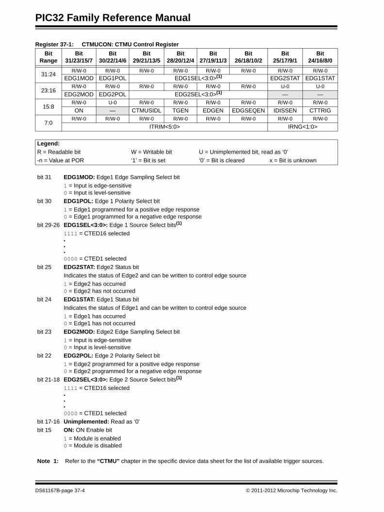
Register 37-1: CTMUCON: CTMU Control RegisterBit
RangeBit
31/23/15/7Bit
30/22/14/6Bit
29/21/13/5Bit
28/20/12/4Bit
27/19/11/3Bit
26/18/10/2Bit
25/17/9/1Bit
24/16/8/0
31:24 R/W-0 R/W-0 R/W-0 R/W-0 R/W-0 R/W-0 R/W-0 R/W-0EDG1MOD EDG1POL EDG1SEL<3:0>(1) EDG2STAT EDG1STAT
23:16R/W-0 R/W-0 R/W-0 R/W-0 R/W-0 R/W-0 U-0 U-0
EDG2MOD EDG2POL EDG2SEL<3:0>(1) — —
15:8R/W-0 U-0 R/W-0 R/W-0 R/W-0 R/W-0 R/W-0 R/W-0ON — CTMUSIDL TGEN EDGEN EDGSEQEN IDISSEN CTTRIG
7:0R/W-0 R/W-0 R/W-0 R/W-0 R/W-0 R/W-0 R/W-0 R/W-0
ITRIM<5:0> IRNG<1:0>
Legend:R = Readable bit W = Writable bit U = Unimplemented bit, read as ‘0’-n = Value at POR ‘1’ = Bit is set ‘0’ = Bit is cleared x = Bit is unknown
bit 31 EDG1MOD: Edge1 Edge Sampling Select bit1 = Input is edge-sensitive0 = Input is level-sensitive
bit 30 EDG1POL: Edge 1 Polarity Select bit1 = Edge1 programmed for a positive edge response0 = Edge1 programmed for a negative edge response
bit 29-26 EDG1SEL<3:0>: Edge 1 Source Select bits(1)
1111 = CTED16 selected•••0000 = CTED1 selected
bit 25 EDG2STAT: Edge2 Status bit Indicates the status of Edge2 and can be written to control edge source1 = Edge2 has occurred0 = Edge2 has not occurred
bit 24 EDG1STAT: Edge1 Status bit Indicates the status of Edge1 and can be written to control edge source1 = Edge1 has occurred0 = Edge1 has not occurred
bit 23 EDG2MOD: Edge2 Edge Sampling Select bit1 = Input is edge-sensitive0 = Input is level-sensitive
bit 22 EDG2POL: Edge 2 Polarity Select bit1 = Edge2 programmed for a positive edge response0 = Edge2 programmed for a negative edge response
bit 21-18 EDG2SEL<3:0>: Edge 2 Source Select bits(1)
1111 = CTED16 selected•••0000 = CTED1 selected
bit 17-16 Unimplemented: Read as ‘0’bit 15 ON: ON Enable bit
1 = Module is enabled0 = Module is disabled
Note 1: Refer to the “CTMU” chapter in the specific device data sheet for the list of available trigger sources.
DS61167B-page 37-4 © 2011-2012 Microchip Technology Inc.

Section 37. Charge Time Measurement Unit (CTMU)C
harge Time
Measurem
ent Unit
(CTM
U)
37
bit 14 Unimplemented: Read as ‘0’bit 13 CTMUSIDL: Stop in Idle Mode bit
1 = Discontinue module operation when device enters Idle mode0 = Continue module operation in Idle mode
bit 12 TGEN: Time Generation Enable bit1 = Enables edge delay generation0 = Disables edge delay generation
bit 11 EDGEN: Edge Enable bit1 = Edges are not blocked0 = Edges are blocked
bit 10 EDGSEQEN: Edge Sequence Enable bit1 = Edge1 must occur before Edge2 can occur0 = No edge sequence is needed
bit 9 IDISSEN: Current Discharge Enable bit 1 = Analog current source output is grounded0 = Analog current source output is not grounded
bit 8 CTTRIG: Trigger Control bit 1 = Trigger output is enabled0 = Trigger output is disabled
bit 7-2 ITRIM<5:0>: Current Source Trim bits111111 = Minimum negative change from nominal current•••100010 100001 = Maximum negative change from nominal current011111 = Maximum positive change from nominal current011110 •••000001 = Minimum positive change from nominal current000000 = Nominal current output specified by IRNG<1:0>
bit 1-0 IRNG<1:0>: Current Range Select bits11 = 100 times base current10 = 10 times base current01 = Base current level (0.55 μA nominal)00 = 1000 times base current
Register 37-1: CTMUCON: CTMU Control Register (Continued)
Note 1: Refer to the “CTMU” chapter in the specific device data sheet for the list of available trigger sources.
© 2011-2012 Microchip Technology Inc. DS61167B-page 37-5

PIC32 Family Reference Manual
37.3 CTMU OPERATIONThe CTMU works by using a constant current source to charge a circuit. The type of circuitdepends on the type of measurement being made. In the case of capacitance measurement, thecurrent is fixed and the amount of time the current is applied to the circuit is fixed. The amountof voltage read by the ADC is then a measurement of the capacitance of the circuit. In the caseof time measurement, the current, as well as the capacitance of the circuit, is fixed and chargetime varies. In this case, the voltage read by the ADC is then representative of the amount of timeelapsed from the time the current source starts and stops charging the circuit.
If the CTMU is being used as a time delay, both capacitance and current source are fixed, as wellas the voltage supplied to the comparator circuit. The delay of a signal is determined by theamount of time taken for the voltage to charge to the comparator threshold voltage.
37.3.1 Theory of OperationThe operation of the CTMU is based on the equation for charge, as shown in Equation 37-1.
Equation 37-1:
More simply, the amount of charge measured in coulombs in a circuit is defined as current inamperes (I) multiplied by the amount of time in seconds that the current flows (t). Charge is alsodefined as the capacitance in farads (C) multiplied by the voltage of the circuit (V), as shown inEquation 37-2.
Equation 37-2:
The CTMU module provides a constant, known current source. The ADC is used to measure (V)in the equation, leaving two unknowns: capacitance (C) and time (t). Equation 37-2 can be usedto calculate capacitance or time, by either the relationship shown in Equation 37-3 and using theknown fixed capacitance of the circuit, or by Equation 37-4 using a fixed time that the currentsource is applied to the circuit.
Equation 37-3:
Equation 37-4:
I C dVdt-------⋅=
I t⋅ C V⋅=
t C V⋅( )I
-----------------=
C I t⋅( )V
-------------=
DS61167B-page 37-6 © 2011-2012 Microchip Technology Inc.
Section 37. Charge Time Measurement Unit (CTMU)C
harge Time
Measurem
ent Unit
(CTM
U)
37
37.3.2 Current SourceAt the heart of the CTMU is a precision current source, designed to provide a constant referencefor measurements. The level of current is user-selectable across four ranges, or a total of twoorders of magnitude, with the ability to trim the output in ±2% increments (nominal). The currentrange is selected by the IRNG<1:0> bits (CTMUCON<1:0>) with a value of ‘01’ representing thelowest range. Current trim is provided by the ITRIM<5:0> bits (CTMUCON<7:2>). These six bits allow trimmingof the current source in steps of approximately 2% per step. Note that half of the range adjuststhe current source positively and the other half reduces the current source. A value of ‘000000’is the neutral position (no change). A value of ‘100001’ (see Note 1) is the maximum negativeadjustment (approximately -62%) and ‘011111’ (see Note 2) is the maximum positiveadjustment (approximately +62%).
37.3.3 Edge Selection and ControlCTMU measurements are controlled by edge events occurring on the module’s two inputchannels. Each channel, referred as Edge 1 and Edge 2, can be configured to receive inputpulses from one of the sixteen edge input pins. The inputs are selected using theEDG1SEL<3:0> and EDG2SEL<3:0> bit pairs (CTMUCON<29:26> and CTMUCON<21:18>).
In addition to source, each channel can be configured for event polarity using the EDG1POL andEDG2POL bits (CTMUCON<30>and CTMUCON<22>). The input channels can also be filteredfor an edge event sequence (Edge 1 occurring before Edge 2) by setting the EDGSEQEN bit(CTMUCON<10>).
37.3.4 Edge StatusThe CTMUCON register also contains two status bits: EDG1STAT (CTMUCON<24>) andEDG2STAT (CTMUCON<25>). Their primary function is to show if an edge response hasoccurred on the corresponding channel. The CTMU automatically sets a particular bit when anedge response is detected on its channel. The level-sensitive or edge-sensitive nature of theinput channels means that the status bits are set immediately if the channel’s configurationchanges and remains in the new state.
The CTMU module uses the edge status bits to control the current source output to external ana-log modules (such as the ADC). Current is supplied to external modules only when one (but notboth) of the status bits is set and shuts current off when both bits are either set or cleared. Thisallows the CTMU to measure current only during the interval between edges. After both thestatus bits are set, it is necessary to clear them before another measurement is taken. Both thebits should be cleared simultaneously, if possible, to avoid re-enabling the CTMU current source.
In addition to being set by the CTMU hardware, the edge status bits can also be set by software.This allows the user’s application to manually enable or disable the current source. Setting eitherone (but not both) of the bits enables the current source. Setting or clearing both bits at oncedisables the source.
37.3.5 InterruptsThe CTMU sets its interrupt flag (CTMUIF) whenever the current source is enabled and thendisabled. If edge sequencing is not enabled (i.e., Edge 1 must occur before Edge 2), it isnecessary to monitor the edge status bits and determine which edge occurred last and causedthe interrupt.
Note 1: The value '100001' = -31 & 0x3F → iTRIM = -31 * Delta I, approximately -62% ofnominal.
2: The value '011111' = +31 & 0x3F → iTRIM = +31 * Delta I, approximately +62% ofnominal.
© 2011-2012 Microchip Technology Inc. DS61167B-page 37-7
PIC32 Family Reference Manual
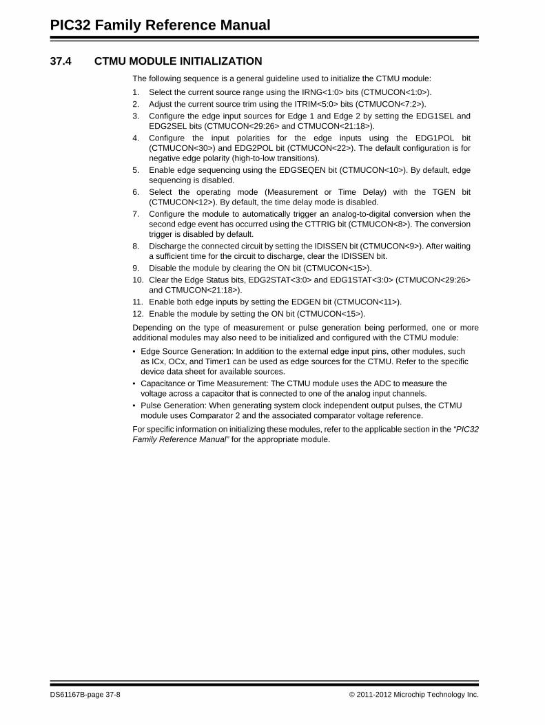
37.4 CTMU MODULE INITIALIZATIONThe following sequence is a general guideline used to initialize the CTMU module:
1. Select the current source range using the IRNG<1:0> bits (CTMUCON<1:0>).2. Adjust the current source trim using the ITRIM<5:0> bits (CTMUCON<7:2>). 3. Configure the edge input sources for Edge 1 and Edge 2 by setting the EDG1SEL and
EDG2SEL bits (CTMUCON<29:26> and CTMUCON<21:18>).4. Configure the input polarities for the edge inputs using the EDG1POL bit
(CTMUCON<30>) and EDG2POL bit (CTMUCON<22>). The default configuration is fornegative edge polarity (high-to-low transitions).
5. Enable edge sequencing using the EDGSEQEN bit (CTMUCON<10>). By default, edgesequencing is disabled.
6. Select the operating mode (Measurement or Time Delay) with the TGEN bit(CTMUCON<12>). By default, the time delay mode is disabled.
7. Configure the module to automatically trigger an analog-to-digital conversion when thesecond edge event has occurred using the CTTRIG bit (CTMUCON<8>). The conversiontrigger is disabled by default.
8. Discharge the connected circuit by setting the IDISSEN bit (CTMUCON<9>). After waitinga sufficient time for the circuit to discharge, clear the IDISSEN bit.
9. Disable the module by clearing the ON bit (CTMUCON<15>).10. Clear the Edge Status bits, EDG2STAT<3:0> and EDG1STAT<3:0> (CTMUCON<29:26>
and CTMUCON<21:18>).11. Enable both edge inputs by setting the EDGEN bit (CTMUCON<11>).12. Enable the module by setting the ON bit (CTMUCON<15>).
Depending on the type of measurement or pulse generation being performed, one or moreadditional modules may also need to be initialized and configured with the CTMU module:
• Edge Source Generation: In addition to the external edge input pins, other modules, such as ICx, OCx, and Timer1 can be used as edge sources for the CTMU. Refer to the specific device data sheet for available sources.
• Capacitance or Time Measurement: The CTMU module uses the ADC to measure the voltage across a capacitor that is connected to one of the analog input channels.
• Pulse Generation: When generating system clock independent output pulses, the CTMU module uses Comparator 2 and the associated comparator voltage reference.
For specific information on initializing these modules, refer to the applicable section in the “PIC32Family Reference Manual” for the appropriate module.
DS61167B-page 37-8 © 2011-2012 Microchip Technology Inc.

Section 37. Charge Time Measurement Unit (CTMU)C
harge Time
Measurem
ent Unit
(CTM
U)
37
37.5 CALIBRATING THE CTMU MODULEThe CTMU requires calibration for precise measurements of capacitance and time, as well as foraccurate time delay. If the application requires only measurement of a relative change in capac-itance or time, calibration is usually not necessary. An example of this type of application wouldinclude a capacitive touch switch, in which the touch circuit has a baseline capacitance and theadded capacitance of the human body changes the overall capacitance of a circuit.
If actual capacitance or time measurement is required, two hardware calibrations must takeplace: the current source needs calibration to set it to a precise current, and the circuit beingmeasured needs calibration to measure and/or nullify all other capacitance other than that to bemeasured.
37.5.1 Current Source CalibrationThe current source on-board the CTMU module has a range of ±62% nominal for each of fourcurrent ranges. Therefore, for precise measurements, it is possible to measure and adjust thiscurrent source by placing a high precision resistor, RCAL, onto a special analog channel. Anexample circuit is shown in Figure 37-2. The current source measurement is performed using thefollowing steps:
1. Initialize the ADC.2. Initialize the CTMU by configuring the module for Pulse Generation (TGEN = 1) mode.3. Enable the current source by setting the EDG1STAT bit (CTMUCON<24>).4. Issue settling time delay.5. Perform analog-to-digital conversion.6. Calculate the current source current using I = V/RCAL, where RCAL is a high precision
resistance and V is measured by performing an analog-to-digital conversion.
The CTMU current source may be trimmed with the trim bits in the CTMUCON register using aniterative process to get an exact desired current. Alternatively, the nominal value without adjust-ment may be used. It may be stored by the software for use in all subsequent capacitive or timemeasurements.
Figure 37-2 shows the external connections for current source calibration, as well as the relationshipof the different analog modules required.
CTMU charge pump calibration should be done only on the special pin that connects to the Com-parator module associated with the CTMU. Use of any other ANx pin will add around 2.5 kΩ of seriesresistance to the measurement from the analog multiplexer in front of the ADC. This effect can beignored only for the smallest current settings. For larger current settings, the uncertainty in the extraseries resistance overwhelms the overall resistance accuracy from the calibration resistor.
To calculate the value for RCAL, the nominal current must be chosen and then the resistance canbe calculated. For example, if the ADC reference voltage is 3.3V, use 70% of full scale, or 2.31Vas the desired approximate voltage to be read by the ADC. If the range of the CTMU currentsource is selected to be 0.55 μA, the required resistor value is calculated asRCAL = 2.31V/0.55 µA, for a value of 4.2 MΩ. Similarly, if the current source is chosen to be5.5 µA, RCAL would be 420,000Ω and 42,000Ω if the current source is set to 55 µA.
© 2011-2012 Microchip Technology Inc. DS61167B-page 37-9
PIC32 Family Reference Manual
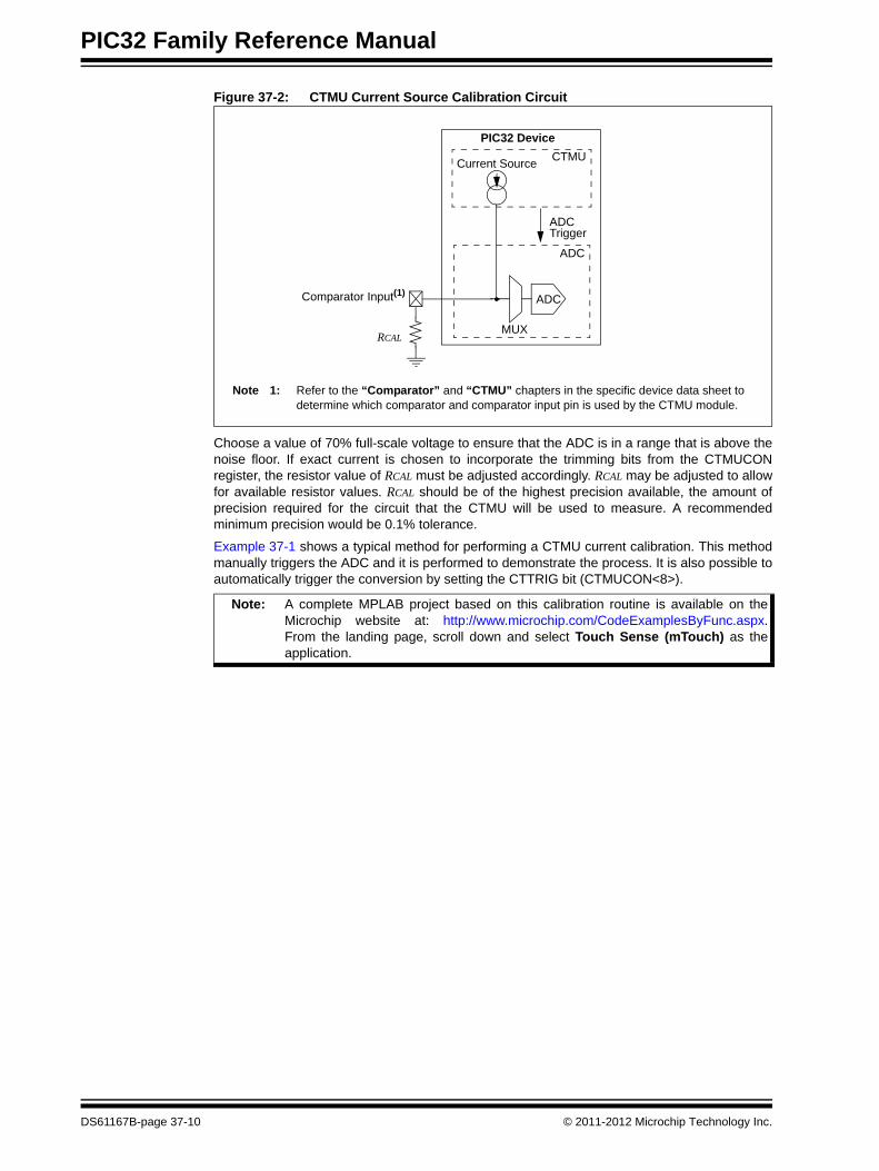
Figure 37-2: CTMU Current Source Calibration Circuit
Choose a value of 70% full-scale voltage to ensure that the ADC is in a range that is above thenoise floor. If exact current is chosen to incorporate the trimming bits from the CTMUCONregister, the resistor value of RCAL must be adjusted accordingly. RCAL may be adjusted to allowfor available resistor values. RCAL should be of the highest precision available, the amount ofprecision required for the circuit that the CTMU will be used to measure. A recommendedminimum precision would be 0.1% tolerance.
Example 37-1 shows a typical method for performing a CTMU current calibration. This methodmanually triggers the ADC and it is performed to demonstrate the process. It is also possible toautomatically trigger the conversion by setting the CTTRIG bit (CTMUCON<8>).
Note: A complete MPLAB project based on this calibration routine is available on theMicrochip website at: http://www.microchip.com/CodeExamplesByFunc.aspx.From the landing page, scroll down and select Touch Sense (mTouch) as theapplication.
PIC32 Device
ADC
CTMU
Comparator Input(1)
RCAL
Current Source
ADCTrigger
ADC
MUX
Note 1: Refer to the “Comparator” and “CTMU” chapters in the specific device data sheet to determine which comparator and comparator input pin is used by the CTMU module.
DS61167B-page 37-10 © 2011-2012 Microchip Technology Inc.

Section 37. Charge Time Measurement Unit (CTMU)C
harge Time
Measurem
ent Unit
(CTM
U)
37
Example 37-1: Current Calibration Routine// Device setup - TO DO: Set up device with #pragma's
int main(void) unsigned long int ADC_Sum; // For averaging multiple ADC measurements unsigned short int iAvg, // Averaging index Naverages = 1024, // Number of averages < 2^22 (22=32-10 bits of ADC) Log2Naverages = 10; // Right shift equal to 1/Naverages short int iTrim; // Current trim index unsigned short int VmeasADC, VavgADC; // Measured Voltages, 65536 = Full Scale
// TO DO: Disable JTAG and enable multivector interrupt table// Set up UART2 for transmission of button data// TO DO: Set up pins
// CTMU Setup CTMUCONbits.TGEN = 1; // Enable direct output to C2INB/AN2 pin CTMUCONbits.IRNG = 0x3; // Current Range
// Turn on CTMU after setting current trim below
// ADC Setup AD1CON2 = 0x0; // VR+ = AVDD, V- = AVSS, Don't scan, MUX A only
// ADC clock derived from peripheral buss clock // Tadc = 4 * Tpbus = 4 * 25 ns = 100 ns > 65 ns required // Tadc = 2*(1+1)*Tpbus // Tadc = 2*(AD1CON3<7:0>+1)*Tpbus AD1CON3 = 1;
AD1CSSL = 0x0; // No channels scanned AD1CHSbits.CH0SA = 2; // Select channel AN2 (PG1D/AN2/C2INB)
ANSELA = 0x0000; // No ADC pins ANSELB = 1<<0; // RB0: for AN2/C2INB, which is connected to Rcal ANSELC = 0x0000; // No ADC pins
IEC0bits.AD1IE = 0; // Disable ADC interruptsAD1CON1bits.ON = 1; // Turn on ADC
// Sweep over all possible current trim values for ( iTrim = -31; iTrim < 32; iTrim++ ) CTMUCONbits.ITRIM = iTrim & 0x3F; // Set current trim value CTMUCONbits.ON = 1; // Turn on CTMU // TO DO: Add delay of 1 ms
ADC_Sum = 0; for ( iAvg = 0; iAvg < Naverages; iAvg++ ) CTMUCONCLR = 0x03000000; // Clear Status bits at same time AD1CON1bits.SAMP = 1; // Manual sampling start CTMUCONbits.IDISSEN = 1; // Ground charge pump
// TO DO: Add delay of 500 us;CTMUCONbits.IDISSEN = 0; // End drain of circuit
LATASET = 1<<8; // Turn on RA8
CTMUCONbits.EDG1STAT = 1; // Begin charging the circuit LATASET = 1<<7; // Turn on RA7
// TO DO: Wait 25 usAD1CON1bits.SAMP = 0; // Begin analog-to-digital conversionCTMUCONbits.EDG2STAT = 1; // Stop charging circuitwhile (!AD1CON1bits.DONE) // Wait for ADC conversion
// Do Nothing AD1CON1bits.DONE = 0; // ADC conversion done, clear flag VmeasADC = ADC1BUF0; // Get the value from the ADC ADC_Sum += VmeasADC; // Update averaging sum
//end for ( iAvg = 0; iAvg < Naverages; iAvg++ ) CTMUCONbits.ON = 0; // Turn off CTMU
VavgADC = ADC_Sum >> (Log2Naverages-6); // Full scale = 2^10<<6 = 65536
// TO DO: Transmit iTrim and VavgADC using UART
// end for ( iTrim = -31; iTrim < 32; iTrim++ )
// end main()
© 2011-2012 Microchip Technology Inc. DS61167B-page 37-11
PIC32 Family Reference Manual
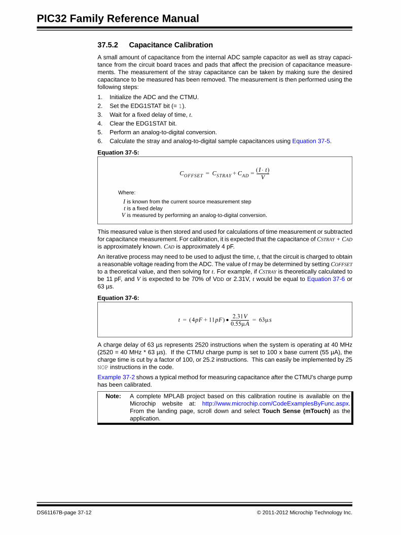
37.5.2 Capacitance CalibrationA small amount of capacitance from the internal ADC sample capacitor as well as stray capaci-tance from the circuit board traces and pads that affect the precision of capacitance measure-ments. The measurement of the stray capacitance can be taken by making sure the desiredcapacitance to be measured has been removed. The measurement is then performed using thefollowing steps:
1. Initialize the ADC and the CTMU.2. Set the EDG1STAT bit (= 1).3. Wait for a fixed delay of time, t.4. Clear the EDG1STAT bit.5. Perform an analog-to-digital conversion.6. Calculate the stray and analog-to-digital sample capacitances using Equation 37-5.
Equation 37-5:
This measured value is then stored and used for calculations of time measurement or subtractedfor capacitance measurement. For calibration, it is expected that the capacitance of CSTRAY + CADis approximately known. CAD is approximately 4 pF.
An iterative process may need to be used to adjust the time, t, that the circuit is charged to obtaina reasonable voltage reading from the ADC. The value of t may be determined by setting COFFSETto a theoretical value, and then solving for t. For example, if CSTRAY is theoretically calculated tobe 11 pF, and V is expected to be 70% of VDD or 2.31V, t would be equal to Equation 37-6 or63 µs.
Equation 37-6:
A charge delay of 63 µs represents 2520 instructions when the system is operating at 40 MHz(2520 = 40 MHz * 63 µs). If the CTMU charge pump is set to 100 x base current (55 µA), thecharge time is cut by a factor of 100, or 25.2 instructions. This can easily be implemented by 25NOP instructions in the code.
Example 37-2 shows a typical method for measuring capacitance after the CTMU's charge pumphas been calibrated.
Note: A complete MPLAB project based on this calibration routine is available on theMicrochip website at: http://www.microchip.com/CodeExamplesByFunc.aspx.From the landing page, scroll down and select Touch Sense (mTouch) as theapplication.
COFFSET CSTRAY CADI t⋅( )V-------------=+=
Where:
I is known from the current source measurement step t is a fixed delay
V is measured by performing an analog-to-digital conversion.
t 4pF 11pF+( ) 2.31V0.55μA------------------• 63μs==
DS61167B-page 37-12 © 2011-2012 Microchip Technology Inc.

Section 37. Charge Time Measurement Unit (CTMU)C
harge Time
Measurem
ent Unit
(CTM
U)
37
Example 37-2: Capacitance Calibration Routine// Device setup - TO DO: Set up device with #pragma's
int main(void) unsigned long int ADC_Sum; // For averaging multiple ADC measurements unsigned short int iAvg, // Averaging index Naverages = 1024, // Number of averages < 2^22 (22=32-10 bits of ADC) Log2Naverages = 10; // Right shift equal to 1/Naverages short int iTrim; // Current trim index unsigned short int VmeasADC, VavgADC; // Measured Voltages, 65536 = Full Scale
// TO DO: Disable JTAG and enable multivector interrupt table// Set up UART2 for transmission of button data.// TO DO: Set up pins
// CTMU Setup CTMUCONbits.TGEN = 1; // Enable direct output to C2INB/AN2 pin CTMUCONbits.IRNG = PLIB_CTMU_CurrentRange_100xBase; //Current Range: 100 x 0.55 = 55 uA
// ADC Setup AD1CON2 = 0x0; // VR+ = AVDD, V- = AVSS, Don't scan, MUX A only
// ADC clock derived from peripheral buss clock // Tadc = 4 * Tpbus = 4 * 25 ns = 100 ns > 65 ns required // Tadc = 2*(1 +1)*Tpbus // Tadc = 2*(AD1CON3<7:0>+1)*Tpbus AD1CON3 = 1;
AD1CSSL = 0x0; // No channels scanned AD1CHSbits.CH0SA = 2; // Select channel AN2
ANSELA = 0x0000; // No ADC pins ANSELB = 1<<0; // RB0: for AN2/C2INB, which is connected to Rcal ANSELC = 0x0000; // No ADC pins
IEC0bits.AD1IE = 0; // Disable ADC interruptsAD1CON1bits.ON = 1; // Turn on ADC
// Sweep over all possible current trim values for ( iTrim = -31; iTrim < 32; iTrim++ ) CTMUCONbits.ITRIM = iTrim & 0x3F; // Set current trim value CTMUCONbits.ON = 1; // Turn on CTMU // TO DO: Wait 1 ms for CTMU start-up
ADC_Sum = 0; for ( iAvg = 0; iAvg < Naverages; iAvg++ )
AD1CON1bits.SAMP = 1; // Manual sampling startCTMUCONbits.IDISSEN = 1; // Ground charge pump// TO DO: Wait 1 ms for groundingCTMUCONbits.IDISSEN = 0; // End drain of circuitCTMUCONbits.EDG1STAT = 1; // Begin charging the circuit// Use Equation 37-6 to solve for charge time with current = 55 uA// Charge time = 0.63 us, or 25.2 NOPs at 40 MHz system clock// TO DO: Wait 25 NOPs
AD1CON1bits.SAMP = 0; // Begin analog-to-digital conversion CTMUCONbits.EDG1STAT = 0; // Stop charging circuit while (!AD1CON1bits.DONE) // Wait for ADC conversion
// Do Nothing AD1CON1bits.DONE = 0; // ADC conversion done, clear flag VmeasADC = ADC1BUF0; // Get the value from the ADC ADC_Sum += VmeasADC; // Update averaging sum
// end for ( iAvg = 0; iAvg < Naverages; iAvg++ )
© 2011-2012 Microchip Technology Inc. DS61167B-page 37-13

PIC32 Family Reference Manual
Example 37-2: Capacitance Calibration Routine (Continued)
CTMUCONbits.ON = 0; // Turn off CTMU
VavgADC = ADC_Sum >> (Log2Naverages-6); //Full scale = 2^10<<6 = 65536
// TO DO: Transmit iTrim and VavgADC using UART
if ( VavgADC > 50000 ) // Stop, ADC voltage too high break;
// end for ( iTrim = -31; iTrim < 32; iTrim++ )
return 0;
// end main()
DS61167B-page 37-14 © 2011-2012 Microchip Technology Inc.

Section 37. Charge Time Measurement Unit (CTMU)C
harge Time
Measurem
ent Unit
(CTM
U)
37
37.6 MEASURING CAPACITANCE WITH THE CTMUThere are two separate methods of measuring capacitance with the CTMU. The first is theabsolute method, in which the actual capacitance value is required. The second is the relativemethod, in which the actual capacitance is not required, rather an indication of a change incapacitance is required.
37.6.1 Absolute Capacitance Measurement
For absolute capacitance measurements, both the current and capacitance calibration stepsfound in 37.5 “Calibrating the CTMU Module” should be followed. Capacitance measurementsare performed using the following steps:
1. Initialize the ADC.2. Initialize the CTMU.3. Set the EDG1STAT bit.4. Wait for a fixed delay, T.5. Clear the EDG1STAT bit.6. Perform an analog-to-digital conversion.7. Calculate the total capacitance, CTOTAL = (I * T)/V, where I is known from the current
source measurement step (37.5.1 “Current Source Calibration”), T is a fixed delay andV is measured by performing an analog-to-digital conversion.
8. Subtract the stray and analog-to-digital capacitance (COFFSET from 37.5.2 “CapacitanceCalibration”) from CTOTAL to determine the measured capacitance.
37.6.2 Relative Charge Measurement
An application may not require precise capacitance measurements. For example, when detect-ing a valid press of a capacitance-based switch, detecting a relative change of capacitance is ofinterest. In this type of application, when the switch is open (or not touched), the total capacitanceis the capacitance of the combination of the board traces, the ADC, etc. A larger voltage will bemeasured by the ADC. When the switch is closed (or is touched), the total capacitance is largerdue to the addition of the capacitance of the human body to the above listed capacitances and asmaller voltage will be measured by the ADC.
Detecting capacitance changes can be accomplished with the CTMU using these steps:
1. Initialize the ADC and the CTMU.2. Set the EDG1STAT bit.3. Wait for a fixed delay.4. Clear the EDG1STAT bit.5. Perform an analog-to-digital conversion.The voltage measured by performing the analog-to-digital conversion is an indication of therelative capacitance. In this case, no calibration of the current source or circuit capacitance mea-surement is needed.
A sample software routine for a capacitive touch switch is shown in Example 37-3. In this exam-ple, the prior calibration of the 8-Key Direct Sensor Daughter Board can be used to equalize themeasured voltages by adjusting charge time for variations in each button circuit's capacitance.Alternatively, a fixed charge time can be used if the software supports separate trigger levels foreach button. For simplicity, the routine only checks the second button (9) on the 8-Key DirectSensor Daughter Board.
Note: The ADC must be configured correctly for proper CTMU functionality. If necessary,ensure that the ADC is pointing to an unused pin.
Note: The ADC must be configured correctly for proper CTMU functionality. If necessary,ensure that the ADC is pointing to an unused pin.
Note: A more advanced version that measures all eight buttons is available on theMicrochip website at: http://www.microchip.com/CodeExamplesByFunc.aspx.From the landing page, scroll down and select Touch Sense (mTouch) as theapplication.
© 2011-2012 Microchip Technology Inc. DS61167B-page 37-15

PIC32 Family Reference Manual
Example 37-3: Routine for Capacitive Touch Switch// Taken from HardwareProfile.h#define NUM_DIRECT_KEYS 8
static unsigned short int ButtonADCChannels[NUM_DIRECT_KEYS] = 0,1,4,5,6,7,8,9;
// Device setup//TO DO: Setup up device with #pragma's
int main(void) unsigned long int ADC_Sum; // For averaging multiple ADC measurements unsigned short int iAvg, // Averaging index Naverages = 32, // Number of averages < 2^22 Log2Naverages = 5; // Right shift equal to 1/Naverages short int iButton, // Button Index iChan, // ADC channel index CurrentButtonStatus; // Bit field of buttons that are pressed unsigned short int VmeasADC, VavgADC; // Measured Voltages, 65536 = Full Scale unsigned short int ButtonVmeasADC[NUM_DIRECT_KEYS]; // Report out all voltages at once
// TO DO: Disable JTAG and enable multivector interrupt table
// Set up UART2 for transmission of button data.// TO DO: Set up pins
// CTMU Setup CTMUCONbits.IRNG = 0x3; // Current Range CTMUCONbits.ON = 1; // Turn on CTMU
// TO DO: Wait 1 ms for CTMU to warm-up
// ADC Setup AD1CON2 = 0x0; // VR+ = AVDD, V- = AVSS, Don't scan, MUX A only
// ADC clock derived from peripheral buss clock // Tadc = 4 * Tpbus = 4 * 25 ns = 100 ns > 65 ns required // Tadc = 2*(1+1)*Tpbus // Tadc = 2*(AD1CON3<7:0>+1)*Tpbus AD1CON3 = 1;
AD1CSSL = 0x0; // No channels scanned
// Taken from mTouchCapADC.c ANSELA = (1<<0) | (1<<1); //RA0,1 ANSELB = (1<<2) | (1<<3) | (1<<13) | (1<<14) | (1<<15); //RB2,3,13,14,15 ANSELC = (1<<0) | (1<<1) | (1<<2) | (1<<3); //RC0,1,2,3
IEC0bits.AD1IE = 0; // Disable ADC interrupts
AD1CON1bits.ON = 1; // Turn on ADC
while ( 1 )
CurrentButtonStatus = 0;for ( iButton = 0; iButton < NUM_DIRECT_KEYS; iButton++ )
iChan = ButtonADCChannels[iButton];AD1CHSbits.CH0SA = iChan;
ADC_Sum = 0;iButton = 2;AD1CON1bits.SAMP = 1; // Manual sampling startCTMUCONbits.IDISSEN = 1; // Ground charge pumpDelayMs(1); // Wait 1 ms for groundingCTMUCONbits.IDISSEN = 0; // End drain of circuit
DS61167B-page 37-16 © 2011-2012 Microchip Technology Inc.

Section 37. Charge Time Measurement Unit (CTMU)C
harge Time
Measurem
ent Unit
(CTM
U)
37
Example 37-3: Routine for Capacitive Touch Switch (Continued)switch (iButton)CTMUCONbits.EDG1STAT = 1; // Begin charging the circuit// TO DO: Wait 33 NOPs for Button 2 chargeAD1CON1bits.SAMP = 0; // Begin analog-to-digital conversionCTMUCONbits.EDG1STAT = 0; // Stop charging circuit
while (!AD1CON1bits.DONE) // Wait for ADC conversion
// Do NothingAD1CON1bits.DONE = 0; // ADC conversion done, clear flagVmeasADC = ADC1BUF0; // Get the value from the ADCADC_Sum += VmeasADC; // Update averaging sum
// end for ( iAvg = 0; iAvg < Naverages; iAvg++ )
if ( Log2Naverages-6 > 0 )
VavgADC = ADC_Sum >> (Log2Naverages-6); // Full scale = 2^10<<6 = 65536else
VavgADC = ADC_Sum << (6-Log2Naverages); // Full scale = 2^10<<6 = 65536
if ( VavgADC < 32768 ) // Button is being pressed
CurrentButtonStatus += 1<<iButton;ButtonVmeasADC[iButton] = VavgADC;
//end while ( 1 )
//end main()
© 2011-2012 Microchip Technology Inc. DS61167B-page 37-17

PIC32 Family Reference Manual
37.7 MEASURING TIME WITH THE CTMU MODULETime can be precisely measured after the ratio (C/I) is measured from the current andcapacitance calibration step by following these steps:1. Initialize the ADC and the CTMU.2. Set the EDG1STAT bit.3. Set the EDG2STAT bit.4. Perform an analog-to-digital conversion.5. Calculate the time between edges as T = (C/I) * V, where I is calculated in the current
calibration step (37.5.1 “Current Source Calibration”), C is calculated in thecapacitance calibration step (37.5.2 “Capacitance Calibration”) and V is measured byperforming the analog-to-digital conversion.
It is assumed that the time measured is small enough that the capacitance, COFFSET, provides avalid voltage to the ADC. For the smallest time measurement, always set the ADC ChannelSelect register (AD1CHS) to the ADC input channel named Open. This minimizes any straycapacitance, keeping the total circuit capacitance close to that of the ADC itself (4-5 pF). To mea-sure longer time intervals, an external capacitor may be connected to an ADC channel and thischannel is selected when making a time measurement.
37.8 CREATING A DELAY WITH THE CTMU MODULEA unique feature on board the CTMU module is its ability to generate system clock independentoutput pulses based on an external capacitor value. This is accomplished using the internalcomparator voltage reference module, Comparator 2 input pin and an external capacitor. Thepulse is output onto the CTPLS pin. To enable this mode, set the TGEN bit.
An example circuit is shown in Figure 37-3. CDELAY is chosen by the user to determine the outputpulse width on CTPLS. The pulse width is calculated by T = (CDELAY/I)*V, where I is known fromthe current source measurement step (37.5.1 “Current Source Calibration”) and V is theinternal reference voltage (CVREF).
An example use of this feature is for interfacing with variable capacitive-based sensors, such asa humidity sensor. As the humidity varies, the pulse-width output on CTPLS will vary. The CTPLSoutput pin can be connected to an input capture pin and the varying pulse width is measured todetermine the humidity in the application.
Follow these steps to use this feature:1. Initialize Comparator 2.2. Initialize the comparator voltage reference.3. Initialize the CTMU and enable time delay generation by setting the TGEN bit.4. Set the EDG1STAT bit.5. When CDELAY charges to the value of the voltage reference trip point, an output pulse is
generated on CTPLS.
Figure 37-3: Typical Connections and Internal Configuration for Pulse Delay Generation
Cx
CVREF
CTPLS
PIC32 Device
Current Source
Comparator
CTMUCTED1
Comparator Input(1)
CDELAY
EDG1STAT
Note 1: Please refer to the specific device data sheet for information related to the comparator input used in this mode.
DS61167B-page 37-18 © 2011-2012 Microchip Technology Inc.
Section 37. Charge Time Measurement Unit (CTMU)C
harge Time
Measurem
ent Unit
(CTM
U)
37
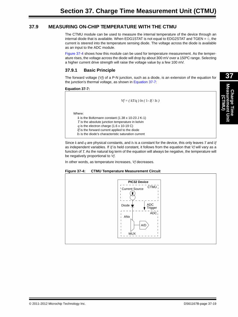
37.9 MEASURING ON-CHIP TEMPERATURE WITH THE CTMU The CTMU module can be used to measure the internal temperature of the device through aninternal diode that is available. When EDG1STAT is not equal to EDG2STAT and TGEN = 0, thecurrent is steered into the temperature sensing diode. The voltage across the diode is availableas an input to the ADC module.
Figure 37-4 shows how this module can be used for temperature measurement. As the temper-ature rises, the voltage across the diode will drop by about 300 mV over a 150ºC range. Selectinga higher current drive strength will raise the voltage value by a few 100 mV.
37.9.1 Basic PrincipleThe forward voltage (Vf) of a P-N junction, such as a diode, is an extension of the equation forthe junction’s thermal voltage, as shown in Equation 37-7:
Equation 37-7:
Since k and q are physical constants, and Is is a constant for the device, this only leaves T and Ifas independent variables. If If is held constant, it follows from the equation that Vf will vary as afunction of T. As the natural log term of the equation will always be negative, the temperature willbe negatively proportional to Vf.
In other words, as temperature increases, Vf decreases.
Figure 37-4: CTMU Temperature Measurement Circuit
Where:k is the Boltzmann constant (1.38 x 10⁻²³ J K-1) T is the absolute junction temperature in kelvin
q is the electron charge (1.6 x 10⁻¹⁹ C)
Vf = ( kT/q ) ln ( 1- If / Is )
If is the forward current applied to the diodeIs is the diode’s characteristic saturation current
PIC32 Device
ADC
CTMUCurrent Source
ADCTrigger
A/D
MUX
Diode
ANx
© 2011-2012 Microchip Technology Inc. DS61167B-page 37-19

PIC32 Family Reference Manual
37.10 OPERATION DURING SLEEP/IDLE MODES
37.10.1 Sleep ModeWhen the device enters any Sleep mode, the CTMU module’s current source is always disabled.If the CTMU is performing an operation that depends on the current source when Sleep mode isinvoked, the operation may not terminate correctly. Capacitance and time measurements mayreturn erroneous values.
37.10.2 Idle ModeThe behavior of the CTMU in Idle mode is determined by the CTMUSIDL bit (CTMUCON<13>).If the CTMUSIDL bit is cleared, the module will continue to operate in Idle mode. If theCTMUSIDL bit is set, the module’s current source is disabled when the device enters Idle mode.If the module is performing an operation when Idle mode is invoked, in this case, the results willbe similar to those with Sleep mode.
37.11 EFFECTS OF A RESET ON CTMUUpon Reset, all registers of the CTMU are cleared. This leaves the CTMU module disabled, itscurrent source is turned off and all configuration options return to their default settings. Themodule needs to be re-initialized following any Reset.
If the CTMU is in the process of taking a measurement at the time of Reset, the measurement willbe lost. A partial charge may exist on the circuit that was being measured and should be properlydischarged before the CTMU makes subsequent attempts to make a measurement. The circuit isdischarged by setting, and then clearing, the IDISSEN bit (CTMUCON<9>) while the ADC isconnected to the appropriate channel.
DS61167B-page 37-20 © 2011-2012 Microchip Technology Inc.

Section 37. Charge Time Measurement Unit (CTMU)C
harge Time
Measurem
ent Unit
(CTM
U)
37
37.12 RELATED APPLICATION NOTESThis section lists application notes that are related to this section of the manual. Theseapplication notes may not be written specifically for the PIC32 device family, but the concepts arepertinent and could be used with modification and possible limitations. The current applicationnotes related to the Charge Time Measurement Unit (CTMU) module are:
Title Application Note #No related application notes at this time. N/A
Note: Please visit the Microchip web site (www.microchip.com) for additional applicationnotes and code examples for the PIC32 family of devices.
© 2011-2012 Microchip Technology Inc. DS61167B-page 37-21

PIC32 Family Reference Manual
37.13 REVISION HISTORY
Revision A (March 2011)This is the initial released revision of this document.
Revision B (February 2012)This revision includes the following updates:
• Added Note 1 and Note 2 to 37.3.2 “Current Source”• Updated the last sentence of the first paragraph in 37.3.4 “Edge Status”• Added Note 1 to the CTMU Current Source Calibration Circuit (see Figure 37-2)• Removed Setup for CTMU Calibration Routines (formerly Example 37-1)• Updated the code in the Current Calibration Routine (see Example 37-1)• Updated the code in the Capacitance Calibration Routine (see Example 37-2)• Updated the code in the Routine for Capacitive Touch Switch Routine (see Example 37-3)• Minor updates to text and formatting were incorporated throughout the document
DS61167B-page 37-22 © 2011-2012 Microchip Technology Inc.
Note the following details of the code protection feature on Microchip devices:• Microchip products meet the specification contained in their particular Microchip Data Sheet.
• Microchip believes that its family of products is one of the most secure families of its kind on the market today, when used in the intended manner and under normal conditions.
• There are dishonest and possibly illegal methods used to breach the code protection feature. All of these methods, to our knowledge, require using the Microchip products in a manner outside the operating specifications contained in Microchip’s Data Sheets. Most likely, the person doing so is engaged in theft of intellectual property.
• Microchip is willing to work with the customer who is concerned about the integrity of their code.
• Neither Microchip nor any other semiconductor manufacturer can guarantee the security of their code. Code protection does not mean that we are guaranteeing the product as “unbreakable.”
Code protection is constantly evolving. We at Microchip are committed to continuously improving the code protection features of ourproducts. Attempts to break Microchip’s code protection feature may be a violation of the Digital Millennium Copyright Act. If such actsallow unauthorized access to your software or other copyrighted work, you may have a right to sue for relief under that Act.
Information contained in this publication regarding deviceapplications and the like is provided only for your convenienceand may be superseded by updates. It is your responsibility toensure that your application meets with your specifications.MICROCHIP MAKES NO REPRESENTATIONS ORWARRANTIES OF ANY KIND WHETHER EXPRESS ORIMPLIED, WRITTEN OR ORAL, STATUTORY OROTHERWISE, RELATED TO THE INFORMATION,INCLUDING BUT NOT LIMITED TO ITS CONDITION,QUALITY, PERFORMANCE, MERCHANTABILITY ORFITNESS FOR PURPOSE. Microchip disclaims all liabilityarising from this information and its use. Use of Microchipdevices in life support and/or safety applications is entirely atthe buyer’s risk, and the buyer agrees to defend, indemnify andhold harmless Microchip from any and all damages, claims,suits, or expenses resulting from such use. No licenses areconveyed, implicitly or otherwise, under any Microchipintellectual property rights.
© 2011-2012 Microchip Technology Inc.
Trademarks
The Microchip name and logo, the Microchip logo, dsPIC, KEELOQ, KEELOQ logo, MPLAB, PIC, PICmicro, PICSTART, PIC32 logo, rfPIC and UNI/O are registered trademarks of Microchip Technology Incorporated in the U.S.A. and other countries.
FilterLab, Hampshire, HI-TECH C, Linear Active Thermistor, MXDEV, MXLAB, SEEVAL and The Embedded Control Solutions Company are registered trademarks of Microchip Technology Incorporated in the U.S.A.
Analog-for-the-Digital Age, Application Maestro, chipKIT, chipKIT logo, CodeGuard, dsPICDEM, dsPICDEM.net, dsPICworks, dsSPEAK, ECAN, ECONOMONITOR, FanSense, HI-TIDE, In-Circuit Serial Programming, ICSP, Mindi, MiWi, MPASM, MPLAB Certified logo, MPLIB, MPLINK, mTouch, Omniscient Code Generation, PICC, PICC-18, PICDEM, PICDEM.net, PICkit, PICtail, REAL ICE, rfLAB, Select Mode, Total Endurance, TSHARC, UniWinDriver, WiperLock and ZENA are trademarks of Microchip Technology Incorporated in the U.S.A. and other countries.
SQTP is a service mark of Microchip Technology Incorporated in the U.S.A.
All other trademarks mentioned herein are property of their respective companies.
© 2011-2012, Microchip Technology Incorporated, Printed in the U.S.A., All Rights Reserved.
Printed on recycled paper.
ISBN: 978-1-62076-043-7
DS61167B-page 37-23
Microchip received ISO/TS-16949:2009 certification for its worldwide headquarters, design and wafer fabrication facilities in Chandler and Tempe, Arizona; Gresham, Oregon and design centers in California and India. The Company’s quality system processes and procedures are for its PIC® MCUs and dsPIC® DSCs, KEELOQ® code hopping devices, Serial EEPROMs, microperipherals, nonvolatile memory and analog products. In addition, Microchip’s quality system for the design and manufacture of development systems is ISO 9001:2000 certified.

DS61167B-page 37-24 © 2011-2012 Microchip Technology Inc.
AMERICASCorporate Office2355 West Chandler Blvd.Chandler, AZ 85224-6199Tel: 480-792-7200 Fax: 480-792-7277Technical Support: http://www.microchip.com/supportWeb Address: www.microchip.comAtlantaDuluth, GA Tel: 678-957-9614 Fax: 678-957-1455BostonWestborough, MA Tel: 774-760-0087 Fax: 774-760-0088ChicagoItasca, IL Tel: 630-285-0071 Fax: 630-285-0075ClevelandIndependence, OH Tel: 216-447-0464 Fax: 216-447-0643DallasAddison, TX Tel: 972-818-7423 Fax: 972-818-2924DetroitFarmington Hills, MI Tel: 248-538-2250Fax: 248-538-2260IndianapolisNoblesville, IN Tel: 317-773-8323Fax: 317-773-5453Los AngelesMission Viejo, CA Tel: 949-462-9523 Fax: 949-462-9608Santa ClaraSanta Clara, CA Tel: 408-961-6444Fax: 408-961-6445TorontoMississauga, Ontario, CanadaTel: 905-673-0699 Fax: 905-673-6509
ASIA/PACIFICAsia Pacific OfficeSuites 3707-14, 37th FloorTower 6, The GatewayHarbour City, KowloonHong KongTel: 852-2401-1200Fax: 852-2401-3431Australia - SydneyTel: 61-2-9868-6733Fax: 61-2-9868-6755China - BeijingTel: 86-10-8569-7000 Fax: 86-10-8528-2104China - ChengduTel: 86-28-8665-5511Fax: 86-28-8665-7889China - ChongqingTel: 86-23-8980-9588Fax: 86-23-8980-9500China - HangzhouTel: 86-571-2819-3187 Fax: 86-571-2819-3189China - Hong Kong SARTel: 852-2401-1200 Fax: 852-2401-3431China - NanjingTel: 86-25-8473-2460Fax: 86-25-8473-2470China - QingdaoTel: 86-532-8502-7355Fax: 86-532-8502-7205China - ShanghaiTel: 86-21-5407-5533 Fax: 86-21-5407-5066China - ShenyangTel: 86-24-2334-2829Fax: 86-24-2334-2393China - ShenzhenTel: 86-755-8203-2660 Fax: 86-755-8203-1760China - WuhanTel: 86-27-5980-5300Fax: 86-27-5980-5118China - XianTel: 86-29-8833-7252Fax: 86-29-8833-7256China - XiamenTel: 86-592-2388138 Fax: 86-592-2388130China - ZhuhaiTel: 86-756-3210040 Fax: 86-756-3210049
ASIA/PACIFICIndia - BangaloreTel: 91-80-3090-4444 Fax: 91-80-3090-4123India - New DelhiTel: 91-11-4160-8631Fax: 91-11-4160-8632India - PuneTel: 91-20-2566-1512Fax: 91-20-2566-1513Japan - OsakaTel: 81-66-152-7160 Fax: 81-66-152-9310Japan - YokohamaTel: 81-45-471- 6166 Fax: 81-45-471-6122Korea - DaeguTel: 82-53-744-4301Fax: 82-53-744-4302Korea - SeoulTel: 82-2-554-7200Fax: 82-2-558-5932 or 82-2-558-5934Malaysia - Kuala LumpurTel: 60-3-6201-9857Fax: 60-3-6201-9859Malaysia - PenangTel: 60-4-227-8870Fax: 60-4-227-4068Philippines - ManilaTel: 63-2-634-9065Fax: 63-2-634-9069SingaporeTel: 65-6334-8870Fax: 65-6334-8850Taiwan - Hsin ChuTel: 886-3-5778-366Fax: 886-3-5770-955Taiwan - KaohsiungTel: 886-7-536-4818Fax: 886-7-330-9305Taiwan - TaipeiTel: 886-2-2500-6610 Fax: 886-2-2508-0102Thailand - BangkokTel: 66-2-694-1351Fax: 66-2-694-1350
EUROPEAustria - WelsTel: 43-7242-2244-39Fax: 43-7242-2244-393Denmark - CopenhagenTel: 45-4450-2828 Fax: 45-4485-2829France - ParisTel: 33-1-69-53-63-20 Fax: 33-1-69-30-90-79Germany - MunichTel: 49-89-627-144-0 Fax: 49-89-627-144-44Italy - Milan Tel: 39-0331-742611 Fax: 39-0331-466781Netherlands - DrunenTel: 31-416-690399 Fax: 31-416-690340Spain - MadridTel: 34-91-708-08-90Fax: 34-91-708-08-91UK - WokinghamTel: 44-118-921-5869Fax: 44-118-921-5820
Worldwide Sales and Service
11/29/11