Secondary Ion Mass Spectrometry AMC Workshop SIMS.pdfSecondary Ion Mass Spectrometry . SIMS is an...
38
© 2016 University of Illinois Board of Trustees. All rights reserved. Secondary Ion Mass Spectrometry Timothy P. Spila, Ph.D. Frederick Seitz Materials Research Laboratory University of Illinois at Urbana-Champaign
Transcript of Secondary Ion Mass Spectrometry AMC Workshop SIMS.pdfSecondary Ion Mass Spectrometry . SIMS is an...

© 2016 University of Illinois Board of Trustees. All rights reserved.
Secondary Ion Mass Spectrometry
Timothy P. Spila, Ph.D.
Frederick Seitz Materials Research Laboratory University of Illinois at Urbana-Champaign

© 2016 University of Illinois Board of Trustees. All rights reserved.
Secondary Ion Mass Spectrometry
SIMS is an analytical technique based on the measurement of the mass of ions ejected from a solid surface after the surface has been bombarded with high energy (1-25 keV) primary ions.
Primary Ions Secondary Ions

© 2016 University of Illinois Board of Trustees. All rights reserved.
Technique Comparison
© 2016 University of Illinois Board of Trustees. All rights reserved.
Block Diagram of SIMS Technique

© 2016 University of Illinois Board of Trustees. All rights reserved.
Comparison of Static and Dynamic SIMS
TECHNIQUE DYNAMIC STATIC FLUX ~1017 ions/cm2
(minimum dose density) < 1013 ions/cm2 (per experiment)
INFORMATION Elemental Elemental + Molecular
SENSITIVITY < 1 ppm (ppb for some elements)
1 ppm
TYPE OF ANALYSIS Depth Profile Mass Spectrum 3D Image Depth Profile
Surface Mass Spectrum 2D Surface Ion Image
SAMPLING DEPTH 10 monolayers 2 monolayers
SPATIAL RESOLUTION
Cameca ims 5f Probe mode: 200 nm Microscope mode: 1 µm
PHI TRIFT III 0.1 µm
SAMPLE DAMAGE Destructive in analyzed area – up to 500 µm per area
Minimal

© 2016 University of Illinois Board of Trustees. All rights reserved.
Magnetic Sector Mass Spectrometer
CAMECA ims 5f
PRIMARY ION COLUMN
SECONDARY ION COLUMN

© 2016 University of Illinois Board of Trustees. All rights reserved.
Time of Flight Mass Spectrometer
Physical Electronics TRIFT III TOF-SIMS
Sam
ple
Cs+ or O2+
Au+
Pre-Spectrometer Blanker
SED
Contrast Diaphragm
Energy Slit
Post- Spectrometer Blanker
ESA 1
ESA 2 ESA 3
2
21 mveV =

© 2016 University of Illinois Board of Trustees. All rights reserved.
Ion Beam Sputtering
Sputtered species include: • Monoatomic and polyatomic particles of sample material (positive, negative or neutral) • Resputtered primary species (positive, negative or neutral) • Electrons • Photons

© 2016 University of Illinois Board of Trustees. All rights reserved.
MD Simulation of ion impact
Enhancement of Sputtering Yields due to C60 vs. Ga Bombardment of Ag{111} as Explored by Molecular Dynamics Simulations, Z. Postawa, B. Czerwinski, M. Szewczyk, E. J. Smiley, N. Winograd and B. J. Garrison, Anal. Chem., 75, 4402-4407 (2003). Animations downloaded from http://galilei.chem.psu.edu/sputtering-animations.html.

© 2016 University of Illinois Board of Trustees. All rights reserved.
Quantitative Surface Analysis: SIMS
In SIMS, the yield of secondary ions is strongly influenced by the electronic state of the material being analyzed.
Ism = secondary ion current of species m
Ip = primary particle flux ym = sputter yield α+ = ionization probability to positive ions θm = factional concentration of m in the layer η = transmission of the analysis system
ηθα mmpms yII +=

© 2016 University of Illinois Board of Trustees. All rights reserved.
Total Ion Sputtering Yield
+
First principles prediction of ion sputter yields is not possible with this technique.
Courtesy of Prof. Rockett
Sputter yield: ratio of number of atoms sputtered to number of impinging ions, typically 5-15
Ion sputter yield: ratio of ionized atoms sputtered
to number of impinging ions, 10-6 to 10-2
Ion sputter yield may be influenced by: •Matrix effects •Surface coverage of reactive elements •Background pressure in the sample environment •Orientation of crystallographic axes with respect to the sample surface •Angle of emission of detected secondary ions

© 2016 University of Illinois Board of Trustees. All rights reserved.
Effect of Primary Beam on Secondary Ion Yields
Oxygen bombardment When sputtering with an oxygen beam, the concentration of oxygen increases in the surface layer and metal-oxygen bonds are present in an oxygen-rich zone. When the bonds break during the bombardment, secondary ion emission process, oxygen becomes negatively charged because of its high electron affinity and the metal is left with the positive charge. Elements in yellow analyzed with oxygen bombardment, positive secondary ions for best sensitivity. Cesium bombardment When sputtering with a cesium beam, cesium is implanted into the sample surface which reduces the work function allowing more secondary electrons to be excited over the surface potential barrier. With the increased availability of electrons, there is more negative ion formation. Elements in green analyzed with cesium, negative secondary ions for best sensitivity.
Graphics courtesy of Charles Evans & Associates web site http://www.cea.com

© 2016 University of Illinois Board of Trustees. All rights reserved.
Relative Secondary Ion Yield Comparison
From Storms, et al., Anal. Chem. 49, 2023 (1977).

© 2016 University of Illinois Board of Trustees. All rights reserved.
Relative Secondary Ion Yield Comparison
From Storms, et al., Anal. Chem. 49, 2023 (1977).

© 2016 University of Illinois Board of Trustees. All rights reserved.
Determination of RSF Using Ion Implants
ii
m
IIRSF ρ=
Graphics courtesy of Charles Evans & Associates web site http://www.cea.com
CdIIdCtIRSF
bi
m
−=
∑φ
Level Profile:
Gaussian Profile:
RSF = Relative Sensitivity Factor Im, Ii = ion intensity (counts/sec) ρ = atom density (atoms/cm3) φ = implant fluence (atoms/cm2)
ηθα mmpms yII +=
C = # measurement cycles t = analysis time (s/cycle) d = crater depth (cm) Ib = background ion counts
Where:

© 2016 University of Illinois Board of Trustees. All rights reserved.
Positive and Negative Secondary Ions
0 100 200 300 400 500 600 70010-1
1
10
102
103
104
105
106
Ion implanted P standard
O+2 beam
Si P
Cs+ beam Si P
Coun
ts /
sec
Depth (nm)0 100 200 300 400 500 600 700
1017
1018
1019
1020
1021
1022
1023 Ion implanted P standard
O+2 beam
Si P
Cs+ beam Si P
Conc
entra
tion
(ato
ms/
cm3 )
Depth (nm)

© 2016 University of Illinois Board of Trustees. All rights reserved.
Definition of Mass Resolution
Graphic courtesy of Charles Evans & Associates web site http://www.cea.com
Mass resolution defined by m/∆m Mass resolution of ~1600 required to resolve 32S from 16O2

© 2016 University of Illinois Board of Trustees. All rights reserved.
Depth Profile Application with Hydrogen
Detects hydrogen Large dynamic range

© 2016 University of Illinois Board of Trustees. All rights reserved.
Isotopic Analysis
(b)
(c)
0 50 100 150 200 250 300 350Sputter Time (min.)
0
20
40
60
80
100
Ni Al3NiO, NiAl O , Al O 42 32NiO
Oxy
gen
Ion
Yiel
d(%
Lin
ear C
ount
s)
16M O
M O18
(a)
AE
S A
tom
ic C
onc
en
tra
tion
(%
)
0
10
20
30
40
50
70
60
Ni Al 600 C: 4 h 18O , 16 h 16O3 2 2R.T. Haasch, A.M. Venezia, and C.M. Loxton. J. Mater.Res., 7, 1341 (1992).
(a) AES composition depth profile (b) SIMS isotopic oxygen diffusion profile expressed as a
percentage of the total oxygen (c) Schematic of layered oxide structure
(a) (b)
(c)
M16O M18O
16O+
18O+ O
Al
Ni

© 2016 University of Illinois Board of Trustees. All rights reserved.
B Depth Profile in Si(001)
SIMS depth profiles through a B modulation-doped Si(001):B film grown by GS-MBE from Si2H6 and B2H6 at Ts=600 °C. The incident Si2H6 flux was JSi2H6 = 2.2x1016 cm-2 s-1 while the B flux JB2H6 was varied from 8.4x10¹³ to 1.2x1016 cm-2 s-1. The deposition time for each layer was constant at 1 h.
G. Glass, H. Kim, P. Desjardins, N. Taylor, T. Spila, Q. Lu, and J. E. Greene. Phys. Rev. B, 61,7628 (2000).

© 2016 University of Illinois Board of Trustees. All rights reserved.
Depth Resolution and Ion Beam Mixing
SIMS depth profiles through a B δ-doped layers in a Si(001) film grown by GS-MBE from Si2H6 at TS=700 °C. The Si2H6, flux, JSi2H6, was 5X1016 cm-2 s-1 while the B2H6 flux, JB2H6 varied from 0.16-7.8X1014 cm-2 s-1. The inset shows the two-dimensional B concentration NB
2D as a function of JB2H6.
Q. Lu, T. R. Bramblett, N.-E. Lee, M.-A. Hasan, T. Karasawa, and J. E. Greene. J. Appl. Phys. 77, 3067 (1995).

© 2016 University of Illinois Board of Trustees. All rights reserved.
Electrolessly etched silicon nanowire arrays
Dope NW tips by SODs
J.S Sadhu, H. Tian, T. Spila, J. Kim, B. Azeredo, P. Ferreira, and S. Sinha. Nanotechnology 25, 375701 (2014).

© 2016 University of Illinois Board of Trustees. All rights reserved.
Transition-Metal Accumulation on Anodes in Li-ion Batteries
1
10
100
1000
10000
100000
0 2000 4000 6000 80001
10
100
1000
10000
100000
0 2000 4000 6000 8000
1
10
100
1000
10000
100000
0 2000 4000 6000 80001
10
100
1000
10000
100000
0 2000 4000 6000 8000
Sputtering time, s
Cou
nts p
er se
cond
Mn
Fr
F
A
A
FFr
C
Co
Fr
F
A
Ni
Fr
F
A
1
10
100
1000
10000
100000
0 2000 4000 6000 80001
10
100
1000
10000
100000
0 2000 4000 6000 8000
1
10
100
1000
10000
100000
0 2000 4000 6000 80001
10
100
1000
10000
100000
0 2000 4000 6000 8000
Sputtering time, s
Cou
nts p
er se
cond
Mn
Fr
F
A
A
FFr
C
Co
Fr
F
A
Ni
Fr
F
A

© 2016 University of Illinois Board of Trustees. All rights reserved.
Static and Dynamic SIMS
Dynamic SIMS Static SIMS
•Material removal •Elemental analysis •Depth profiling
•Ultra surface analysis •Elemental or molecular analysis •Analysis complete before significant fraction of molecules destroyed
Courtesy Gregory L. Fisher, Physical Electronics

© 2016 University of Illinois Board of Trustees. All rights reserved.
Extreme Mass Range
Mass (amu)
Tota
l Cou
nts

© 2016 University of Illinois Board of Trustees. All rights reserved.
Trace Analysis GaAs Wafer
85.85 85.90 85.95 86.00 Mass [m/z]
0
5000
10000
15000
20000
Coun
ts
GaOH
GaNH3 m/∆m = 11,600
Si Wafer
38.94 38.96 38.98 39.00 39.02 39.04 Mass [m/z]
0 10
1 10
2 10
3 10
4 10
5 10
6 10
Coun
ts K
C3H3
C2HN
No sputtering to remove organics on surface. Large C3H3 peak does not have a tail to lower mass which would obscure C2HN and K.
© 2016 University of Illinois Board of Trustees. All rights reserved.
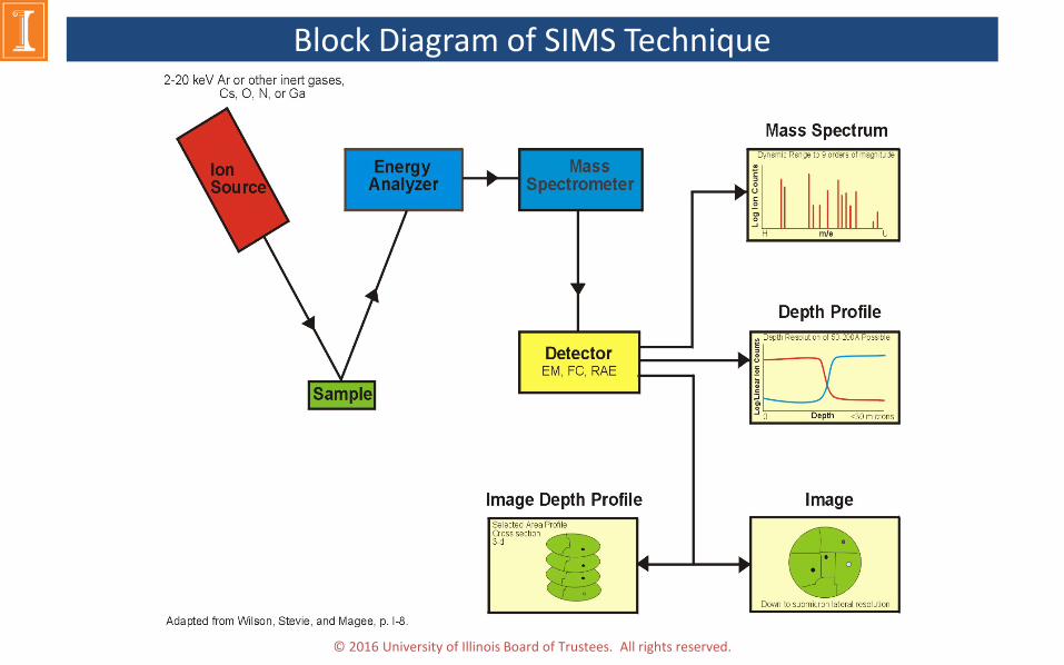
InAs/GaAs Quantum Dots
In+ Linescans of Quantum Dots
µm 0 0.5 1.0 1.5 2.0
0
5
10
15
20
µm 0 0.5 1.0 1.5
0
5
10
15
µm 0 0.5 1.0 1.5 2.0 2.5 3.0 3.5
0
5
10
15
20
25
Cts: 550893; Max: 36; Scale: 1µm

© 2016 University of Illinois Board of Trustees. All rights reserved.
GaAs/AlGaAs Depth Profile
Al
Ga
Analysis beam: 15kV Ga+
Sputter Beam: 300V O2+
with oxygen flood

© 2016 University of Illinois Board of Trustees. All rights reserved.
Defect Engineering via Near-Surface Electrostatic Effects
Charged point defects interact with space charge in the near-surface region via 3 mechanisms 1. Field-induced drift (O in TiO2)1
2. Change in charge state of defect with local potential (B in Si)2
3. Potential energy-dependent formation energy of VO (O in SrTiO3)3
18O piles up in the first 10-30 nm in ZnO and TiO21
• Amount of pile-up (P) = integrated area between pile-up and bulk extrapolated profiles
Analytical model quantifies effects4 • Drift opposite to diffusion causes pile-up • Drift in diffusion direction depletes near-surface of mobile
defects • P increases linearly with time & flux, quadratically with VS • Vs of only a few meV can cause the amount of pile-up
observed
1P. Gorai et al., Appl. Phys. Lett. 103, 141601 (2013). 2P. Gorai et al., J. Appl. Phys. 111, 094510 (2012). 3R.A. De Souza and M. Martin, PCCP 10, 2356 (2008). 4P. Gorai and E. G. Seebauer, Appl. Phys. Lett. 105, 021604 (2014).

© 2016 University of Illinois Board of Trustees. All rights reserved.
200 400 600 800 1000Time (Seconds)
010
110
210
310
410
510
Coun
ts
Total_Ion
U
UO
Nd
NdO
200 400 600 800 1000Time (Seconds)
010
110
210
310
410
510
Coun
ts
Total_Ion
UUO
Nd
NdO
Depth Profile Beam Alignment

© 2016 University of Illinois Board of Trustees. All rights reserved.
TOF-SIMS Imaging of Patterned Sample
O OO
Br
OS
O OSi
O
OH
O hν (∼375 nm)
H2O
OS
O OSi
O
OH
OH
Courtesy Josh Ritchey, Audrey Bowen, Ralph Nuzzo and Jeffrey Moore, University of Illinois
400 µm S
400 µm Br
50 µm Br

© 2016 University of Illinois Board of Trustees. All rights reserved.
TOF-SIMS Ion Images of an Isolated Neuron First Images of Vitamin E Distribution in a Cell
Courtesy E.B. Monroe, J.C. Jurchen, S.S. Rubakhin, J.V. Sweedler. University of Illinois at Urbana-Champaign

© 2016 University of Illinois Board of Trustees. All rights reserved.
TOF-SIMS Ion Images of Songbird Brain
Selected ion images from the songbird brain. Each ion image consists of ~11.5 million pixels within the tissue section and is the combination of 194 individual 600m×600m ion images prepared on the same relative intensity scale. Ion images are (A) phosphate PO3− (m/z 79.0); (B) cholesterol (m/z 385.4); (C) arachidonic acid C20:4 (m/z 303.2); (D) palmitic acid C16:0 (m/z 255.2); (E) palmitoleic acid C16:1 (m/z 253.2); (F) stearic acid C18:0 (m/z 283.3); (G) oleic acid C18:1 (m/z 281.2); (H) linoleic acid C18:2 (m/z 279.23); and (I) -linolenic acid C18:3 (m/z 277.2). Scale bars = 2 mm.
Courtesy Kensey R. Amaya, Eric B. Monroe, Jonathan V. Sweedler, David F. Clayton. International Journal of Mass Spectrometry 260, 121 (2007).
MRL Biological Conference 2016 November 2 & 3, 2016
www.mrl.illinois.edu/bio2016

© 2016 University of Illinois Board of Trustees. All rights reserved.
Diamond-Like-Carbon Friction Testing
wear tracks and scars formed on DLC-coated disk and ball sides during test in dry oxygen
DLC coated ball
DLC coated disk
Oxygen Carbon C + O Overlay
Courtesy O.L. Eryilmaz and A. Erdemir Energy Systems Division, Argonne National Laboratory Argonne, IL 60439 USA

© 2016 University of Illinois Board of Trustees. All rights reserved.
3-D TOF-SIMS imaging of DLC Wear track from hydrogenated DLC tested in dry nitrogen Courtesy O.L. Eryilmaz and A. Erdemir Energy Systems Division, Argonne National Laboratory Argonne, IL 60439 USA

© 2016 University of Illinois Board of Trustees. All rights reserved.
3-D TOF-SIMS Movies of DLC
H CH C2H C2H2 O
NFC6 H2 Environment TOF-SIMS Images Courtesy O.L. Eryilmaz and A. Erdemir Energy Systems Division, Argonne National Laboratory Argonne, IL 60439 USA

© 2016 University of Illinois Board of Trustees. All rights reserved.
SIMS Summary
Probe/Detected Species Information Surface Mass Spectrum 2D Surface Ion Image Elemental Depth Profiling 3D Image Depth Profiling Elements Detectable H and above Sensitivity ppb - atomic % Analysis Diameter/Sampling Depth ~1 µm - several mm/0.5 - 1nm

Thanks to our sponsors!
© 2016 University of Illinois Board of Trustees. All rights reserved.
Platinum Sponsors