SD/MMC SPI Core El Camino Camino GmbH 4 SD/MMC SPI Core - with Avalon Interface Figure 3: SOPC...
14
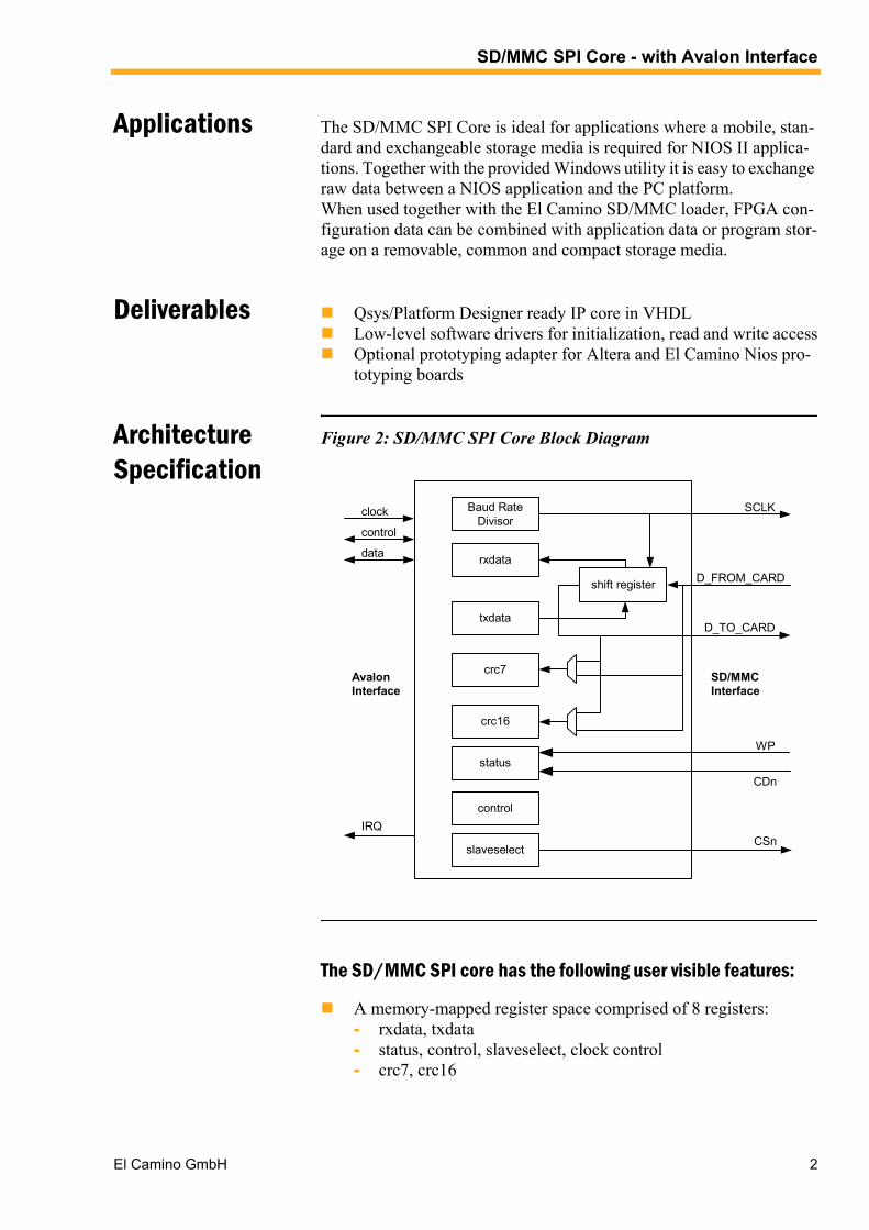
El Camino Training - Engineering - Consultancy El Camino GmbH 1 SD/MMC SPI Core with Avalon Interface General Description The SD/MMC SPI Core with Avalon Interface allows you to easily con- nect Qsys or Platform Designer systems to standard MultiMediaô Card (MMC) and Secure Digital Card (SD) flash based memory devices. The MultiMediaCard and SD-Cards are universal, low cost data storage and communication media, which are generally available and widely used in consumer products such as digital cameras or cellular phones. The SD/MMC SPI Core is fully compliant with Qsys and Platform Designer and integrates easily into any Qsys/Platform Designer generated sys- tem. For the NIOS II processor, El Camino provides low-level driver rou- tines for the SD/MMC SPI Core. The drivers provide universal access routines for MMC and SD memory devices. Therefore you do not need to write any additional low level code to read or write raw data from or to MMC/SD cards. Figure 1: Block Diagram Features More than 2400 kByte/s read and 2400 kByte/s write performance Supports MultiMediaCard (MMC) and Secure Digital Card (SD, SDHC, SDXC) in SPI mode Variable data rate up to 25 Mbps (SD only), 20 Mbps (SD/MMC) Hardware assisted CRC calculation Low-level drivers included Windows utility for raw data read/write access on PC platform Optional Stand-Alone FAT12/16/32 file system library Optional prototyping adapter for Altera and El Camino NIOS development boards MultiMediaCard/ SD Card SD/MMC SPI Core from El Camino FPGA Avalon Switch Fabric Avalon CPU or Bridge Other Avalon Masters/Slaves S M M/S February 2018, Version 2.2
Transcript of SD/MMC SPI Core El Camino Camino GmbH 4 SD/MMC SPI Core - with Avalon Interface Figure 3: SOPC...

El CaminoTraining - Engineering - Consultancy
El Camino GmbH 1
SD/MMC SPI Corewith Avalon Interface
General Description
The SD/MMC SPI Core with Avalon Interface allows you to easily con-nect Qsys or Platform Designer systems to standard MultiMediaô Card (MMC) and Secure Digital Card (SD) flash based memory devices. The MultiMediaCard and SD-Cards are universal, low cost data storage and communication media, which are generally available and widely used in consumer products such as digital cameras or cellular phones. The SD/MMC SPI Core is fully compliant with Qsys and Platform Designer and integrates easily into any Qsys/Platform Designer generated sys-tem.For the NIOS II processor, El Camino provides low-level driver rou-tines for the SD/MMC SPI Core. The drivers provide universal access routines for MMC and SD memory devices. Therefore you do not need to write any additional low level code to read or write raw data from or to MMC/SD cards.
Figure 1: Block Diagram
Features More than 2400 kByte/s read and 2400 kByte/s write performanceSupports MultiMediaCard (MMC) and Secure Digital Card (SD, SDHC, SDXC) in SPI modeVariable data rate up to 25 Mbps (SD only), 20 Mbps (SD/MMC)Hardware assisted CRC calculationLow-level drivers includedWindows utility for raw data read/write access on PC platformOptional Stand-Alone FAT12/16/32 file system libraryOptional prototyping adapter for Altera and El Camino NIOS development boards
MultiMediaCard/SD Card
SD/MMCSPI Corefrom ElCamino
FPGAA
valo
n S
witc
h Fa
bric
Avalon CPUor
Bridge
Other AvalonMasters/Slaves
S M
M/S
February 2018, Version 2.2
SD/MMC SPI Core - with Avalon Interface
Applications The SD/MMC SPI Core is ideal for applications where a mobile, stan-dard and exchangeable storage media is required for NIOS II applica-tions. Together with the provided Windows utility it is easy to exchange raw data between a NIOS application and the PC platform.When used together with the El Camino SD/MMC loader, FPGA con-figuration data can be combined with application data or program stor-age on a removable, common and compact storage media.
Deliverables Qsys/Platform Designer ready IP core in VHDLLow-level software drivers for initialization, read and write accessOptional prototyping adapter for Altera and El Camino Nios pro-totyping boards
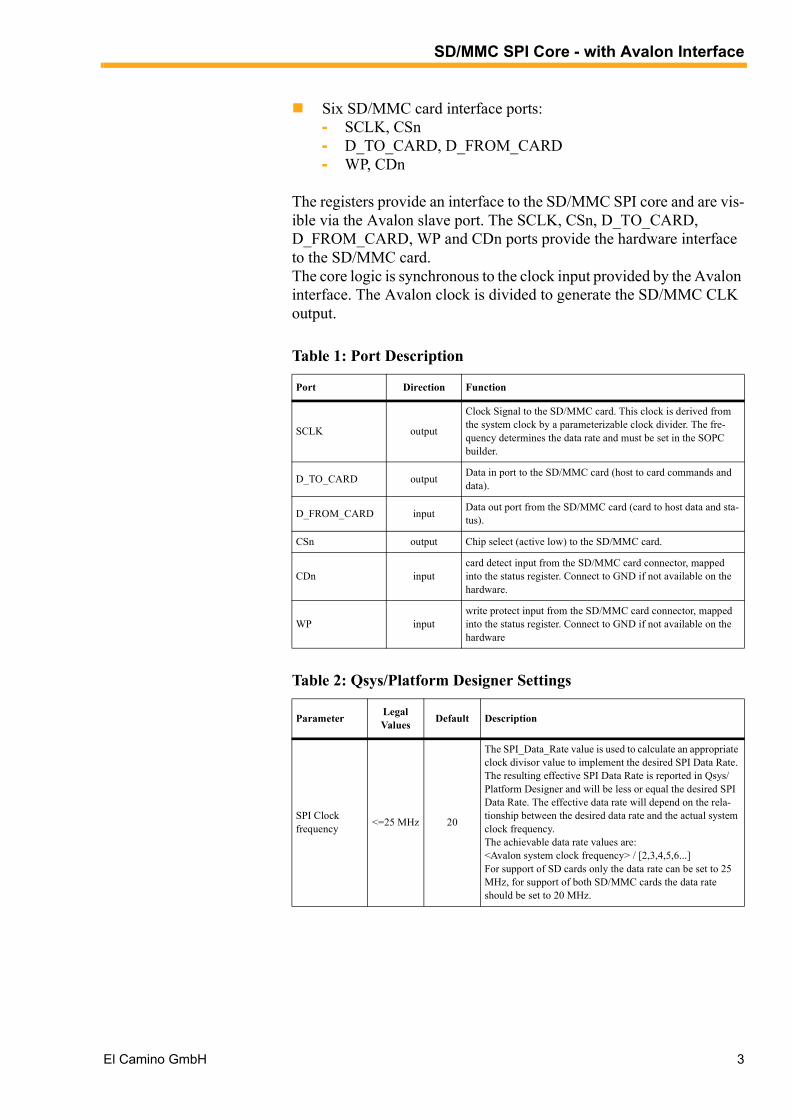
Architecture Specification
Figure 2: SD/MMC SPI Core Block Diagram
The SD/MMC SPI core has the following user visible features:
A memory-mapped register space comprised of 8 registers:- rxdata, txdata- status, control, slaveselect, clock control- crc7, crc16
Baud RateDivisor
rxdata
txdata
status
shift register
control
slaveselect
crc7
crc16
clock
control
data
IRQ
SCLK
D_FROM_CARD
D_TO_CARD
CSn
AvalonInterface
SD/MMCInterface
WP
CDn
El Camino GmbH 2
SD/MMC SPI Core - with Avalon Interface
Six SD/MMC card interface ports:- SCLK, CSn- D_TO_CARD, D_FROM_CARD- WP, CDn
The registers provide an interface to the SD/MMC SPI core and are vis-ible via the Avalon slave port. The SCLK, CSn, D_TO_CARD, D_FROM_CARD, WP and CDn ports provide the hardware interface to the SD/MMC card.The core logic is synchronous to the clock input provided by the Avalon interface. The Avalon clock is divided to generate the SD/MMC CLK output.
Table 1: Port Description
Port Direction Function
SCLK output
Clock Signal to the SD/MMC card. This clock is derived from the system clock by a parameterizable clock divider. The fre-quency determines the data rate and must be set in the SOPC builder.
D_TO_CARD output Data in port to the SD/MMC card (host to card commands and data).
D_FROM_CARD input Data out port from the SD/MMC card (card to host data and sta-tus).
CSn output Chip select (active low) to the SD/MMC card.
CDn inputcard detect input from the SD/MMC card connector, mapped into the status register. Connect to GND if not available on the hardware.
WP inputwrite protect input from the SD/MMC card connector, mapped into the status register. Connect to GND if not available on the hardware
Table 2: Qsys/Platform Designer Settings
Parameter Legal Values Default Description
SPI Clockfrequency <=25 MHz 20
The SPI_Data_Rate value is used to calculate an appropriate clock divisor value to implement the desired SPI Data Rate. The resulting effective SPI Data Rate is reported in Qsys/Platform Designer and will be less or equal the desired SPI Data Rate. The effective data rate will depend on the rela-tionship between the desired data rate and the actual system clock frequency.The achievable data rate values are:<Avalon system clock frequency> / [2,3,4,5,6...]For support of SD cards only the data rate can be set to 25 MHz, for support of both SD/MMC cards the data rate should be set to 20 MHz.
El Camino GmbH 3

SD/MMC SPI Core - with Avalon Interface
Figure 3: Qsys/Platform Desginer GUI
Figure 4: Connecting the SD/MMC SPI Core
(1)Pull-up resistors are 10kOhm
Register Model
An Avalon master peripheral controls and communicates with the SD/MMC SPI core via the 8 16-bit registers, shown in the following table:
SCLK
D_TO_CARD
CSn
D_FROM_CARD
CDn
AvalonInterface
SD/MMC SPI Core
MMC/ SD
(top view)CS - 1
DataIn - 2VSS - 3VDD - 4CLK - 5VSS - 6
DataOut - 7
VCC(1)
rsv - 8
rsv - 9
WP
VCC VCC VCC VCC VCC
El Camino GmbH 4
SD/MMC SPI Core - with Avalon Interface
(1) A write operation to the status register clears the roe, toe and e bits
rxdata Register
A master peripheral reads received data from the rxdata register. When the receive shift register receives a full 8 bits of data, the status registerís rrdy bit is set to 1 and the data is transferred into the rxdata register. Reading the rxdata register clears the rrdy bit. Writing to the rxdata reg-ister has no effect. New data is always transferred into the rxdata regis-ter, whether or not the previous data was retrieved. If rrdy is 1 when data is transferred into the rxdata register (i.e., the previous data was not re-trieved), a receive overrun error occurs and the status registerís roe bit is set to 1. In this case, the contents of rxdata are undefined.
txdata Register
A master peripheral writes data to be transmitted into the txdata register. When the status registerís trdy bit is 1, it indicates that the txdata regis-ter is ready for new data. The trdy bit is set to 0 whenever the txdata reg-ister is written. The trdy bit is set to 1 after data is transferred from the txdata register into the transmitter shift register, which readies the txda-ta holding register to receive new data.A master peripheral should not write to the txdata register until the transmitter is ready for new data. If trdy is 0 and a master peripheral writes new data to the txdata register, a transmit-overrun error occurs and the status registerís toe bit is set to 1. In this case, the new data is ignored, and the content of txdata remains unchanged.As an example, assume that the SD/MMC SPI core is idle (i.e., the tx-data register and transmit shift register are empty), when a CPU writes a data value into the txdata holding register. The trdy bit is set to 0 mo-mentarily, but after the data in txdata is transferred into the transmitter shift register, trdy returns to 1. The CPU writes a second data value into
Table 3: Register Map for SD/MMC IP Core
InternalAddress
RegisterName 15..12 11 10 9 8 7 6 5 4 3 2 1 0
0 rxdata RXDATA
1 txdata TXDATA
2 status (1) CD E RRDY TRDY TMT TOE ROE WP MS
3 control ICD SSO IE IRRDY ITRDY ITOE IROE CRCDIR
CRCCLEAR
CNT START
4 crc7 CRC7 1
5 slaveselect SELECT
6 clock control SYS_CLK SPI_CLK_DIVISOR
7 crc16 CRC16
El Camino GmbH 5
SD/MMC SPI Core - with Avalon Interface
the txdata register, and again the trdy bit is set to 0. This time the shift register is still busy transferring the original data value, so the trdy bit remains at 0 until the shift operation completes. When the operation completes, the second data value is transferred into the transmitter shift register and the trdy bit is again set to 1.
status Register
The status register consists of bits that indicate status conditions in the SD/MMC SPI core. Each bit is associated with a corresponding inter-rupt-enable bit in the control register, as discussed in ì control Registerî .A master peripheral can read status at any time without changing the value of any bits. Writing status does clear the roe, toe and e bits. The next table describes the individual bits of the status register.
control Register
The control register consists of data bits to control the SD/MMC SPI coreís operation. A master peripheral can read the control register at any time without changing the value of any bits. Most bits (ICD, IROE, ITOE, ITRDY, IRRDY, and IE) in the control register control interrupts for status conditions represented in the status register. For example, bit 1 of status is ROE (receiver-overrun error), and bit 1 of control is IROE,
Table 4: status Register Bits
# Name Description
0 MSMillisecond TimerOne millisecond after the CNT START bit in the control register was set to 1 this bit is set to 1. This bit is automatically reset after reading from the status register.
1 WP Write ProtectThe WP bit mirrors the status of the write protect input of the SD/MMC core.
3 ROEReceive-overrun errorThe ROE bit is set to 1 if new data is received while the rxdata register is full (that is, while the RRDY bit is 1). In this case, the new data overwrites the old. Writing to the status register clears the ROE bit to 0.
4 TOETransmitter-overrun errorThe TOE bit is set to 1 if new data is written to the txdata register while it is still full (that is, while the TRDY bit is 0). In this case, the new data is ignored. Writing to the status register clears the TOE bit to 0.
5 TMT Transmitter shift-register emptyThe TMT bit is set to 0 when a transaction is in progress and set to 1 when the shift register is empty.
6 TRDY Transmitter readyThe TRDY bit is set to 1 when the txdata register is empty.
7 RRDY Receiver readyThe RRDY bit is set to 1 when the rxdata register is full.
8 EErrorThe E bit is the logical OR of the TOE and ROE bits. This is a convenience for the programmer to detect error condi-tions. Writing to the status register clears the E bit to 0.
11 CD Card DetectThe CD bit mirrors the status of the card detect input of the SD/MMC core.
El Camino GmbH 6

SD/MMC SPI Core - with Avalon Interface
which enables interrupts for the ROE condition. The SPI core asserts an interrupt request when the corresponding bits in status and control are both 1. The next table describes the individual bits of the control regis-ter.
After reset, all bits of the control register are set to 0. All interrupts are disabled and no cs_n signal is asserted after reset.
slaveselect Register
The slaveselect register is a bit mask for the cs_n signals driven by SD/MMC SPI core. The core has only one cs_n output mapped to bit 0 of the slaveselect register. During a serial shift operation, the SPI master selects only the slave device(s) specified in the slaveselect register. Upon reset, bit 0 is set to 1, and all other bits are cleared to 0. Thus, after a device reset, the SD/MMC card is automatically selected.
clock control Register
The uper half of the clock control register is read only and contains the system clock frequency that was set in the SOPC builder. This register is used to pass the actual system clock frequency to the sofware driver.The lower half of the clock control register can be read and written. A read returns the inital divisor as set by the SOPC builder. The software driver can update the value of the register in order to change the SPI clock frequency. A read however will always return the intial value so
Table 5: control Register Bits
# Name Description
0 CNT START Counter StartWriting a 1 to this bit starts a one millisecond counter. When the counter expires the MS bit is set in the status register.
1 CRC CLEARCRC Register ClearThis bit resets the CRC7 and CRC16 registers and prepares new CRC calculations base on the data sent or received by the core.
2 CRC DIRCRC DirectionThis bit connects the CRC7 and CRC16 registers to either the transmit or receive channel. Setting this bit to 1 calculates CRCs on outgoing data. Setting this bit to 0 calculates CRCs on incoming data.
3 IROE Setting IROE to 1 enables interrupts for receive-overrun errors.
4 ITOE Setting ITOE to 1 enables interrupts for transmitter-overrun errors.
6 ITRDY Setting ITRDY to 1 enables interrupts for transmitter ready conditions.
7 IRRDY Setting IRRDY to 1 enables interrupts for the receiver ready condition.
8 IE Setting IE to 1 enables interrupts for any error condition
10 SSOSetting SSO to 1 forces the SD/MMC SPI core to drive its cs_n output, regardless of whether a serial shift operation is in progress or not. The slaveselect register controls which cs_n outputs are asserted. sso can be used to transmit or receive data of arbitrary size (i.e., greater than 16 bits).
11 ICD Setting ICD to 1 enables interrupts for card detect conditions
El Camino GmbH 7
SD/MMC SPI Core - with Avalon Interface
this value can be restored after a different divisor was written by the software driver. The regiser should only be written while thereís no ac-tive transfer because otherwise transfered data may become corrupted.
ResourceUtilization andPerformance
The following results are based on synthesis and place & route in Quartus II Version 9.0 SP1. The maximum frequency of the data trans-fer is limited by both the maximum system frequency of the SOPC builder block and the maximum SCLK frequency of the SD/MMC card.
The following table shows some exemplary performance numbers. The actual performance will depend on the NIOS II CPU used, the clock fre-quencies used in the system, the SPI clock frequency and especially for writing, on the SD/MMC card used. The performance of the FAT file sytem will further depend on the fragmentation.
Software Support
Basic Concept
The SD/MMC SPI peripheral is integrated into the HAL generic device model classes as a FLASH memory device.
The HAL provides a generic device model for non-volatile flash mem-ory devices such as SD/MMC cards. The HAL API provides functions to write data to flash. For example, you can use these functions to im-plement a SD/MMC-based filing subsystem.Although it is not necessary for general, parallel FLASH devices, the HAL API also provides functions to read flash. For most flash devices, programs can treat the flash memory space as simple memory when reading, and do not need to call special HAL API functions. If the flash device has a special protocol for reading data, just like SD/MMC cards, you must use the HAL API to both read and write data.
Table 6: Resources (support not limited to these device families)
Device Family Ressource
Cyclone V 121 ALMs
Stratix V 119 ALMs
Arria 10 119 ALMs
Table 7: Performance
Platform NIOS CPUAavalon System Clock
SPI Clock Low LevelRead
Low LevelWrite
FAT 32Read
FAT 32Write
Altera NEEK Cyclone III Kitsync. SRAM (1 cycle/access) fast 100 MHz 25 MHz 2486 kByte/s 2410 kByte/s 2469 kByte/s 2380 kByte/s
El Camino GmbH 8
SD/MMC SPI Core - with Avalon Interface
The following two NIOS II HAL APIs provide a different level of ac-cess to the flash:
Simple flash accessa simple API for writing buffers into flash and reading them back, which in general does not preserve the prior contents of other flash erase blocks.
Fine-grained flash accessfiner-grained functions for programs that need control over writ-ing or erasing individual blocks. This functionality is generally required for managing a file subsystem.
With SD/MMC cards you can write single bytes without the need to erase whole blocks or sectors. So even when using simple flash access all data within a sector or block is preserved even when not writing the complete sector or block. Only for compatibility reasons with other flash devices it might make sense to use fine-grained flash access even with SD/MMC cards.
The API functions for accessing flash devices are defined in alt_flash.h.
Simple Flash Access
This interface comprises:alt_flash_open_dev(), alt_write_flash(), alt_read_flash(), andalt_flash_close_dev().Writing and Reading can start at any address and can be of any length as long as one stays within the boundarys of the SD/MMC card. For maximum compatibility with older SD/MMC cards however it is re-commneded to start writing only on block boundaris. The block size can be determined with the Ñalt_get_flash_info()ì function. The typical block size for most SD/MMC cards is 512 bytes.The code ì Example: Using the Simple Flash API Functionsî in the Nios II Software Developer's Handbook shows the usage of all of these func-tions in one code example.
Fine Grained Flash Access
There are three additional functions that provide complete control overwriting flash contents at the highest granularity:alt_get_flash_info(), alt_erase_flash_block(), and alt_write_flash_block().These functions are implemented for compatibility reasons with other flash devices however are not necessary when accessing SD/MMC
El Camino GmbH 9
SD/MMC SPI Core - with Avalon Interface
cards.
SDHC Support
High Capacity (HC) and Extended Capacity (XC) SD cards support capcities up to and including 32 GB or 2 TB respectively. The function alt_get_flash_info() can be used to determin the size of the memory card.
alt_get_flash_info() gets the number of erase regions, the number of erase blocks in each region, and the size of each erase block. The func-tion prototype is as follows:
int alt_get_flash_info (alt_flash_fd* fd,flash_region** info,int* number_of_regions )
For SD/MMC cards, the number of regions will always be 1.
If the call is successful, on return *info points to an array of flash_region structures. This array is part of the file descriptor.
The flash_region structure is defined in sys/alt_flash_types.h. The data structure is defined as follows:
typedef struct flash_region{int offset; /* Offset of this region from start of the flash */int region_size; /* Size of this erase region */int number_of_blocks;/* Number of blocks in this region */int block_size; /* Size of each block in this erase region */}flash_region;
If the capacity of the SD card is greater than 2 GB, the actuall capacity cannot be represented by region_size and the return value will be Ñ-1ì . It is then up to the application to calculate the correct size from number_of_blocks and block_size.
In order to support an address space greater than 4 GB, SDHC/SDXC cards use block addressing (512 bytes) rather than byte addressing.
In case of SDHC/SDXC cards, byte addresses below 2 GB are automat-ically converted to block addresses by the HAL driver.
In order to address memory locations above the 2 GB boundary, an ad-dress with the MSB (bit 31) set to í1í will be treated by the driver as a block address. The block size for SDHC/SDXC memory cards is fix and
El Camino GmbH 10

SD/MMC SPI Core - with Avalon Interface
has the value 512.
El Camino GmbH 11

SD/MMC SPI Core - with Avalon Interface
Command Line Tool
The utility Ñsd_rd_wrì allows to read and write raw data from and to SD or MMC cards. The tool provides its own documentation in the form of a help page, accessible from the command line. To view the help, open a DOS Command Shell, and type the following command:sd_rd_wr -h
Usage : sd_rd_wr x: file.dat [-w] [-o:offset] [-b:bytes] [-h]
Prototyping Hardware
Figure 5: Prototyping Hardware
The IP core comes with an optional small prototyping board that can be used together with El Camino or Altera NIOS boards that feature a San-ta Cruz prototyping header. The schematics of the prototyping hardware
Table 8: sd_rd_wr utility command line options
ParamterDefault when ommitted
Descriptionreading writing
x: always required always required drive letter of SD/MMC card
file.dat always required always required source or desitination file name
-w default write daat from file.dat to SD/MMC cardwhen omitted: read data from SD/MMC card and store in file.dat
-o:offset 0 0 decimal byte offset from address 0 of SD/MMC card
-b:bytes 512 size of file.dat number of bytes to read or write
-h display on-line help
El Camino GmbH 12
SD/MMC SPI Core - with Avalon Interface
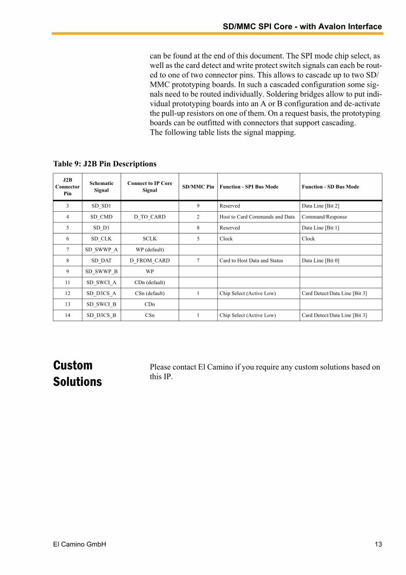
can be found at the end of this document. The SPI mode chip select, as well as the card detect and write protect switch signals can each be rout-ed to one of two connector pins. This allows to cascade up to two SD/MMC prototyping boards. In such a cascaded configuration some sig-nals need to be routed individually. Soldering bridges allow to put indi-vidual prototyping boards into an A or B configuration and de-activate the pull-up resistors on one of them. On a request basis, the prototyping boards can be outfitted with connectors that support cascading.The following table lists the signal mapping.
Custom Solutions
Please contact El Camino if you require any custom solutions based on this IP.
Table 9: J2B Pin Descriptions
J2B Connector
Pin
SchematicSignal
Connect to IP Core Signal SD/MMC Pin Function - SPI Bus Mode Function - SD Bus Mode
3 SD_SD1 9 Reserved Data Line [Bit 2]
4 SD_CMD D_TO_CARD 2 Host to Card Commands and Data Command/Response
5 SD_D1 8 Reserved Data Line [Bit 1]
6 SD_CLK SCLK 5 Clock Clock
7 SD_SWWP_A WP (default)
8 SD_DAT D_FROM_CARD 7 Card to Host Data and Status Data Line [Bit 0]
9 SD_SWWP_B WP
11 SD_SWCI_A CDn (default)
12 SD_D3CS_A CSn (default) 1 Chip Select (Active Low) Card Detect/Data Line [Bit 3]
13 SD_SWCI_B CDn
14 SD_D3CS_B CSn 1 Chip Select (Active Low) Card Detect/Data Line [Bit 3]
El Camino GmbH 13
El Camino GmbH 14
SD/MMC SPI Core - with Avalon Interface
El CaminoTraining - Engineering - Consultancy
El Camino GmbHLandshuter Str. 1D-84048 MainburgGermanyTelefone +49-8751-8787-0Telefax +49-8751-8787-10E-mail: [email protected]://www.elcamino.de
El Camino GmbH Training - Engineering - Consultancy, DIGILAB 10K10, DIGILAB picoMAX,DIGILAB 10Kx240, DIGILAB 20Kx240, DIGILAB megAPEX and other names of El Camino pro-ducts, product features and services are trademarks and/or service marks of El Camino GmbH in Ger-many and other countries. Altera, APEX, Stratix, Quartus, NIOS and other names of Altera products,product features and services are trademarks and/or service marks of Altera Corporation in the UnitedStates and other countries. Other product and company names mentioned in this document may be thetrademarks of their respective owners.No warranties: This documentation is "as is" without any express or implied warranty of any kind inclu-ding warranties of merchantability, no infringement of intellectual property or of fitness for any particu-lar purpose. In no event shall El Camino or its suppliers be liable for any damages whatsoever(including, without limitation, damages for loss of profits, business interruption or loss of information)arising out of the use of or inability to use this documentation, even if El Camino has been advised ofthe possibility of such damages. Because some jurisdictions prohibit the exclusion or limitations of lia-bility for consequential or incidental damages, some of the above limitations may not apply to you.El Camino further does not warrant the accuracy or completeness of the information, text, graphics orother items contained in this document. El Camino may make changes to these materials, or to the pro-ducts described therein, at any time without notice. El Camino makes no commitment to update this do-cument.
Copyright© 2018 El Camino GmbH. All rights reserved
Notes:


![SW Tools Solutions for DA8x - processors.wiki.ti.com€¦ · UART UART MMC/SD [at GA] ERTFS [at GA] Linux Drivers GPIO McASP GPIO McASP I2C I2C LCDC SPI SPI USB UART UART NAND EMAC](https://static.fdocuments.in/doc/165x107/5ed87c1486e3a10d342b8b79/sw-tools-solutions-for-da8x-uart-uart-mmcsd-at-ga-ertfs-at-ga-linux-drivers.jpg)