SCHOTTKY DIODE REPLACEMENT BY TRANSISTORS: SIMULATION …€¦ · SCHOTTKY DIODE REPLACEMENT BY...
5
SCHOTTKY DIODE REPLACEMENT BY TRANSISTORS: SIMULATION AND MEASURED RESULTS Martin Pospisilik Department of Computer and Communication Systems Faculty of Applied Informatics Tomas Bata University in Zlin 760 05, Zlin, Czech Republic E-mail: [email protected] KEYWORDS Model, SPICE, MOSFET, Electronic Diode, Voltage Drop, Power Dissipation ABSTRACT The software support for simulation of electrical circuits has been developed for more than sixty years. Currently, the standard tools for simulation of analogous circuits are the simulators based on the open source package Simulation Program with Integrated Circuit Emphasis generally known as SPICE (Biolek 2003). There are many different applications that provide graphical interface and extended functionalities on the basis of SPICE or, at least, using SPICE models of electronic devices. The author of this paper performed a simulation of a circuit that acts as an electronic diode in Multisim and provides a comparison of the simulation results with the results obtained from measurements on the real circuit. INTRODUCTION For the first time, Simulation Program with Integrated Circuit Emphasis (SPICE) was released in 1973 as a general-purpose, open source analog electronic circuit simulator. It was intended to check the integrity of circuit designs on the board-level and to predict the circuit behaviour in time (Vladimirescu 1994). In 2011 the development of SPICE has been named and IEEE Milestone (Bogdanowicz 2011). To process the simulation, the devices of the simulated circuit must be defined in the form of the set of parameters. These parameters can be set manually, or, obtained from the manufacturers of the devices. The simulation itself is based on numerical methods and its complexity exceeds the framework of this paper. The author has chosen the application Multisim, released by National Instruments, that employs SPICE models and algorithms, but provides graphical interface and a wide variety of device libraries. The aim was to provide a comparison of results obtained by means of simulation with the results measured on the real circuit. MOTIVATION The expansion of metal oxide field effect transistors has led to efforts to substitute conventional diodes by electronic circuit that behave in the same way as the diodes, but show considerably lower power dissipation as the voltage drop over the transistor can be eliminated to very low levels. In Fig. 1 there is a block diagram of a backup power source for the devices that use Power over Ethernet technology. This solution, that has been developed at Tomas Bata University in Zlin, enables immediate switching from the main supply to the backup one together with gentle charging of the accumulator, unlike the conventional on-line uninterruptable power sources do (Pospisilik and Neumann 2013). Figure 1: Simplified Block Diagram of the Backup Power Source for Power over Ethernet Devices When the power supply network fails, the Charge pump is activated. This results in opening of the Q1 transistor. Now the output is fed by the accumulator and the Negative voltage source is decommissioned, being blocked by the Schottky diode D1.Once the supply network starts to be active again, the Charge pump is switched off and the transistor Q1 is closed as its gate charge is distracted by the R1 resistor. The Negative voltage source is fed from the rectifier B1, delivering controlled charging voltage drop at the currents around 6 A is expected to be as high as 1 to 1.2 V, resulting in the power dissipation of up to 7.2 W. Therefore there was a need to find a simple and stable solution that would be implementable on a small area of the printed circuit board, ideally by means of surface mounted Proceedings 30th European Conference on Modelling and Simulation ©ECMS Thorsten Claus, Frank Herrmann, Michael Manitz, Oliver Rose (Editors) ISBN: 978-0-9932440-2-5 / ISBN: 978-0-9932440-3-2 (CD)
Transcript of SCHOTTKY DIODE REPLACEMENT BY TRANSISTORS: SIMULATION …€¦ · SCHOTTKY DIODE REPLACEMENT BY...
SCHOTTKY DIODE REPLACEMENT BY TRANSISTORS: SIMULATION
AND MEASURED RESULTS
Martin Pospisilik
Department of Computer and Communication Systems
Faculty of Applied Informatics
Tomas Bata University in Zlin
760 05, Zlin, Czech Republic
E-mail: [email protected]
KEYWORDS
Model, SPICE, MOSFET, Electronic Diode, Voltage
Drop, Power Dissipation
ABSTRACT
The software support for simulation of electrical circuits
has been developed for more than sixty years. Currently,
the standard tools for simulation of analogous circuits
are the simulators based on the open source package
Simulation Program with Integrated Circuit Emphasis
generally known as SPICE (Biolek 2003). There are
many different applications that provide graphical
interface and extended functionalities on the basis of
SPICE or, at least, using SPICE models of electronic
devices. The author of this paper performed a simulation
of a circuit that acts as an electronic diode in Multisim
and provides a comparison of the simulation results with
the results obtained from measurements on the real
circuit.
INTRODUCTION
For the first time, Simulation Program with Integrated
Circuit Emphasis (SPICE) was released in 1973 as a
general-purpose, open source analog electronic circuit
simulator. It was intended to check the integrity of
circuit designs on the board-level and to predict the
circuit behaviour in time (Vladimirescu 1994). In 2011
the development of SPICE has been named and IEEE
Milestone (Bogdanowicz 2011).
To process the simulation, the devices of the
simulated circuit must be defined in the form of the set
of parameters. These parameters can be set manually, or,
obtained from the manufacturers of the devices. The
simulation itself is based on numerical methods and its
complexity exceeds the framework of this paper.
The author has chosen the application Multisim,
released by National Instruments, that employs SPICE
models and algorithms, but provides graphical interface
and a wide variety of device libraries. The aim was to
provide a comparison of results obtained by means of
simulation with the results measured on the real circuit.
MOTIVATION
The expansion of metal oxide field effect transistors has
led to efforts to substitute conventional diodes by
electronic circuit that behave in the same way as the
diodes, but show considerably lower power dissipation
as the voltage drop over the transistor can be eliminated
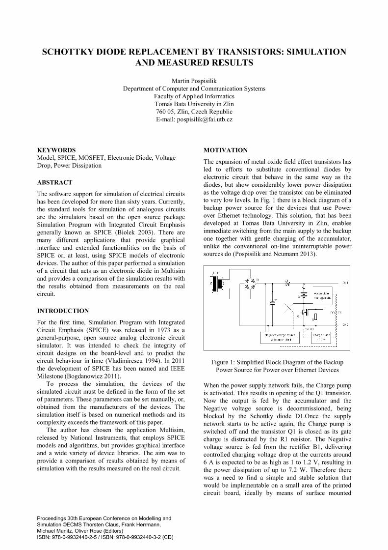
to very low levels. In Fig. 1 there is a block diagram of a
backup power source for the devices that use Power
over Ethernet technology. This solution, that has been
developed at Tomas Bata University in Zlin, enables
immediate switching from the main supply to the backup
one together with gentle charging of the accumulator,
unlike the conventional on-line uninterruptable power
sources do (Pospisilik and Neumann 2013).
Figure 1: Simplified Block Diagram of the Backup
Power Source for Power over Ethernet Devices
When the power supply network fails, the Charge pump
is activated. This results in opening of the Q1 transistor.
Now the output is fed by the accumulator and the
Negative voltage source is decommissioned, being
blocked by the Schottky diode D1.Once the supply
network starts to be active again, the Charge pump is
switched off and the transistor Q1 is closed as its gate
charge is distracted by the R1 resistor. The Negative
voltage source is fed from the rectifier B1, delivering
controlled charging voltage drop at the currents around
6 A is expected to be as high as 1 to 1.2 V, resulting in
the power dissipation of up to 7.2 W. Therefore there
was a need to find a simple and stable solution that
would be implementable on a small area of the printed
circuit board, ideally by means of surface mounted
Proceedings 30th European Conference on Modelling and Simulation ©ECMS Thorsten Claus, Frank Herrmann, Michael Manitz, Oliver Rose (Editors) ISBN: 978-0-9932440-2-5 / ISBN: 978-0-9932440-3-2 (CD)
devices, not needing any other heatsink than the copper
on the board. As the solution, a functional sample of a
circuit employing a transistor instead of the diode has
been created and its behaviour was simulated and tested.
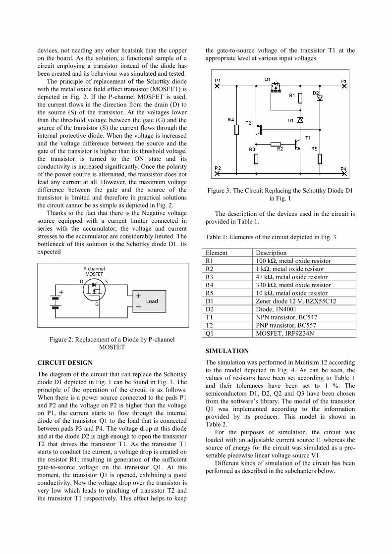
The principle of replacement of the Schottky diode
with the metal oxide field effect transistor (MOSFET) is
depicted in Fig. 2. If the P-channel MOSFET is used,
the current flows in the direction from the drain (D) to
the source (S) of the transistor. At the voltages lower
than the threshold voltage between the gate (G) and the
source of the transistor (S) the current flows through the
internal protective diode. When the voltage is increased
and the voltage difference between the source and the
gate of the transistor is higher than its threshold voltage,
the transistor is turned to the ON state and its
conductivity is increased significantly. Once the polarity
of the power source is alternated, the transistor does not
lead any current at all. However, the maximum voltage
difference between the gate and the source of the
transistor is limited and therefore in practical solutions
the circuit cannot be as simple as depicted in Fig. 2.
Thanks to the fact that there is the Negative voltage
source equipped with a current limiter connected in
series with the accumulator, the voltage and current
stresses to the accumulator are considerably limited. The
bottleneck of this solution is the Schottky diode D1. Its
expected
Figure 2: Replacement of a Diode by P-channel
MOSFET
CIRCUIT DESIGN
The diagram of the circuit that can replace the Schottky
diode D1 depicted in Fig. 1 can be found in Fig. 3. The
principle of the operation of the circuit is as follows:
When there is a power source connected to the pads P1
and P2 and the voltage on P2 is higher than the voltage
on P1, the current starts to flow through the internal
diode of the transistor Q1 to the load that is connected
between pads P3 and P4. The voltage drop at this diode
and at the diode D2 is high enough to open the transistor
T2 that drives the transistor T1. As the transistor T1
starts to conduct the current, a voltage drop is created on
the resistor R1, resulting in generation of the sufficient
gate-to-source voltage on the transistor Q1. At this
moment, the transistor Q1 is opened, exhibiting a good
conductivity. Now the voltage drop over the transistor is
very low which leads to pinching of transistor T2 and
the transistor T1 respectively. This effect helps to keep
the gate-to-source voltage of the transistor T1 at the
appropriate level at various input voltages.
Figure 3: The Circuit Replacing the Schottky Diode D1
in Fig. 1
The description of the devices used in the circuit is
provided in Table 1.
Table 1: Elements of the circuit depicted in Fig. 3
Element Description
R1 100 kΩ, metal oxide resistor
R2 1 kΩ, metal oxide resistor
R3 47 kΩ, metal oxide resistor
R4 330 kΩ, metal oxide resistor
R5 10 kΩ, metal oxide resistor
D1 Zener diode 12 V, BZX55C12
D2 Diode, 1N4001
T1 NPN transistor, BC547
T2 PNP transistor, BC557
Q1 MOSFET, IRF9Z34N
SIMULATION
The simulation was performed in Multisim 12 according
to the model depicted in Fig. 4. As can be seen, the
values of resistors have been set according to Table 1
and their tolerances have been set to 1 %. The
semiconductors D1, D2, Q2 and Q3 have been chosen
from the software’s library. The model of the transistor
Q1 was implemented according to the information
provided by its producer. This model is shown in
Table 2.
For the purposes of simulation, the circuit was
loaded with an adjustable current source I1 whereas the
source of energy for the circuit was simulated as a pre-
settable piecewise linear voltage source V1.
Different kinds of simulation of the circuit has been
performed as described in the subchapters below.
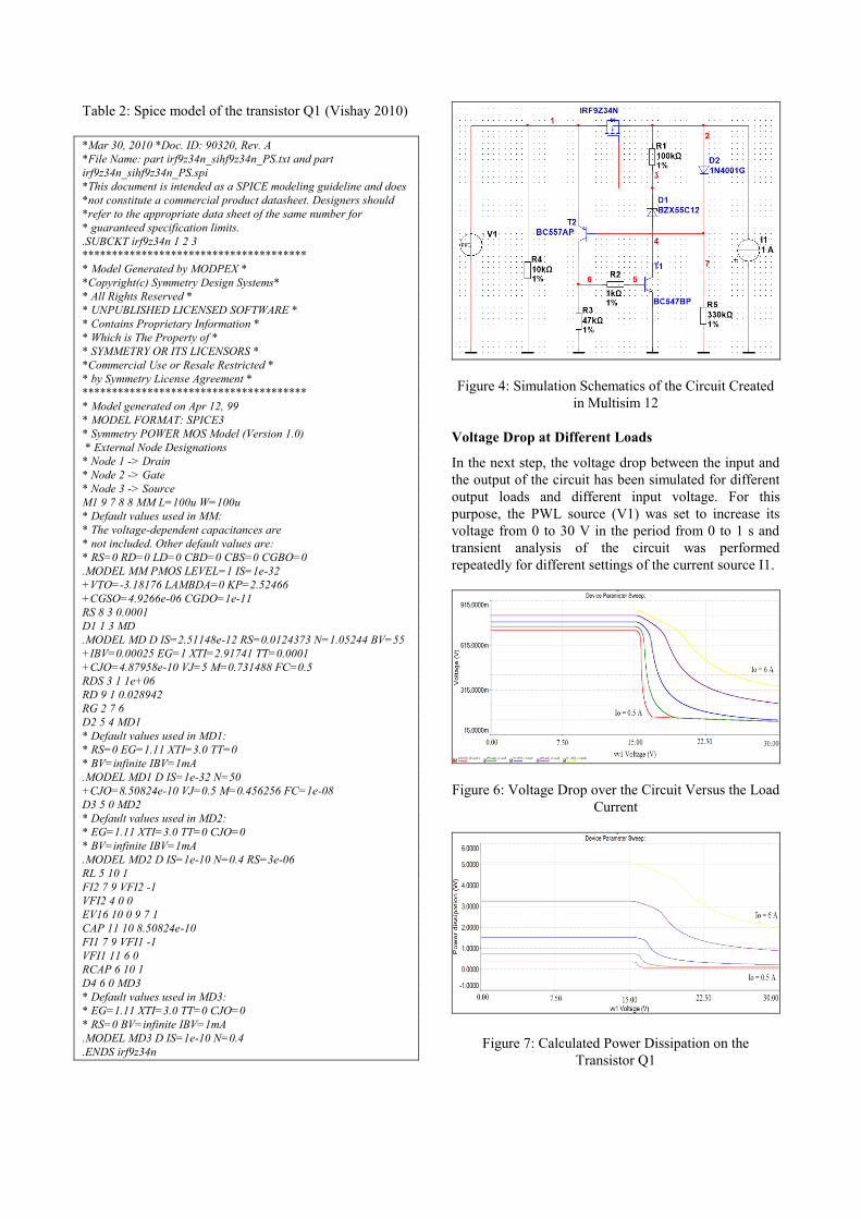
Table 2: Spice model of the transistor Q1 (Vishay 2010)
*Mar 30, 2010 *Doc. ID: 90320, Rev. A
*File Name: part irf9z34n_sihf9z34n_PS.txt and part
irf9z34n_sihf9z34n_PS.spi
*This document is intended as a SPICE modeling guideline and does
*not constitute a commercial product datasheet. Designers should
*refer to the appropriate data sheet of the same number for
* guaranteed specification limits.
.SUBCKT irf9z34n 1 2 3
**************************************
* Model Generated by MODPEX *
*Copyright(c) Symmetry Design Systems*
* All Rights Reserved *
* UNPUBLISHED LICENSED SOFTWARE *
* Contains Proprietary Information *
* Which is The Property of *
* SYMMETRY OR ITS LICENSORS *
*Commercial Use or Resale Restricted *
* by Symmetry License Agreement *
**************************************
* Model generated on Apr 12, 99
* MODEL FORMAT: SPICE3
* Symmetry POWER MOS Model (Version 1.0)
* External Node Designations
* Node 1 -> Drain
* Node 2 -> Gate
* Node 3 -> Source
M1 9 7 8 8 MM L=100u W=100u
* Default values used in MM:
* The voltage-dependent capacitances are
* not included. Other default values are:
* RS=0 RD=0 LD=0 CBD=0 CBS=0 CGBO=0
.MODEL MM PMOS LEVEL=1 IS=1e-32
+VTO=-3.18176 LAMBDA=0 KP=2.52466
+CGSO=4.9266e-06 CGDO=1e-11
RS 8 3 0.0001
D1 1 3 MD
.MODEL MD D IS=2.51148e-12 RS=0.0124373 N=1.05244 BV=55
+IBV=0.00025 EG=1 XTI=2.91741 TT=0.0001
+CJO=4.87958e-10 VJ=5 M=0.731488 FC=0.5
RDS 3 1 1e+06
RD 9 1 0.028942
RG 2 7 6
D2 5 4 MD1
* Default values used in MD1:
* RS=0 EG=1.11 XTI=3.0 TT=0
* BV=infinite IBV=1mA
.MODEL MD1 D IS=1e-32 N=50
+CJO=8.50824e-10 VJ=0.5 M=0.456256 FC=1e-08
D3 5 0 MD2
* Default values used in MD2:
* EG=1.11 XTI=3.0 TT=0 CJO=0
* BV=infinite IBV=1mA
.MODEL MD2 D IS=1e-10 N=0.4 RS=3e-06
RL 5 10 1
FI2 7 9 VFI2 -1
VFI2 4 0 0
EV16 10 0 9 7 1
CAP 11 10 8.50824e-10
FI1 7 9 VFI1 -1
VFI1 11 6 0
RCAP 6 10 1
D4 6 0 MD3
* Default values used in MD3:
* EG=1.11 XTI=3.0 TT=0 CJO=0
* RS=0 BV=infinite IBV=1mA
.MODEL MD3 D IS=1e-10 N=0.4
.ENDS irf9z34n
Figure 4: Simulation Schematics of the Circuit Created
in Multisim 12
Voltage Drop at Different Loads
In the next step, the voltage drop between the input and
the output of the circuit has been simulated for different
output loads and different input voltage. For this
purpose, the PWL source (V1) was set to increase its
voltage from 0 to 30 V in the period from 0 to 1 s and
transient analysis of the circuit was performed
repeatedly for different settings of the current source I1.
Figure 6: Voltage Drop over the Circuit Versus the Load
Current
Figure 7: Calculated Power Dissipation on the
Transistor Q1
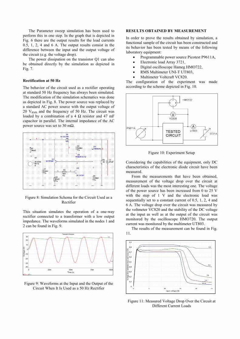
The Parameter sweep simulation has been used to
perform this in one step. In the graph that is depicted in
Fig. 6 there are the output results for the load currents
0.5, 1, 2, 4 and 6 A. The output results consist in the
difference between the input and the output voltage of
the circuit (e.g. the voltage drop).
The power dissipation on the transistor Q1 can also
be obtained directly by the simulation as depicted in
Fig. 7.
Rectification at 50 Hz
The behavior of the circuit used as a rectifier operating
at standard 50 Hz frequency has always been simulated.
The modification of the simulation schematics was done
as depicted in Fig. 8. The power source was replaced by
a standard AC power source with the output voltage of
20 VRMS and the frequency of 50 Hz. The circuit was
loaded by a combination of a 4 Ω resistor and 47 mF
capacitor in parallel. The internal impedance of the AC
power source was set to 30 mΩ.
Figure 8: Simulation Schema for the Circuit Used as a
Rectifier
This situation simulates the operation of a one-way
rectifier connected to a transformer with a low output
impedance. The waveforms simulated in the nodes 1 and
2 can be found in Fig. 9.
Figure 9: Waveforms at the Input and the Output of the
Circuit When It Is Used as a 50 Hz Rectifier
RESULTS OBTAINED BY MEASUREMENT
In order to prove the results obtained by simulation, a
functional sample of the circuit has been constructed and
its behavior has been tested by means of the following
laboratory equipment:
Programmable power source Picotest P9611A,
Electronic load Array 3721,
Digital oscilloscope Hameg HMO722,
RMS Multimeter UNI-T UT803,
Multimeter Voltcraft VC820.
The configuration of the experiment was made
according to the scheme depicted in Fig. 10.
Figure 10: Experiment Setup
Considering the capabilities of the equipment, only DC
characteristics of the electronic diode circuit have been
measured.
From the measurements that have been obtained,
measurement of the voltage drop over the circuit at
different loads was the most interesting one. The voltage
of the power source has been increased from 0 to 25 V
with the step of 1 V and the electronic load was
sequentially set to a constant current of 0.5, 1, 2, 4 and
6 A. The voltage drop over the circuit was measured by
the voltmeter VC820 and the stability of the DC voltage
at the input as well as at the output of the circuit was
monitored by the oscilloscope HMO720. The output
current was monitored by the multimeter UT803.
The results of the measurement can be found in Fig.
11.
Figure 11: Measured Voltage Drop Over the Circuit at
Different Current Loads

The findings resulting from the experimental
measurement can be compared to the results of
simulation of the same operating conditions of the
circuit that are depicted in Fig. 6. For low currents the
measured results correspond to the results obtained by
the simulation. However, at higher currents the results
obtained by the simulation were not correct. It is
expected, that the increased voltage drop, obtained by
the real experiment, has been partially caused by the
resistance of the connecting wires as well as by the
resistance of the PCB traces. At the current of 6 A and
the input voltage of 22.5 V, considering the voltage drop
over the current, the difference between the simulation
and the measurement was as high as 0.3 V, which
corresponds to the traces’ resistance of about 50 mΩ.
CONCLUSIONS
In this paper the construction of the circuit that replaces
a conventional Schottky diode is described together with
the results of simulations that were made in order to
verify the circuit’s design before it was constructed as
well as with the results obtained by measurement on the
functional sample of this circuit. It was proven that the
circuit operates correctly and the achieved results were
close to the simulated behavior of the circuit with the
exception of high current loads. When the circuit was
loaded with high currents, the voltage drop over it was
considerably higher than simulated.
Acknowledgements
This work was supported by the Ministry of Education,
Youth and Sports of the Czech Republic within the
National Sustainability Programme project No. LO1303
(MSMT-7778/2014).
REFERENCES
Biolek, D. 2003. Solving of electrical circuits [Resime
elektronicke obvody]. BEN – Technicka literatura. ISBN
80-7300-125-X.
Vladimirescu, A. 1994. The SPICE book. John Willey & Sons.
ISBN 978-0471609261.
Bogdanowicz, A. 2011. “SPICE Circuit Simulator Named
IEEE Milestone”. The institute. IEEE.
Pospisilik, M., Neumann, P. 2013. “Improved Design of the
Uninterruptable Power Supply Unit for Powering of
Network Devices”. In 19th IEEE International Symposium
on Design and Diagnostics of Electrical Circuits. Karlovy
Vary, Czech Republic. ISBN 978-1-4673-6133-0.
Vishay. 2010. IRF9Z34 SPICE model. Online:
http://www.vishay.com/docs/90320/sihf9z34.lib
AUTHOR BIOGRAPHY
MARTIN POSPISILIK was born in
Přílepy, Czech Republic. He reached his
master degree at the Czech Technical
University in Prague in the field of
Microelectronics in 2008. Since 2013, after
finishing his Ph.D. work focused on a construction of
the Autonomous monitoring system, he became an
assistant professor at the Tomas Bata University in Zlin,
focused on communication systems and electromagnetic
compatibility of electronic components. His e-mail is: [email protected]