scan test by sanjay d dhandare
19
SANJAY . D . DHNDARE 19/02/22 1 ME(E&TC engg.),DYPSOE,Lohegaon,Pune
-
Upload
sanjay-dhandare -
Category
Engineering
-
view
163 -
download
4
Transcript of scan test by sanjay d dhandare

SANJAY . D . DHNDARE
03/05/23 1ME(E&TC engg.),DYPSOE,Lohegaon,Pune

CONTENT :
Introduction Brief history Need Boundary Scan Test Terminology used Working What is four wire test ?
03/05/23 2ME(E&TC engg.),DYPSOE,Lohegaon,Pune

Cont....
BST cell and its VHDL code
BST register
TAP controller
Signal specification
Timing diagram
Conclusion
03/05/23 ME(E&TC engg.),DYPSOE,Lohegaon,Pune 3

INTRODUCTION
What is scan test ? The method in which testing of boards , separate
components and ASIC is carried out in a efficient way is called as scan test.
It is also known as Boundary Scan Test (BST).
03/05/23 4ME(E&TC engg.),DYPSOE,Lohegaon,Pune

BRIEF HISTORY
1985 : JETAG studied a board testing 1986 : JETAG became JTEG 1990 : ANSI provide 2.0 standard 1994 : JTAG formed 2.0 standard with
1149.1 IEEE standard 1994 : New standard for test port and BST
i.e.1149.1b From 1994 IEEE standard still referred as a
JTAG standard
03/05/23 ME(E&TC engg.),DYPSOE,Lohegaon,Pune 5

NEED Existing technology i.e. Bed-of-nail had limited
specification . Difficult to test the IC with closer pin spacing. Testing speed is generally low . Only one component testing is carried out at
one time . Separation below 0.1mm or 100 mm with 200
or more pins is not possible in bed-of-nail testing .
Need standard System Test Port and Bus.03/05/23 6ME(E&TC engg.),DYPSOE,Lohegaon,Pune

BOUNDARY SCAN TEST
03/05/23 7ME(E&TC engg.),DYPSOE,Lohegaon,Pune
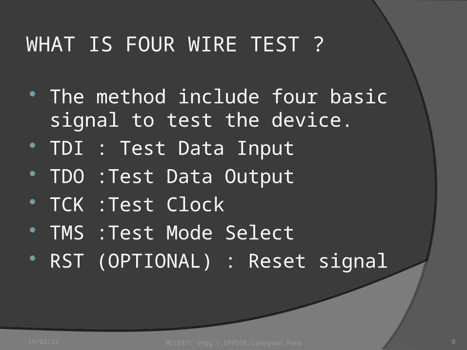
WHAT IS FOUR WIRE TEST ?
The method include four basic signal to test the device.
TDI : Test Data Input TDO :Test Data Output TCK :Test Clock TMS :Test Mode Select RST (OPTIONAL) : Reset signal
03/05/23 ME(E&TC engg.),DYPSOE,Lohegaon,Pune 8

TERMINOLOGY USED
03/05/23 ME(E&TC engg.),DYPSOE,Lohegaon,Pune 9

BST CELL AND ITS VHDL CODE
03/05/23 ME(E&TC engg.),DYPSOE,Lohegaon,Pune 10

BST REGISTER
03/05/23 ME(E&TC engg.),DYPSOE,Lohegaon,Pune 11

TAP CONTROLLER STATE DIAGRAM
03/05/23 ME(E&TC engg.),DYPSOE,Lohegaon,Pune 12

TIMING DIAGRAM
03/05/23 ME(E&TC engg.),DYPSOE,Lohegaon,Pune 13

POWER ON RESET FOR TAP
03/05/23 ME(E&TC engg.),DYPSOE,Lohegaon,Pune 14

BST INSTRUCTION
SAMPLE /PRELOAD : To get snapshot of chip output signal i.e. put data on a chip to be test .
EXTEST : To test off-chip circuits INTEST : To test on-chip circuits CLAMP : Forces component output to be
driven by BSR INCODE :To get the ID of device to be
check
03/05/23 ME(E&TC engg.),DYPSOE,Lohegaon,Pune 15

Cont... USER CODE :To get the ID of user programmable
device under test
HIGH Z: To bring the output all components at
high impedance state
It will avoid damage of components
Need to reset the controller or board when goes into
high impedance state
03/05/23 ME(E&TC engg.),DYPSOE,Lohegaon,Pune 16

CONCLUSION
From a given discussion we can conclude that it is not possible to test printed circuit boards with bed-of-nails tester to test multi-chip modules at all without BST hence it is an important tool to test the circuitry .
03/05/23 17ME(E&TC engg.),DYPSOE,Lohegaon,Pune

REFERENCES
Digital system testing and testable design by
M.Abramovici .
Agrawal.V. K. Multiple fault testing of large circuits
IEEE trans.vol c-30,no.11 pp 855 865.
Introduction to testing and BIST by Breuer .M .A. And
A. D. Friedman.
03/05/23 18ME(E&TC engg.),DYPSOE,Lohegaon,Pune

.
Thank you ...
03/05/23 19ME(E&TC engg.),DYPSOE,Lohegaon,Pune