Scaling and Beyond for Logic and Memories. Which … and Beyond for Logic and Memories. Which...
64
Scaling and Beyond for Logic and Memories. Scaling and Beyond for Logic and Memories. Which perspectives? Which perspectives? September 26 th , 2012 Minatec, Grenoble - France Hiroshi Iwai and Barbara de Salvo Frontier Research Center, Tokyo Institute of Technology CEA-LETI ISCDG 2012, Short Course 1
-
Upload
nguyenkhanh -
Category
Documents
-
view
223 -
download
3
Transcript of Scaling and Beyond for Logic and Memories. Which … and Beyond for Logic and Memories. Which...

Scaling and Beyond for Logic and Memories. Scaling and Beyond for Logic and Memories. Which perspectives?Which perspectives?
September 26th, 2012 Minatec, Grenoble - France
Hiroshi Iwai and Barbara de Salvo
Frontier Research Center, Tokyo Institute of TechnologyCEA-LETI
ISCDG 2012, Short Course
1

Scaling and Beyond for LogicScaling and Beyond for Logic
September 26th, 2012 Minatec, Grenoble - France
ISCDG 2012, Short Course
2
Part IPart I

More Moore approach
Advance Si-based CMOS devices and technologies
Technology benchmark
Challenges
Alternative channel material devicesTechnology benchmark
III-V, Ge-based devices
Emerging technologies(Tunnel FET, Junctionless FET, Carbon-based FET, MEMS,Spin-based Logic)
Conclusions
OutlineOutline
3

More Moore approach
Advance Si-based CMOS devices and technologies
Technology benchmark
Challenges
Alternative channel material devicesTechnology benchmark
III-V, Ge-based devices
Emerging technologies(Tunnel FET, Junctionless FET, Carbon-based FET, MEMS,Spin-based Logic)
Conclusions
OutlineOutline
4

Planar to MultiPlanar to Multi--gate, New highgate, New high--kk
5
Fin Tri-gate Ω-gate All-around
G G G
G
G
Off-leakage is the obstacle for downsizing.
1. New channelstructure
Solutions
2. Thinning gate oxide New high-k

More Moore to More More MooreMore Moore to More More Moore
65nm 45nm 32nm
Technology node
M. Bohr, pp.1, IEDM2011 (Intel)P. Packan, pp.659, IEDM2009 (Intel)C. Auth et al., pp.131, VLSI2012 (Intel)T. B. Hook, pp.115, IEDM2011 (IBM)S. Bangsaruntip et al., pp.297, IEDM2009 (IBM)
Lg 35nm Lg 30nm
Main stream(Fin,Tri, Nanowire)
22nm 15nm, 11nm, 8nm, 5nm, 3nm
Alternative
Alternative (III-V/Ge) Channel FinFET
Emerging Devices 6
Tri-Gate
Now Future
Si channelSi
Others
(ETSOI)
Planar
Si is still main stream for future !! ET: Extremely Thin
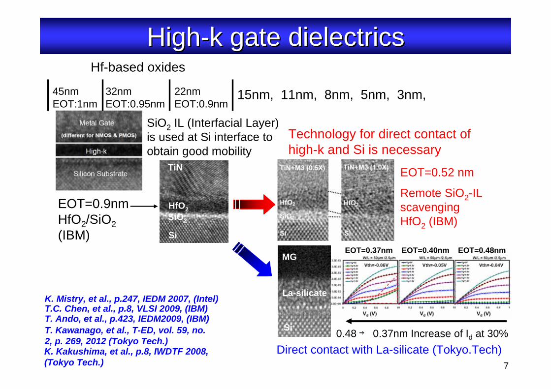
HighHigh--k gate dielectricsk gate dielectrics
SiO2 IL (Interfacial Layer) is used at Si interface to obtain good mobility
Technology for direct contact of high-k and Si is necessary
Remote SiO2-IL scavengingHfO2 (IBM)
EOT=0.52 nm
Si
La-silicate
MG
Direct contact with La-silicate (Tokyo.Tech)
T. Ando, et al., p.423, IEDM2009, (IBM) T. Kawanago, et al., T-ED, vol. 59, no. 2, p. 269, 2012 (Tokyo Tech.)
K. Mistry, et al., p.247, IEDM 2007, (Intel)
TiN
HfO2
Si
SiO2
EOT=0.9nmHfO2/SiO2(IBM)
T.C. Chen, et al., p.8, VLSI 2009, (IBM)
Hf-based oxides
45nmEOT:1nm
32nmEOT:0.95nm
22nmEOT:0.9nm
15nm, 11nm, 8nm, 5nm, 3nm,
K. Kakushima, et al., p.8, IWDTF 2008, (Tokyo Tech.)
EOT=0.37nm EOT=0.40nm EOT=0.48nm
0.48 → 0.37nm Increase of Id at 30%
7
[1] C. Auth et al., pp.131, VLSI2012 (Intel).[2] K. Mistry et al., pp.247, IEDM2007 (Intel).[3] H.-J. Cho et al., pp.350, IEDM2011 (Samsung).[4] S. Saitoh et al., pp.11, VLSI2012 (Toshiba).[5] S. Bangsaruntip et al., pp.297, IEDM2009 (IBM).
[6] T. Yamashita et al., pp.14, VLSI2011 (IBM).[7] A. Khakifirooz et al., pp.117, VLSI2012 (IBM).
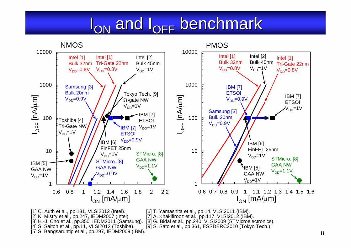
IIONON and Iand IOFFOFF benchmarkbenchmark
[8] G. Bidal et al., pp.240, VLSI2009 (STMicroelectronics).
1
10
100
1000
10000
0.6 0.7 0.8 0.9 1 1.1 1.2 1.3 1.4 1.5 1.6ION [mA/µm]
I OFF
[nA
/µm
]
PMOSIntel [1]Bulk 32nmVDD=0.8V
Intel [1]Tri-Gate 22nmVDD=0.8V
Intel [2]Bulk 45nmVDD=1V
IBM [7]ETSOIVDD=1VSamsung [3]
Bulk 20nmVDD=0.9V
IBM [5]GAA NWVDD=1V
IBM [6]FinFET 25nmVDD=1V
IBM [7]ETSOIVDD=0.9V
STMicro. [8]GAA NWVDD=1.1V
1
10
100
1000
10000
0.6 0.8 1 1.2 1.4 1.6 1.8 2 2.2ION [mA/µm]
I OFF
[nA
/µm
]NMOS
Intel [1]Bulk 32nmVDD=0.8V
Intel [1]Tri-Gate 22nmVDD=0.8V
Intel [2]Bulk 45nmVDD=1V
Toshiba [4]Tri-Gate NWVDD=1V
Samsung [3]Bulk 20nmVDD=0.9V
IBM [5]GAA NWVDD=1V
IBM [6]FinFET 25nmVDD=1V
IBM [7]ETSOIVDD=0.9V
IBM [7]ETSOIVDD=1V
STMicro. [8]GAA NWVDD=0.9V
STMicro. [8]GAA NWVDD=1.1V
Tokyo Tech. [9]Ω-gate NWVDD=1V
[9] S. Sato et al., pp.361, ESSDERC2010 (Tokyo Tech.)8

C. Auth et al., pp.131, VLSI2012 (Intel).
K. Mistry et al., pp.247, IEDM2007 (Intel).P. Packan et al., pp.659, IEDM2009 (Intel).
Comparison with ITRSComparison with ITRS
0
0.2
0.4
0.6
0.8
1
1.2
1.4
2006 2008 2010 2012 2014 2016 2018 20200
0.2
0.4
0.6
0.8
1
1.2
1.4
YearV
DD
(V)
VDD
Vth
ITRS2007~2011
Intel
45nm 32nm
22nm
Intel45nm32nm
22nm
Multi-GateBulk Planar
Vth (V
)
0
5
10
15
20
25
30
35
40
2006 2008 2010 2012 2014 2016 2018 20200.4
0.6
0.8
1
1.2
1.4
1.6
1.8
2
Year
L g(n
m)
EO
T (nm)
Intel45nm32nm 22nm
ITRS2007~2011
Intel
45nm 32nm
22nmMulti-Gate
Bulk PlanarITRS2007
EOT
LgITRS2009~2011
9

Benchmark of device characteristicsBenchmark of device characteristics
<80
56/9
2.05/1.5
1.1
~0.5
-
HfZrO2
22/30 (nFET/pFET)
GAA NW
STMicro. (VLSI2008)
85
65/105
0.83/0.95
1
0.3~0.4
1.5
Hf-based
35/25 (nFET/pFET)
GAA NW
IBM (IEDM2009)
Intel(IEDM2007, 2009)
Intel (VLSI2012)
Toshiba (VLSI2012)
IBM (VLSI2012)
Samsung (IEDM2012)
Tokyo Tech (ESSDERC2010)
StructureBulk Planar Tri-Gate
22nm Tri-Gate NW ETSOI Bulk Planar Ω-gate NW45nm 32nm
Lg (nm) 35 30 30 14 22 20 65
Gate Dielectrics Hf-based Hf-based SiO2 HfO2 HfO2 ? SiO2
EOT (nm) 1 0.95 0.9 3 ~1 - 3
Vth (V) ~0.4 ~0.3 ~0.2 -0.15 (nFET) 0.3~0.4 ~0.3 -0.2 (nFET)
VDD (V) 1 1 0.8 1 1 0.9 1
ION (mA/um) nFET/pFET 1.36/1.07 1.53/1.23 1.26/1.1 0.83 (nFET) 1.65/1.25 1.2/1.05 1.32 (nFET)
DIBL (mV/V)
nFET/pFET~150 ~200 46/50 <50 75/130 104/115 62
SS (mV/dec) - ~100 ~70 <80 <90 87 70<80
56/9
2.05/1.5
1.1
~0.5
-
HfZrO2
22/30 (nFET/pFET)
GAA NW
STMicro. (VLSI2008)
85
65/105
0.83/0.95
1
0.3~0.4
1.5
Hf-based
35/25 (nFET/pFET)
GAA NW
IBM (IEDM2009)
Intel(IEDM2007, 2009)
Intel (VLSI2012)
Toshiba (VLSI2012)
IBM (VLSI2012)
Samsung (IEDM2012)
Tokyo Tech (ESSDERC2010)
StructureBulk Planar Tri-Gate
22nm Tri-Gate NW ETSOI Bulk Planar Ω-gate NW45nm 32nm
Lg (nm) 35 30 30 14 22 20 65
Gate Dielectrics Hf-based Hf-based SiO2 HfO2 HfO2 ? SiO2
EOT (nm) 1 0.95 0.9 3 ~1 - 3
Vth (V) ~0.4 ~0.3 ~0.2 -0.15 (nFET) 0.3~0.4 ~0.3 -0.2 (nFET)
VDD (V) 1 1 0.8 1 1 0.9 1
ION (mA/um) nFET/pFET 1.36/1.07 1.53/1.23 1.26/1.1 0.83 (nFET) 1.65/1.25 1.2/1.05 1.32 (nFET)
DIBL (mV/V)
nFET/pFET~150 ~200 46/50 <50 75/130 104/115 62
SS (mV/dec) - ~100 ~70 <80 <90 87 70
10

More Moore approach
Advance Si-based CMOS devices and technologies
Technology benchmark
Challenges
Alternative channel material devicesTechnology benchmark
III-V, Ge-based devices
Emerging technologies(Tunnel FET, Junctionless FET, Carbon-based FET, MEMS,Spin-based Logic)
Conclusions
OutlineOutline
11
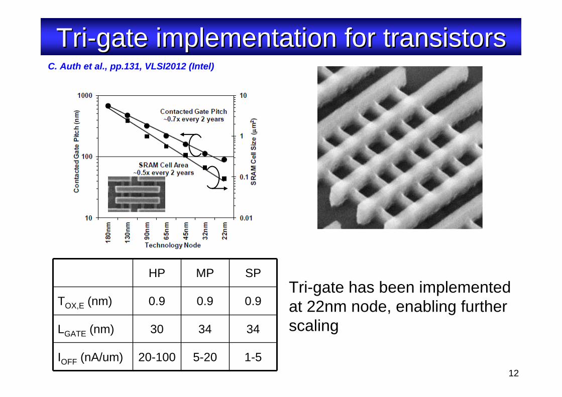
HP MP SP
TOX,E (nm) 0.9 0.9 0.9
LGATE (nm) 30 34 34
IOFF (nA/um) 20-100 5-20 1-5
Tri-gate has been implemented at 22nm node, enabling further scaling
C. Auth et al., pp.131, VLSI2012 (Intel)
TriTri--gate implementation for transistors gate implementation for transistors
12
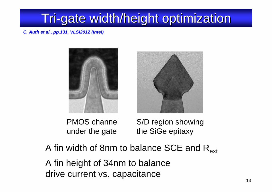
PMOS channel under the gate
S/D region showing the SiGe epitaxy
A fin width of 8nm to balance SCE and Rext
A fin height of 34nm to balance drive current vs. capacitance
C. Auth et al., pp.131, VLSI2012 (Intel)
TriTri--gate width/height optimizationgate width/height optimization
13
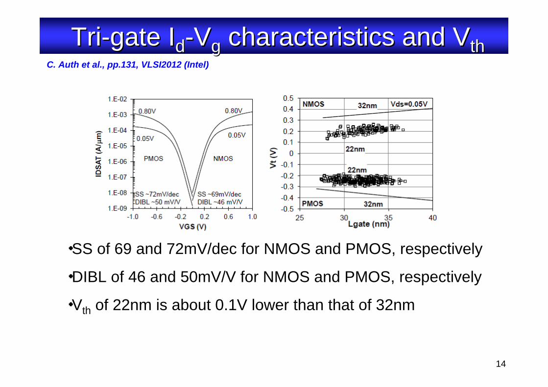
C. Auth et al., pp.131, VLSI2012 (Intel)
TriTri--gate Igate Idd--VVgg characteristics and Vcharacteristics and Vthth
・SS of 69 and 72mV/dec for NMOS and PMOS, respectively
・DIBL of 46 and 50mV/V for NMOS and PMOS, respectively
・Vth of 22nm is about 0.1V lower than that of 32nm
14

NMOS PMOS
C. Auth et al., pp.131, VLSI2012 (Intel)
TriTri--gate Igate IONON and Iand IOFFOFF characteristicscharacteristics
HP MP SP
ION (mA/um) NMOS/PMOS 1.26/1.1 1.07/0.95 0.88/0.78
IOFF (nA/um) 20-100 5-20 1-5
ION/IOFF ~105 ~106 ~106
ION/IOFF of 105~106
15

S. Saitoh et al., pp.11, VLSI2012 (Toshiba)
・Lg = 14nm Tri-Gate NW
・High SCE immunity at Lg of 14nm
・Vth tuning by applying Vsub at thin BOX of 20nm
TriTri--Gate NanowireGate Nanowire
Vsub
16

H.-J. Cho et al., pp.350, IEDM2011 (Samsung)
・Lg = 20nm bulk planar CMOS
・Gate last integration
・In-situ doped S/D for better SCE
Bulk PlanarBulk Planar
17
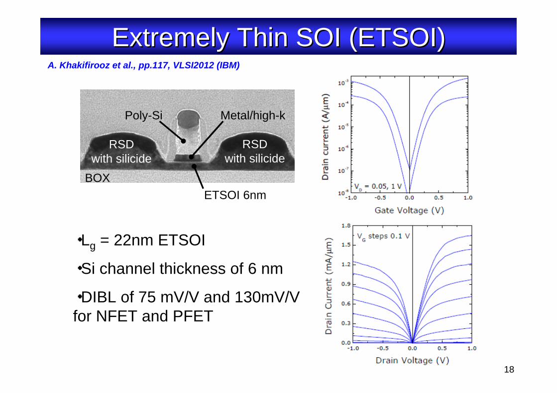
A. Khakifirooz et al., pp.117, VLSI2012 (IBM)
・Lg = 22nm ETSOI
・Si channel thickness of 6 nm
・DIBL of 75 mV/V and 130mV/V for NFET and PFET
Extremely Thin SOI (ETSOI)Extremely Thin SOI (ETSOI)
RSDwith silicide
RSDwith silicide
ETSOI 6nmBOX
Poly-Si Metal/high-k
18

S. Bangsaruntip et al., pp.297, IEDM2009 (IBM)
・Lg = 25~35nm GAA NW
・Hydrogen anneal provide smooth channel surface
・Competitive with conventional CMOS technologies
・Scaling the dimensions of NW leads to suppressed SCE
Gate All Around Nanowire (GAA NW)Gate All Around Nanowire (GAA NW)
19

G. Bidal et al., pp.240, VLSI2009 (STMicroelectronics)
SiNHMTop Gate
Bottom Gate
Channel
NiPtSi
・Gate all around structure
・Lg of 22~30nm
・High drive currents by special stress and channel orientation design
Gate All Around Nanowire (GAA NW)Gate All Around Nanowire (GAA NW)
20
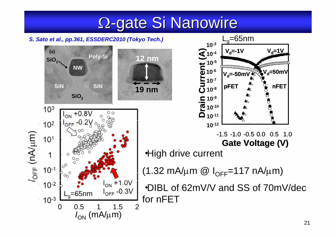
ΩΩ--gate Si Nanowiregate Si NanowireS. Sato et al., pp.361, ESSDERC2010 (Tokyo Tech.)
19 nm
12 nm
1.E-12
1.E-11
1.E-10
1.E-09
1.E-08
1.E-07
1.E-06
1.E-05
1.E-04
1.E-03
-1.5 -1.0 -0.5 0.0 0.5 1.010-12
Gate Voltage (V)
pFET nFET
10-11
10-10
10-9
10-8
10-7
10-6
10-5
10-4
10-3
Dra
in C
urre
nt (A
)
Vd=-50mV
Vd=-1V
Vd=50mV
Vd=1V
1.E-12
1.E-11
1.E-10
1.E-09
1.E-08
1.E-07
1.E-06
1.E-05
1.E-04
1.E-03
-1.5 -1.0 -0.5 0.0 0.5 1.010-12
Gate Voltage (V)
pFET nFET
10-11
10-10
10-9
10-8
10-7
10-6
10-5
10-4
10-3
Dra
in C
urre
nt (A
)
Vd=-50mV
Vd=-1V
Vd=50mV
Vd=1V
0 0.5 1 1.5 2ION (mA/µm)
Lg=65nm
0 0.5 1 1.5 2ION (mA/µm)
Lg=65nm
Lg=65nm
Poly-Si
SiO2
SiNSiN
SiO2
NW
・High drive current
(1.32 mA/µm @ IOFF=117 nA/µm)
・DIBL of 62mV/V and SS of 70mV/dec for nFET
21

More Moore approach
Advance Si-based CMOS devices and technologies
Technology benchmark
Challenges
Alternative channel material devicesTechnology benchmark
III-V, Ge-based devices
Emerging technologies(Tunnel FET, Junctionless FET, Carbon-based FET, MEMS,Spin-based Logic)
Conclusions
OutlineOutline
22

S. Bangsaruntip et al., pp.297, IEDM2009 (IBM), K. Tachi et al., pp.313, IEDM2009 (CEA-LETI)
Decreasing the diameter of NW
Problems in MultiProblems in Multi--gategate
Improvedshort-channel control
Severe mobility degradation
23

K. Uchida et al., pp.47, IEDM2002 (Toshiba)
Problems in SOIProblems in SOI
Mobility is also decreased with decreasing the Si thickness of SOI transistor similar to the NW transistor.
24
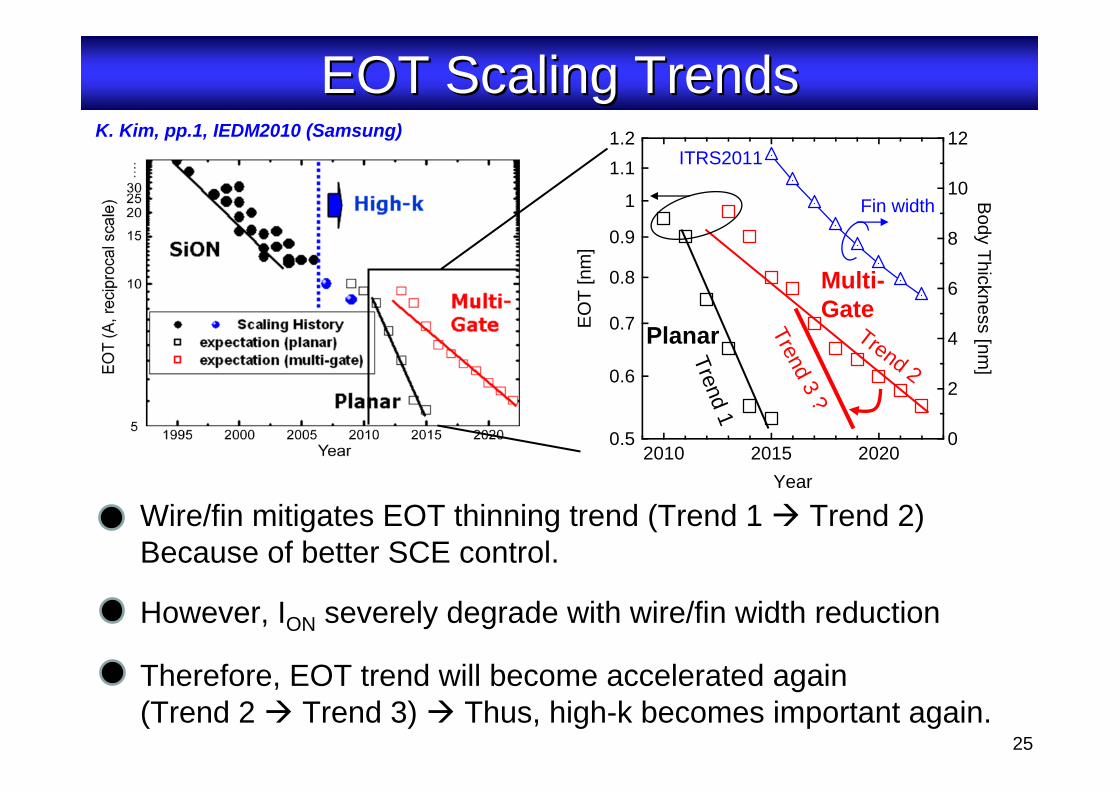
K. Kim, pp.1, IEDM2010 (Samsung) 1.21.1
1
0.9
0.8
0.7
0.6
0.5
EO
T [n
m]
202020152010Year
12
10
8
6
4
2
0
Body Thickness [nm
]
Multi-Gate
Planar
ITRS2011
Fin width
Trend 1
Trend 2Trend 3 ?
EOT Scaling TrendsEOT Scaling Trends
Wire/fin mitigates EOT thinning trend (Trend 1 Trend 2)Because of better SCE control.
However, ION severely degrade with wire/fin width reduction
Therefore, EOT trend will become accelerated again(Trend 2 Trend 3) Thus, high-k becomes important again.
25

Advantages of metal S/D- atomically abrupt junction- low parasitic resistance- reduced channel dopantconcentrationIssues in metal S/D- two different φB for p/n-ch FETs- underlap/overlap to the gate- narrow process temperature window
L. Hutin, pp.45, IEDM2009 (CEA-LETI)
S D
BOX
Dopant Segregationlayer
Si
Metal S/D is considered for alternativechannel material such as InGaAs and Ge
S.-H. Kim, IEDM (2010) 596
Ni is used both onInGaAs and Ge to
form alloy.
K. Ikeda, VLSI (2012) 165
Metal S/DMetal S/D
26
More Moore approach
Advance Si-based CMOS devices and technologies
Technology benchmark
Challenges
Alternative channel material devicesTechnology benchmark
III-V, Ge-based devices
Emerging technologies(Tunnel FET, Junctionless FET, Carbon-based FET, MEMS,Spin-based Logic)
Conclusions
OutlineOutline
27

Ge,IIIGe,III--V bulk properties V bulk properties
S. Takagi., IEDM2011, Short course (Tokyo Uni) 28
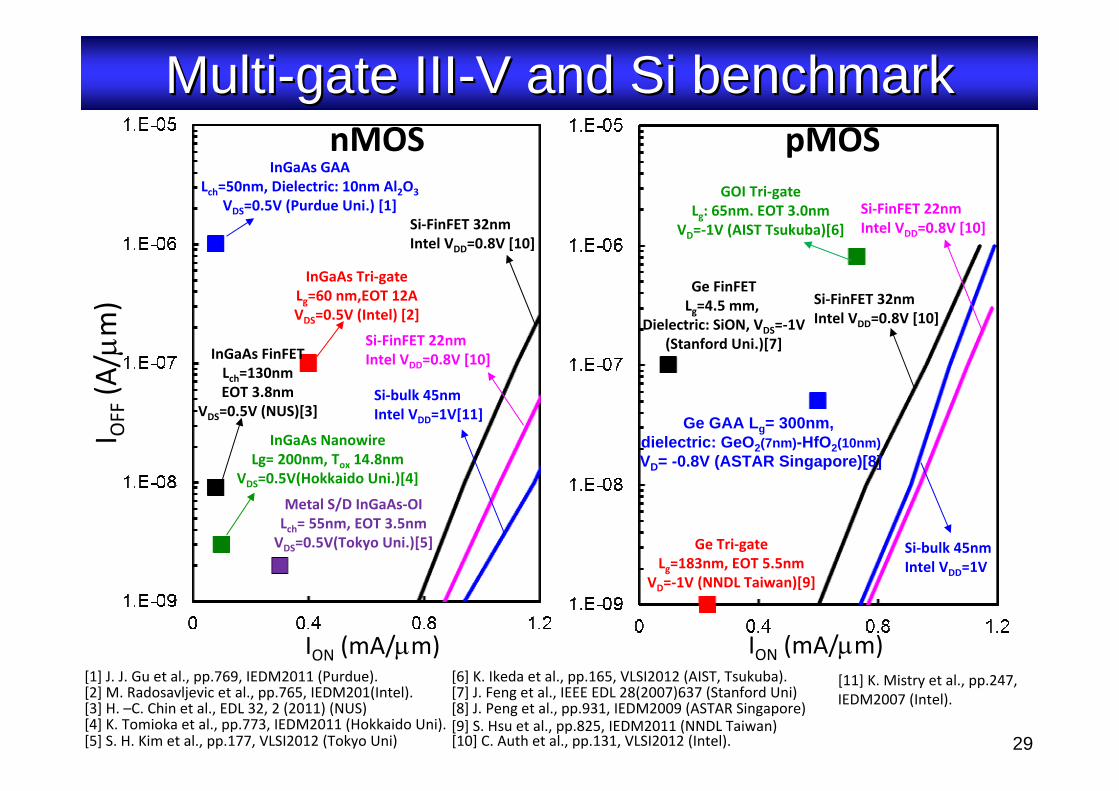
Metal S/D InGaAs‐OILch= 55nm, EOT 3.5nmVDS=0.5V(Tokyo Uni.)[5]
InGaAs NanowireLg= 200nm, Tox 14.8nm
VDS=0.5V(Hokkaido Uni.)[4]
InGaAs FinFETLch=130nmEOT 3.8nm
VDS=0.5V (NUS)[3]
InGaAs Tri‐gateLg=60 nm,EOT 12AVDS=0.5V (Intel) [2]
InGaAs GAALch=50nm, Dielectric: 10nm Al2O3
VDS=0.5V (Purdue Uni.) [1]
Ge Tri‐gateLg=183nm, EOT 5.5nm
VD=‐1V (NNDL Taiwan)[9]
Ge GAA Lg= 300nm, dielectric: GeO2(7nm)-HfO2(10nm)VD= -0.8V (ASTAR Singapore)[8]
Ge FinFETLg=4.5 mm,
Dielectric: SiON, VDS=‐1V(Stanford Uni.)[7]
GOI Tri‐gateLg: 65nm. EOT 3.0nm
VD=‐1V (AIST Tsukuba)[6]
Si‐bulk 45nmIntel VDD=1V
I OFF(A/µm)
ION (mA/µm)
nMOS pMOS
ION (mA/µm)[1] J. J. Gu et al., pp.769, IEDM2011 (Purdue).[2] M. Radosavljevic et al., pp.765, IEDM201(Intel).[3] H. –C. Chin et al., EDL 32, 2 (2011) (NUS)[4] K. Tomioka et al., pp.773, IEDM2011 (Hokkaido Uni).
[6] K. Ikeda et al., pp.165, VLSI2012 (AIST, Tsukuba).[7] J. Feng et al., IEEE EDL 28(2007)637 (Stanford Uni)[8] J. Peng et al., pp.931, IEDM2009 (ASTAR Singapore)[9] S. Hsu et al., pp.825, IEDM2011 (NNDL Taiwan)
[5] S. H. Kim et al., pp.177, VLSI2012 (Tokyo Uni)
Si‐bulk 45nmIntel VDD=1V[11]
Si‐FinFET 32nmIntel VDD=0.8V [10]
Si‐FinFET 32nmIntel VDD=0.8V [10]
[10] C. Auth et al., pp.131, VLSI2012 (Intel).
[11] K. Mistry et al., pp.247, IEDM2007 (Intel).
Si‐FinFET 22nmIntel VDD=0.8V [10]
Si‐FinFET 22nmIntel VDD=0.8V [10]
MultiMulti--gate IIIgate III--V and Si benchmarkV and Si benchmark
29
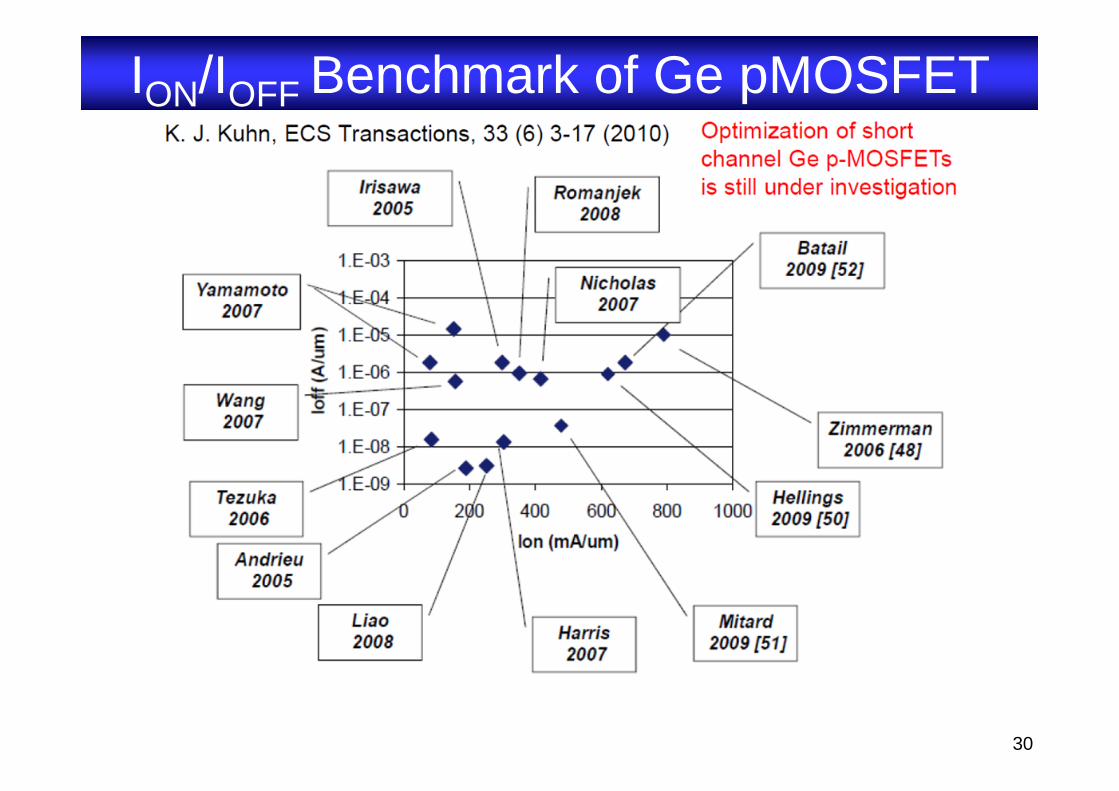
ION/IOFF Benchmark of Ge pMOSFET
30
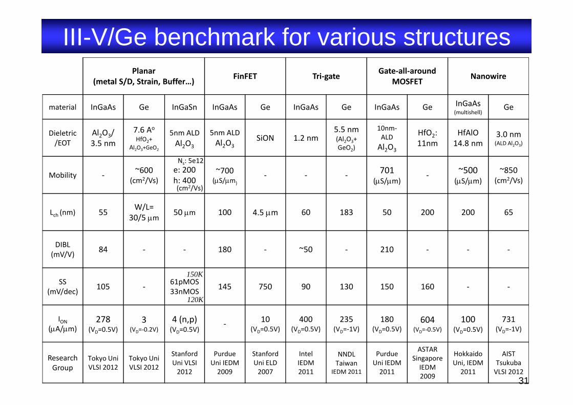
Planar(metal S/D, Strain, Buffer…)
FinFET Tri‐gateGate‐all‐around
MOSFETNanowire
material InGaAs Ge InGaSn InGaAs Ge InGaAs Ge InGaAs Ge InGaAs(multishell)
Ge
Dieletric/EOT
Al2O3/ 3.5 nm
7.6 Ao
HfO2+ Al2O3+GeO2
5nm ALDAl2O3
5nm ALD Al2O3
SiON 1.2 nm5.5 nm(Al2O3+GeO2)
10nm‐ALD Al2O3
HfO2:11nm
HfAlO14.8 nm
3.0 nm(ALD Al2O3)
Mobility ‐ ~600(cm2/Vs)
e: 200h: 400
~700(µS/µm)
‐ ‐ ‐ 701(µS/µm)
‐ ~500(µS/µm)
~850(cm2/Vs)
Lch (nm) 55W/L=
30/5 µm50 µm 100 4.5 µm 60 183 50 200 200 65
DIBL(mV/V)
84 ‐ ‐ 180 ‐ ~50 ‐ 210 ‐ ‐ ‐
SS(mV/dec)
105 ‐61pMOS33nMOS
145 750 90 130 150 160 ‐ ‐
ION(µA/µm)
278(VD=0.5V)
3(VD=‐0.2V)
4 (n,p)(VD=0.5V)
‐ 10(VD=0.5V)
400(VD=0.5V)
235(VD=‐1V)
180(VD=0.5V)
604(VD=‐0.5V)
100(VD=0.5V)
731(VD=‐1V)
ResearchGroup
Tokyo UniVLSI 2012
Tokyo UniVLSI 2012
Stanford Uni VLSI 2012
Purdue Uni IEDM 2009
Stanford Uni ELD 2007
IntelIEDM 2011
NNDL Taiwan
IEDM 2011
Purdue Uni IEDM 2011
ASTARSingapore IEDM 2009
Hokkaido Uni, IEDM
2011
AIST Tsukuba VLSI 2012
150K
120K
(cm2/Vs)
Ns: 5e12
III-V/Ge benchmark for various structures
31
More Moore approach
Advance Si-based CMOS devices and technologies
Technology benchmark
Challenges
Alternative channel material devicesTechnology benchmark
III-V, Ge-based devices
Emerging technologies(Tunnel FET, Junctionless FET, Carbon-based FET, MEMS,Spin-based Logic)
Conclusions
OutlineOutline
32

ION at LG = 50 µm pMOS: 4 µA/µmnMOS: 3.8 µA/µm
Achieving both N‐ and P‐type MOSFETon a single channel is possible
electron/hole mobility > 4000/900cm2/Vs was gained in a single channel material
In‐content of 20‐40% improves perfomance
Z. Yuan et al., pp.185, VLSI2012 (Stanford Uni)
InGaSb as channel material (stanford)
Electron MobilityHole Mobility
AlGaSb creates barrierfor both electrons and holes
SiSi
InGaSbInGaSb
33

Metal S/D and InAs buffer layer are usedas performance boosters.DIBL=84 mV/V and SS=105 mV/V was shown for Lch = 55 nm when In‐content washigher.
S. H. Kim et al., pp.177, VLSI2012 (Tokyo Uni)
Metal S/D InGaAs MOSFET (Tokyo Uni)
34

SS: nMOS: 90 (mV/decade)pMOS: 190 (mV/decade)
Si2H6 plasma passivation is employedwhich creates Si layer at interface.
Common gate stack (gate metal and dielectric) were used for both p‐ and n‐type
High intrinsic peak GM,Sat=of ~465 μS/μm at VDS=-1.1 V was achieved for LG=250 nm.
X. Gong, et al. (National Uni of Singapore), VLSI2012, p.99.
Common InGaAs‐GeSn gate stack (NUS)
LG= 5µmVGS-VTH= 0~2.0V
35

InGaAs nanowire transistor(Hokkaido Uni)InGaAs nanowire transistor(Hokkaido Uni)T. Fukui, et al. (Hokkaido Univ), IEDM2011, p.773.
Core-multishell InGaAs nanowires grown without buffer layer on Si substrate(bottom up approach)
At Vd = 1 V peak transconductance of 500 mS/mm is achieved (roughly x3 InGaAs nanowire)
36

TriTri--gate InGaAs QWgate InGaAs QW--FET(Intel)FET(Intel)M. Radosavljevic, et al.(Intel), IEDM2011, p.765.
Steepest SS and smallest DIBL ever reported (Wfin = 30nm)
Tri-gate structure has superiority electrostatic controllability compared to ultra-thin body planar structure
37

Gate all around InGaAs MOSFET(Purdue)Gate all around InGaAs MOSFET(Purdue)P. D. Ye, et al (Purdue Univ)., IEDM2011, p.769.
DIBL was suppressed down to
Lch = 50nm and
Gm,max =701mS/mm at Vds = 1V
Inversion mode In0.53Ga0.47As MOSFET with ALD Al2O3/WN with well electrostatic properties
Wfin= 50nm
Wfin= 30nm
38
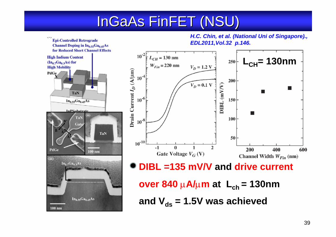
DIBL =135 mV/V and drive current
over 840 µA/µm at Lch = 130nm
and Vds = 1.5V was achieved
H.C. Chin, et al. (National Uni of Singapore)., EDL2011,Vol.32 p.146.
LCH= 130nm
InGaAs FinFET (NSU)InGaAs FinFET (NSU)
39

GeGe--nanowire pMOSFET (AIST,Tsukuba)nanowire pMOSFET (AIST,Tsukuba)
Using Ni-Ge alloy as metal S/D
Significantly reduces contact resistance
K. Ikeda, et al. (AIST, Tsukuba), VLSI2012, p.165.
High saturation current and high mobility
μeff = 855 cm2/Vs at Ns =5x1012cm-2
and saturation drain current of 731μA/μm at Vd = -1V
Lg= 65nm Wwire= 20nmVD= -1V
VD= -0.5V
VD=-0.05V
Vg-Vth= -2V
40

S-H. Hsu, et al. (NNDL,Taiwan), IEDM2011, p. 825.
Selective etching of high defect
Ge near Ge/Si interface is used which improves gate controllability.
ION/IOFF = 105 and SS= 130 mV/dec
And ION= 235 µm/µm at VD= -1V
Ge triangular pMOSFET (NNDL,Taiwan)Ge triangular pMOSFET (NNDL,Taiwan)
Ge Triangular
Ge Rectangular
Lg>2Wfin Lg<2Wfin
41

III-V (InGaAs, InAs,InGaSb,…)
Al2O3 Si-HfO2 Al2O3+HfO2 HfAlOx TaSiOx
ALD-Al2O3 is most commonly used as gate dielectric in planar or Multi-gateHfO2-only stacks have high Dit (combination of Al2O3 or Al or Si is used)
In0.53Ga0.47AsIn0.7Ga0.3As
Ge
Intel, IEDM 2010Hokkaido Uni, IEDM 2011NUS, VLSI 2012E. Kim, et al.,APL96, 012906
L. Chu, et al.,APL99, 042908
3.4 nm1.2 nm
Implementing highImplementing high--k material to IIIk material to III--V,GeV,Ge
By controlling the formation of GeOxat the interface, HfO2 and Al2O3show good results.
R. Zhang et al., VLSI2012,p16142

More Moore approach
Advance Si-based CMOS devices and technologies
Technology benchmark
Challenges
Alternative channel material devicesTechnology benchmark
III-V, Ge-based devices
Emerging technologies(Tunnel FET, Junctionless FET, Carbon-based FET, MEMS,Spin-based Logic)
Conclusions
OutlineOutline
43

Carbon‐based FET
Gate length (nm)10010Cu
t‐off frequ
ency ( GHz)
L. Liao, et al., Nature ,Vol.467 p.305.
F. Schwlerz, Nature Nano ,Vol.5 p.487.
GaAs mHEMT(20nm) SiMOSFET
(29nm)GaAs pHEMT(100nm)
100
1000
10
CNT
Graphene
J. P. Colinge et al., Nature Nano. 5(2010)225
A. D. Franklin et al., pp.525, IEDM2011 (IBM)
J. P. Colinge et al., Nature Nano. 5(2010)266
Junctionless Transistor
All‐spin logic device
1000
M. Lemme, Nanotech workshop ,2012
Input and output related via Spin-coherent channel
Emerging devices(future scaling trends)Emerging devices(future scaling trends)Carbon nanotube Graphene
44

A. Seabaugh, IEDM 2011 Short Course (University of Notre Dame)
Low IOFF, Low VDD, SS<60mV/decade
Tunnel FETTunnel FET
45
Band to band
tunneling
VDS=1V
SS=21mV/dec
VDS= 1V
HfAlOx
Gate
K. Tomioka et al., pp.47, VLSI2012 (Hokkaido University)

VDD 0.3~0.35VTFET 8x faster at the same power
“parameter variation is not a significant factor for differentiation
between MOSFET and TFET”
A. Seabaugh, IEDM 2011 Short Course (University of Notre Dame)
TFET vs. MOSFET at low VTFET vs. MOSFET at low VDDDD
46

A. Villalon, pp.49, VLSI 2012 (CEA-LETI)
190mV/dec
Tunnel FET (Si)Tunnel FET (Si)
X in Si1-xGex is optimized to allow for efficient BTBT
Gate Voltage (V)
Reducing SiGe Body thickness improvesSubthreshold swing.
LG= 200nm
130mV/dec
ION/IOFF~105
47

VDS=1V
K. Tomioka et al., pp.47, VLSI2012 (Hokkaido University)
SS=110mV/decSS=21mV/dec
VDS= 1V
HfAlOx
Gate
NW Diameter= 30nmSS of TFET is function of VG due to Zener tunnel current
Tunnel FET (IIITunnel FET (III--V)V)
Conventional FET limitSS= 60 mV/dec
Minimum SS= 21 mV/dec is reached due to optimized series resistance of contact, undoped InAs and InAs/SiION/IOFF~106 at VDS= 1.0V (ION= 1Aµ/µm)
48

K. Tomioka et al., pp.47, VLSI2012 (Hokkaido University)
A. Seabaugh, IEDM 2011 Short Course (University of Notre Dame)
Device structureDevice structure
49

A. Seabaugh, IEDM 2011 Short Course (University of Notre Dame)
measured III-V channel TFETs
Tunnel FET performance comparisonTunnel FET performance comparison
Is the average swing when VTH=VDD/2VOFF=0
Most common SS which is the inverse of ID-VGS slopeat the steepest part
SMIN:
SEFF:
VGS
I D
Ith
IOFF
VTHVoff
Average SS:
VTH=VDD/2
Effective SS:
VOFF=0
50
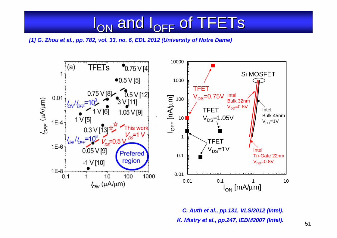
[1] G. Zhou et al., pp. 782, vol. 33, no. 6, EDL 2012 (University of Notre Dame)
IIONON and Iand IOFFOFF of TFETsof TFETs
C. Auth et al., pp.131, VLSI2012 (Intel).K. Mistry et al., pp.247, IEDM2007 (Intel).
0.01
0.1
1
10
100
1000
10000
0.01 0.1 1 10ION [mA/µm]
I OFF
[nA
/µm
]
TFET VDS=1V
Si MOSFET
IntelBulk 32nmVDD=0.8V
IntelTri-Gate 22nmVDD=0.8V
Intel Bulk 45nmVDD=1V
TFET VDS=0.75V
TFET VDS=1.05V
51
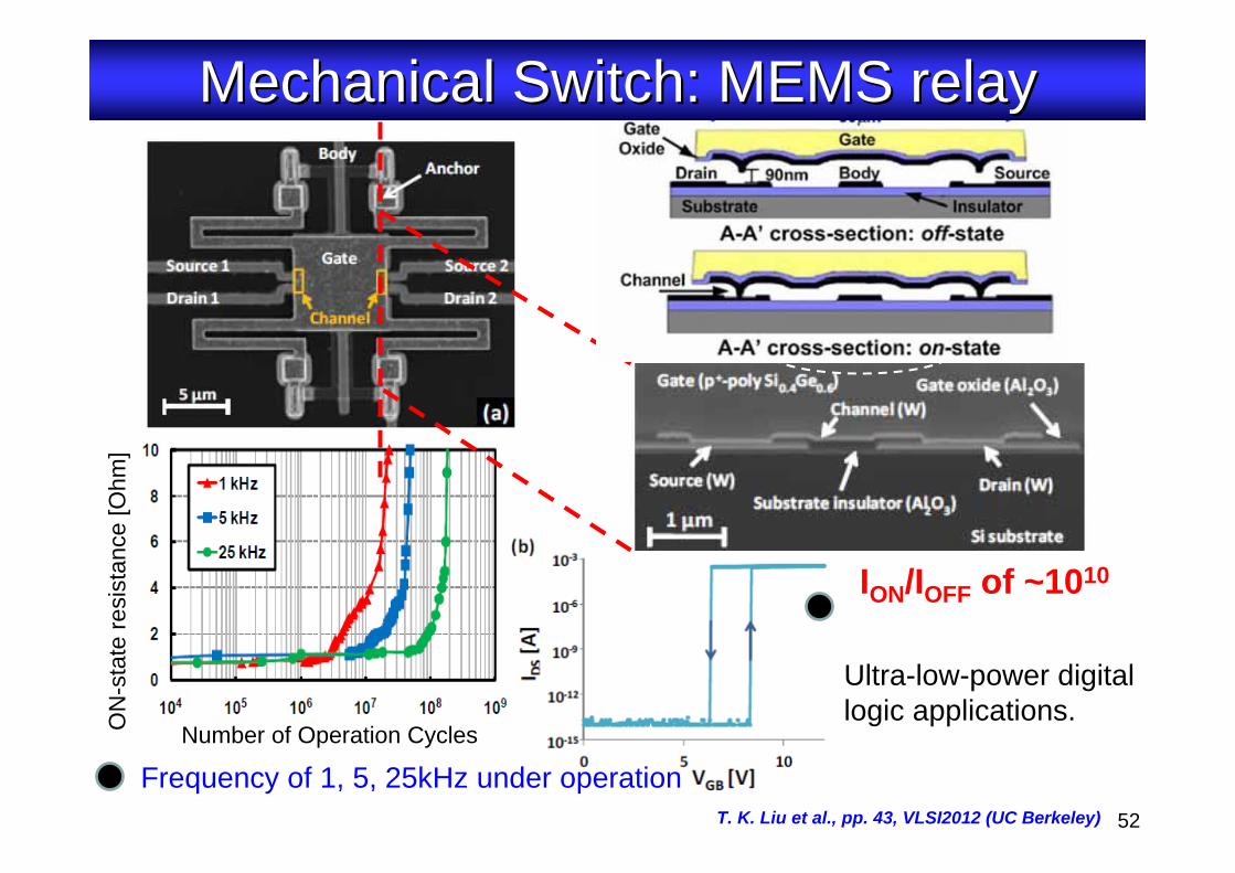
ION/IOFF of ~1010
T. K. Liu et al., pp. 43, VLSI2012 (UC Berkeley)
ON
-sta
te re
sist
ance
[Ohm
]
Number of Operation Cycles
Ultra-low-power digital logic applications.
Frequency of 1, 5, 25kHz under operation
Mechanical Switch: MEMS relayMechanical Switch: MEMS relay
52

Silicon nanowire is uniformly doped
J. P. Colinge et al., Nature Nano. 5(2010)225
Gate material is oppositepolarity polysilicon
Lg= 1µm
10nm
30.5nm
Lg= 1µmWwire= 30nm
Nanowire Junctionless TransistorNanowire Junctionless Transistor
53
n+ n+n n+ n+pS DS D
pn junctionno junction
Junctionless Conventional

IM : Conventional Inversion ModeJAM LD : Janctionless Accumulation Mode with low dopeJAM HD : Janctionless Accumulation Mode with high dope
JAM devices have reduced gate control and degraded short-channel characteristics relative to IM
Si Junctionless Transistor (Intel)Si Junctionless Transistor (Intel)R. Rios et al., EDL. 32(2011)1170 (Intel)
403020 403020 403020Lg (nm) Lg (nm) Lg (nm)
Not suitable for high-performance logic (high Ion and moderate Ioff)54

K. Banerjee, UC Santa Barbara, G-COE PICE International Symposium on Silicon Nano Devices in 2030
Carbon nanotube and GrapheneCarbon nanotube and Graphene
SWCNT : single wall carbon nanotubeGNR : graphene nano ribbon
Carbon materials for FET applications ・ an ultra-thin body for aggressive channel length scaling・ excellent intrinsic transport properties
55

A. D. Franklin et al., pp.525, IEDM2011 (IBM)
SubSub--10nm carbon nanotube transistor10nm carbon nanotube transistor
Transistor operation with Lch of 9nm56

Z. Chen et al., pp.509, IEDM2008 (IBM)
Graphene FieldGraphene Field--effect Transistoreffect TransistorJ. B. Oostinga et al., Nature Materials 7 (2008) 151
・Ambipolar Characteristics
・Bi-layer graphene and double gates can open the gap
57・ Ioff is very large No bandgap

T. Marukame et al., pp.215, IEDM2009 (Toshiba)
Magnetic tunnel junction on S/D
Read/write are enabled by using ferromagnetic electrodes and Spin-polarized current
Lg = 1µm
Spin transfer Torque Switching MOSFETSpin transfer Torque Switching MOSFET
58

Summary of Emerging Technology pro/consSummary of Emerging Technology pro/cons
59
Advantage Issues
TFETLower Vdd
Lower IOFF Lower ION
CNT FET Higher transport velocityLow density and
alignment, reproducibility, integration
Graphene FET RF application Huge IOFF
MEMS Extremely low leakage Ultra-low digital logic
EnduranceSlow speed, scalability
Junctionless FET CMOS process compatibility
Worse gate control in short-channel
Spin FETLow power, suitable for
memory (nonvolatile info storage)
Low efficiency of spin injection

More Moore approach
Advance Si-based CMOS devices and technologies
Technology benchmark
Challenges
Alternative channel material devicesTechnology benchmark
III-V, Ge-based devices
Emerging technologies(Tunnel FET, Junctionless FET, Carbon-based FET, MEMS,Spin-based Logic)
Conclusions
OutlineOutline
60

Conclusions for logicConclusions for logic
Alternative channel device needs more time to catch up Si.
Si based CMOS is still the mainstream for downsizing until sub-10 nm.
Emerging device technologies are still in research level.
61
New structure (fin, try, nanowire-gate, or ET-SOI). New materials for high-k gate, and metal S/D.
Fin, try, nanowire-gate structures become popular. High-k gate needs to be improved.
AcknowledgementAcknowledgement
I would like to express appreciation to Dr. Takamasa Kawanago and Mr. Darius Zade
of Tokyo Institute of Technologyfor the material preparation.
62

Appendix
63

C. Auth et al., pp.131, VLSI2012 (Intel)
・Steep SS
・low DIBL
・Improved Ion (strain, HK/MG)
1-55-2020-100IOFF (nA/um)
343430LGATE (nm)
0.90.90.9TOX,E (nm)
SPMPHP
1-55-2020-100IOFF (nA/um)
343430LGATE (nm)
0.90.90.9TOX,E (nm)
SPMPHP
FinFET(TriFinFET(Tri--Gate Transistors)Gate Transistors)
64