Scalable RF Receivers for Large Antenna Arrays
66
Scalable RF Receivers for Large Antenna Arrays Konstantin Trotskovsky Elad Alon, Ed. Ali Niknejad, Ed. Ilan Adler, Ed. Electrical Engineering and Computer Sciences University of California at Berkeley Technical Report No. UCB/EECS-2020-188 http://www2.eecs.berkeley.edu/Pubs/TechRpts/2020/EECS-2020-188.html December 1, 2020
Transcript of Scalable RF Receivers for Large Antenna Arrays
Scalable RF Receivers for Large Antenna Arrays
Konstantin TrotskovskyElad Alon, Ed.Ali Niknejad, Ed.Ilan Adler, Ed.
Electrical Engineering and Computer SciencesUniversity of California at Berkeley
Technical Report No. UCB/EECS-2020-188http://www2.eecs.berkeley.edu/Pubs/TechRpts/2020/EECS-2020-188.html
December 1, 2020

Copyright © 2020, by the author(s).All rights reserved.
Permission to make digital or hard copies of all or part of this work forpersonal or classroom use is granted without fee provided that copies arenot made or distributed for profit or commercial advantage and that copiesbear this notice and the full citation on the first page. To copy otherwise, torepublish, to post on servers or to redistribute to lists, requires prior specificpermission.
Scalable RF Receivers for Large Antenna Arrays
by
Konstantin Trotskovsky
A dissertation submitted in partial satisfactionof the requirements for the degree of
Doctor of Philosophy
in
Engineering - Electrical Engineering and Computer Sciences
in the
Graduate Division
of the
University of California, Berkeley
Committee in charge:
Professor Elad Alon, ChairProfessor Ali M. Niknejad
Professor Ilan Adler
Fall 2018

Scalable RF Receivers for Large Antenna Arrays
Copyright c© 2018
by
Konstantin Trotskovsky

Abstract
Scalable RF Receivers for Large Antenna Arrays
by
Konstantin Trotskovsky
Doctor of Philosophy in Engineering - Electrical Engineering and Computer Sciences
University of California, Berkeley
Professor Elad Alon, Chair
The ongoing exponential mobile traffic increase is continuing to push the requirements of wire-less communication systems. Currently in dense urban areas the major limitation to the capacityof wireless links is interference between different users. Massive MIMO is a promising technologyto address this challenge, where directional spatial beams are formed by an antenna array on abase station, each serving a different user. This concept is currently verified using commercialgeneral-purpose analog hardware, with power consumption in the kW range for large arrays.
This thesis focuses on energy-efficient RF receiver design for Massive MIMO systems. In orderto be energy-efficient, the system requirements for a large antenna array receiver are different from aconventional single-antenna receiver. We use the fact that the noise of each receiver is uncorrelatedacross the array, so we can save power by using receivers with larger noise, while still meetingthe link budget requirements. However, receiver linearity cannot be relaxed due to the digitalbeamforming used in the system.
To address these challenges a novel RF receiver architecture is proposed, using a mixer-firstapproach with mixer switch resistance larger than 50Ω. Configurable mixer and baseband Gm sizesallow the receiver to trade noise figure for power consumption and use the same receiver for variousarray sizes and array-level noise specifications. Harmonic recombination is performed early in thesignal path, enabling rejection of harmonic blockers up to -10dBm of power.
This architecture was implemented in a first chip prototype. Scalable element noise figureresults in sub-2.5 dB array-level noise figure with 16 to 64 antennas and <368 mW total powerconsumption, for a frequency range of 0.25-1.7GHz.
In the second chip we perform an optimized design using the Berkeley Analog Generator (BAG).The proposed generator design methodology produces instances with optimum power consumptionfor a given noise figure specification. An instance of this generator is implemented in the chip,showing power consumption improvement of 50% and wider frequency range of 1-6GHz comparedto the first chip.
1

Contents
i

List of Figures
ii

List of Tables
iii
Acknowledgements
I am very grateful to many people in Berkeley that helped me through my PhD here. FirstI would like to thank my advisors, professors Elad Alon and Ali Niknejad. I feel very fortunateto work with them. The weekly meetings with Elad were something that I was expecting for theentire week. I was always impressed by Elad’s ability to switch to a new solution and throw awaythe old one, no matter how much did we invest in it in the past. His levels of energy and optimismare something to aspire for me. I am very grateful to Ali for his offer to be co-advised by him.Ali provided a new insight and a different perspective to the problems that I was facing. I alsohad a great time GSI-ing 242A and 105 with him. Teaching was a hard experience for me in thebeginning, and Ali was very helpful and supportive.
I would also like to thank professor Bora Nikolic for taking part in my quals committee andhelping out during the project meetings that we had over the years. Thanks to professor PaulWright for serving in my quals committee and providing feedback. Special thanks to professor IlanAdler for being a member in my dissertation committee, even though I asked him so late.
The students in BWRC make this place very special. I feel that a large part of what I learnedin the past 5 years was from interacting with them. In the first eWallpaper project we started asa team of inexperienced students, and this chip would not be possible to build without the effortof all of them. I feel lucky to work with Amy Whitcombe on this project and especially duringthe measurements and paper writing stage. I thought that I am a hard-working person that paysattention to details, but working with Amy had set a new bar for me. Her work ethics, willingnessto help and positive attitude made our work a great experience. During the chip and board designI was fortunate to work with Pengpeng Lu. Pengpeng’s patience and sense of humor made manyhours that we spent together both funny and productive. Many thanks to Greg LaCaille who helpedme with various circuit problems and had so many great ideas. Antonio Puglielli was a brilliantguy who made every problem look easy. Greg’s and Antonio’s help with top-level integration madethis tapeout possible. Thanks to Nathan Narevsky, Eric Chang and Zhongkai Wang for their helpand advice. Thanks to Greg Wright from Nokia who was very enthusiastic about the project andprovided many helpful inputs.
In my second project I had to learn how to use BAG, and I would like to thank Eric Changfor being patient and helpful answering all my questions. In the early stages I had many questionsand Eric was always patient and quick to respond. I am very happy that I got to know MarkoKosunen and worked with him on the chip flow and integration. His continuous efforts to makethe chip work and meet the deadline made this chip possible. I learned a lot from Marko, bothon the technical side and on the problem solving methodology. Thanks to Nathan, Zhongkai andPengpeng for their help with the chip design.
I was lucky to be involved in two research groups of my two advisors and get to know manysmart people. Thanks to Seobin Jung, Yida Duan, Jaeduk Han, Bonjern Yang, Nick Sutardja,Emily Naviasky, Ali Moin, Steven Callender, Andrew Townley, Nai-Chung Kuo, Lorenzo Iotti,Nima Baniasadi, Bo Zhao, Sashank Krishnamurthy, Yi-An Li, Luya Zhang, Ali Ameri and MatthewAnderson. Outside of my research groups, I would like to thank Luke Calderin, Sameet Ramakr-ishnan, Stevo Bailey, Mirjana Videnovic-Misic, Rachel Hochman, Amanda Pratt, Nandish Mehta,Sharon Xiao, Sidney Buchbinder, Filip Maksimovic, Krishna Settaluri and John Wright.
The staff members make BWRC a great place to work. Special thanks to Candy Corpus whowas extremely friendly and helpful in solving any administrative problem. Candy’s optimism andhard work make BWRC a great place to be in. Thanks a lot to Brian Richards who was very
iv
helpful and optimistic during the hard tapeout times. James Dunn was very quick to respond toany problem, and made sure that it is resolved no matter how busy he was. Fred Burghardt madethe lab a great place to work and was always happy to help. Many thanks to Anita Flynn forher help with PCB design. Thanks to Ajith Amerasekera, Melissa Trevizo, Amber Sanchez, OliviaNolan and Sarah Jordan for their help.
I would like to thank my family, my mother Elena and sister Maya. Being far away for a longtime was a challenge for all of us, and I am very grateful to them for their support during all theseyears. My last and great thanks is to my fiancee Anna, who made my life far better since we met.I am looking forward to our future life together.
v

Chapter 1
Introduction
We are living in a time of exponential mobile traffic increase. In the past 5 years the yearlymobile traffic increased by 55-70% per year [? ]. This trend is expected to continue at least in thenext 5 years, projected in Figure ??. The total mobile traffic is expected to grow by a factor of 5in this period.
Figure 1.1. Global mobile data traffic (exabytes per month). Exponential global trafficincrease over time is projected.
There are two contributors to the total mobile traffic increase. First, the number of mobiledevices is growing. Second, and more importantly, the mobile traffic per device is growing as well.The projection is that from 2017 to 2023 the number of worldwide smartphones will increase by
1

8% per year, while the mobile traffic per smartphone will increase by 31% per year [? ]. This trendhappens all over the world, as illustrated in Figure ??.
Figure 1.2. Mobile data traffic per active smartphone (gigabytes per month). Data trafficincrease per user is exponential all over the world.
To addess this increase in mobile traffic, the 3rd Generation Partnership Project (3GPP) createdthe specifications for Long-Term Evolution (LTE) in mobile communication. Approximately everyyear a new release is made enabling higher data rates and denser deployments. We now see atransition from a 4G LTE standard to 5G, when the current Release 15 is the first to have 5Gspecifications [? ]. However, as shown in Figure ??, the transition between 4G and 5G will takemany years, and in 2023 only about 20% of the data traffic will be through the 5G standard.
In the past decades many different techniques were used to address the exploding demandfor data traffic. Two main challenges should be addressed: increasing the data rate per user,and supporting larger number of users simultaneously. We will briefly discuss them and see thatcontinuing to improve them is becoming more and more difficult.
Ingoring other users, the main techniques to improve the data rate per user are increasedbandwidth, improved channel coding and using higher constellations.
• Bandwidth is the most straightforward way to increase the possible data rate. However thefrequency allocation in RF frequencies is very dense and extremely expensive in RF frequen-cies. One possible direction that is under consideration for 5G is starting to use mm-wavefrequencies where more bandwidth is available. This creates new challenges that we willdiscuss later.
• Channel coding can enable the usage of smaller SNR for the same received data rate. Mod-ern coding schemes are already very close to Shannon’s limit, leaving very little room forimprovement in the required SNR.
• Higher constellation enables larger channel capacity for the same bandwidth. However sincethe channel capacity is logarithmic with the SNR, there are diminishing returns in the chan-
2

nel capacity when improving SNR (Figure ??). In addition, the hardware implementationbecomes extremely challenging for higher constellations.
Figure 1.3. Shannon’s limit SNR = 2C/B − 1 makes it impractical to address exponentialchannel capacity growth by more complex constellation. For example, 3dB (2x) capacityfrom 8bps/Hz to 16bps/Hz requires 24dB (250x) higher SNR.
In less dense rural areas these are the main challenges. However, in dense urban areas largenumbers of users need to be served simultaneosly. Here two main questions arise: how to sharethe wireless channel between different users, and how to prevent inter-user interference. Severaltechniques have been used to address these issues: Frequency-Division Multiple Access or FDMA(allocating different frequencies to different users), Time-Division Multiple Access or TDMA (al-locating different time slots to different users), and Code-Division Multiple Access or CDMA (al-locating different coding schemes to different users). The main limitation of these techniques isthat they share the entire network capacity between the users, so adding more users will result inreduced user capacity.
To address these issues, spatial multiplexing is a promising direction. Multiple input-multiple-output (MIMO) technology is already using multiple antennas on both receive and transmit sides,taking advantage of several multi-path propagations. Multi-user MIMO (MU-MIMO) offers evenhigher capacities due to simultaneous communication to different users.
This approach is part of the Berkeley Wireless Research Center (BWRC) vision of a universalnext-generation (xG) network [? ], summarized in Figure ??. A large antenna array access point(xG Hub) provides connectivity to many devices using highly directional beams. The large array cansupport various communication standards, devices and ranges. Beamforming implements spatialselectivity and enables spectrum re-use and simultaneous communication to many users.
This vision has a lot in common with the recently popular Massive MIMO concept. The keyidea of Massive MIMO is the use of a large number of base station antennas and much smallernumber of users. Therefore, using beamforming, the large array can form a beam to every user,greatly improving the interference between the users and re-using the spectrum.
Several massive MIMO systems have been recently demonstrated in academia and industry.
3

Figure 1.4. Berkeley Wireless Research Center (BWRC) xG (x ≥ 5) vision for next gener-ation wireless standard.
Their main goal was to explore the system performace rather than to implement an efficient hard-ware. For the RF transceivers off-the-shelf components were used. The Ngara system [? ] operatedat 806MHz for the uplink and 638MHz for the downlink and used discrete components. The Argos[? ] and ArgosV2 [? ] systems operated at the 2.4GHz ISM band and used Maxim 2829 WiFitransceiver, while ArgosV3 [? ] used a wideband Lime Microsystems LMS7002M transceiver op-erating at 50MHz-3.8GHz. Lund University [? ], National Instruments [? ] and Samsung [? ]have demonstrated systems using NI USRP RIO Software-Defined-Radio transceivers, operating at3.7GHz, 50MHz-6GHz and 3.4-3.6GHz respectively.
These systems have 32-160 antennas and serve 10-16 users. The off-the-shelf RF transceiversused consume 100s of mW, making the array RF power consumption lie in the kW range. Thispower consumption is already huge, and will be even larger if more antennas are used to serve moreusers.
So far no custom-design RF IC receivers were demonstrated in Massive MIMO systems. Thegoal of this work is to implement an integrated energy-efficient RF receiver tailored for MassiveMIMO applications. In Chapter ?? we discuss the RF receiver design considerations with an empha-sis on the differences between a receiver for large antenna array and a more common single-antennareceiver. In Chapter ?? we describe the circuit architecture to address the array requirementsand show a first version implementation of a chip for Massive MIMO applications. Chapter ??describes the second chip implementation, fully designed using Berkeley Analog Generator (BAG)and optimized for energy-efficiency performance. Finally, Chapter ?? summarizes the thesis.
4
Chapter 2
System Design Considerations
In this chapter we will discuss the RF receiver design considerations for a large antenna array.Designing an RF receiver for a single-antenna system is a well-known procedure, but the fact thatthe receiver is intended to be used in a large array changes the specifications for the receiver. Inother words, we will show what can we change in the RF receiver design in order to achieve theoverall array performance in an energy-efficient manner.
The design considerations details of the entire Massive MIMO system can be found in [? ] and[? ]. Here we will focus on the implications on the RF receiver part of the system. A detaileddescription of the ADC design considerations is presented in [? ].
2.1 Noise and energy-efficiency
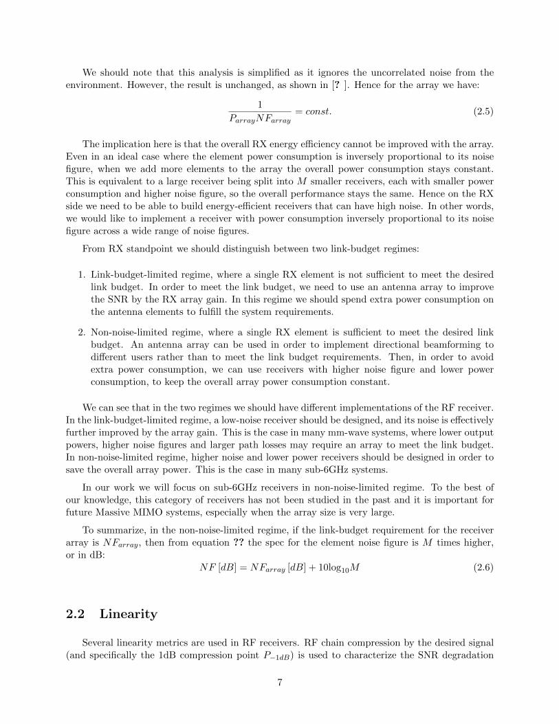
To understand the impact of the receiver noise performance on the overall array energy effi-ciency, we will compare the transmitter (TX) and the receiver (RX) behavior in large arrays. Thisis summarized in Figure ??.
We will assume that we have an array of M antennas, each has an output power of Pout forthe TX side and a noise figure of NF for the RX side. Then both for TX and RX the total arraypower consumption is proportional to M :
Parray ∝M (2.1)
On the TX side with beamforming the main beam points to the user direction, and we havespatial summation of the electromagnetic waves. So the electric fields are summed in the air, whichis equivalent to voltage summation of the transmitter outputs. Thus when we have M transmitterswith output power of Pout, the array equivalent isotropic radiated power (EIRP) is proportional toM2Pout:
EIRParray ∝M2Pout (2.2)
It means that the ratio of the EIRP to the array power consumption is proportional to the
5

Pout
Pout
Pout
M
M
Array power
consumption
Array
EIRP
(dB)
TX
NF
NF
NF
M
M
Array power
consumption
Array
NF
(dB)
RX
Figure 2.1. The impact of the array elements on the overall TX and RX array performance.
array size:EIRParray
Parray∝M (2.3)
The implication is that the overall TX energy efficiency can be improved when using the array.If we need a certain array EIRP to fulfill our link budget, we can reduce the overall array TXpower consumption by using more array elements, each having lower output power. The arraypower consumption cannot be reduced indefinitely due to overhead power that does not scale withthe array size, resulting in optimum array size for given array EIRP, transmitter efficiency andoverhead power [? ]. Generally speaking, for a large array we need efficient low output powertransmitters with low overhead power.
However, on the RX side the analysis is different. The noise added by each receiver in the arrayis uncorrelated across the antenna elements. Thus while the output signal power is proportional toM2 (same as in the TX case), the output noise power is proportional to M . This is illustrated inFigure ?? for M = 4 elements.
Figure 2.2. Illustration of uncorrlated noise averaging for M = 4 array elements.
Consequently the array SNR is proportional to M , or equivalently:
NFarray =NF
M(2.4)
6
We should note that this analysis is simplified as it ignores the uncorrelated noise from theenvironment. However, the result is unchanged, as shown in [? ]. Hence for the array we have:
1
ParrayNFarray= const. (2.5)
The implication here is that the overall RX energy efficiency cannot be improved with the array.Even in an ideal case where the element power consumption is inversely proportional to its noisefigure, when we add more elements to the array the overall power consumption stays constant.This is equivalent to a large receiver being split into M smaller receivers, each with smaller powerconsumption and higher noise figure, so the overall performance stays the same. Hence on the RXside we need to be able to build energy-efficient receivers that can have high noise. In other words,we would like to implement a receiver with power consumption inversely proportional to its noisefigure across a wide range of noise figures.
From RX standpoint we should distinguish between two link-budget regimes:
1. Link-budget-limited regime, where a single RX element is not sufficient to meet the desiredlink budget. In order to meet the link budget, we need to use an antenna array to improvethe SNR by the RX array gain. In this regime we should spend extra power consumption onthe antenna elements to fulfill the system requirements.
2. Non-noise-limited regime, where a single RX element is sufficient to meet the desired linkbudget. An antenna array can be used in order to implement directional beamforming todifferent users rather than to meet the link budget requirements. Then, in order to avoidextra power consumption, we can use receivers with higher noise figure and lower powerconsumption, to keep the overall array power consumption constant.
We can see that in the two regimes we should have different implementations of the RF receiver.In the link-budget-limited regime, a low-noise receiver should be designed, and its noise is effectivelyfurther improved by the array gain. This is the case in many mm-wave systems, where lower outputpowers, higher noise figures and larger path losses may require an array to meet the link budget.In non-noise-limited regime, higher noise and lower power receivers should be designed in order tosave the overall array power. This is the case in many sub-6GHz systems.
In our work we will focus on sub-6GHz receivers in non-noise-limited regime. To the best ofour knowledge, this category of receivers has not been studied in the past and it is important forfuture Massive MIMO systems, especially when the array size is very large.
To summarize, in the non-noise-limited regime, if the link-budget requirement for the receiverarray is NFarray, then from equation ?? the spec for the element noise figure is M times higher,or in dB:
NF [dB] = NFarray [dB] + 10log10M (2.6)
2.2 Linearity
Several linearity metrics are used in RF receivers. RF chain compression by the desired signal(and specifically the 1dB compression point P−1dB) is used to characterize the SNR degradation
7
when the desired signals at the input of the receiver become large. The weak-nonlinearity inter-modulations (and specifically second and third order intercept points IP2 and IP3) characterize theimpact of nearby blockers with moderate input powers on the SNR of the desired signal. Finally,large nearby blockers cause the receiver gain of the desired signal to compress and the thermalnoise floor to increase, both degrading the desired SNR.
When analyzing the impact of the array on the overall linearity performance, we observe thatthe inband linearity (the path of the signal) is unaffected by the fact that we are using an array.This is due to the fact that nonlinearity is a systematic feature of the array elements, so to firstorder each element has the same nonlinear characteristics. However, the blocker impact is verydifferent. The main idea of Massive MIMO systems is to cancel the blockers and create directionalbeams that will enable larger signal-to-interferer ratios. Hence from the analog design standpoint,an important question is how exactly the blockers can be cancelled.
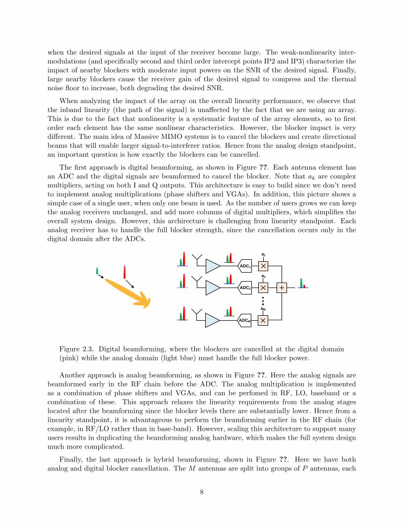
The first approach is digital beamforming, as shown in Figure ??. Each antenna element hasan ADC and the digital signals are beamformed to cancel the blocker. Note that ak are complexmultipliers, acting on both I and Q outputs. This architecture is easy to build since we don’t needto implement analog multiplications (phase shifters and VGAs). In addition, this picture shows asimple case of a single user, when only one beam is used. As the number of users grows we can keepthe analog receivers unchanged, and add more columns of digital multipliers, which simplifies theoverall system design. However, this archirecture is challenging from linearity standpoint. Eachanalog receiver has to handle the full blocker strength, since the cancellation occurs only in thedigital domain after the ADCs.
ADC1
a1
a2
aM
ADC2
ADCM
Figure 2.3. Digital beamforming, where the blockers are cancelled at the digital domain(pink) while the analog domain (light blue) must handle the full blocker power.
Another approach is analog beamforming, as shown in Figure ??. Here the analog signals arebeamformed early in the RF chain before the ADC. The analog multiplication is implementedas a combination of phase shifters and VGAs, and can be perfomed in RF, LO, baseband or acombination of these. This approach relaxes the linearity requirements from the analog stageslocated after the beamforming since the blocker levels there are substantially lower. Hence from alinearity standpoint, it is advantageous to perform the beamforming earlier in the RF chain (forexample, in RF/LO rather than in base-band). However, scaling this architecture to support manyusers results in duplicating the beamforming analog hardware, which makes the full system designmuch more complicated.
Finally, the last approach is hybrid beamforming, shown in Figure ??. Here we have bothanalog and digital blocker cancellation. The M antennas are split into groups of P antennas, each
8

a1
ADC
a2
aM
Figure 2.4. Analog beamforming, where the blockers are cancelled at the analog domain(light blue) while the digital domain operates with reduced blocker levels.
group performing analog beamforming with a single ADC. The P digital signals are then digitallybeamformed to create the final beam. The idea here is that each group formes a partial beam thatcancels some portion of the blockers, relaxing the linearity requirements from the following analogstages.
b1
b2
bN
a1,1
ADC
a1,2
a1,P
Figure 2.5. Hybrid beamforming, where the blockers are cancelled in part in the analogdomain (light blue) and in part in the digital (pink) domain.
The choice of the different beamforming architectures depends mainly on the speed of thedigital data and its power consumption. In RF frequencies the channel bandwidth is relatively low(usually tens of MHz), so we can build a digital beamforming system with moderate digital powerconsumption. However in mm-wave systems the channel bandwidths are several GHz and the digitalpower consumption becomes very large, so some amount of analog beamforming is necessary. Hencemm-wave massive MIMO systems are typically using hybrid beamforming. Analog beamformingis too complicated for multi-user MIMO systems, and is mainly used in traditional phased arrayapplications where a single beam is formed.
In our system we operate in the sub-6GHz frequency range with channel bandwidths of tens ofMHz. Hence the digital power consumption is moderate, and we can use digital beamforming tosimplify the overall system and enable easier support of many users. However, the implication isthat the analog receiver part has to be very linear to support large blockers before being digitizedby the ADCs.
9

2.3 Chip specifications
After a general discussion about the noise and linearity implications on a receiver design in alarge array system, we will summarize the specifications for our first receiver prototype. We are nottargeting any specific application, like WiFi or LTE, but rather want to build a system that can beused for various applications, as shown in the xG vision in Figure ??. Hence we can briefly look atthe current communication standards like WiFi and LTE, and try to derive the initial specificationsfor our system.
2.3.1 Frequency range and bandwidth
The cellular LTE standard supports 1.4, 5, 10, 15, and 20 MHz channel bandwidths [? ]. Italso supports carrier aggregation, in which up to 5 bands can be used simultaneously to enhancebandwidth. Smaller bandwidths are supported for legacy compatibility with existing standardslike GSM and CDMA. while larger bandwidths are used to support higher data rates for modernwireless systems. LTE operates over many of frequency bands, from 700MHz up to 3.8GHz.
The wireless local area network (WLAN) protocol or Wi-Fi is the most common protocolproviding wireless internet access to laptops and smartphones. Since its introduction in 1997 as theIEEE 802.11 standard, many updates to the standard have been implemented to support higherdata rates and more frequency bands to address the increasing demand. WiFi operates in industrial,scientific and medical (ISM) and Unlicensed National Information Infrastructure (U-NII) bands.Today most WiFi devices are operating in the 2.4GHz band of 2.412-2.484GHz (802.11b, 802.11g,and 802.11n) and the 5GHz band of 5.15-5.875GHz (802.11a, 802.11n, and 802.11ac) [? ]. Inaddition, 802.11ad is using 60GHz bands. All 2.4GHz and 5GHz standards support 20MHz channelbandwiths, while 802.11n and 802.11ac also support 40MHz channels. The 802.11ac standard canalso support 80 and 160 MHz bandwidths.
For our chip we will support a broad 700MHz to 6GHz range to cover all possible LTE and WiFibands, as well as other possible bands in between. In terms of channel bandwidth we will use 20MHzchannels (10MHz base-band bandwidth) for our chip. Supporting several channel bandwidths ispossible, and was demonstrated in [? ], [? ] and [? ], but the overhead required to do so is largeand not required to illustrate our research goals.
2.3.2 Blocker tolerance
As we have seen in section ??, when we use digital beamforming, the RF receiver needs to beable to handle large blocker powers, since the blockers are only cancelled after the conversion bythe ADCs. LTE standards have specifications of the adjacent channel interferers and out-of-bandinterferers resilience. An example of the power levels that an LTE receiver should tolerate is shownin Figure ??. This example has relatively relaxed blocker specs, only blockers further than 85MHzfrom the signal can be as high as -15dBm.
However, WiFi operates in unlicensed band and has to co-exist with other devices that use theISM band, like Bluetooth devices, cordless phones and microwave ovens. The received power in theWiFi band can be estimated by the free-space path loss (FSPL) in the Friis transmission equation:
10
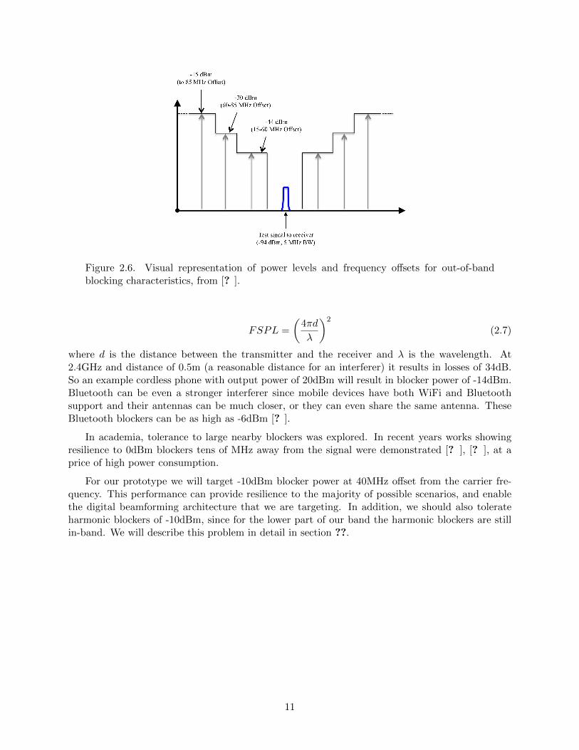
Figure 2.6. Visual representation of power levels and frequency offsets for out-of-bandblocking characteristics, from [? ].
FSPL =
(4πd
λ
)2
(2.7)
where d is the distance between the transmitter and the receiver and λ is the wavelength. At2.4GHz and distance of 0.5m (a reasonable distance for an interferer) it results in losses of 34dB.So an example cordless phone with output power of 20dBm will result in blocker power of -14dBm.Bluetooth can be even a stronger interferer since mobile devices have both WiFi and Bluetoothsupport and their antennas can be much closer, or they can even share the same antenna. TheseBluetooth blockers can be as high as -6dBm [? ].
In academia, tolerance to large nearby blockers was explored. In recent years works showingresilience to 0dBm blockers tens of MHz away from the signal were demonstrated [? ], [? ], at aprice of high power consumption.
For our prototype we will target -10dBm blocker power at 40MHz offset from the carrier fre-quency. This performance can provide resilience to the majority of possible scenarios, and enablethe digital beamforming architecture that we are targeting. In addition, we should also tolerateharmonic blockers of -10dBm, since for the lower part of our band the harmonic blockers are stillin-band. We will describe this problem in detail in section ??.
11
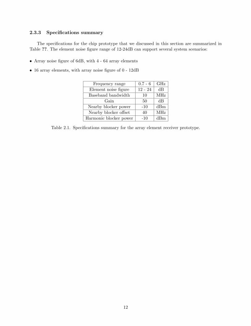
2.3.3 Specifications summary
The specifications for the chip prototype that we discussed in this section are summarized inTable ??. The element noise figure range of 12-24dB can support several system scenarios:
• Array noise figure of 6dB, with 4 - 64 array elements
• 16 array elements, with array noise figure of 0 - 12dB
Frequency range 0.7 - 6 GHz
Element noise figure 12 - 24 dB
Baseband bandwidth 10 MHz
Gain 50 dB
Nearby blocker power -10 dBm
Nearby blocker offset 40 MHz
Harmonic blocker power -10 dBm
Table 2.1. Specifications summary for the array element receiver prototype.
12
Chapter 3
A 0.25-1.7GHz, 3.9-13.7mW
Power-Scalable, -10dBm Harmonic
Blocker-Tolerant Mixer-First
RF-to-Digital Receiver
3.1 Chip architecture
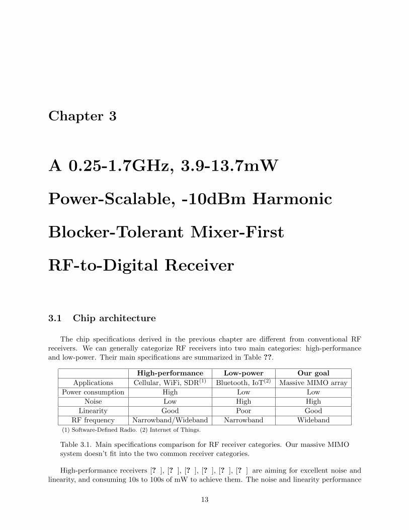
The chip specifications derived in the previous chapter are different from conventional RFreceivers. We can generally categorize RF receivers into two main categories: high-performanceand low-power. Their main specifications are summarized in Table ??.
High-performance Low-power Our goal
Applications Cellular, WiFi, SDR(1) Bluetooth, IoT(2) Massive MIMO array
Power consumption High Low Low
Noise Low High High
Linearity Good Poor Good
RF frequency Narrowband/Wideband Narrowband Wideband
(1) Software-Defined Radio. (2) Internet of Things.
Table 3.1. Main specifications comparison for RF receiver categories. Our massive MIMOsystem doesn’t fit into the two common receiver categories.
High-performance receivers [? ], [? ], [? ], [? ], [? ], [? ] are aiming for excellent noise andlinearity, and consuming 10s to 100s of mW to achieve them. The noise and linearity performance
13

of a high-end single-antenna receiver are crucial to achieve the desired ranges and address intenseinterference scenarios. Thus these DC power budgets are acceptable. These high-performancereceivers are not intended to be used in variable-size, low-power multi-user MIMO radio arrays.The work in [? ] uses spatial filtering in a 4-element array to tolerate large in-band blockers andto relax the dynamic range of the analog-to-digital converter (ADC), but consumes >110 mW tosupport 4 receiver elements without integrated ADCs. In [? ], a multi-antenna system with analogbeamforming is shown, but does not include baseband circuitry and supports only a single user.Neither [? ] nor [? ] supports harmonic rejection, which is needed in wideband RF systems thatcan address multiple frequency bands and communication standards. The work in [? ] shows ahigh-performance single receiver with resiliency to harmonic blockers, but consumes a large amountof power in noise-cancelling circuitry that is not needed in a massive MIMO array. RF receiversfor software-defined radio (SDR) as in [? ] provide only bandwidth and RF frequency tuning, butcannot be configured to trade power for NF in larger MIMO arrays.
Low-power receivers [? ], [? ], [? ] are constrained by strict DC power budgets of a few mW. Tomeet the power budget, these receivers compromise on noise performance (which is acceptable sincethe data rates and ranges are smaller) and linearity (though nowadays interference is becoming moreimportant when the number of IoT devices is sharply increasing). In addition, low-power receiversare narrowband which allows low-power LO generation and distribution schemes.
However, our system does not fit into these categories. We would like to have a receiver withgood linearity (since we use digital beamforming) and low power (due to very large array size),but we can compromise on the noise since it is averaged across the array elements. We would liketo design a programmable noise-power tradeoff as a common element of arrays with varying sizes;as the array size is increased, the relaxed per-element noise requirements are leveraged to reducepower consumption. In addition we would like to support a wideband RF (requiring harmonicrejection) and variable array size/noise specification (a scalable solution). Hence a new receiverarchitecture is needed.
3.1.1 Mixer-first receivers
The first question to address is the RF frond-end. High-performance receivers target very lownoise performance, and usually use a Low Noise Amplifier (LNA) as the first stage of the receiver.The LNA conributes low noise while providing large gain, so the noise contribution of the laterstages is very small. To achieve a low noise performance, the power consumption of the LNA shouldbe relatively large (typically 5-10mW). Moreover, the LNA experiences large blocker swings, andits power consumption should be large enough to sustain large blockers.
In recent years, a mixer-first topology was introduced [? ], which enables noise figures of afew dB-s and excellent out-of-band linearity. The main idea is shown in Figure ??. A switchingmixer is connected directly to the RF port, driven by non-overlapping LO phases. Each switch isshown as an ideal switch and a series resistor Rsw representing the switch series resistance. Onthe base-band side, each mixer is connected to a shunt capacitor CB, and the equivalent resistancefrom the base-band side is represented by RB. Charge-conservation analysis [? ] shows that theinput impedance for our linear time-varying (LTV) system can be accurately represented using alinear time-invariant (LTI) model as shown in Figure ??. γ represents the fundamental harmonic
14

conversion gain:
γ =1
Nsinc2
(1
N
)(3.1)
and Rsh represents the loss due to up-conversion of the baseband voltage via the LO harmonics:
Rsh =Nγ
1−Nγ(Ra +Rsw) (3.2)
where N is the number of the LO phases (N = 4 in Figure ??).
0°
RBCB
Rsw
VRF
0°
90°
270°
Ra
180°
RBCB
Rsw
90°
RBCB
Rsw
270°
RBCB
Rsw
I+
I-
Q+
Q-
180°
Figure 3.1. Mixer-first receiver conceptual diagram (left) and the corresponding LO wave-forms (right). Ra is the antenna resistance, Rsw is the mixer switch resistance, and theswitches are ideal.
γRBRshVRF
Ra+Rsw
Figure 3.2. Mixer-first equivalent Linear Time-Invariant model. Impedance matching isachieved for Rsw + γRB||Rsh = Ra
The mixer-first architecture has two important properties:
• Impedance matching can be achieved by using small switch resistance Rsw and small equiva-lent baseband resistance RB so that Rsw + γRB||Rsh = Ra = 50Ω. For N = 4 we get γ = 0.2and Rsh = 4.3 (Ra +Rsw). Switch resistances of less than 10Ω can easily be implemented us-ing large mixer switch devices in modern processes. Low base-band resistance can be achievedby using Trans-Impedance Amplifiers (TIAs).
15
• Band-pass filter -like input impedance is essentially achieved at RF frequecy due to up-conversion of the base-band impedance. At RF frequencies close to the LO frequency (in-band) we can achieve an impedance match, while at RF frequencies further away from theLO frequency (out-of-band) we see a low impedance (limited by the switch resistance). Thisimpedance profile results in excellent out-of-band linearity of mixer-first receivers.
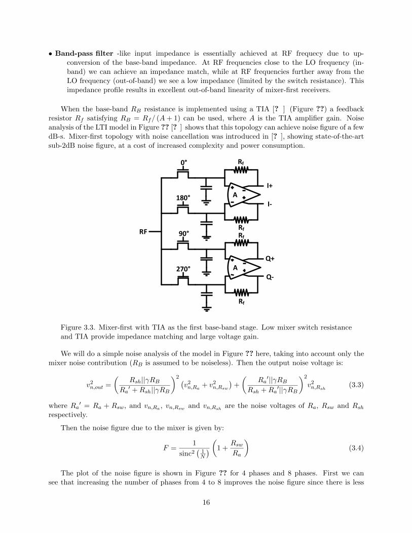
When the base-band RB resistance is implemented using a TIA [? ] (Figure ??) a feedbackresistor Rf satisfying RB = Rf/ (A+ 1) can be used, where A is the TIA amplifier gain. Noiseanalysis of the LTI model in Figure ?? [? ] shows that this topology can achieve noise figure of a fewdB-s. Mixer-first topology with noise cancellation was introduced in [? ], showing state-of-the-artsub-2dB noise figure, at a cost of increased complexity and power consumption.
0°
180°
90°
Rf
A
270°
RF
I+
I-
Rf
Rf
AQ+
Q-
Rf
Figure 3.3. Mixer-first with TIA as the first base-band stage. Low mixer switch resistanceand TIA provide impedance matching and large voltage gain.
We will do a simple noise analysis of the model in Figure ?? here, taking into account only themixer noise contribution (RB is assumed to be noiseless). Then the output noise voltage is:
v2n,out =
(Rsh||γRB
Ra′ +Rsh||γRB
)2 (v2n,Ra
+ v2n,Rsw
)+
(Ra′||γRB
Rsh +Ra′||γRB
)2
v2n,Rsh
(3.3)
where Ra′ = Ra + Rsw, and vn,Ra , vn,Rsw and vn,Rsh
are the noise voltages of Ra, Rsw and Rsh
respectively.
Then the noise figure due to the mixer is given by:
F =1
sinc2(
1N
) (1 +Rsw
Ra
)(3.4)
The plot of the noise figure is shown in Figure ?? for 4 phases and 8 phases. First we cansee that increasing the number of phases from 4 to 8 improves the noise figure since there is less
16

re-radiation to higher harmonics (more on that in the next section). From equation ?? we can
see that this improvement issinc2( 1
8)sinc2( 1
4)= 0.7dB, independent of the switch resistance. This is a
substantial difference when targeting noise figures of a few dB, but less important for our spec.More importantly, even when the switch resistances are as large as several 100s of Ωs (correspondingto minimum switch sizes in modern processes), the mixer noise contribution corresponds to noisefigures of less than 10dB.
The power cost of the small switch resistance for high-performance mixer-first receivers is quitelarge, summarized in Table ??. Since the LO power is consumed by digital gates, the powerconsumption is proportional to the frequency PLO = CV 2f , where C is the total capacitance ofthe LO distribution, V is the LO supply voltage and f is the LO frequency. So it is convenient toconsider the LO power per frequency (mW/GHz). We can see from the table that the LO poweris a substantial part of the total (LO+BB) power. While the base-band power is constant, the LOpower increases with the frequency. So at a few GHz of LO frequency the LO is the dominant partof the total power.
Since the LO power consumption is significant, and we don’t need to use large switches forour noise specifications, we can use switches with large resistance and save substantial LO power.Moreover, since switches are easily scalable, we can build a bank of parallel switches and pick thesize that we need for a desired spec. This architecture will enable us to achieve the noise tuningrange that we need. However, we won’t be able to achieve impedance matching using base-bandTIAs, since the switch resitance will already be larger than 50Ω. We will address this issue insection ??.
0 50 100 150 200 250 300Rsw (+)
0
2
4
6
8
10
NF
(dB
)
N=4N=8
Figure 3.4. Mixer-first noise figure, mixer noise contribution only. Note that even resistancesof several 100s of Ωs provide noise figures of less than 10dB.
17

Ref.Technology
(nm)f (GHz)
Rsw(Ω)
LOphases
NF(dB)
BB power(mW)
LO power(mW/GHz)
[? ] 180 0.1-1.8 NR 4 3.5 24 11
[? ] 28 0.4-3.5 NR 8 2.6 36 16
[? ] 65 0.1-1.5 10 8 6.5 35 13
[? ] 40 0.1-2.7 20 8 1.6 32 17
[? ] 65 0.1-1.2 20 8 4.4 30 28
[? ] 65 0.2-1.2 5 8 3.5 36 33
Table 3.2. LO power consumption of high-performance mixer-first receivers (NR - notreported). The LO power is a substantial part of the receiver, for low switch resistance(< 20Ω) approximately 10-30mW/GHz are consumed by the LO.
3.1.2 Harmonic rejection
Since we are targeting a wideband frequency operating range of 1-6GHz, if we use a 4-phasemixer-first architecture, we will have a problem of harmonic blockers. Due to the fact that theLO is rectangular, RF signals around the odd harmonics of the LO will be also down-converted tobase-band. The even harmonics can be suppressed by using a differential configuration. The 3rdand 5th harmonics are the most important, since for the lower part of the band (1-2GHz) theseharmonics are still in-band (below 6GHz). Thus a mechanism of harmonic rejection is required tomake sure that the receiver is robust against harmonic blockers.
Harmonic rejection was under intense research in the past two decades. The most popularapproach was introduced in [? ], and its concept is shown in Figure ??. The main idea was to use8 LO phases for the mixer switches, and recombine the outputs with the correct coefficients so asine-like equivalent waveform is implemented. Generally speaking, the more LO phases are used,the more harmonics can be cancelled since the effective LO signal is closer to sinusoidal. For 6phases [? ] only the 3rd harmonic is cancelled, for 8 phases [? ], [? ], [? ], [? ], [? ], [? ] the 3rdand 5th are cancelled, and for 16 phases [? ] the odd harmonics up to 13th order can be cancelled.The design complexity and power consumption grows with the number of LO phases, so using morephases has a large cost.
Additional approaches to achieve harmonic rejection were introduced, all trying to emulate asine-like LO using rectangular (digital) pulses. Multi-level LO DAC [? ], LC tank at 4fLO [? ],2-stage recombination with 8 LO phases [? ], using 3rd and 5th LO harmonics with feedforwardcancellation [? ] and using LO pulse-width modulation [? ] are just a few examples. Theseapproaches are targeting high-performance applications and all require large power for an extrahardware to implement the harmonic rejection.
Since low-power receivers are narrowband, they do not use harmonic rejection. So we need tocome up with a low-power harmonic rejection scheme which will still be highly linear. Thus wewould like to use a rectangular LO with a passive mixer for good linearity and come up with alow-power scheme.
In addition, we’d like to be robust against large harmonic blockers of at least -10dBm. Themajority of mixer-first receivers [? ], [? ], [? ], [? ], [? ], [? ], [? ], [? ], [? ], [? ] don’t mentionthe harmonics power and concentrate on the level of the harmonic rejection. The published resultsthat report the harmonics power are shown in Table ??. We can see that the majority of them are
18

-45°
45°
0°
1,3,5,7fLO
1fLO3fLO
5fLO 7fLO
1fLO
7fLO
3fLO
5fLO
1,7fLO
Equivalent LO waveform
RF
Figure 3.5. Conceptual diagram of a harmonic-rejection mixer with 8 LO phases. Equivalentsine-like LO waveform is created when recombining the LO phases with the right coefficients.
reporting harmonic blocker powers of -25dBm to -37dBm. The work in [? ] is dedicated to improvelarge signal harmonic rejection. Their architecture (called “harmonic rejection TIA”) has extracircuitry for large harmonic blocker resiliency with large power consumption of 40-70mW. Ratherthan quoting the harmonic rejection, this paper shows the NF degradation with large harmonics.We will compare our harmonic rejection linearity to this state-of-the-art paper.
Ref.Harmonics
power (dBm)LO
phasesHarmonics
Rejection(dB)
Method
[? ] -30 8 3,5 60,64 RF+BB Gm (2 stages)
[? ] -37 8 3,5 56,56 RF Gm
[? ] -25 8 3,5 75,45 BB Gm
[? ] -30 4 (1) 3,5,7,9 >70 Digital MMSE equalizer
[? ] -10 8 3,5 not reported (2) Harmonic rejection TIA
(1) Two paths are used. (2) Gain and NF degradation due to large harmonic blockers is reported.
Table 3.3. Published harmonic rejection linearity results. Only one work dedicated to largesignal harmonic rejection is able to cancel -10dBm harmonics.
3.1.3 Proposed architecture
Our proposed architecture is shown in Figure ??. To achieve low power harmonic rejection,we can use small mixer switches with large resistance (as we described in section ??) and use 8phases to cancel the 3rd and 5th harmonics. As mentioned in section ??, we won’t be able toachieve impedance matching using base-band TIAs, since the switch resistance will already belarger than 50Ω. Hence we eliminate the base-band TIAs and use the harmonic recombination Gm
stage directly at the base-band input.
To achieve impedance matching we use a shunt resistor Rp at the RF input. This matching
19

strategy is a simple passive solution with no linearity and power consumption downside. Activenegative impedance matching can be further explored, analyzing its noise, linearity and powerconsumption consequenses.
TIA Gm TIA
LO1
LO2
LO8
Gm TIA
LO1
LO2
LO8
gm1
gm2
gm8
IQ
Rp
TIA/higher order filter
Harmonic cancellationHarmonic cancellation
Amplification
Conventional mixer-first Proposed architecture
gm1
gm2
gm8
IQ
TIA/higher order filter
Figure 3.6. Conventional mixer-first [? ] and the proposed architecture. Harmonic recom-bination earlier in the receiver chain enables better linearity of the harmonic cancellation.Impedance matching is achieved by a shunt Rp resistor.
This architecture has a substantial advantage in the harmonic rejection linearity. In theconventional architecture the harmonic blocker is amplified by the TIAs before getting cancelled bythe Gm stage recombination. In the proposed architecture, the harmonic blocker is cancelled rightat the base-band input before any amplification. Hence this architecture is more linear in termsof harmonic rejection - it is capable of cancelling larger blockers without affecting the fundamentalpath.
In order to calculate the required shunt resistor Rp for impedance matching, we can look at themixer-first input impedance without the base-band TIAs. In this case the low-frequency base-bandimpedance is infinite, and the effective base-band impedance is only Rsh (see Figure ??). Fromequations ?? and ?? for N = 8 we get γ = 0.12 and Rsh = 19.8 (Ra +Rsw). Hence the inputimpedance is:
Rin = Rsw +Rsh = Rsw + 19.8 (Ra +Rsw) (3.5)
From equation ?? the input impedance is in the kΩ range, so we need Rp∼= Ra for matching.
To analyze the noise impact of this parallel matching we can use a simple LTI model in Figure ??.Since Rsh >> Rsw we can ignore Rsh for a simpler analysis (which has only 0.2dB of error in thenoise figure). For Rp = Ra the noise figure is:
F = 2 +4Rsw
Ra(3.6)
20

The factor of 2 is due to the noise of Rp = Ra, and the factor of 4 is due to the fact that Rsw isnot in series with Ra, so the noise of Ra is attenuated by Rp before propagating to the base-bandoutput.
We can compare the mixer-only noise figure of the original mixer-first architecture from equation?? to the proposed architecture. The result is shown in Figure ??. The noise figure degradationis between 3dB for small switch resistances and 6dB for large switch resistances. Based on ourdesired noise figure range of about 12-24dB, the mixer noise contribution of this architecture looksreasonable.
RshRpVRF
Ra Rsw
Figure 3.7. Mixer-first with shunt Rp matching equivalent Linear Time-Invariant model(wihout the base-band noise contribution).
0 50 100 150 200 250 300Rsw (+)
0
2
4
6
8
10
12
14
16
NF
(dB
)
N=8, no RpN=8, Rp=Ra
Figure 3.8. Mixer-first noise figure (mixer noise contribution only), shunt Rp noise impact.Degradation of 3-6dB due to Rp is still reasonable for our low-power high-noise application.
3.1.4 AC-coupling
In the proposed architecture in Figure ??, we need to address the issue of different common-mode voltages of the base-band input and the RF. The base-band input is a Gm stage whereoptimum implementation in terms of noise efficiency is a complimentary inverter structure. Thusthe optimum base-band input common-mode voltage is around mid-rail (0.5Vdd). The three possibleoptions for AC/DC coupling of the mixer are shown in Figure ??. DC coupling is the simplest
21
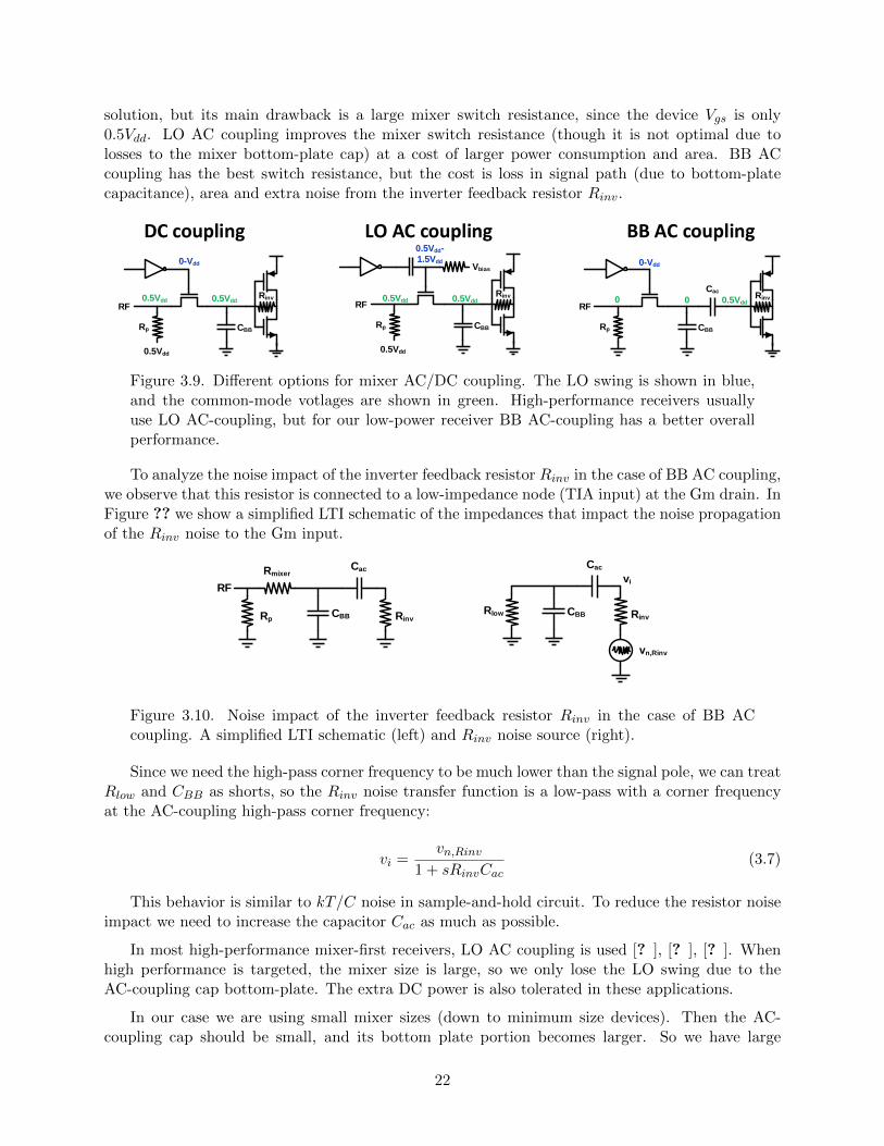
solution, but its main drawback is a large mixer switch resistance, since the device Vgs is only0.5Vdd. LO AC coupling improves the mixer switch resistance (though it is not optimal due tolosses to the mixer bottom-plate cap) at a cost of larger power consumption and area. BB ACcoupling has the best switch resistance, but the cost is loss in signal path (due to bottom-platecapacitance), area and extra noise from the inverter feedback resistor Rinv.
RF
Rp CBB
Rinv
0.5Vdd
0.5Vdd
0-Vdd
DC coupling
RF
Rp CBB
Rinv
Vbias
0.5Vdd
0.5Vdd-
1.5Vdd
0.5VddRF
Rp CBB
CacRinv
0-Vdd
0.5Vdd0
LO AC coupling BB AC coupling
0.5Vdd 0.5Vdd 0
Figure 3.9. Different options for mixer AC/DC coupling. The LO swing is shown in blue,and the common-mode votlages are shown in green. High-performance receivers usuallyuse LO AC-coupling, but for our low-power receiver BB AC-coupling has a better overallperformance.
To analyze the noise impact of the inverter feedback resistor Rinv in the case of BB AC coupling,we observe that this resistor is connected to a low-impedance node (TIA input) at the Gm drain. InFigure ?? we show a simplified LTI schematic of the impedances that impact the noise propagationof the Rinv noise to the Gm input.
RF
Rmixer
CBB
Cac
RinvRpRlow CBB
vi
vn,Rinv
Cac
Rinv
Figure 3.10. Noise impact of the inverter feedback resistor Rinv in the case of BB ACcoupling. A simplified LTI schematic (left) and Rinv noise source (right).
Since we need the high-pass corner frequency to be much lower than the signal pole, we can treatRlow and CBB as shorts, so the Rinv noise transfer function is a low-pass with a corner frequencyat the AC-coupling high-pass corner frequency:
vi =vn,Rinv
1 + sRinvCac(3.7)
This behavior is similar to kT/C noise in sample-and-hold circuit. To reduce the resistor noiseimpact we need to increase the capacitor Cac as much as possible.
In most high-performance mixer-first receivers, LO AC coupling is used [? ], [? ], [? ]. Whenhigh performance is targeted, the mixer size is large, so we only lose the LO swing due to theAC-coupling cap bottom-plate. The extra DC power is also tolerated in these applications.
In our case we are using small mixer sizes (down to minimum size devices). Then the AC-coupling cap should be small, and its bottom plate portion becomes larger. So we have large
22
losses and extra power consumption to drive this bottom-plate cap. Thus we choose to use BBAC-coupling, so we won’t spend extra power on the LO distribution, and pay the extra area andperformance loss of the bottom-plate and noise in the signal path.
3.1.5 DC-offset
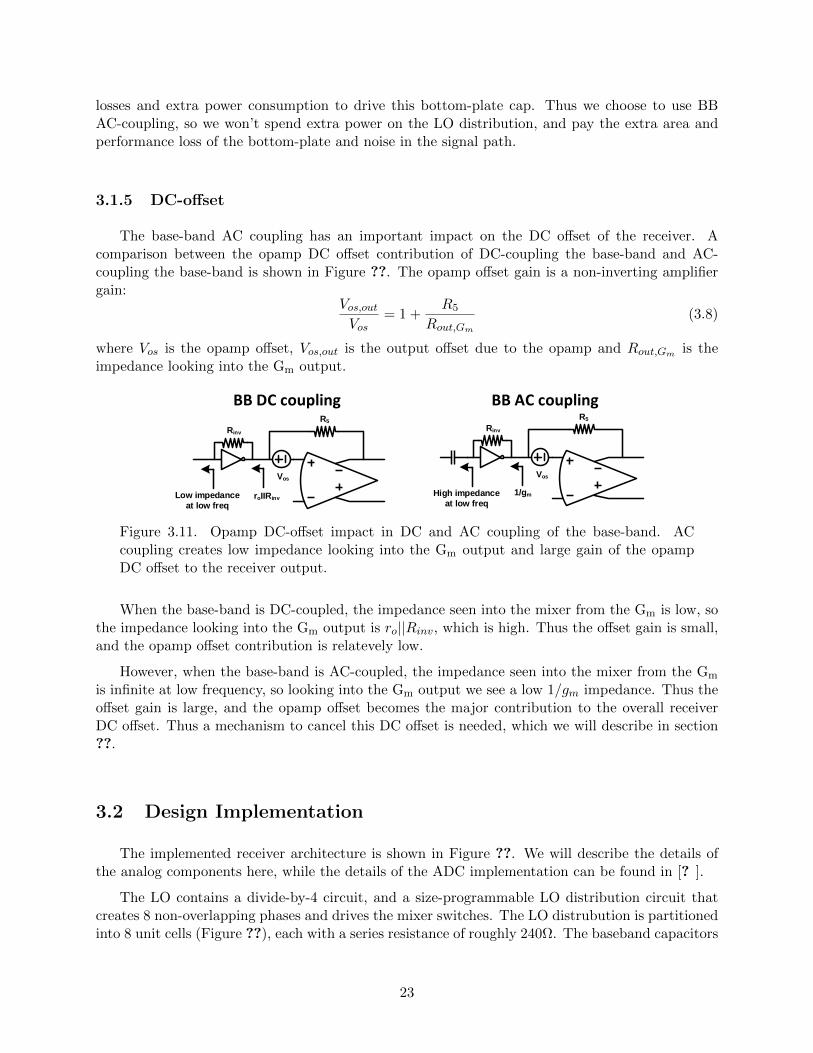
The base-band AC coupling has an important impact on the DC offset of the receiver. Acomparison between the opamp DC offset contribution of DC-coupling the base-band and AC-coupling the base-band is shown in Figure ??. The opamp offset gain is a non-inverting amplifiergain:
Vos,outVos
= 1 +R5
Rout,Gm
(3.8)
where Vos is the opamp offset, Vos,out is the output offset due to the opamp and Rout,Gm is theimpedance looking into the Gm output.
R5
Vos
roIIRinvLow impedance
at low freq
Rinv
R5
Vos
1/gmHigh impedance
at low freq
Rinv
BB AC couplingBB DC coupling
Figure 3.11. Opamp DC-offset impact in DC and AC coupling of the base-band. ACcoupling creates low impedance looking into the Gm output and large gain of the opampDC offset to the receiver output.
When the base-band is DC-coupled, the impedance seen into the mixer from the Gm is low, sothe impedance looking into the Gm output is ro||Rinv, which is high. Thus the offset gain is small,and the opamp offset contribution is relatevely low.
However, when the base-band is AC-coupled, the impedance seen into the mixer from the Gm
is infinite at low frequency, so looking into the Gm output we see a low 1/gm impedance. Thus theoffset gain is large, and the opamp offset becomes the major contribution to the overall receiverDC offset. Thus a mechanism to cancel this DC offset is needed, which we will describe in section??.
3.2 Design Implementation
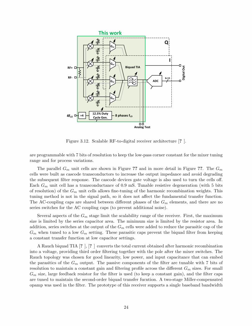
The implemented receiver architecture is shown in Figure ??. We will describe the details ofthe analog components here, while the details of the ADC implementation can be found in [? ].
The LO contains a divide-by-4 circuit, and a size-programmable LO distribution circuit thatcreates 8 non-overlapping phases and drives the mixer switches. The LO distrubution is partitionedinto 8 unit cells (Figure ??), each with a series resistance of roughly 240Ω. The baseband capacitors
23
RF+
RF-
Biquad TIA
6-11
Q
I
Analog Test
Dig
ital
Ou
t
÷44fLO 8 phases fLO
ADC
Gm
12.5% Duty Cycle Gen.
Gm
Gm
Gm
This work
Figure 3.12. Scalable RF-to-digital receiver architecture [? ].
are programmable with 7 bits of resolution to keep the low-pass corner constant for the mixer tuningrange and for process variations.
The parallel Gm unit cells are shown in Figure ?? and in more detail in Figure ??. The Gm
cells were built as cascode transconductors to increase the output impedance and avoid degradingthe subsequent filter response. The cascode devices gate voltage is also used to turn the cells off.Each Gm unit cell has a transconductance of 0.9 mS. Tunable resistive degeneration (with 5 bitsof resolution) of the Gm unit cells allows fine-tuning of the harmonic recombination weights. Thistuning method is not in the signal path, so it does not affect the fundamental transfer function.The AC-coupling caps are shared between different phases of the Gm elements, and there are noseries switches for the AC coupling caps (to prevent additional noise).
Several aspects of the Gm stage limit the scalability range of the receiver. First, the maximumsize is limited by the series capacitor area. The minimum size is limited by the resistor area. Inaddition, series switches at the output of the Gm cells were added to reduce the parasitic cap of theGm when tuned to a low Gm setting. These parasitic caps prevent the biquad filter from keepinga constant transfer function at low capacitor settings.
A Rauch biquad TIA [? ], [? ] converts the total current obtained after harmonic recombinationinto a voltage, providing third order filtering together with the pole after the mixer switches. TheRauch topology was chosen for good linearity, low power, and input capacitance that can embedthe parasitics of the Gm output. The passive components of the filter are tunable with 7 bits ofresolution to maintain a constant gain and filtering profile across the different Gm sizes. For smallGm size, large feedback resistor for the filter is used (to keep a constant gain), and the filter capsare tuned to maintain the second-order biquad transfer fucntion. A two-stage Miller-compensatedopamp was used in the filter. The prototype of this receiver supports a single baseband bandwidth
24

...
...
...
fLO
12.5% Duty CycleGen.
Gm
4x
8x
...
Mixer Unit Cell
RF IN OUT
From duty cycle gen.
Gm Unit Cell
CTLP
BIASN
BIASP
CTLN
IN
OU
T
(single-ended shown)
Scalable Biquad Filter
Figure 3.13. Scalable RF front-end schematic diagram.
6.25pF 1.6MΩ 12.5pF 800kΩ 25pF 400kΩ 3.125pF 3.2MΩ
16841,2
5
5
5
5
5
5
5
5
Figure 3.14. Gm stage schematic diagram. All inputs and outputs are shorted.
25
of 10 MHz, but the architecture can be changed to support various bandwidths for massive MIMOapplications by using higher resolution on the filter capacitors and a higher bandwidth op-amp.
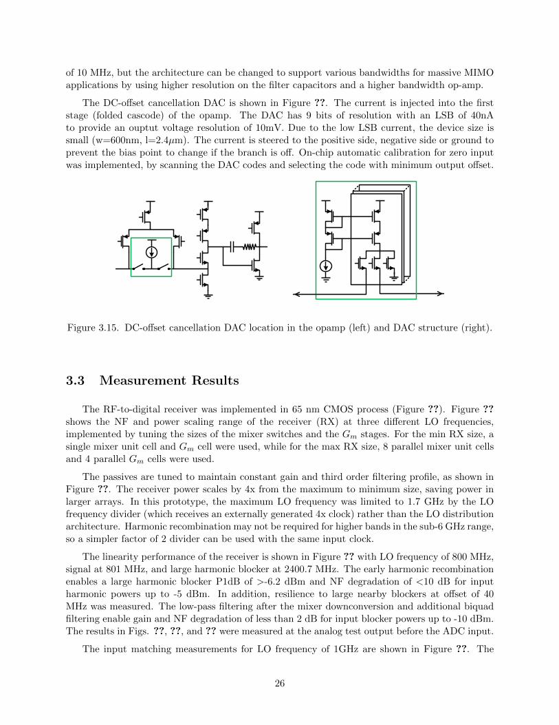
The DC-offset cancellation DAC is shown in Figure ??. The current is injected into the firststage (folded cascode) of the opamp. The DAC has 9 bits of resolution with an LSB of 40nAto provide an ouptut voltage resolution of 10mV. Due to the low LSB current, the device size issmall (w=600nm, l=2.4µm). The current is steered to the positive side, negative side or ground toprevent the bias point to change if the branch is off. On-chip automatic calibration for zero inputwas implemented, by scanning the DAC codes and selecting the code with minimum output offset.
Figure 3.15. DC-offset cancellation DAC location in the opamp (left) and DAC structure (right).
3.3 Measurement Results
The RF-to-digital receiver was implemented in 65 nm CMOS process (Figure ??). Figure ??shows the NF and power scaling range of the receiver (RX) at three different LO frequencies,implemented by tuning the sizes of the mixer switches and the Gm stages. For the min RX size, asingle mixer unit cell and Gm cell were used, while for the max RX size, 8 parallel mixer unit cellsand 4 parallel Gm cells were used.
The passives are tuned to maintain constant gain and third order filtering profile, as shown inFigure ??. The receiver power scales by 4x from the maximum to minimum size, saving power inlarger arrays. In this prototype, the maximum LO frequency was limited to 1.7 GHz by the LOfrequency divider (which receives an externally generated 4x clock) rather than the LO distributionarchitecture. Harmonic recombination may not be required for higher bands in the sub-6 GHz range,so a simpler factor of 2 divider can be used with the same input clock.
The linearity performance of the receiver is shown in Figure ?? with LO frequency of 800 MHz,signal at 801 MHz, and large harmonic blocker at 2400.7 MHz. The early harmonic recombinationenables a large harmonic blocker P1dB of >-6.2 dBm and NF degradation of <10 dB for inputharmonic powers up to -5 dBm. In addition, resilience to large nearby blockers at offset of 40MHz was measured. The low-pass filtering after the mixer downconversion and additional biquadfiltering enable gain and NF degradation of less than 2 dB for input blocker powers up to -10 dBm.The results in Figs. ??, ??, and ?? were measured at the analog test output before the ADC input.
The input matching measurements for LO frequency of 1GHz are shown in Figure ??. The
26

2.1 mm
2.3 mm
RX BB
LO BB
Caps
Figure 3.16. Die micrograph.
Receiver power consumption (mW)5 10 15 20
NF
(d
B)
12
13
14
15
16
17
18
19
20
210.25 GHz1 GHz1.7 GHz
Max RX size
Min RX size
Figure 3.17. Receiver scalability.
Frequency (Hz)10
510
610
7
Ga
in (
dB
)
5
10
15
20
25
30
35
40
45
50
0.25 GHz1 GHz1.7 GHzMaxMin
106
107
43
44
45
46
47
Figure 3.18. Receiver gain for min and max RX size.
27

Ga
in d
eg
rad
atio
n (
dB
)
-8
-6
-4
-2
0
Nearby blocker
Min RX sizeMax RX size
Harmonic blocker
Min RX sizeMax RX size
Blocker power (dBm)-50 -40 -30 -20 -10 0
NF
de
gra
da
tio
n (
dB
)
0
4
8
12Min RX sizeMax RX size
Harmonic blocker power (dBm)
-50 -40 -30 -20 -10 0
Min RX sizeMax RX size
Figure 3.19. Receiver tolerance to 40 MHz offset blocker (left) and in-band 3rd harmonicblocker (right). Measured using an LO frequency of 800 MHz and signal at 801 MHz
impedance seen from the RF port is the intentional 50Ω resistor in parallel with the impedanceseen into the mixer. When the mixer size increases as we approach the min RX size, the out-of-bandimpedance seen into the mixer becomes larger, so the out-of-band impedance seen from the RF portbecomes closer to 50Ω. The center frequency is lower than 1GHz due to the parasitic capacitance ofthe pad and the switches on the RF port. Since the input impedance to the mixer has a band-passresponse, it can be seen as a parallel RLC circuit. Thus adding a parasitic capactance on theRF port decreases the central frequency. Changing the mixer size affects the Q of the band-pass,so the same parasitic capacitance results in different frequency shift. This frequency shift can beeliminated using complex feedback between the base-band I and Q paths [? ], [? ].
0.98 0.99 1 1.01 1.02Frequency (GHz)
-35
-30
-25
-20
-15
-10
-5
0
s11
(dB
)
Min RX sizeMax RX size
Figure 3.20. Measured input matching of the receiver at 1 GHz.
The power consumption breakdown of the receiver and the ADC is shown in Figure ??. The
28

opamp is the only non-scalable part in the current design since its power consumption is rela-tively low. The LO power is the major contributor since we are limited by min size devices whenimplementing the min size RX settings.
LO
8.0mW (58%)
Gm
3.7mW (27%)
Opamp 0.4mW (3%)
ADC
1.6mW (11%)
Max size (13.7 mW total)
LO1.5mW (39%)
Gm
1.0mW (27%)
Opamp0.4mW (11%)
ADC
0.9mW (23%)
Min size (3.9 mW total)
Figure 3.21. Measured power consumption breakdown of the receiver and the ADC at 1 GHz.
3.4 Conclusion
When used in an array, this receiver can be configured with higher NF and lower power asthe number of array elements grows to maintain constant array-level NF and power consumptionwhile improving spatial selectivity. In this work, the single-element NF range is ∼13-19 dB. Foran array-level NF of 1.5 dB, 16 elements are required for the max RX size and 64 elements arerequired for the min RX size. To support >64 elements without linear increase in array power, asmaller (lower power) RX unit cell is required. Similarly, to maintain an array-level NF of 1.5 dBfor <16 elements, more unit cells are required in each receiver to lower the per-element NF.
Figure ?? shows the calculated equivalent array-level NF (bottom) and power consumption (top)for three different LO frequencies. With the proposed scalable architecture, this design can maintainsub-2.5 dB array-level noise figure with up to 64 antennas and <368 mW total receiver+ADC powerconsumption, much lower than any prior art shown in Table ?? when referenced to a 64-elementarray.
While [? ] has relatively low power, it does not include baseband circuitry and uses analogbeamforming that supports only a single user. The harmonic blocker resilience of this scalablelow-power design is comparable to the state-of-the-art [? ], allowing multiple users to be supportedthrough digital beamforming. Overall, this scalable design can support an array size increaseof up to 4x while maintaining excellent linearity and nearly constant array-level NF and powerconsumption.
29

To
tal R
X +
AD
C P
ow
er
(mW
)
0
100
200
300
400
# of Array Elements0 16 32 48 64 80
Arr
ay N
F (
dB
)
0
1
2
3 0.25 GHz1 GHz1.7 GHz
Max sizeRX & ADC
Min sizeRX & ADC
Figure 3.22. Calculated array-level NF and total receiver + ADC power consumption.
[? ] [? ] [? ] [? ]This work
Singleelement
Calculatedarray
performance
RF Freq. (GHz) 0.1-3.1 1.0-2.5 0.1-3.3 0.4-3 0.25-1.7
BW (MHz) NR NR NR 0.5-50 10
Array elements 4 4 1 1 1 8 32
NF (dB)(1) 3.4-5.8(2) 6 1.7 1.8-2.413.2-13.8(3)
18.6-19.3(4) 4.2-4.8 3.5-4.2
Gain (dB) 41 12 NR 70 46
3rd harm. blockerP1dB (dBm)
N/A N/A -6.5 N/A-4.3(3)
-6.2(4) -4.3 -6.2
Harm. blocker NF@-5dBm (dB)
N/A N/A 9 N/A22.9(3)
24.6(4) 13.8 9.6
Out-of-bandIIP3 (dBm)
-5/12(5) 5 11.5 814.6(3)
18.8(4) 14.6 18.8
Supply (V) 1.2 1.0 1.0 0.9 1.2 Analog, 1.0 Digital
CMOS technology 65 nm 65 nm 28 nm 28 nm 65 nm
Total power (mW) 116-147 26-36 36.8-62.4 <407.6-19(3)
3.1-7.6(4) 61-152 99-243
Total area (mm2) 0.8 0.2 5.2 0.6 0.7 5.6 22.4
NR: Not reported. N/A: Not applicable.
(1) For multi-element arrays, equivalent array-level noise figure calculated as
single-element NF - 10 log10(num. of array elements). (2) With spatial filtering enabled (without: 1.7-4.5 dB).
(3) Max size configuration. (4) Min size configuration. (5) Depends on receiving angle.
Table 3.4. Summary and comparison with state-of-the-art.
30

Chapter 4
BAG-Generated RF Receiver for
Large Antenna Arrays
4.1 Motivation
The receiver design that we described in the previous chapter has a fews issues that can beimproved.
First, optimization of the power consumption was not rigorously performed. We came up withthe architecture that enables scalable noise-power consumption tradeoff, but did not design it tohave optimum power consumption for each noise setting.
Second, the design was performed for a particular technology (65nm). Design decisions (likeLO/BB AC coupling, LO chain fanout, Gm stage strurcture and so on) were made for this particulartechnology. If we’d like to design the next version of this receiver in a different technology node, weshould repeat the same manual process of creating schematics, drawing layouts, running simulations,updating schematic and layout parameters all over again. The optimum design point will obviouslydepend on the technology, so we need to have a very long design cycle to get the final optimizeddesign.
This problem is of course nothing new, analog designers faced it for many decades. Recentlya Berkeley Analog Generator version 2 (BAG2) framework was introduced [? ]. This frameworkenables design automation by creating process-portable circuit “generators”. The generators arecapturing the design methodoogy, the schematic and layout creation and running testbenches.Using this framework we can write a single circuit generator for the entire system, and producedifferent implementations (“instances”) for different specs and different technologies.
In section ?? we will give a short introduction of the BAG framework. Then in section ?? wewill introduce a design methodology procedure within BAG that will provide us with the optimumreceiver given the specs and the technology. In section ?? we will give a detailed description of the
31

chip that implements this design methodology in a 16nm FinFET process, and in section ?? wewill show the measurement results.
4.2 Berkeley Analog Generator
The Berkeley Analog Generator (BAG) was first introduced in [? ]. The main idea of thisframework was that instead of designing a circuit for a specific spec and technology, the designershould capture the design methodology into a circuit “generator”. The generator gets inputs ofspecs and technology and consists of methods to produce schematics, layouts and testbenches.Using these generators the designer can implement automated design procedures (including loops)that result in a verified post-layout simulated design that meets the desired specs (an “instance”).This procedure is illustrated in Figure ??. For different specs and/or different technologies, thegenerator can quickly produce different instances, which reduces the overall design time. Recentlya second version of BAG was released [? ], which enables easier process-independent generatorscreation for deeply scaled technologies and has new layout generation engines.
SpecificationsCircuit
Generator
Verified Design Instance• DRC, LVS clean• Meets the specs
Technology
Figure 4.1. The general idea of a generator: a single procedure (circuit generator) producesverified design instance for given specifications and technology.
A simplified flowchart of a circuit generator design is shown in Figure ??. The blocks shownin blue are implemented in the generator framework (Python) and the blocks shown in brown aregenerated into the circuit design and simulation software (Cadence Virtuoso). We can summarizethe steps as follows:
• The design script gets the specifications and the technology as its inputs, and provides theparameters (device sizes, threshold flavors, number of stages etc.) for the schematic, layoutand testbench generators.
• The schematic, layout and testbench generators create an instance according to the parametersspecified by the design script. The generated layout is DRC clean, and passes LVS with thegenerated schematic.
• The generated testbench is executed for the generated circuit (after post-layout extraction).
• The simulated results are fed back into the design script and compared with the desired spec-ifications. If some of the specs are not met and a change of parameters is required, newschematic, layout and testbench instances are generated and the procedure is repeated. Alsoif the specs are met but a more optimized result is required, the procedure can be repeated.
From Figure ?? we can see that four scripts should be written: the three generators (schematic,layout and testbench) and the design script. The design script incorporates the design methodology
32

Schematic Generator
Layout Generator
Schematic
Layout
Testbench
TestbenchGenerator
Simulation Results
Design Script
Figure 4.2. BAG generator design flowchart. The blocks shown in blue are implemented inthe generator framework (Python) and the blocks shown in orange are generated into thecircuit design and simulation software (Cadence Virtuoso)2.
of the circuit. Based on the specs it can select the desired architecture, run preliminary device-levelsimulations (or get them from a previously generated database), run circuit-level simulations forsub-circuits and extract their important parameters in the desired design space and technology, runoptimization algorithms on these parameters (without running additional simulations) and so on.
The flow in Figure ?? is a simplified one, in practice every generator has a different version ofthis flow. Our goal is to create a flow that will minimize the execution time until the specs aremet, so the overall design time is minimized. Thus we should come up with a design methodologythat will minimize the number of generation and simulation cycles.
Another important feature of a BAG generator that it can actually provide us instances withbetter performance than manual designs. If many design iterations are needed, automation savesconsiderable amount of time, since the designer doesn’t need to repeat manual steps of changingthe schematic and the layout and re-running simulations. So with an automated BAG generator,better optimization result can be achieved in shorter overall design time for new specificationsand/or technology.
In addition, generators enable easy design re-use for different projects. Many building blocksare used for different applications, with different specs or technologies. Once a generator is built,it can be used for different projects or for different blocks in the same system, without manuallyre-designing it for each particular application.
2In addition to the generated schematic, layout and testbench, a behavioral model and various other files(lef/lib/verilog/spice/...) need to be generated to enable integration into a larger SoC.
33

4.3 Receiver Design Methodology
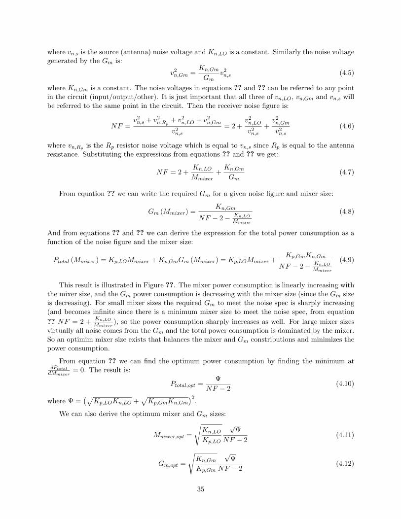
4.3.1 DC power optimization
The first question to address is how should we find the optimum DC power consumption fora given noise figure spec. The main contributors to the noise of the receiver are the front-endcomponents: the Rp matching resistor, the mixer switches and the baseband Gm. They are shownin the schematic in Figure ??. Rp is fixed to be equal to the antenna resistance for impedancematching. The mixer size (and consequently the LO distribution driving it) and the Gm size areunknown for now.
GmRF
Rp
Figure 4.3. The front-end components that contribute to the noise figure of the receiver.While Rp is fixed, many combinations of the mixer and the Gm size result in the same noisefigure.
We can intuitively see the optimization process in the following way. Larger LO size will resultin lower noise figure and larger power consumption. Similarly, larger Gm size will also result inlower noise figure and larger power consumption. So we could achieve the desired noise figureby using large LO and small Gm, or by using small LO and large Gm. Actually there are manycombinations of the mixer and the Gm size that result in the same overall noise figure. From thesecombinations we would like to pick the mixer size and the Gm size that will minimize the overallpower consumption.
To formulate the optimization process we will write the power consumption and the noisecontribution of the mixer and the Gm as functions of their size. The LO power consumption isproportional to the mixer size Mmixer (number of fingers for given finger width and length):
PLO = Kp,LOMmixer (4.1)
where Kp,LO is a constant. Similarly the Gm stage power consumption is proportional to itstransconductance Gm:
PGm = Kp,GmGm (4.2)
where Kp,Gm is a constant. Thus the total power consumption is:
Ptotal = Kp,LOMmixer +Kp,GmGm (4.3)
The noise voltage generated by the LO is:
v2n,LO =
Kn,LO
Mmixerv2n,s (4.4)
34
where vn,s is the source (antenna) noise voltage and Kn,LO is a constant. Similarly the noise voltagegenerated by the Gm is:
v2n,Gm =
Kn,Gm
Gmv2n,s (4.5)
where Kn,Gm is a constant. The noise voltages in equations ?? and ?? can be referred to any pointin the circuit (input/output/other). It is just important that all three of vn,LO, vn,Gm and vn,s willbe referred to the same point in the circuit. Then the receiver noise figure is:
NF =v2n,s + v2
n,Rp+ v2
n,LO + v2n,Gm
v2n,s
= 2 +v2n,LO
v2n,s
+v2n,Gm
v2n,s
(4.6)
where vn,Rp is the Rp resistor noise voltage which is equal to vn,s since Rp is equal to the antennaresistance. Substituting the expressions from equations ?? and ?? we get:
NF = 2 +Kn,LO
Mmixer+Kn,Gm
Gm(4.7)
From equation ?? we can write the required Gm for a given noise figure and mixer size:
Gm (Mmixer) =Kn,Gm
NF − 2− Kn,LO
Mmixer
(4.8)
And from equations ?? and ?? we can derive the expression for the total power consumption as afunction of the noise figure and the mixer size:
Ptotal (Mmixer) = Kp,LOMmixer +Kp,GmGm (Mmixer) = Kp,LOMmixer +Kp,GmKn,Gm
NF − 2− Kn,LO
Mmixer
(4.9)
This result is illustrated in Figure ??. The mixer power consumption is linearly increasing withthe mixer size, and the Gm power consumption is decreasing with the mixer size (since the Gm sizeis decreasing). For small mixer sizes the required Gm to meet the noise spec is sharply increasing(and becomes infinite since there is a minimum mixer size to meet the noise spec, from equation
?? NF = 2 +Kn,LO
Mmixer), so the power consumption sharply increases as well. For large mixer sizes
virtually all noise comes from the Gm and the total power consumption is dominated by the mixer.So an optimim mixer size exists that balances the mixer and Gm constributions and minimizes thepower consumption.
From equation ?? we can find the optimum power consumption by finding the minimum atdPtotaldMmixer
= 0. The result is:
Ptotal,opt =Ψ
NF − 2(4.10)
where Ψ =(√
Kp,LOKn,LO +√Kp,GmKn,Gm
)2.
We can also derive the optimum mixer and Gm sizes:
Mmixer,opt =
√Kn,LO
Kp,LO
√Ψ
NF − 2(4.11)
Gm,opt =
√Kn,Gm
Kp,Gm
√Ψ
NF − 2(4.12)
35

LO Gm Total
Power
Noise , ,2 n LO n Gm
mixer m
C KNF
M G
,LO p LO mixerP C M ,Gm p Gm mP K G
,2 2, ,
n Gmn Gm n s
m
Kv v
G,2 2
, ,n LO
n LO n smixer
Cv v
M
, ,total p LO mixer p Gm mP C M K G
2 2 2 2 2 2, , , , , ,
2 2 2, , ,
2pn s n R n LO n Gm n LO n Gm
n s n s n s
v v v v v vNF
v v v
,
,
,
,
,,,,
2
2p LO mixer
n Gmm mixer
n LO
mixer
n Gmp Gmp Gm mtotal mixe mixe
n LO
mixe
p LOr ir
r
m xer
KK G M
KG M C
NFM
KC
NFC M C
M
MP M
opt
Gm→∞
Mmixer→∞
Mmixer
Power
Figure 4.4. The mixer, Gm and total power consumption for a given noise figure spec. Anoptimum mixer size exists that balances the mixer and Gm constributions and minimizesthe power consumption.
And the optimum mixer and Gm power consumptions:
Pmixer,opt =√Kp,LOKn,LO
√Ψ
NF − 2(4.13)
PGm,opt =√Kp,GmKn,Gm
√Ψ
NF − 2(4.14)
Our first observation is that the optimum total power consumption is determined by a singleconstant Ψ, which incorporates all circuit parameters: architecture, technology, device choices,supply voltages, etc. For a given technology we should find a topology that minimizes Ψ.
A plot of the optimum power consumption vs the desired noise figure is shown in Figure ??. Forlarge noise figure values, the plot is close to an asymptotic Ψ
NF curve, which makes intuitive sense- when the noise can be larger by 3dB, we can spend 2x less power. However, due to the shuntresistor, when the noise figure is smaller than 10dB, the implementation becomes less efficient.When going down from noise figure of 10dB to 4dB the optimum power increases by 16x instead of4x. This is an expected result, since this architecture was chosen when we had large noise figuresin mind.
Lastly, the breakdown of Ψ can tell us if the mixer or the Gm is the dominant source of powerconsumption. From equations ?? and ?? we can see that:
Pmixer,opt
PGm,opt=
√Kp,LOKn,LO√Kp,GmKn,Gm
(4.15)
Recall that Ψ =(√
Kp,LOKn,LO +√Kp,GmKn,Gm
)2and Ptotal,opt = Pmixer,opt + PGm,opt. So if√
Kp,LOKn,LO is much larger than√Kp,GmKn,Gm, the mixer will dominate the total power con-
sumption, and our effort should be to try to reduce the mixer power consumption for the samemixer noise contribution.
36
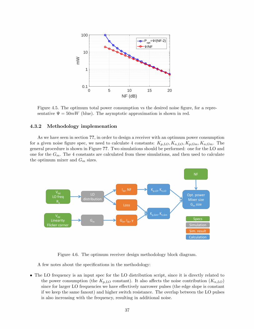
0 5 10 15 20NF (dB)
0.1
1
10
100
mW
Popt
=*/(NF-2)
*/NF
Figure 4.5. The optimum total power consumption vs the desired noise figure, for a repre-sentative Ψ = 50mW (blue). The asymptotic approximation is shown in red.
4.3.2 Methodology implemenation
As we have seen in section ??, in order to design a receiver with an optimum power consumptionfor a given noise figure spec, we need to calculate 4 constants: Kp,LO,Kn,LO,Kp,Gm,Kn,Gm. Thegeneral procedure is shown in Figure ??. Two simulations should be performed: one for the LO andone for the Gm. The 4 constants are calculated from these simulations, and then used to calculatethe optimum mixer and Gm sizes.
VddLO freq
Ra
LO distribution
Idc, NF
NF
Kp,LO, Kn,LO
Specs
Simulation
CalculationSim. result
Gm
Kp,Gm, Kn,GmGm, Idc, γ
Loss
Opt. powerMixer sizeGm size
VddLinearity
Flicker corner
Figure 4.6. The optimum receiver design methodology block diagram.
A few notes about the specifications in the methodology:
• The LO frequency is an input spec for the LO distribution script, since it is directly related tothe power consumption (the Kp,LO constant). It also affects the noise contribution (Kn,LO)since for larger LO frequencies we have effectively narrower pulses (the edge slope is constantif we keep the same fanout) and higher switch resistance. The overlap between the LO pulsesis also increasing with the frequency, resulting in additional noise.
37

• Linearity is only an input to the Gm script, since its V ∗ directly affects it. The mixer linearityis determined by the switch threshold (which is selected to be the lowest for the technologyfor speed reasons) and the supply voltage (which is selected to be highest for speed reasons).
• The flicker corner is an input to the Gm script only, since we are using differential RF and theflicker noise from the LO is rejected as common-mode after down-conversion [? ].
The LO distribution simulation testbench is shown in Figure ??. The matching resistor andthe full 8-phase LO distribution network are included in the testbench. Instead of the actual base-band Gm recombination, an ideal noiseless Verilog-A recombination module is used to produce theequivalent base-band outputs.
RF+
RF-
BB I
BB Q
8-phase
mixer and
LO
distribution
Ideal
recombination
(Verilog-A)
Figure 4.7. The LO testbench for extracting the parameters for the receiver optimization.
From this simulation we get the power consumption and the noise figure for a specific mixersize. Then from equation ??:
Kp,LO =PLO
Mmixer(4.16)
and from equation ?? (without the Gm noise contribution):
Kn,LO = (NF − 2)Mmixer (4.17)
The Gm simulation testbench is shown in Figure ??. A single transcunductor cell is beensimulated.
Gm
Figure 4.8. The Gm testbench for extracting the parameters for the receiver optimization.Large caps are used for transconductance simulation.
From the simulation we get the DC current, transconductance Gm, and input-referred voltagenoise. We can write the power consumption of all Gm cells in the following form:
PGm = Vdd (IGm,I + IGm,Q) = Vdd × 2×(
2 +√
2)× V ∗Gm
2=(
2 +√
2)VddV
∗Gm (4.18)
38
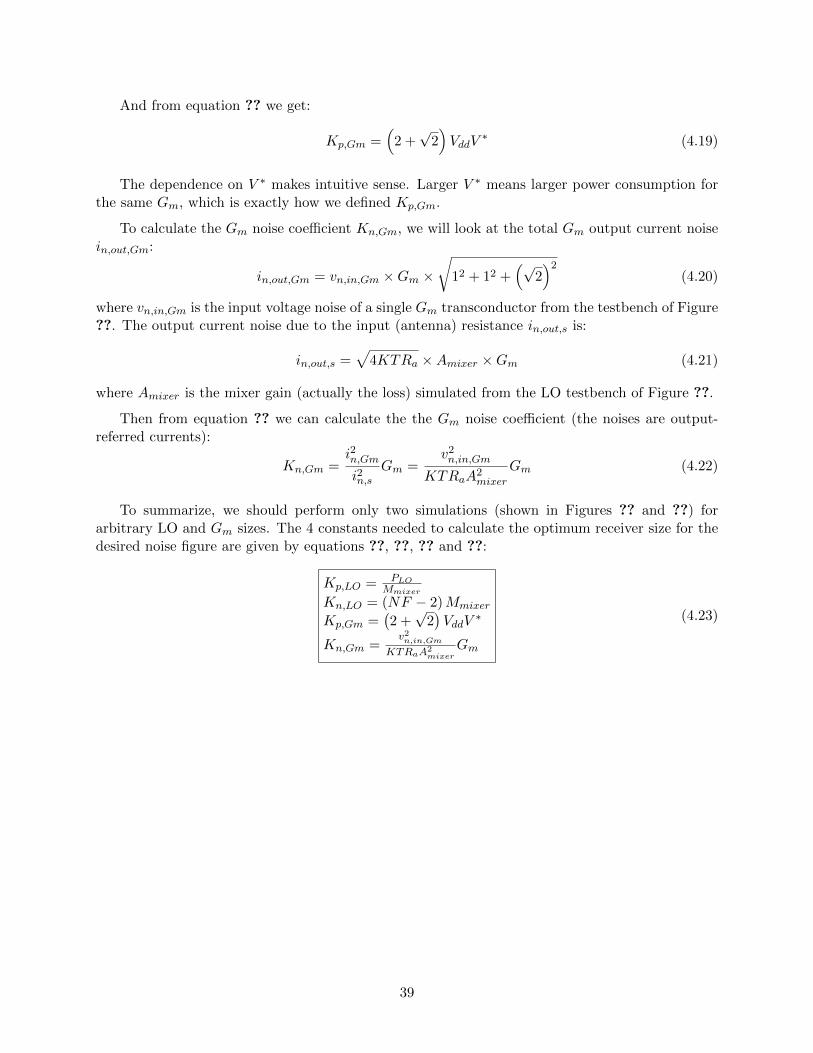
And from equation ?? we get:
Kp,Gm =(
2 +√
2)VddV
∗ (4.19)
The dependence on V ∗ makes intuitive sense. Larger V ∗ means larger power consumption forthe same Gm, which is exactly how we defined Kp,Gm.
To calculate the Gm noise coefficient Kn,Gm, we will look at the total Gm output current noisein,out,Gm:
in,out,Gm = vn,in,Gm ×Gm ×√
12 + 12 +(√
2)2
(4.20)
where vn,in,Gm is the input voltage noise of a single Gm transconductor from the testbench of Figure??. The output current noise due to the input (antenna) resistance in,out,s is:
in,out,s =√
4KTRa ×Amixer ×Gm (4.21)
where Amixer is the mixer gain (actually the loss) simulated from the LO testbench of Figure ??.
Then from equation ?? we can calculate the the Gm noise coefficient (the noises are output-referred currents):
Kn,Gm =i2n,Gm
i2n,sGm =
v2n,in,Gm
KTRaA2mixer
Gm (4.22)
To summarize, we should perform only two simulations (shown in Figures ?? and ??) forarbitrary LO and Gm sizes. The 4 constants needed to calculate the optimum receiver size for thedesired noise figure are given by equations ??, ??, ?? and ??:
Kp,LO = PLOMmixer
Kn,LO = (NF − 2)Mmixer
Kp,Gm =(2 +√
2)VddV
∗
Kn,Gm =v2n,in,Gm
KTRaA2mixer
Gm
(4.23)
39

4.4 Chip Implementation
The LO generation diagram is shown in Figure ??. An off-chip LO signal is amplified and fedinto two separate circuits. One is dividing the LO by 4 and creating 8 non-overlapping phases, andthe other is dividing by 2 and creating 4 non-overlapping phases. Each one of these circuits has areset signal that initiates a timing circuit that starts the divider flip-flops at the right state. Theswitches of the 8 phases and 4 phases mixers are connected in parallel. The parasitic cap of theswitches is not limiting our bandwidth since the switches that we are using are small.
The 8 phases mixer is used for the lower band of the input range (1-2GHz), where harmonicrejection is needed. The 4 phases mixer is used for the higher band of the input range (2-6GHz),where harmonic rejection is not required and we can save power by using less phases. Also thehighest frequency to implement 8 phases is limited by the finite rise and fall times of the LO, soit’s not practical to implement 8 phases at 6GHz (where the input frequency would be 24GHz).
An AC-coupled inverter amplifier is used for an external LO input of 4-12GHz which drivesthe two timing circuits. This architecture can be used with an on-chip LO PLL instead of theexternal LO. Since the input LO is off-chip, the LO receiver is of fixed size, and not optimized toachieve the optimum power consumption for the required noise figure. The LO part included inthe optimization is the timing circuit, the divider, and the logic driving the mixer switches.
:2
:4
8 phases
4 phases
RF
TimingRST8
BB
TimingRST4
LO
Figure 4.9. LO generation block diagram. RST8 and RST4 are reset signals to start the8-phase and 4-phase LO dividers.
A detailed diagram of the timing circuit and the divider-by-4 is shown in Figure ??. Thedifferential divider consists of two divider state machines, one for each phase of the input LO. Eachdivider state machine starts at a fixed state 1000. The timing diagram of the negative clock phaseLON outputs is shown at the bottom (the positive clock phase LOP diagram is similar). The resetsignal starts a LORN clock that drives the dividing registers. The register outputs are NANDedwith the input to create the output pulses that drive the mixers. Since the register ouput pulses are2x wider than the input clock, the NAND output edges are defined by the input clock edges andnot by the register output edges. This way the registers are not contributing noise to the outputpulses. An inverter chain drives the mixer switches. The divider-by-2 has the same timing circuitand two registers instead of four in each divider state machine.
40

LOP
RST8
LON
Timing :4
LOP
LON
RST8
RST8P
RST8N
RST8P
RST8N
LORP
LORN
LORP
LORN
D315
LO315
D270
D180
D225
LO225
D135
LO135
D045
LO045
D090
D000
LO270
LO180
LO090
LO000
LO270 LO180 LO090 LO000
D270 D180 D090 D000
Figure 4.10. LO generation timing circuit and divider-by-4.
41

In section ?? we have analyzed the different options for AC-coupling the mixer. In the firstversion of the chip we chose to use base-band AC-coupling, since the LO overhead power fordriving the bottom-plate of the AC-coupling caps was large. However, the area of the base-bandAC-coupling caps was very large. Now with BAG generation, it is easier to generate differentlayouts and explore the different LO configurations. Also now we are using technology with smallerparasitics (16nm vs 65nm) which can lead to different optimum design.
The simplest way to implement an LO AC-coupling is shown in Figure ??. The LO is passingthrough a high-pass filter formed by a series capacitor and a shunt resistor. The resistor has tobe large enough to prevent the cap from discharging when the mixer gate voltage is high. For asmall switch the mixer cap is a few fF, so the AC-coupling cap is order of 10-s of fF. Our lowestfrequency of operation is 1GHz, so the RC time constant should be at least 5ns. For C = 20fF itleads to R = 250kΩ, which is not practical from an area standpoint.
Vbias
Vbias
Mixer+
Mixer-
Vdd
0
Vlow
Vhigh
0
Vdd
Figure 4.11. Simplest implementation of LO AC-coupling. Large resistor size makes thissolution impractical for small mixer sizes.
A better LO AC-coupling implementation is shown in Figure ??. When the inverter outputgoes high to Vdd, the bias switch is turned off and the mixer gate is charged to Vdd + Vbias. Whenthe inverter ouptut goes low to 0, the bias switch is turned on and the mixer gate is shorted toVbias.
Vbias
Vbias
Mixer+
Mixer-
Vdd
0
0
Vdd
Vbias
Vbias+Vdd
Vbias
Vbias
Mixer-
Vdd
0
Vdd
0
Vbias
Vbias+Vdd
0
Vdd
0
Vdd
Mixer+
Figure 4.12. LO AC-coupling implementation with nmos switches (left) and pmos switches(right).
This technique can be implemented using nmos and pmos switches. For nmos we might have
42
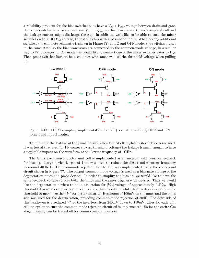
a reliability problem for the bias switches that have a Vdd + Vbias voltage between drain and gate.For pmos switches in off state, we have |Vgs| = Vbias, so the device is not turned completely off andthe leakage current might discharge the cap. In addition, we’d like to be able to turn the mixerswitches on to a DC Vdd voltage, to test the chip with a base-band input. When adding additionalswitches, the complete schematic is shown in Figure ??. In LO and OFF modes the switches are setin the same state, so the bias transistors are connected to the common-mode voltage, in a similarway to ??. However, in ON mode, we would like to connect one of the mixer switches gates to Vdd.Then pmos switches have to be used, since with nmos we lose the threshold voltage when pullingup.
Mixer-
Mixer+
Vdd0
Mixer-
Mixer+
Mixer-
Mixer+
LO mode
0
LO
LO_B
OFF mode
Vdd
Vdd
0
0
Vdd
Vcm
Vcm
Vcm to
Vcm+Vdd
Vcm to
Vcm+Vdd0 to Vdd
0 to Vdd
Vcm
Vcm
0
Vcm
Vcm
Vcm
Vcm
Vcm
ON mode
Vdd
Vdd
0
0
0Vdd
Vcm
Vdd
Vcm
Vdd
Vcm
Vdd 0
Vcm
Vdd 0
Vcm
Vdd
Figure 4.13. LO AC-coupling implementation for LO (normal operation), OFF and ON(base-band input) modes.
To minimize the leakage of the pmos devices when turned off, high-threshold devices are used.It was tested that even for FF corner (lowest threshold voltage) the leakage is small enough to havea negligible impact on the waveform at the lowest frequency of 1GHz.
The Gm stage transconductor unit cell is implemented as an inverter with resistive feedbackfor biasing. Large device length of 1µm was used to reduce the flicker noise corner frequencyto around 400KHz. Common-mode rejection for the Gm was implemented using the conceptualcircuit shown in Figure ??. The output common-mode voltage is used as a bias gate voltage of thedegeneration nmos and pmos devices. In order to simplify the biasing, we would like to have thesame feedback voltage to bias both the nmos and the pmos degeneration devices. Thus we wouldlike the degeneration devices to be in saturation for |Vgs| voltage of approximately 0.5Vdd. Highthreshold degeneration devices are used to allow this operation, while the inverter devices have lowthreshold to maximize their V ∗ for better linearity. Headroom of 100mV on the nmos and the pmosside was used for the degeneration, providing common-mode rejection of 30dB. The downside ofthis headroom is a reduced V ∗ of the inverters, from 240mV down to 150mV. Thus for each unitcell, an option to turn the common-mode rejection circuit off is implemented. So for the entire Gmstage linearity can be traded off for common-mode rejection.
43

IN+ IN-OUT+OUT-
Figure 4.14. Common-mode rejection concept for the Gm stage.
We will now show the simulation results of the methodology to achieve the optimum LO andGm size described in section ??. The following inputs were given to the optimization script:
• Supply voltage of 0.9V for the LO and the Gm.
• LO frequency of 1GHz, 8 phases mixer.
• Antenna impedance of 50Ω.
• Flicker corner of 500KHz. Gm unit cell pre-characterization was performed, resulting in channellength of 1µm.
The simulation results of the 4 constants in the methodology diagram (Figure ??) are shownin Table ??:
Kp,LO (µW) 146
Kn,LO 266
Kp,LOKn,LO (mW) 39
Kp,Gm(V 2) 0.7
Kn,Gm (mS) 37
Kp,GmKn,Gm (mW) 25
Ψ (mW) 126
Table 4.1. Simulation results for mininum power consumption optimization.
Recall that from equation ?? Ψ =(√
Kp,LOKn,LO +√Kp,GmKn,Gm
)2and Ptotal,opt = Ψ
NF−2 .So after calculating Ψ from the LO and Gm characterization we are able to calculate the optimumsizes for a given noise figure spec. These sizes are shown in Table ??. Mmixer is the mixer numberof fingers (nmos device of L=16nm and 2 fins) and MGm is the Gm number of fingers (inverter withL=1µm, 4 fins for nmos and 5 fins for pmos). We can see that when the noise figure is increased by
44

3dB, the LO size, Gm size and total power consumption are decreased by approximately 2x. Theratio is close to 2x for large noise figures and gets larger as the noise figure decreases, as we haveseen in Figure ??.
NF (dB) 12 15 18 21 24
Mmixer 34.6 16.2 7.8 3.9 1.9
Gm (mS) 6.0 2.8 1.4 0.7 0.3
MGm 161.7 75.6 36.7 18.1 9.0
Ptotal (mW) 9.1 4.2 2.1 1.0 0.5
Table 4.2. Optimum LO and Gm sizes vs noise figure spec.
A noise figure of 15dB was chosen for this chip. The choice was practical from the total arearestriction, since we have 4 transceivers in our chip. The optimum power consumption breakdownfor NF=15dB in shown in Figure ??. From the results in Table ?? we see that Kp,LOKn,LO andKp,GmKn,Gm are of the same order of magnitude so the overall power contributions of the LO andthe Gm are similar. The LO power is approximately equally divided between the timing circuit,the divider and the mixers logic and drivers.
Gm1.88mW Timing
0.67mW
Divider0.81mW
Mixers0.86mW
LO2.33mW
Figure 4.15. The simulated power consumption breakdown of the optimum receiver size forNF=15dB.
It is insightful to compare the high-level parameters of the current chip and the previous chip.The comparison is shown in Table ??. In the first generation FADER1 chip (described in chapter??) we have used base-band AC-coupling that made the Gm noise constant Kn,Gm significantlylarger. The Gm power constant Kp,Gm is smaller for the new chip since the supply voltage issmaller (0.9V vs 1.2V). The LO noise and power constants cannot be easily compared since theyare defined with respect to the mixer number of fingers, and a single finger switch performance isvery different in different technologies. For the LO part we can compare the overall LO constantKp,LOKn,LO. We can see that despite the fact that the new chip includes more functionality, as itincludes the LO (timing circuit and divider) and uses LO AC-coupling, the overall LO constant isstill smaller. There are two main reasons to this improvement. First, now we use more advancedtechnolology with smaller devices, smaller parasitics, and lower supply voltage. Second, the designprocess with BAG generation enabled us to generate designs with optimized sizing (such as numberof stages and fanout) due to layout generation automation.
The layout snapshot of the RF part of the chip is shown in Figure ??. The RF part of the chipcontains four transceivers that share the same LO receiver circuit. Each transceiver consists of the
45
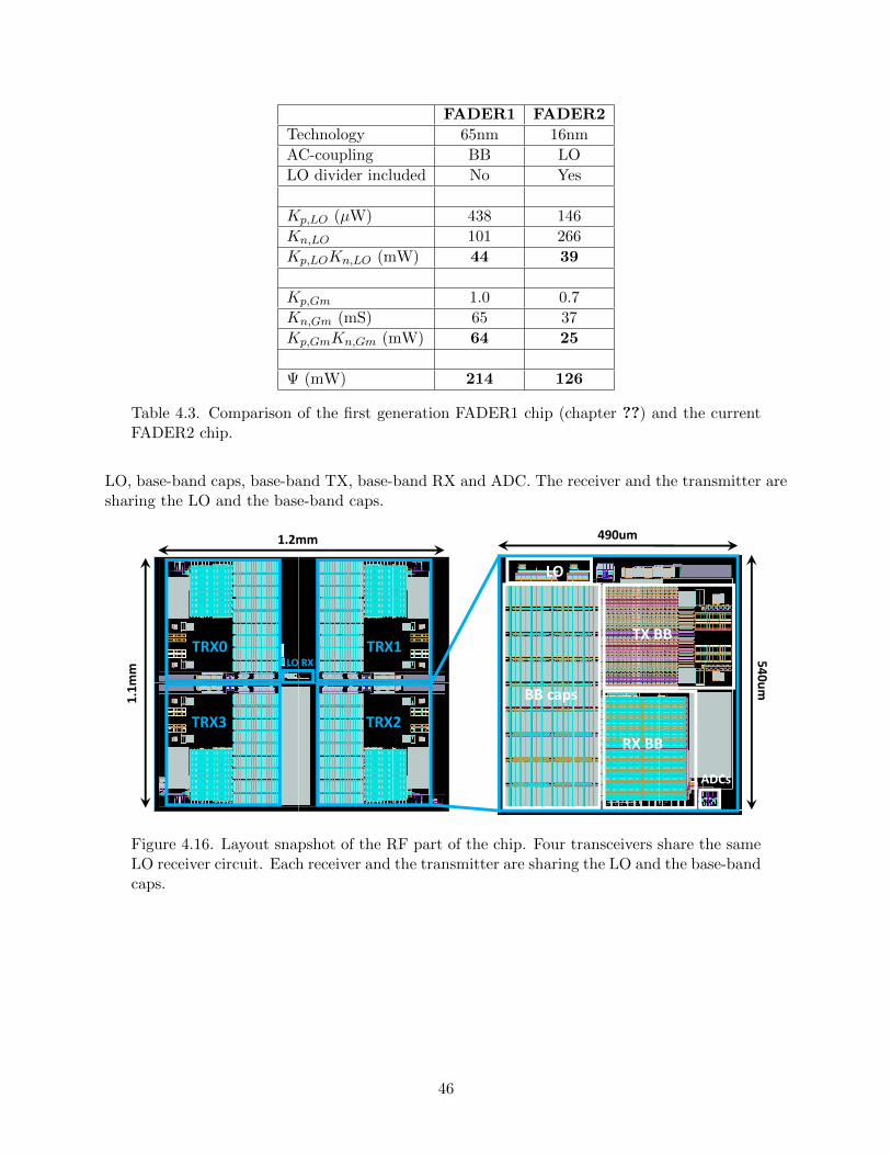
FADER1 FADER2
Technology 65nm 16nm
AC-coupling BB LO
LO divider included No Yes
Kp,LO (µW) 438 146
Kn,LO 101 266
Kp,LOKn,LO (mW) 44 39
Kp,Gm 1.0 0.7
Kn,Gm (mS) 65 37
Kp,GmKn,Gm (mW) 64 25
Ψ (mW) 214 126
Table 4.3. Comparison of the first generation FADER1 chip (chapter ??) and the currentFADER2 chip.
LO, base-band caps, base-band TX, base-band RX and ADC. The receiver and the transmitter aresharing the LO and the base-band caps.
BB caps
LO
TX BB
RX BB
ADCs
490um
540um
TRX2TRX3
TRX1TRX0LO RX
1.2mm
1.1m
m
Figure 4.16. Layout snapshot of the RF part of the chip. Four transceivers share the sameLO receiver circuit. Each receiver and the transmitter are sharing the LO and the base-bandcaps.
46
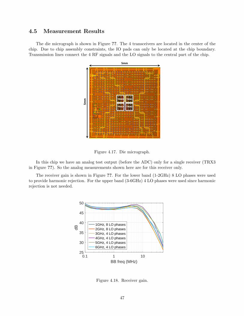
4.5 Measurement Results
The die micrograph is shown in Figure ??. The 4 transceivers are located in the center of thechip. Due to chip assembly constraints, the IO pads can only be located at the chip boundary.Transmission lines connect the 4 RF signals and the LO signals to the central part of the chip.
5mm
5mm TRX1TRX0
TRX2TRX3
Figure 4.17. Die micrograph.
In this chip we have an analog test output (before the ADC) only for a single receiver (TRX3in Figure ??). So the analog measurements shown here are for this receiver only.
The receiver gain is shown in Figure ??. For the lower band (1-2GHz) 8 LO phases were usedto provide harmonic rejection. For the upper band (3-6GHz) 4 LO phases were used since harmonicrejection is not needed.
0.1 1 10BB freq (MHz)
25
30
35
40
45
50
dB
1GHz, 8 LO phases2GHz, 8 LO phases3GHz, 4 LO phases4GHz, 4 LO phases5GHz, 4 LO phases6GHz, 4 LO phases
Figure 4.18. Receiver gain.
47
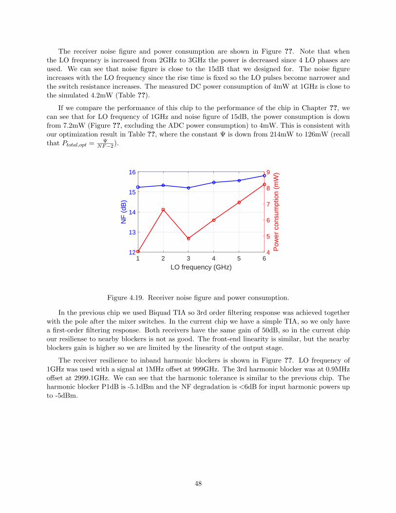
The receiver noise figure and power consumption are shown in Figure ??. Note that whenthe LO frequency is increased from 2GHz to 3GHz the power is decreased since 4 LO phases areused. We can see that noise figure is close to the 15dB that we designed for. The noise figureincreases with the LO frequency since the rise time is fixed so the LO pulses become narrower andthe switch resistance increases. The measured DC power consumption of 4mW at 1GHz is close tothe simulated 4.2mW (Table ??).
If we compare the performance of this chip to the performance of the chip in Chapter ??, wecan see that for LO frequency of 1GHz and noise figure of 15dB, the power consumption is downfrom 7.2mW (Figure ??, excluding the ADC power consumption) to 4mW. This is consistent withour optimization result in Table ??, where the constant Ψ is down from 214mW to 126mW (recallthat Ptotal,opt = Ψ
NF−2).
1 2 3 4 5 6LO frequency (GHz)
12
13
14
15
16
NF
(dB
)
4
5
6
7
8
9
Pow
er c
onsu
mpt
ion
(mW
)
Figure 4.19. Receiver noise figure and power consumption.
In the previous chip we used Biquad TIA so 3rd order filtering response was achieved togetherwith the pole after the mixer switches. In the current chip we have a simple TIA, so we only havea first-order filtering response. Both receivers have the same gain of 50dB, so in the current chipour resiliense to nearby blockers is not as good. The front-end linearity is similar, but the nearbyblockers gain is higher so we are limited by the linearity of the output stage.
The receiver resilience to inband harmonic blockers is shown in Figure ??. LO frequency of1GHz was used with a signal at 1MHz offset at 999GHz. The 3rd harmonic blocker was at 0.9MHzoffset at 2999.1GHz. We can see that the harmonic tolerance is similar to the previous chip. Theharmonic blocker P1dB is -5.1dBm and the NF degradation is <6dB for input harmonic powers upto -5dBm.
48
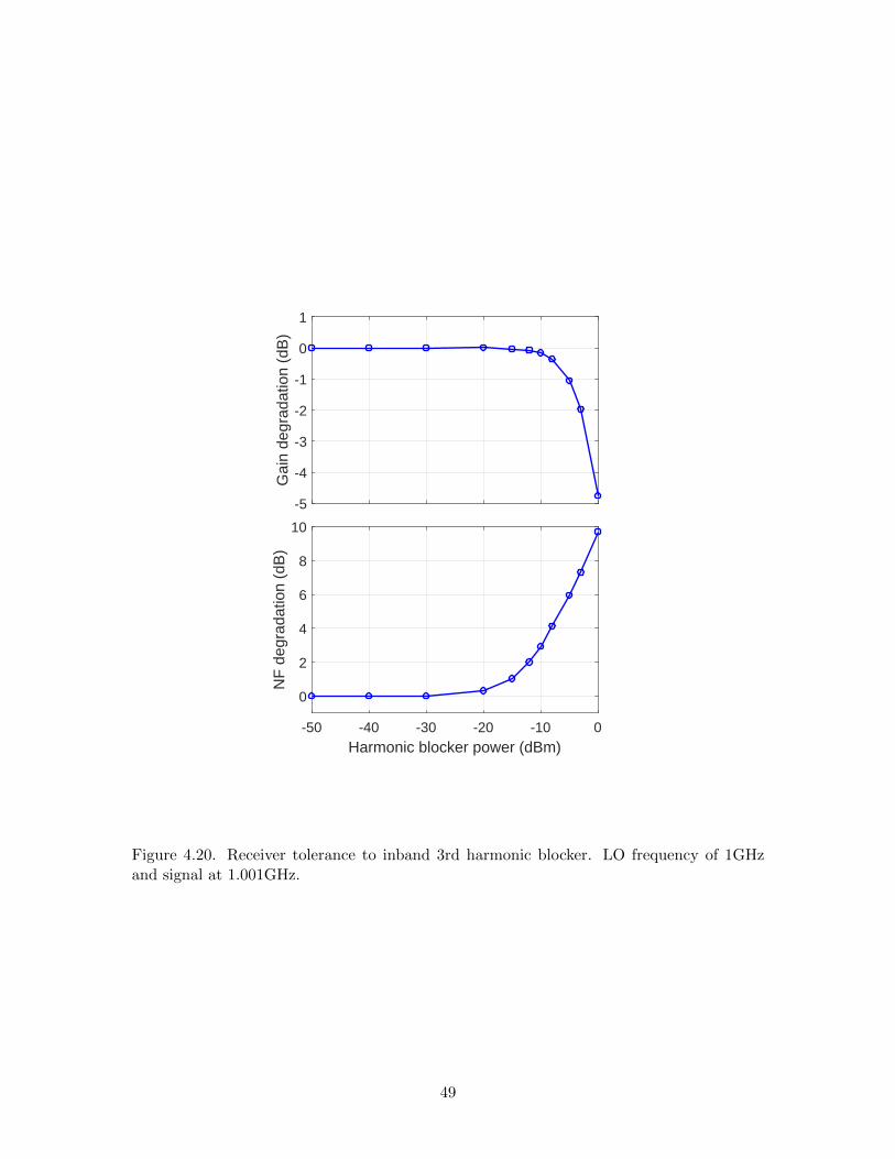
-5
-4
-3
-2
-1
0
1
Gai
n de
grad
atio
n (d
B)
-50 -40 -30 -20 -10 0Harmonic blocker power (dBm)
0
2
4
6
8
10
NF
deg
rada
tion
(dB
)
Figure 4.20. Receiver tolerance to inband 3rd harmonic blocker. LO frequency of 1GHzand signal at 1.001GHz.
49
Chapter 5
Conclusion
5.1 Thesis Summary
This thesis explores RF receivers design for large antenna array systems, with Massive MIMOas a primary application. First, a system analysis is performed, deriving the specifications for thereceiver, with an emphasis on the differences between a large antenna array receiver and a single-antenna receiver. These specifications of low power, high noise and good linearity do not fall in theexisting catagories of “high performance” and “low power” single-antenna receivers.
A new receiver architecture is proposed, where mixer-first receiver with linear baseband chainand early harmonic recombination results in nearby and harmonic blocker tolerance of up to−10dBm. The small size of the mixer switches and the baseband Gm allows us to save powerwhile maintaining good linearity. The architecture has a tunable size of the LO chain and the base-band Gm, so the same receiver can be used in various applications of array sizes and array-levelnoise specifications.
In the first chip prototype, tunable element noise figure results in sub-2.5 dB array-level noisefigure with 16 to 64 antennas and <368 mW total power consumption, for a frequency range of0.25-1.7GHz. Nearby and harmonic blockers of up to -10dBm are tolerated.
In the second chip, Berkeley Analog Generator (BAG) is used to build a circuit generator ofthe receiver. The proposed generator design methodology produces instances with optimum powerconsumption for a given noise figure specification. An instance of this generator is implemented inthe chip, showing power consumption improvement of 50% and wider frequency range of 1-6GHzcompared to the first chip.
50
5.2 Future Work
The design methodology used in the BAG generator has several issues that can be improved.
• The current generator implements a design instance for a single noise specification. Embeddingthe scalability into the design using the approach that we used in the first chip will provide amore complete receiver generator, providing solution to a range of noise figure specifications.Extra power consumption to implement the scalability can be explored and minimized.
• The LO distrubution is now optimized for a single receiver. On the chip we have 4 identicalreceivers and the extra power to drive all 4 is non-negligible. Minimizing this extra power byusing more compact layout where all 4 mixers are closer to each other can help. And takingthis extra power in the power optimization with the baseband Gm will result in a betteroverall power consumption.
• Our power consumption optimization to achieve the desired noise figure does not take the TIApower consumption into account. The TIA power is set by the settling requirements of theADC sampling capacitors. A more complete system level design can be performed that canbalance the ADC resolution/speed and the receiver noise/linearity requirements to achieve alower power consumption of the receiver+ADC.
In addition to the generator methodoogy improvements, on a system level, the beamformingtype can be further explored. In our system we assumed that the digital power consumption won’tbe very large due to relatively low data rates. If this assumption is not true, hybrid beamformingcan be used to reduce the digital power and possibly reduce the RF receiver power due to morerelaxed linearity requirements.
51

Bibliography
[1] “Introduction to LTE Device Testing,” http://http://download.ni.com/evaluation/rf/Introduction to LTE Device Testing.pdf.
[2] C. Andrews and A. C. Molnar, “A passive-mixer-first receiver with baseband-controlled RFimpedance matching, 6dB NF, and 27dBm wideband IIP3,” in 2010 IEEE International Solid-State Circuits Conference - (ISSCC), Feb 2010, pp. 46–47.
[3] K. Trotskovsky, A. Whitcombe, G. Lacaille, A. Puglielli, P. Lu, Z. Wang, N. Narevsky,G. Wright, A. M. Niknejad, B. Nikolic, and E. Alon, “A 0.25-1.7-GHz, 3.9-13.7-mW Power-Scalable, -10-dBm Harmonic Blocker-Tolerant Mixer-First RF-to-Digital Receiver for MassiveMIMO Applications,” IEEE Solid-State Circuits Letters, vol. 1, no. 2, pp. 38–41, Feb 2018.
[4] “Ericsson Mobility Report,” https://www.ericsson.com/en/mobility-report/reports/june-2018, Tech. Rep., June 2018.
[5] “3GPP Releases,” http://www.3gpp.org/specifications/67-releases.
[6] A. M. Niknejad et al., “The xG Vision: Making the Internet truly wireless,” http://files-eu.clickdimensions.com/ericssoncom-anlg4/documents/xg vision 5g public .pdf, 2014.
[7] H. Suzuki, R. Kendall, K. Anderson, A. Grancea, D. Humphrey, J. Pathikulangara,K. Bengston, J. Matthews, and C. Russell, “Highly spectrally efficient Ngara Rural Wire-less Broadband Access Demonstrator,” in 2012 International Symposium on Communicationsand Information Technologies (ISCIT), Oct 2012, pp. 914–919.
[8] C. Shepard, H. Yu, N. Anand, E. Li, T. Marzetta, R. Yang, and L. Zhong, “Argos: PracticalMany-antenna Base Stations,” in Proceedings of the 18th Annual International Conference onMobile Computing and Networking, ser. Mobicom ’12. New York, NY, USA: ACM, 2012, pp.53–64.
[9] C. Shepard, H. Yu, and L. Zhong, “ArgosV2: A Flexible Many-antenna Research Platform,” inProceedings of the 19th Annual International Conference on Mobile Computing & Networking,ser. MobiCom ’13. New York, NY, USA: ACM, 2013, pp. 163–166.
[10] C. W. Shepard, R. Doost-Mohammady, R. E. Guerra, and L. Zhong, “Demo: ArgosV3: AnEfficient Many-Antenna Platform,” in Proceedings of the 23rd Annual International Conferenceon Mobile Computing and Networking, ser. MobiCom ’17. New York, NY, USA: ACM, 2017,pp. 501–503.
[11] J. Vieira, S. Malkowsky, K. Nieman, Z. Miers, N. Kundargi, L. Liu, I. Wong, V. Owall, O. Ed-fors, and F. Tufvesson, “A flexible 100-antenna testbed for Massive MIMO,” in Proceedings ofthe IEEE GLOBECOM Workshops, Dec. 2014, pp. 287–293.
52
[12] “5G Massive MIMO Testbed: From Theory to Reality - National Instruments,” http://www.ni.com/white-paper/52382/en/, last accessed on 09/25/18.
[13] G. Xu, Y. Li, J. Yuan, R. Monroe, S. Rajagopal, S. Ramakrishna, Y. H. Nam, J. Seol, J. Kim,M. M. U. Gul, A. Aziz, and J. Zhang, “Full Dimension MIMO (FD-MIMO): DemonstratingCommercial Feasibility,” IEEE Journal on Selected Areas in Communications, vol. 35, no. 8,pp. 1876–1886, Aug 2017.
[14] A. Puglielli, N. Narevsky, P. Lu, T. Courtade, G. Wright, B. Nikolic, and E. Alon, “A scalablemassive MIMO array architecture based on common modules,” in 2015 IEEE InternationalConference on Communication Workshop (ICCW), June 2015, pp. 1310–1315.
[15] A. Puglielli, A. Townley, G. LaCaille, V. Milovanovic, P. Lu, K. Trotskovsky, A. Whitcombe,N. Narevsky, G. Wright, T. Courtade, E. Alon, B. Nikolic, and A. M. Niknejad, “Design ofEnergy- and Cost-Efficient Massive MIMO Arrays,” Proceedings of the IEEE, vol. 104, no. 3,pp. 586–606, March 2016.
[16] A. Whitcombe, “Configurable Data Converters for Digitally Adaptive Radio,” Ph.D. disserta-tion, EECS Department, University of California, Berkeley, August 2017.
[17] “The LTE Standard,” https://www.qualcomm.com/media/documents/files/the-lte-standard.pdf, Qualcomm Signals Research Group, Tech. Rep., April 2014.
[18] “Introduction to WLAN Testing,” http://download.ni.com/evaluation/rf/Introduction toWLAN Testing.pdf.
[19] J. Borremans, G. Mandal, V. Giannini, B. Debaillie, M. Ingels, T. Sano, B. Verbruggen, andJ. Craninckx, “A 40 nm CMOS 0.4-6 GHz Receiver Resilient to Out-of-Band Blockers,” IEEEJournal of Solid-State Circuits, vol. 46, no. 7, pp. 1659–1671, July 2011.
[20] B. van Liempd, J. Borremans, E. Martens, S. Cha, H. Suys, B. Verbruggen, and J. Craninckx,“A 0.9 V 0.4-6 GHz Harmonic Recombination SDR Receiver in 28 nm CMOS With HR3/HR5and IIP2 Calibration,” IEEE Journal of Solid-State Circuits, vol. 49, no. 8, pp. 1815–1826,Aug 2014.
[21] N. Klemmer, S. Akhtar, V. Srinivasan, P. Litmanen, H. Arora, S. Uppathil, S. Kaylor, A. Ak-our, V. Wang, M. Fares, F. Dulger, A. Frank, D. Ghosh, S. Madhavapeddi, H. Safiri, J. Mehta,A. Jain, H. Choo, E. Zhang, C. Sestok, C. Fernando, R. K.A., S. Ramakrishnan, V. Sinari,and V. Baireddy, “A 45nm CMOS RF-to-Bits LTE/WCDMA FDD/TDD 2x2 MIMO base-station transceiver SoC with 200MHz RF bandwidth,” in 2016 IEEE International Solid-StateCircuits Conference (ISSCC), Jan 2016, pp. 164–165.
[22] “The Effects of Adjacent Channel Rejection and Adjacent Channel Interference on 802.11WLAN Performance,” http://www.ti.com/pdfs/bcg/80211 acr wp.pdf, Texas Instruments,Tech. Rep., November 2003.
[23] L. Zhang and H. Krishnaswamy, “A 0.1-to-3.1GHz 4-element MIMO receiver array support-ing analog/RF arbitrary spatial filtering,” in 2017 IEEE International Solid-State CircuitsConference (ISSCC), Feb 2017, pp. 410–411.
[24] M. C. M. Soer, E. A. M. Klumperink, B. Nauta, and F. E. van Vliet, “3.5 A 1.0-to-2.5GHzbeamforming receiver with constant-Gm vector modulator consuming < 9mW per antenna
53
element in 65nm CMOS,” in 2014 IEEE International Solid-State Circuits Conference Digestof Technical Papers (ISSCC), Feb 2014, pp. 66–67.
[25] D. Murphy, H. Darabi, and H. Xu, “A Noise-Cancelling Receiver Resilient to Large HarmonicBlockers,” IEEE Journal of Solid-State Circuits, vol. 50, no. 6, pp. 1336–1350, June 2015.
[26] S. Kawai, H. Aoyama, R. Ito, Y. Shimizu, M. Ashida, A. Maki, T. Takeuchi, H. Kobayashi,G. Urakawa, H. Hoshino, S. Saigusa, K. Koyama, M. Morita, R. Nihei, D. Goto, M. Na-gata, K. Nakata, K. Ikeuchi, K. Yoshioka, R. Tachibana, M. Arai, C. Teh, A. Suzuki,H. Yoshida, Y. Hagiwara, T. Kato, I. Seto, T. Horiguchi, K. Ban, K. Takahashi, H. Kajihara,T. Yamagishi, Y. Fujimura, K. Horiuchi, K. Nonin, K. Kurose, H. Yamada, K. Taniguchi,M. Sekiya, T. Tomizawa, D. Taki, M. Ikuta, T. Suzuki, Y. Ando, D. Yashima, T. Kaihotsu,H. Mori, K. Nakanishi, T. Kumagaya, Y. Unekawa, T. Aoki, K. Onizuka, and T. Mitomo,“An 802.11ax 44 spectrum-efficient WLAN AP transceiver SoC supporting 1024QAM withfrequency-dependent IQ calibration and integrated interference analyzer,” in 2018 IEEE In-ternational Solid - State Circuits Conference - (ISSCC), Feb 2018, pp. 442–444.
[27] M. Ding, X. Wang, P. Zhang, Y. He, S. Traferro, K. Shibata, M. Song, H. Korpela, K. Ueda,Y. Liu, C. Bachmann, and K. Philips, “A 0.8V 0.8mm2 bluetooth 5/BLE digital-intensivetransceiver with a 2.3mW phase-tracking RX utilizing a hybrid loop filter for interferenceresilience in 40nm CMOS,” in 2018 IEEE International Solid - State Circuits Conference -(ISSCC), Feb 2018, pp. 446–448.
[28] W. Yu, H. Yi, P. Mak, J. Yin, and R. P. Martins, “A 0.18V 382µW bluetooth low-energy(BLE) receiver with 1.33nW sleep power for energy-harvesting applications in 28nm CMOS,”in 2017 IEEE International Solid-State Circuits Conference (ISSCC), Feb 2017, pp. 414–415.
[29] Y. Liu, C. Bachmann, X. Wang, Y. Zhang, A. Ba, B. Busze, M. Ding, P. Harpe, G. vanSchaik, G. Selimis, H. Giesen, J. Gloudemans, A. Sbai, L. Huang, H. Kato, G. Dolmans,K. Philips, and H. de Groot, “A 3.7mW-RX 4.4mW-TX fully integrated Bluetooth Low-Energy/IEEE802.15.4/proprietary SoC with an ADPLL-based fast frequency offset compen-sation in 40nm CMOS,” in 2015 IEEE International Solid-State Circuits Conference - (ISSCC)Digest of Technical Papers, Feb 2015, pp. 1–3.
[30] C. Andrews and A. C. Molnar, “Implications of Passive Mixer Transparency for ImpedanceMatching and Noise Figure in Passive Mixer-First Receivers,” IEEE Transactions on Circuitsand Systems I: Regular Papers, vol. 57, no. 12, pp. 3092–3103, Dec 2010.
[31] D. Murphy, A. Hafez, A. Mirzaei, M. Mikhemar, H. Darabi, M. F. Chang, and A. Abidi, “Ablocker-tolerant wideband noise-cancelling receiver with a 2dB noise figure,” in 2012 IEEEInternational Solid-State Circuits Conference, Feb 2012, pp. 74–76.
[32] H. Hedayati, V. Aparin, and K. Entesari, “A +22dBm IIP3 and 3.5dB NF wideband receiverwith RF and baseband blocker filtering techniques,” in 2014 Symposium on VLSI CircuitsDigest of Technical Papers, June 2014, pp. 1–2.
[33] C. Wu, Y. Wang, B. Nikolic, and C. Hull, “A passive-mixer-first receiver with LO leakagesuppression, 2.6dB NF, >15dBm wide-band IIP3, 66dB IRR supporting non-contiguous carrieraggregation,” in 2015 IEEE Radio Frequency Integrated Circuits Symposium (RFIC), May2015, pp. 155–158.
54

[34] D. Yang and A. Molnar, “A widely tunable active duplexing transceiver with same-channelconcurrent RX/TX and 30dB RX/TX isolation,” in 2014 IEEE Radio Frequency IntegratedCircuits Symposium, June 2014, pp. 321–324.
[35] A. Ghaffari, E. E. A. M. Klumperink, F. v. Vliet, and B. Nauta, “Simultaneous spatial andfrequency-domain filtering at the antenna inputs achieving up to +10dBm out-of-band/beamP1dB,” in 2013 IEEE International Solid-State Circuits Conference Digest of Technical Papers,Feb 2013, pp. 84–85.
[36] J. A. Weldon, R. S. Narayanaswami, J. C. Rudell, L. Lin, M. Otsuka, S. Dedieu, L. Tee,K.-C. Tsai, C.-W. Lee, and P. R. Gray, “A 1.75-GHz highly integrated narrow-band CMOStransmitter with harmonic-rejection mixers,” IEEE Journal of Solid-State Circuits, vol. 36,no. 12, pp. 2003–2015, Dec 2001.
[37] T. Yamaji, J. Matsuno, H. Aoyama, M. Furuta, T. Takida, I. Akita, A. Kuroda, T. Itakura, andN. Itoh, “A 6-phase harmonic rejection down-converter with digital assist,” in 2010 Symposiumon VLSI Circuits, June 2010, pp. 181–182.
[38] T. Forbes, W. Ho, and R. Gharpurey, “Design and Analysis of Harmonic Rejection MixersWith Programmable LO Frequency,” IEEE Journal of Solid-State Circuits, vol. 48, no. 10,pp. 2363–2374, Oct 2013.
[39] A. Maxim, R. Poorfard, M. Reid, J. Kao, C. Thompson, and R. Johnson, “A DDFS DrivenMixing-DAC with Image and Harmonic Rejection Capabilities,” in 2008 IEEE InternationalSolid-State Circuits Conference - Digest of Technical Papers, Feb 2008, pp. 372–621.
[40] I. Fabiano, M. Sosio, A. Liscidini, and R. Castello, “SAW-Less Analog Front-End Receiversfor TDD and FDD,” IEEE Journal of Solid-State Circuits, vol. 48, no. 12, pp. 3067–3079, Dec2013.
[41] Z. Ru, E. A. M. Klumperink, G. J. M. Wienk, and B. Nauta, “A software-defined radioreceiver architecture robust to out-of-band interference,” in 2009 IEEE International Solid-State Circuits Conference - Digest of Technical Papers, Feb 2009, pp. 230–231,231a.
[42] T. Yang, K. Tripurari, H. Krishnaswamy, and P. R. Kinget, “A 0.5GHz-1.5GHz order scalableharmonic rejection mixer,” in 2013 IEEE Radio Frequency Integrated Circuits Symposium(RFIC), June 2013, pp. 411–414.
[43] H. Kang, W. Ho, V. K. Singh, and R. Gharpurey, “A Wideband Receiver Employing PWM-Based Harmonic Rejection Downconversion,” IEEE Journal of Solid-State Circuits, vol. 53,no. 5, pp. 1398–1410, May 2018.
[44] H. Zhang, T. B. Gao, S. C. G. Tan, and O. Shana’a, “A harmonic-rejection mixer with improveddesign algorithm for broadband TV tuners,” in 2012 IEEE Radio Frequency Integrated CircuitsSymposium, June 2012, pp. 163–166.
[45] E. Babakrpur and W. Namgoong, “A 4-phase blocker tolerant wideband receiver with MMSEharmonic rejection equalizer,” in 2016 IEEE Radio Frequency Integrated Circuits Symposium(RFIC), May 2016, pp. 242–245.
[46] M. C. M. Soer, E. A. M. Klumperink, B. Nauta, and F. E. van Vliet, “Spatial InterfererRejection in a Four-Element Beamforming Receiver Front-End With a Switched-Capacitor
55

Vector Modulator,” IEEE Journal of Solid-State Circuits, vol. 46, no. 12, pp. 2933–2942, Dec2011.
[47] V. Giannini, J. Craninckx, S. D’Amico, and A. Baschirotto, “Flexible Baseband Analog Cir-cuits for Software-Defined Radio Front-Ends,” IEEE Journal of Solid-State Circuits, vol. 42,no. 7, pp. 1501–1512, July 2007.
[48] C. Andrews and A. C. Molnar, “A Passive Mixer-First Receiver With Digitally Controlledand Widely Tunable RF Interface,” IEEE Journal of Solid-State Circuits, vol. 45, no. 12, pp.2696–2708, Dec 2010.
[49] E. Chang, J. Han, W. Bae, Z. Wang, N. Narevsky, B. Nikolic, and E. Alon, “BAG2: A process-portable framework for generator-based AMS circuit design,” in 2018 IEEE Custom IntegratedCircuits Conference (CICC), April 2018, pp. 1–8.
[50] J. Crossley, A. Puggelli, H. P. Le, B. Yang, R. Nancollas, K. Jung, L. Kong, N. Narevsky, Y. Lu,N. Sutardja, E. J. An, A. L. Sangiovanni-Vincentelli, and E. Alon, “BAG: A designer-orientedintegrated framework for the development of AMS circuit generators,” in 2013 IEEE/ACMInternational Conference on Computer-Aided Design (ICCAD), Nov 2013, pp. 74–81.
[51] D. Murphy, H. Darabi, A. Abidi, A. A. Hafez, A. Mirzaei, M. Mikhemar, and M. F. Chang,“A Blocker-Tolerant, Noise-Cancelling Receiver Suitable for Wideband Wireless Applications,”IEEE Journal of Solid-State Circuits, vol. 47, no. 12, pp. 2943–2963, Dec 2012.
56