Scalable fabrication of high-quality, ultra-thin single ...
6
Nanoscale PAPER Cite this: Nanoscale, 2016, 8, 6860 Received 25th November 2015, Accepted 1st March 2016 DOI: 10.1039/c5nr08348f www.rsc.org/nanoscale Scalable fabrication of high-quality, ultra-thin single crystal diamond membrane windows† Afaq Habib Piracha, a Kumaravelu Ganesan, a Desmond W. M. Lau, a,b Alastair Stacey, a Liam P. McGuinness, a,c Snjezana Tomljenovic-Hanic a and Steven Prawer* a High quality, ultra-thin single crystal diamond (SCD) membranes that have a thickness in the sub-micron range are of extreme importance as a materials platform for photonics, quantum sensing, nano/micro electro-mechanical systems (N/MEMS) and other diverse applications. However, the scalable fabrication of such thin SCD membranes is a challenging process. In this paper, we demonstrate a new method which enables high quality, large size (∼4 × 4 mm) and low surface roughness, low strain, ultra-thin SCD membranes which can be fabricated without deformations such as breakage, bowing or bending. These membranes are easy to handle making them particularly suitable for fabrication of optical and mechanical devices. We demonstrate arrays of single crystal diamond membranewindows (SCDMW), each up to 1 × 1 mm in dimension and as thin as ∼300 nm, supported by a diamond frame as thick as ∼150 μm. The fabrication method is robust, reproducible, scalable and cost effective. Microwave plasma chemical vapour deposition is used for in situ creation of single nitrogen-vacancy (NV) centers into the thin SCDMW. We have also developed SCD drum head mechanical resonator composed of our fully clamped and freely suspended membranes. 1. Introduction Diamond is well-known for its exceptional mechanical, thermal and optical properties. Diamond is also a high refrac- tive index and wide band gap material which makes it useful in electronic, thermal and optical applications. 1 Single crystal diamond is unique in that it is known to host more than 500 colour centers ranging from ultraviolet (UV) to infrared (IR). 2 Many colour centers are bright enough to be used as single photon sources and some, most notably the negatively charged nitrogen vacancy (NV − ) centre, display a range of highly desir- able quantum properties such as optical single spin read out. Hence, SCD is one of the most promising materials for inte- grated photonics, optomechanics and quantum information processing (QIP) applications. 3,4 In exploiting these properties, many applications in the field of photonics and sensing technologies require high quality thin SCD membranes containing bright colour centres. 4 In particular, for optical waveguide and cavity per- formance, the thickness of the SCD membrane is critical in satisfying the single mode condition in the vertical direction. For applications such as QIP, the thickness of the SCD mem- brane should be on the order of the ratio between the oper- ational vacuum wavelength and the refractive index of the diamond material. 5 In the case of NV − centres for which the zero phonon line wavelength is at 637 nm and the refractive index of diamond material is ∼2.4, the required thickness should be of the order of ∼300 nm. However, macroscopic area, sub-micrometer thick SCD membranes are not commer- cially available. High quality SCD material with macroscopic sizes can be grown only on diamond substrates, although sig- nificant progress is being made with heteroepitaxial growth on silicon via iridium/yttria-stabilized zirconia films. 6,7 Broadly speaking, there are three main approaches developed so far for the production of thin SCD membranes. A conventional process for fabricating thin SCD membranes includes CVD in conjunction with mechanical polishing and chemical etching. 8–16 Recently, SCD plates as thin as ∼5–50 μm have become commercially available. However, further polish- ing and significant RIE thinning is required to achieve the desired sub-micron thicknesses. 8–16 These plates tend to have wedged thickness profiles that result in thickness variations in resultant membranes. 12,13 To date, this has been the most promising approach to fabricate thin SCD membranes and † Electronic supplementary information (ESI) available. See DOI: 10.1039/ c5nr08348f a School of Physics, University of Melbourne, Victoria 3010, Australia. E-mail: [email protected] b ARC Centre of Excellence for Nanoscale BioPhotonics, School of Science, RMIT University, Melbourne, VIC 3001, Australia c Institute for Quantum Optics, University Ulm, Ulm, D-89081, Germany 6860 | Nanoscale, 2016, 8, 6860–6865 This journal is © The Royal Society of Chemistry 2016 Open Access Article. Published on 02 March 2016. Downloaded on 12/13/2021 3:56:46 PM. This article is licensed under a Creative Commons Attribution 3.0 Unported Licence. View Article Online View Journal | View Issue
Transcript of Scalable fabrication of high-quality, ultra-thin single ...

Nanoscale
PAPER
Cite this: Nanoscale, 2016, 8, 6860
Received 25th November 2015,Accepted 1st March 2016
DOI: 10.1039/c5nr08348f
www.rsc.org/nanoscale
Scalable fabrication of high-quality, ultra-thinsingle crystal diamond membrane windows†
Afaq Habib Piracha,a Kumaravelu Ganesan,a Desmond W. M. Lau,a,b Alastair Stacey,a
Liam P. McGuinness,a,c Snjezana Tomljenovic-Hanica and Steven Prawer*a
High quality, ultra-thin single crystal diamond (SCD) membranes that have a thickness in the sub-micron
range are of extreme importance as a materials platform for photonics, quantum sensing, nano/micro
electro-mechanical systems (N/MEMS) and other diverse applications. However, the scalable fabrication
of such thin SCD membranes is a challenging process. In this paper, we demonstrate a new method
which enables high quality, large size (∼4 × 4 mm) and low surface roughness, low strain, ultra-thin SCD
membranes which can be fabricated without deformations such as breakage, bowing or bending. These
membranes are easy to handle making them particularly suitable for fabrication of optical and mechanical
devices. We demonstrate arrays of single crystal diamond membrane windows (SCDMW), each up to 1 × 1 mm
in dimension and as thin as ∼300 nm, supported by a diamond frame as thick as ∼150 µm. The fabrication
method is robust, reproducible, scalable and cost effective. Microwave plasma chemical vapour deposition is
used for in situ creation of single nitrogen-vacancy (NV) centers into the thin SCDMW. We have also developed
SCD drum head mechanical resonator composed of our fully clamped and freely suspended membranes.
1. IntroductionDiamond is well-known for its exceptional mechanical,thermal and optical properties. Diamond is also a high refrac-tive index and wide band gap material which makes it usefulin electronic, thermal and optical applications.1 Single crystaldiamond is unique in that it is known to host more than 500colour centers ranging from ultraviolet (UV) to infrared (IR).2
Many colour centers are bright enough to be used as singlephoton sources and some, most notably the negatively chargednitrogen vacancy (NV−) centre, display a range of highly desir-able quantum properties such as optical single spin read out.Hence, SCD is one of the most promising materials for inte-grated photonics, optomechanics and quantum informationprocessing (QIP) applications.3,4
In exploiting these properties, many applications in thefield of photonics and sensing technologies require highquality thin SCD membranes containing bright colour
centres.4 In particular, for optical waveguide and cavity per-formance, the thickness of the SCD membrane is critical insatisfying the single mode condition in the vertical direction.For applications such as QIP, the thickness of the SCD mem-brane should be on the order of the ratio between the oper-ational vacuum wavelength and the refractive index of thediamond material.5 In the case of NV− centres for which thezero phonon line wavelength is at 637 nm and the refractiveindex of diamond material is ∼2.4, the required thicknessshould be of the order of ∼300 nm. However, macroscopicarea, sub-micrometer thick SCD membranes are not commer-cially available. High quality SCD material with macroscopicsizes can be grown only on diamond substrates, although sig-nificant progress is being made with heteroepitaxial growth onsilicon via iridium/yttria-stabilized zirconia films.6,7 Broadlyspeaking, there are three main approaches developed so far forthe production of thin SCD membranes.
A conventional process for fabricating thin SCD membranesincludes CVD in conjunction with mechanical polishing andchemical etching.8–16 Recently, SCD plates as thin as ∼5–50 µmhave become commercially available. However, further polish-ing and significant RIE thinning is required to achieve thedesired sub-micron thicknesses.8–16 These plates tend to havewedged thickness profiles that result in thickness variations inresultant membranes.12,13 To date, this has been the mostpromising approach to fabricate thin SCD membranes and
†Electronic supplementary information (ESI) available. See DOI: 10.1039/c5nr08348f
aSchool of Physics, University of Melbourne, Victoria 3010, Australia.
E-mail: [email protected] Centre of Excellence for Nanoscale BioPhotonics, School of Science,
RMIT University, Melbourne, VIC 3001, AustraliacInstitute for Quantum Optics, University Ulm, Ulm, D-89081, Germany
6860 | Nanoscale, 2016, 8, 6860–6865 This journal is © The Royal Society of Chemistry 2016
Ope
n A
cces
s A
rtic
le. P
ublis
hed
on 0
2 M
arch
201
6. D
ownl
oade
d on
12/
13/2
021
3:56
:46
PM.
Thi
s ar
ticle
is li
cens
ed u
nder
a C
reat
ive
Com
mon
s A
ttrib
utio
n 3.
0 U
npor
ted
Lic
ence
.
View Article OnlineView Journal | View Issue
employed as a platform for diamond based sensors,8 radiationdetectors,9 micro/nano-mechanical resonators,10–12 integratedphotonics,13,14 Raman lasers15 and frequency combs.16
A different method that has been used is the fabrication of10 µm wide and millimetre long beams with 200 nm thicknessby etching 10 µm deep trenches on a bulk SCD using RIE.17,18
In the last step, thin strips are picked up mechanically fromthe substrate. But, these membranes have not been used forintegrated devices fabrication due to size limitations.
Ion implantation and lift-off is another technique for fabri-cation of free-standing thin SCD membranes.19–22 This tech-nique has many advantages. Prime among these is that ionimplantation process creates an etchable damage layer at a fixeddepth below the surface, and so naturally provides a membraneof uniform thickness that is independent of the parallelism ofthe original substrate. However, the residual damage from theion implantation step introduces built-in strain and alsodegrades the optical quality of the membranes, limiting the useof these membranes for photonic devices.20 These stand-alonethin membranes also tend to crack and bow during lift-off limit-ing the production of large size ultra-thin membranes. Never-theless, CVD overgrowth after ion implantation, can be used toform a high-quality SCD layer followed by plasma etching of thedamaged layer and provides a promising platform for photonicdevice fabrication.21,22 In order to remove the entire damagedregion after CVD overgrowth step, only 1–2 µm of diamondneeds to be removed by RIE. Furthermore, a variety of colourcenters can be incorporated in the membranes through controlof the CVD overgrowth process.23
Each of these methods has their own advantages and dis-advantages. The disadvantages common to all three methodsare the difficulty in handling. To overcome the handlingproblem, these membranes are often bonded to a substratesuch as Si/SiO2 which may restrict the operational functional-ity of membranes due to different thermal/chemical propertiesof the substrate and bonding materials. In addition, scalabilityis another issue to be addressed. Here we report a robustfabrication method that overcomes many of the SCD proces-sing limitations by providing large, ultra-thin, low-strain SCDmembrane windows supported by a thick diamond frame.These membrane window architectures are easy to handlewhile minimizing breakage/curvature and incorporate singleNV centres. The membrane properties are dependent primarilyon control of the CVD overgrowth process, which has beenshown to produce extremely high quality single crystal materialprovided sufficient substrate preparation methods are followedto minimize dislocation generation.24 Furthermore, this fabri-cation process is suitable for large scale production, by allow-ing for parallel implantation, overgrowth and etching ofmultiple membranes.
2. Fabrication
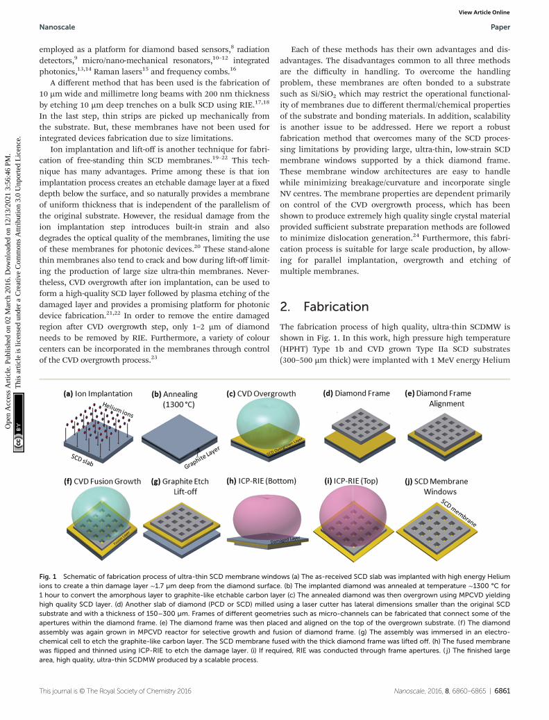
The fabrication process of high quality, ultra-thin SCDMW isshown in Fig. 1. In this work, high pressure high temperature(HPHT) Type 1b and CVD grown Type IIa SCD substrates(300–500 µm thick) were implanted with 1 MeV energy Helium
Fig. 1 Schematic of fabrication process of ultra-thin SCD membrane windows (a) The as-received SCD slab was implanted with high energy Heliumions to create a thin damage layer ∼1.7 µm deep from the diamond surface. (b) The implanted diamond was annealed at temperature ∼1300 °C for1 hour to convert the amorphous layer to graphite-like etchable carbon layer (c) The annealed diamond was then overgrown using MPCVD yieldinghigh quality SCD layer. (d) Another slab of diamond (PCD or SCD) milled using a laser cutter has lateral dimensions smaller than the original SCDsubstrate and with a thickness of 150–300 µm. Frames of different geometries such as micro-channels can be fabricated that connect some of theapertures within the diamond frame. (e) The diamond frame was then placed and aligned on the top of the overgrown substrate. (f ) The diamondassembly was again grown in MPCVD reactor for selective growth and fusion of diamond frame. (g) The assembly was immersed in an electro-chemical cell to etch the graphite-like carbon layer. The SCD membrane fused with the thick diamond frame was lifted off. (h) The fused membranewas flipped and thinned using ICP-RIE to etch the damage layer. (i) If required, RIE was conducted through frame apertures. ( j) The finished largearea, high quality, ultra-thin SCDMW produced by a scalable process.
Nanoscale Paper
This journal is © The Royal Society of Chemistry 2016 Nanoscale, 2016, 8, 6860–6865 | 6861
Ope
n A
cces
s A
rtic
le. P
ublis
hed
on 0
2 M
arch
201
6. D
ownl
oade
d on
12/
13/2
021
3:56
:46
PM.
Thi
s ar
ticle
is li
cens
ed u
nder
a C
reat
ive
Com
mon
s A
ttrib
utio
n 3.
0 U
npor
ted
Lic
ence
.View Article Online

ions with a flux of 5 × 10¹⁶ ions per cm2 to create an end-of-range damage layer at ∼1.7 µm depth from the diamondsurface (Fig. 1a). The end-of-range depth was calculated withStopping and Range of Ions in Matter (SRIM) simulations.25
The implanted substrate was then annealed in vacuum (5 ×10⁻⁶ mbar) at a temperature of ∼1300 °C for 1 hour to convertthe end-of-range sub-surface layer to a graphite-like etchableamorphous carbon layer (Fig. 1b).26,27 The annealed substratewas overgrown using a Cyrannus Iplas microwave plasma chemi-cal vapour deposition (MPCVD) reactor at a growth rate of∼20 nm min−1. The CVD conditions for the high quality homo-epitaxial SCD growth were as follows: microwave power 3000 W,pressure 100 Torr, gas mixture composition 2% methane(CH4) in hydrogen (H2). The substrate temperature was keptbetween 950 °C and 1000 °C (Fig. 1c). A total of 10 sampleswere overgrown to thicknesses ranging between 300 nm and1 µm for use in different experiments. The diamond frameswere fabricated from 150 µm thick diamond slabs (SCD orPCD) using a laser micromachining system (Fig. 1d). Framesof different shapes and geometries can be produced. Thediamond frame was then positioned and aligned to the topsurface of CVD overgrown substrate under an optical micro-scope (Fig. 1e). The lateral dimensions of the frame were∼10% less than that of the substrate with a thickness in therange of 150–300 µm. The frame was temporarily attached tothe top overgrown surface of the substrate by surface tensionand van der Waals forces of the respective diamond materials.The assembly composed of diamond frame and overgrownsubstrate was then placed again in a MPCVD reactor for fusiongrowth under same conditions as shown in Fig. 1c, resultingin selective growth of a new SCD layer through the apertures ofthe frame, and the formation of a fusion layer of diamondmaterial around the contact of the frame and overgrown sub-strate (Fig. 1f). The fused substrate was immersed in a boricacid solution and the graphite-like carbon layer was electro-chemically etched away under constant voltage (∼300 V)applied across two platinum electrodes (Fig. S1 in ESI†). Inthis way, the SCD membrane fused with diamond frame wasseparated and lifted off (Fig. 1g). The fusion was extremelystrong and stable under mechanical force and it survivedharsh chemical and acid treatments.
The membrane fused frame was flipped and the remaining∼1.7 µm damage layer caused by the ion implantation wasremoved using inductive coupled plasma reactive ion etching(ICP-RIE). An alternating sequence based mainly on twoplasma types (Ar/Cl2) and (O2/Ar) was used for etching toachieve high surface quality.28,29 Finally, the surface wentthrough a very mild O2 plasma to etch a few nanometres ofdiamond, preserving the as grown surface.30 RIE was con-ducted until the desired thickness of SCD membrane windowswas achieved (Fig. 1h). Membrane thicknesses were controlledby the RIE thinning rate, while a constant etch rate was con-firmed throughout the process with white light interferometrymeasurement and SEM (see thickness measurement section inESI†). Also, it is important to note that the thickness profile ofthe membrane windows is not affected by RIE within the aper-
tures of diamond frame9 (Fig. 1i), because our techniquerequires the removal of a relatively small thickness of material.Furthermore, an etching step through the diamond frame isnot strictly necessary which may be attractive in some cases. Adiamond cleaning process consisting of acid boiling in amixture of concentrated sulphuric (H2SO4) and sodium nitrate(NaNO3), at high temperature for ∼15 minutes, was performedafter every step of the process to remove any remaining graph-ite residue. This was followed by washing in acetone, methanoland isopropanol to remove surface contamination. Fig. 1jshows the cartoon of final SCDMW fabricated from thismethod. The diamond frame fused to the SCD membrane pro-vided another advantage in preventing cracks and bowingduring lift-off of the membrane and made possible fabricationof millimetre size large membranes. Handling of the SCDmembranes was also manageable, allowing for flipping, trans-ferring and for further processing.
3. Results
Fig. 2 shows the optical, scanning electron microscope (SEM),and atomic force microscope (AFM) micrographs of theSCDMW. Three batches consisting of 10 samples in total werefabricated to demonstrate the scalable and reproduciblenature of fabrication process. Fig. 2(a–c) shows a top downview of the produced arrays of membrane windows. Type Ib(4 × 4 × 0.5 mm) original HPHT SCD substrate was used to fab-ricate 4 × 4 mm large membrane (Fig. 2a) and Type IIa (3 × 3 ×0.3 mm) CVD pristine substrate was diced into 1.5 × 1.5 mm
Fig. 2 (a) Optical micrograph of a large size 4 × 4 mm SCD membraneconsisting of 6 × 6 arrays of membrane windows each with a size 400 ×400 µm connected via thin membrane micro-channels. Each membranewindow can have multiple devices which can be linked via waveguidesin these micro-channels. (b) Optical micrograph of 1.5 × 1.5 mm SCDmembrane containing one large membrane window of size 800 ×800 µm within SCD frame. (c) Optical micrograph of 1.5 × 1.5 mm SCDmembrane having 2 × 2 arrays of membrane windows of size 400 ×400 µm in a diamond frame. (d) SEM image after lift-off showing mem-brane and frame thickness. (e) SEM image of thin membrane windowcross section showing thickness of ∼300 nm and surface quality. (f )AFM scan (5 × 5 µm2) of thin membrane window with root mean square(RMS) surface roughness of ∼3 nm.
Paper Nanoscale
6862 | Nanoscale, 2016, 8, 6860–6865 This journal is © The Royal Society of Chemistry 2016
Ope
n A
cces
s A
rtic
le. P
ublis
hed
on 0
2 M
arch
201
6. D
ownl
oade
d on
12/
13/2
021
3:56
:46
PM.
Thi
s ar
ticle
is li
cens
ed u
nder
a C
reat
ive
Com
mon
s A
ttrib
utio
n 3.
0 U
npor
ted
Lic
ence
.View Article Online
sizes, using laser micromachining to produce membranes of1.5 × 1.5 mm for different experiments (Fig. 2b and c). Featureslike pyramids or pits in the membrane windows are observedfor some samples, which are transferred from original sub-strates during CVD overgrowth step. Membrane surface qualitycan be improved by substrate preparation methods or selectionof smooth and dislocation free substrate.24 Fig. 2(d and e)shows SEM micrographs of the frame side view comprised2 × 2 arrays of membrane windows after lift-off and the crosssectional view confirming the final SCDMW’s thickness of∼300 nm after thinning respectively. AFM scan (5 × 5 µm2)reveals a surface roughness of ∼3 nm (Fig. 2f).
3.1. Raman measurements
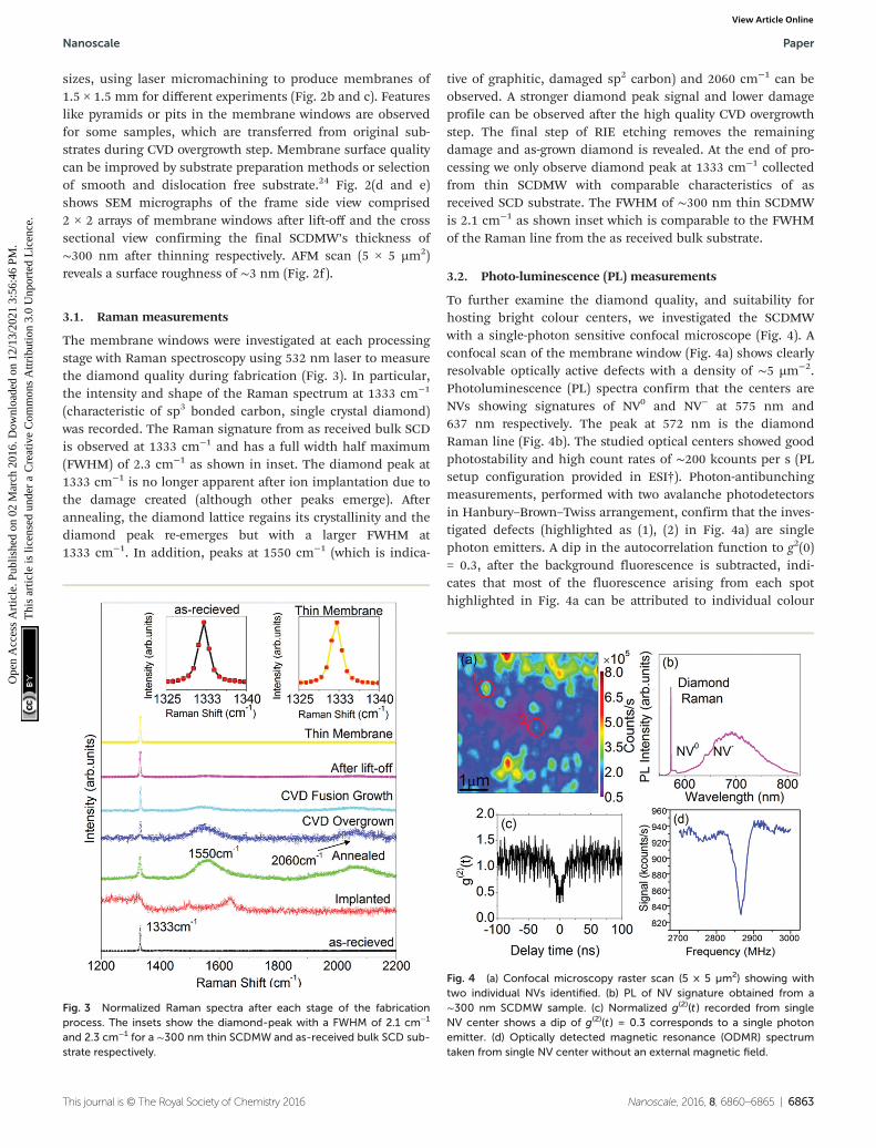
The membrane windows were investigated at each processingstage with Raman spectroscopy using 532 nm laser to measurethe diamond quality during fabrication (Fig. 3). In particular,the intensity and shape of the Raman spectrum at 1333 cm−1
(characteristic of sp3 bonded carbon, single crystal diamond)was recorded. The Raman signature from as received bulk SCDis observed at 1333 cm−1 and has a full width half maximum(FWHM) of 2.3 cm−1 as shown in inset. The diamond peak at1333 cm−1 is no longer apparent after ion implantation due tothe damage created (although other peaks emerge). Afterannealing, the diamond lattice regains its crystallinity and thediamond peak re-emerges but with a larger FWHM at1333 cm−1. In addition, peaks at 1550 cm−1 (which is indica-
tive of graphitic, damaged sp2 carbon) and 2060 cm−1 can beobserved. A stronger diamond peak signal and lower damageprofile can be observed after the high quality CVD overgrowthstep. The final step of RIE etching removes the remainingdamage and as-grown diamond is revealed. At the end of pro-cessing we only observe diamond peak at 1333 cm−1 collectedfrom thin SCDMW with comparable characteristics of asreceived SCD substrate. The FWHM of ∼300 nm thin SCDMWis 2.1 cm−1 as shown inset which is comparable to the FWHMof the Raman line from the as received bulk substrate.
3.2. Photo-luminescence (PL) measurements
To further examine the diamond quality, and suitability forhosting bright colour centers, we investigated the SCDMWwith a single-photon sensitive confocal microscope (Fig. 4). Aconfocal scan of the membrane window (Fig. 4a) shows clearlyresolvable optically active defects with a density of ∼5 µm−2.Photoluminescence (PL) spectra confirm that the centers areNVs showing signatures of NV0 and NV− at 575 nm and637 nm respectively. The peak at 572 nm is the diamondRaman line (Fig. 4b). The studied optical centers showed goodphotostability and high count rates of ∼200 kcounts per s (PLsetup configuration provided in ESI†). Photon-antibunchingmeasurements, performed with two avalanche photodetectorsin Hanbury–Brown–Twiss arrangement, confirm that the inves-tigated defects (highlighted as (1), (2) in Fig. 4a) are singlephoton emitters. A dip in the autocorrelation function to g2(0)= 0.3, after the background fluorescence is subtracted, indi-cates that most of the fluorescence arising from each spothighlighted in Fig. 4a can be attributed to individual colour
Fig. 3 Normalized Raman spectra after each stage of the fabricationprocess. The insets show the diamond-peak with a FWHM of 2.1 cm−1
and 2.3 cm−1 for a ∼300 nm thin SCDMW and as-received bulk SCD sub-strate respectively.
Fig. 4 (a) Confocal microscopy raster scan (5 × 5 µm2) showing withtwo individual NVs identified. (b) PL of NV signature obtained from a∼300 nm SCDMW sample. (c) Normalized g(2)(t ) recorded from singleNV center shows a dip of g(2)(t ) = 0.3 corresponds to a single photonemitter. (d) Optically detected magnetic resonance (ODMR) spectrumtaken from single NV center without an external magnetic field.
Nanoscale Paper
This journal is © The Royal Society of Chemistry 2016 Nanoscale, 2016, 8, 6860–6865 | 6863
Ope
n A
cces
s A
rtic
le. P
ublis
hed
on 0
2 M
arch
201
6. D
ownl
oade
d on
12/
13/2
021
3:56
:46
PM.
Thi
s ar
ticle
is li
cens
ed u
nder
a C
reat
ive
Com
mon
s A
ttrib
utio
n 3.
0 U
npor
ted
Lic
ence
.View Article Online

centers (Fig. 4c). We observe optically detected magnetic reson-ance (ODMR) from a single NV center (marked in Fig. 4a)without external magnetic field as shown in Fig. 4d. There isno peak splitting in the ODMR signal, which suggests thatthere is low strain in the membrane.
3.3. Mechanical resonator measurements
In Fig. 5 we show laser Doppler vibrometer measurements ofthe drumhead mechanical resonator which is composed of afully clamped and freely suspended SCD membrane. We useda ∼1 µm thick SCD membrane window supported by ∼150 µmthick PCD frame. The membrane was clamped in a square geo-metry of side length (L = 400 µm) as shown in Fig. 2(c). Weobserve higher order resonant modes at frequencies measuredapproximately 2 and 3 times ( f12 and f22 respectively) the fun-damental frequency ( f11 ∼ 247 kHz) by mechanically drivingthe membrane with piezoelectric actuation and monitoringthe position response of the membrane optically. These peaks( f12 and f22) correspond to the second and third ordermeasured modes (Fig. 5b). In this experiment, the resonancefrequency response of thin SCDMW was measured in air withlaser Doppler vibrometery at room temperature. This is ingood agreement with the expected values of 200 kHz ( f11),360 kHz ( f21 ∼ 1.8f11) and 578 kHz ( f22 ∼ 2.9f11) predicted for asquare membrane clamped on all sides using Coventor simu-lations. The simulation was performed for a fully clampeddiamond membrane resonator model given thickness = 1 µm,surface area = 400 × 400 µm and material density = 3500 kgm−3. A mechanical quality factor (Q) of ∼400 is achieved in airat a measured fundamental frequency ( f11) of 247 kHz whichis twice that of fully clamped single layer graphene resona-tors31 and also comparable to the Q of 230 for short free stand-ing diamond cantilevers of frequency 6.7 MHz measured in
air.10 The estimated resonant mode shapes at fundamental fre-quency ( f11 ∼ 200 kHz) and third harmonic ( f22 ∼ 578 kHz) isshown respectively (Fig. 5a and c). We observe comparableresonant mode shapes in the membrane at the measured fre-quencies. The resonant mode shape measured at third harmo-nic ( f22 ∼ 740 kHz) is shown in Fig. 5(d).
4. Conclusion
In conclusion, we have presented a scalable method to fabri-cate ultra-thin, large area, high-quality SCDMW with optically-active colour centres. The method is used for successful fabri-cation of robust, large size, ultra-thin membranes fused to athick diamond frame that enables easy handling of the mem-brane, allowing flipping, transferring and further processing.The Raman signature obtained from SCDMW shows high crys-tallinity and low strain. The SCDMW also hosts NV− centerswith single photon emission. The fully clamped and freely sus-pended thin SCDMW displays drum head resonances with a Qof ∼400 in air. The scalable production of high qualitySCDMW opens great prospects as a platform for on-chipdevices for integrated photonics, quantum information proces-sing and sensing devices.
Acknowledgements
This work was funded under the Australian Research Council(ARC) Linkage project (LP100100524) with industry partnersHewlett-Packard Laboratories and ARC Discovery Project (DP1096288). S.T-H. is supported by an ARC Australian ResearchFellowship (DP1096288). L.P.M is supported by the DAADP.R.I.M.E. fellowship. This work was performed in part at theMelbourne Centre for Nanofabrication (MCN) in the VictorianNode of the Australian National Fabrication Facility (ANFF).The authors would like to thank Duc Huynh for assistancewith Coventor simulations.
References
1 R. S. Balmer, J. R. Brandon, S. L. Clewes, H. K. Dhillon,J. M. Dodson, I. Friel, P. N. Inglis, T. D. Madgwick,M. L. Markham, T. P. Mollart, N. Perkins, G. A. Scarsbrook,D. J. Twitchen, A. J. Whitehead, J. J. Wilman andS. M. Woollard, J. Phys.: Condens. Matter, 2009, 21, 364221.
2 A. M. Zaitsev, Optical Properties of a Diamond, Springer,Berlin, 2001.
3 I. Aharonovich, A. D. Greentree and S. Prawer, Nat. Photo-nics, 2011, 5, 397–405.
4 A. Faraon, P. E. Barclay, C. Santori, K. M. C. Fu andR. G. Beausoleil, Nat. Photonics, 2011, 5, 301.
5 S. Tomljenovic-Hanic, M. J. Steel, C. Martijn de Sterke andJ. Salzman, Opt. Express, 2006, 14, 3556.
6 S. Gsell, T. Bauer, J. Goldfuß, M. Schreck and B. Stritzker,Appl. Phys. Lett., 2004, 84, 4541.
Fig. 5 SCD mechanical resonator (a) simulation of resonance of 1 µmthick fully clamped square SCD membrane window at estimated funda-mental frequency 200 kHz. (b) Spectrum of all measured fundamental( f11) and higher modes ( f12 and f12) for the SCDMW. The inset showsmeasured fundamental frequency of membrane with Q ∼400. (c) Thesimulation of resonant mode shapes at estimated third harmonic578 kHz in a diamond membrane. (d) Measured resonant mode shapeof vibrations in the SCDMW observed at experimental third harmonic740 kHz in air using laser Doppler vibrometery at room temperature.
Paper Nanoscale
6864 | Nanoscale, 2016, 8, 6860–6865 This journal is © The Royal Society of Chemistry 2016
Ope
n A
cces
s A
rtic
le. P
ublis
hed
on 0
2 M
arch
201
6. D
ownl
oade
d on
12/
13/2
021
3:56
:46
PM.
Thi
s ar
ticle
is li
cens
ed u
nder
a C
reat
ive
Com
mon
s A
ttrib
utio
n 3.
0 U
npor
ted
Lic
ence
.View Article Online
7 J. Riedrich-Moller, L. Kipfstuhl, C. Hepp, E. Neu, C. Pauly,F. Mucklich, A. Baur, M. Wandt, S. Wolff, M. Fischer,S. Gsell, M. Schreck and C. Becher, Nat. Nanotechnol., 2012,7, 69.
8 P. Maletinsky, S. Hong, M. S. Grinolds, B. Hausmann,M. D. Lukin, R. L. Walsworth, M. Loncar and A. Yacoby,Nat. Nanotechnol., 2012, 7, 320–324.
9 M. Pomorski, B. Caylar and P. Bergonzo, Appl. Phys. Lett.,2013, 103, 112106.
10 J. Teissier, A. Barfuss, P. Appel, E. Neu and P. Maletinsky,Phys. Rev. Lett., 2014, 113, 020503.
11 P. Ovartchaiyapong, L. M. A. Pascal, B. A. Myers, P. Lauriaand A. C. B. Jayich, Appl. Phys. Lett., 2012, 101, 163505.
12 Y. Tao and C. Degen, Adv. Mater., 2013, 25, 3962.13 B. J. M. Hausmann, B. Shields, Q. M. Quan, P. Maletinsky,
M. McCutcheon, J. T. Choy, T. M. Babinec, A. Kubanek,A. Yacoby, M. D. Lukin and M. Loncar, Nano Lett., 2012, 12,1578.
14 A. Faraon, C. Santori, Z. H. Huang, K.-M. C. Fu,V. M. Acosta, D. Fattal and R. G. Beausoleil, New J. Phys.,2013, 15, 025010.
15 P. Latawiec, V. Venkataraman, M. J. Burek,B. J. M. Hausmann, I. Bulu and M. Lončar, Optica, 2015, 2,924–928.
16 B. J. M. Hausmann, I. Bulu, V. Venkataraman, P. Deotareand M. Loncar, Nat. Photonics, 2014, 8, 369.
17 J. S. Hodges, L. Li, M. Lu, E. H. Chen, M. E. Trusheim,S. Allegri, X. Yao, O. Gaathon, H. Bakhru and D. Englund,New J. Phys., 2012, 14, 093004.
18 O. Gaathon, J. S. Hodges, E. H. Chen, L. Li, S. Bakhru,H. Bakhru, D. Englund and R. M. Osgood Jr., Opt. Mater.,2013, 35, 361.
19 B. A. Fairchild, P. Olivero, S. Rubanov, A. D. Greentree,F. WaIdermann, R. A. Taylor, I. Walmsley, J. M. Smith,
S. Huntington, B. C. Gibson, D. N. Jamieson and S. Prawer,Adv. Mater., 2008, 20, 4793.
20 A. Magyar, J. C. Lee, A. M. Limarga, I. Aharonovich, F. Rol,D. R. Clarke, M. B. Huang and E. L. Hu, Appl. Phys. Lett.,2011, 99, 081913.
21 J. C. Lee, A. P. Magyar, D. O. Bracher, I. Aharonovich andE. L. Hu, Diamond Relat. Mater., 2013, 33, 45.
22 I. Aharonovich, J. C. Lee, A. P. Magyar, B. B. Buckley,C. G. Yale, D. D. Awschalom and E. L. Hu, Adv. Mater.,2012, 24, OP54.
23 J. C. Lee, I. Aharonovich, A. P. Magyar, F. Rol and E. L. Hu,Opt. Express, 2012, 20, 8891.
24 I. Friel, S. L. Clewes, H. K. Dhillon, N. Perkins,D. J. Twitchen and G. A. Scarsbrook, Diamond Relat. Mater.,2008, 18, 808–815.
25 J. F. Ziegler, Nucl. Instrum. Methods Phys. Res., Sect. B, 2004,219–220, 1027.
26 N. R. Parikh, J. D. Hunn, E. McGucken, M. L. Swanson,C. W. White, R. A. Rudder, D. P. Malta, J. B. Posthill andR. J. Markunas, Appl. Phys. Lett., 1992, 61, 3124.
27 C. Uzan-Saguy, C. Cytermann, R. Brener, V. Richter,M. Shaanan and R. Kalish, Appl. Phys. Lett., 1995, 67,1194.
28 C. L. Lee, E. Gu, M. D. Dawson, I. Friel andG. A. Scarsbrook, Diamond Relat. Mater., 2008, 17, 1292.
29 C. L. Lee, E. Gu and M. D. Dawson, Diamond Relat. Mater.,2007, 16, 944.
30 F. Fávaro de Oliveira, S. A. Momenzadeh, Y. Wang,M. Konuma, M. Markham, A. M. Edmonds, A. Denisenkoand J. Wrachtrup, 2015, arXiv preprint, arXiv:1507.00890.
31 A. M. Zande, R. A. Barton, J. S. Alden, C. S. Ruiz-Vargas,W. S. Whitney, P. H. Pham, J. Park, J. M. Parpia,H. G. Craighead and P. L. McEuen, Nano Lett., 2010, 10,4869–4873.
Nanoscale Paper
This journal is © The Royal Society of Chemistry 2016 Nanoscale, 2016, 8, 6860–6865 | 6865
Ope
n A
cces
s A
rtic
le. P
ublis
hed
on 0
2 M
arch
201
6. D
ownl
oade
d on
12/
13/2
021
3:56
:46
PM.
Thi
s ar
ticle
is li
cens
ed u
nder
a C
reat
ive
Com
mon
s A
ttrib
utio
n 3.
0 U
npor
ted
Lic
ence
.View Article Online