SBAS095C MAY 2002 14-Bit, 165MSPS DIGITAL-TO-ANALOG CONVERTER · dac904 dac904 14-bit, 165msps...
24
DAC904 DAC904 14-Bit, 165MSPS DIGITAL-TO-ANALOG CONVERTER FEATURES ● SINGLE +5V OR +3V OPERATION ● HIGH SFDR: 20MHz Output at 100MSPS: 64dBc ● LOW GLITCH: 3pV-s ● LOW POWER: 170mW at +5V ● INTERNAL REFERENCE: Optional Ext. Reference Adjustable Full-Scale Range Multiplying Option APPLICATIONS ● COMMUNICATION TRANSMIT CHANNELS WLL, Cellular Base Station Digital Microwave Links Cable Modems ● WAVEFORM GENERATION Direct Digital Synthesis (DDS) Arbitrary Waveform Generation (ARB) ● MEDICAL/ULTRASOUND ● HIGH-SPEED INSTRUMENTATION AND CONTROL ● VIDEO, DIGITAL TV DESCRIPTION The DAC904 is a high-speed, Digital-to-Analog Converter (DAC) offering a 14-bit resolution option within the family of high- performance converters. Featuring pin compatibility among fam- ily members, the DAC908, DAC900, and DAC902 provide a component selection option to an 8-, 10-, and 12-bit resolution, respectively. All models within this family of DACs support update rates in excess of 165MSPS with excellent dynamic performance, and are especially suited to fulfill the demands of a variety of applications. The advanced segmentation architecture of the DAC904 is optimized to provide a high Spurious-Free Dynamic Range (SFDR) for single-tone, as well as for multi-tone signals— essential when used for the transmit signal path of communica- tion systems. The DAC904 has a high impedance (200kΩ) current output with a nominal range of 20mA and an output compliance of up to 1.25V. The differential outputs allow for both a differential or single-ended analog signal interface. The close matching of the current outputs ensures superior dynamic performance in the differential configuration, which can be implemented with a transformer. Utilizing a small geometry CMOS process, the monolithic DAC904 can be operated on a wide, single-supply range of +2.7V to +5.5V. Its low power consumption allows for use in portable and battery-operated systems. Further optimization can be realized by lowering the output current with the adjustable full-scale option. For noncontinuous operation of the DAC904, a power-down mode results in only 45mW of standby power. The DAC904 comes with an integrated 1.24V bandgap refer- ence and edge-triggered input latches, offering a complete converter solution. Both +3V and +5V CMOS logic families can be interfaced to the DAC904. The reference structure of the DAC904 allows for additional flexibility by utilizing the on-chip reference, or applying an external reference. The full-scale output current can be adjusted over a span of 2-20mA, with one external resistor, while main- taining the specified dynamic performance. The DAC904 is available in SO-28 and TSSOP-28 packages. Current Sources LSB Switches Segmented Switches +1.24V Ref. Latches 14-Bit Data Input D13...D0 DAC904 FSA BW +V D +V A AGND CLK DGND REF IN INT/EXT I OUT I OUT BYP PD DAC904 SBAS095C – MAY 2002 www.ti.com Copyright © 2002, Texas Instruments Incorporated Please be aware that an important notice concerning availability, standard warranty, and use in critical applications of Texas Instruments semiconductor products and disclaimers thereto appears at the end of this data sheet. PRODUCTION DATA information is current as of publication date. Products conform to specifications per the terms of Texas Instruments standard warranty. Production processing does not necessarily include testing of all parameters.
Transcript of SBAS095C MAY 2002 14-Bit, 165MSPS DIGITAL-TO-ANALOG CONVERTER · dac904 dac904 14-bit, 165msps...
DAC904
DAC904
14-Bit, 165MSPS DIGITAL-TO-ANALOG CONVERTER
FEATURES SINGLE +5V OR +3V OPERATION
HIGH SFDR: 20MHz Output at 100MSPS: 64dBc
LOW GLITCH: 3pV-s
LOW POWER: 170mW at +5V
INTERNAL REFERENCE:Optional Ext. ReferenceAdjustable Full-Scale RangeMultiplying Option
APPLICATIONS COMMUNICATION TRANSMIT CHANNELS
WLL, Cellular Base StationDigital Microwave LinksCable Modems
WAVEFORM GENERATION
Direct Digital Synthesis (DDS)Arbitrary Waveform Generation (ARB)
MEDICAL/ULTRASOUND
HIGH-SPEED INSTRUMENTATION ANDCONTROL
VIDEO, DIGITAL TV
DESCRIPTIONThe DAC904 is a high-speed, Digital-to-Analog Converter (DAC)offering a 14-bit resolution option within the family of high-performance converters. Featuring pin compatibility among fam-ily members, the DAC908, DAC900, and DAC902 provide acomponent selection option to an 8-, 10-, and 12-bit resolution,respectively. All models within this family of DACs supportupdate rates in excess of 165MSPS with excellent dynamicperformance, and are especially suited to fulfill the demands ofa variety of applications.
The advanced segmentation architecture of the DAC904 isoptimized to provide a high Spurious-Free Dynamic Range(SFDR) for single-tone, as well as for multi-tone signals—essential when used for the transmit signal path of communica-tion systems.
The DAC904 has a high impedance (200kΩ) current output witha nominal range of 20mA and an output compliance of up to1.25V. The differential outputs allow for both a differential orsingle-ended analog signal interface. The close matching of thecurrent outputs ensures superior dynamic performance in thedifferential configuration, which can be implemented with atransformer.
Utilizing a small geometry CMOS process, the monolithic DAC904can be operated on a wide, single-supply range of +2.7V to+5.5V. Its low power consumption allows for use in portable and
battery-operated systems. Further optimization can be realizedby lowering the output current with the adjustable full-scaleoption.
For noncontinuous operation of the DAC904, a power-downmode results in only 45mW of standby power.
The DAC904 comes with an integrated 1.24V bandgap refer-ence and edge-triggered input latches, offering a completeconverter solution. Both +3V and +5V CMOS logic families canbe interfaced to the DAC904.
The reference structure of the DAC904 allows for additionalflexibility by utilizing the on-chip reference, or applying anexternal reference. The full-scale output current can be adjustedover a span of 2-20mA, with one external resistor, while main-taining the specified dynamic performance.
The DAC904 is available in SO-28 and TSSOP-28 packages.
CurrentSources
LSBSwitches
SegmentedSwitches
+1.24V Ref.
Latches
14-Bit Data Input
D13...D0
DAC904
FSA
BW +VD+VA
AGND CLK DGND
REFIN
INT/EXT
IOUT
IOUT
BYP
PD
DAC904
SBAS095C – MAY 2002
www.ti.com
Copyright © 2002, Texas Instruments Incorporated
Please be aware that an important notice concerning availability, standard warranty, and use in critical applications ofTexas Instruments semiconductor products and disclaimers thereto appears at the end of this data sheet.
PRODUCTION DATA information is current as of publication date.Products conform to specifications per the terms of Texas Instrumentsstandard warranty. Production processing does not necessarily includetesting of all parameters.
DAC9042SBAS095Cwww.ti.com
ELECTRICAL CHARACTERISTICSAt T
A = full specified temperature range, +V
A = +5V, +V
D = +5V, differential transformer coupled output, 50Ω doubly terminated, unless otherwise specified.
DAC904U, E
PARAMETER CONDITIONS MIN TYP MAX UNITS
RESOLUTION 14 Bits
OUTPUT UPDATE RATE 2.7V to 3.3V 125 165 MSPSOutput Update Rate (fCLOCK) 4.5V to 5.5V 165 200 MSPSFull Specified Temperature Range, Operating Ambient, TA –40 +85 °C
STATIC ACCURACY(1) TA = +25°CDifferential Nonlinearity (DNL) fCLOCK = 25MSPS, fOUT = 1.0MHz ±2.5 LSBIntegral Nonlinearity (INL) ±3.0 LSB
DYNAMIC PERFORMANCE TA = +25°CSpurious-Free Dynamic Range (SFDR) To Nyquist
fOUT = 1.0MHz, fCLOCK = 25MSPS 72 79 dBcfOUT = 2.1MHz, fCLOCK = 50MSPS 76 dBcfOUT = 5.04MHz, fCLOCK = 50MSPS 68 dBcfOUT = 5.04MHz, fCLOCK = 100MSPS 68 dBcfOUT = 20.2MHz, fCLOCK = 100MSPS 64 dBcfOUT = 25.3MHz, fCLOCK = 125MSPS 60 dBcfOUT = 41.5MHz, fCLOCK = 125MSPS 55 dBcfOUT = 27.4MHz, fCLOCK = 165MSPS 60 dBcfOUT = 54.8MHz, fCLOCK = 165MSPS 55 dBc
Spurious-Free Dynamic Range within a WindowfOUT = 5.04MHz, fCLOCK = 50MSPS 2MHz Span 82 dBcfOUT = 5.04MHz, fCLOCK = 100MSPS 4MHz Span 82 dBc
Total Harmonic Distortion (THD)fOUT = 2.1MHz, fCLOCK = 50MSPS –75 dBcfOUT = 2.1MHz, fCLOCK = 125MSPS –74 dBc
Two TonefOUT1 = 13.5MHz, fOUT2 = 14.5MHz, fCLOCK = 100MSPS 63 dBc
ELECTROSTATICDISCHARGE SENSITIVITY
This integrated circuit can be damaged by ESD. Texas Instru-ments recommends that all integrated circuits be handled withappropriate precautions. Failure to observe proper handlingand installation procedures can cause damage.
ESD damage can range from subtle performance degradationto complete device failure. Precision integrated circuits may bemore susceptible to damage because very small parametricchanges could cause the device not to meet its publishedspecifications.
DEMO BOARDPRODUCT ORDERING NUMBER COMMENT
DAC904U DEM-DAC90xU Populated evaluation board without DAC. Order sample of desired DAC90x model separately.DAC904E DEM-DAC904E Populated evaluation board including the DAC904E.
DEMO BOARD ORDERING INFORMATION
ABSOLUTE MAXIMUM RATINGS
+VA to AGND ......................................................................... –0.3V to +6V+VD to DGND ........................................................................ –0.3V to +6VAGND to DGND ................................................................. –0.3V to +0.3V+VA to +VD ............................................................................... –6V to +6VCLK, PD to DGND ....................................................... –0.3V to VD + 0.3VD0-D13 to DGND ......................................................... –0.3V to VD + 0.3VIOUT, IOUT to AGND .......................................................... –1V to VA + 0.3VBW, BYP to AGND ....................................................... –0.3V to VA + 0.3VREFIN, FSA to AGND ................................................... –0.3V to VA + 0.3VINT/EXT to AGND ........................................................ –0.3V to VA + 0.3VJunction Temperature .................................................................... +150°CCase Temperature ......................................................................... +100°CStorage Temperature ..................................................................... +125°C
SPECIFIEDPACKAGE TEMPERATURE PACKAGE ORDERING TRANSPORT
PRODUCT PACKAGE-LEAD DESIGNATOR(1) RANGE MARKING NUMBER MEDIA, QUANTITY
DAC904U SO-28 DW –40°C to +85°C DAC904U DAC904U Rails, 28" " " " " DAC904U/1K Tape and Reel, 1000
DAC904E TSSOP-28 PW –40°C to +85°C DAC904E DAC904E Rails, 52" " " " " DAC904E/2K5 Tape and Reel, 2500
NOTE: (1) For the most current specifications and package information, refer to our web site at www.ti.com.
PACKAGE/ORDERING INFORMATION

DAC904 3SBAS095C www.ti.com
ELECTRICAL CHARACTERISTICS (Cont.)At TA = +25°C, +VA = +5V, +VD = +5V, differential transformer coupled output, 50Ω doubly terminated, unless otherwise specified.
DAC904U, E
PARAMETER CONDITIONS MIN TYP MAX UNITS
DYNAMIC PERFORMANCE (Cont.)Output Settling Time(2) to 0.1% 30 nsOutput Rise Time(2) 10% to 90% 2 nsOutput Fall Time(2) 10% to 90% 2 nsGlitch Impulse 3 pV-s
DC-ACCURACYFull-Scale Output Range(3)(FSR) All Bits HIGH, IOUT 2.0 20.0 mAOutput Compliance Range –1.0 +1.25 VGain Error With Internal Reference –10 ±1 +10 %FSRGain Error With External Reference –10 ±2 +10 %FSRGain Drift With Internal Reference ±120 ppmFSR/°COffset Error With Internal Reference –0.025 +0.025 %FSROffset Drift With Internal Reference ±0.1 ppmFSR/°CPower-Supply Rejection, +VA –0.2 +0.2 %FSR/VPower-Supply Rejection, +VD –0.025 +0.025 %FSR/VOutput Noise IOUT = 20mA, RLOAD = 50Ω 50 pA/√HzOutput Resistance 200 kΩOutput Capacitance IOUT, IOUT to Ground 12 pF
REFERENCEReference Voltage +1.24 VReference Tolerance ±10 %Reference Voltage Drift ±50 ppmFSR/°CReference Output Current 10 µAReference Input Resistance 1 MΩReference Input Compliance Range 0.1 1.25 VReference Small-Signal Bandwidth(4) 1.3 MHz
DIGITAL INPUTSLogic Coding Straight BinaryLatch Command Rising Edge of ClockLogic HIGH Voltage, VIH +VD = +5V 3.5 5 VLogic LOW Voltage, VIL +VD = +5V 0 1.2 VLogic HIGH Voltage, VIH +VD = +3V 2 3 VLogic LOW Voltage, VIL +VD = +3V 0 0.8 VLogic HIGH Current, IIH(5) +VD = +5V ±20 µALogic LOW Current, IIL +VD = +5V ±20 µAInput Capacitance 5 pF
POWER SUPPLYSupply Voltages
+VA +2.7 +5 +5.5 V+VD +2.7 +5 +5.5 V
Supply Current(6)
IVA 24 30 mAIVA, Power-Down Mode 1.1 2 mAIVD 8 15 mA
Power Dissipation +5V, IOUT = 20mA 170 230 mW+3V, IOUT = 2mA 50 mW
Power Dissipation, Power-Down Mode 45 mWThermal Resistance, θJA
SO-28 75 °C/WTSSOP-28 50 °C/W
NOTES: (1) At output IOUT, while driving a virtual ground. (2) Measured single-ended into 50Ω Load. (3) Nominal full-scale output current is 32x IREF; see ApplicationSection for details. (4) Reference bandwidth depends on size of external capacitor at the BW pin and signal level. (5) Typically 45µA for the PD pin, which has aninternal pull-down resistor. (6) Measured at fCLOCK = 50MSPS and fOUT = 1.0MHz.
DAC9044SBAS095Cwww.ti.com
CurrentSources
LSBSwitches
SegmentedMSB
Switches
+1.24V Ref.
Latches
14-Bit Data Input
D13.......D0
DAC904
FSA
BW +VD+VA
RSET
AGND
NOTE: (1) Optional components.
CLK DGND
REFIN
0.1µF
INT/EXT
IOUT
IOUT
BYP
PD
20pF(1)50Ω
50Ω 20pF(1)
1:1VOUT
0.1µF
0.1µF(1)
+5V +5V
Bit 1
Bit 2
Bit 3
Bit 4
Bit 5
Bit 6
Bit 7
Bit 8
Bit 9
Bit 10
Bit 11
Bit 12
Bit 13
Bit 14
CLK
+VD
DGND
NC
+VA
BYP
IOUT
IOUT
AGND
BW
FSA
REFIN
INT/EXT
PD
1
2
3
4
5
6
7
8
9
10
11
12
13
14
28
27
26
25
24
23
22
21
20
19
18
17
16
15
DAC904
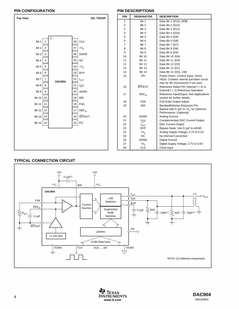
PIN DESIGNATOR DESCRIPTION
1 Bit 1 Data Bit 1 (D13), MSB2 Bit 2 Data Bit 2 (D12)3 Bit 3 Data Bit 3 (D11)4 Bit 4 Data Bit 4 (D10)5 Bit 5 Data Bit 5 (D9)6 Bit 6 Data Bit 6 (D8)7 Bit 7 Data Bit 7 (D7)8 Bit 8 Data Bit 8 (D6)9 Bit 9 Data Bit 9 (D5)10 Bit 10 Data Bit 10 (D4)11 Bit 11 Data Bit 11 (D3)12 Bit 12 Data Bit 12 (D2)13 Bit 13 Data Bit 13 (D1)14 Bit 14 Data Bit 14 (D0), LSB15 PD Power Down, Control Input; Active
HIGH. Contains internal pull-down circuit;may be left unconnected if not used.
16 INT/EXT Reference Select Pin; Internal ( = 0) orExternal ( = 1) Reference Operation
17 REFIN Reference Input/Ouput. See Applicationssection for further details.
18 FSA Full-Scale Output Adjust19 BW Bandwidth/Noise Reduction Pin:
Bypass with 0.1µF to +VA for OptimumPerformance. (Optional)
20 AGND Analog Ground21 IOUT Complementary DAC Current Output22 IOUT DAC Current Output23 BYP Bypass Node: Use 0.1µF to AGND24 +VA Analog Supply Voltage, 2.7V to 5.5V25 NC No Internal Connection26 DGND Digital Ground27 +VD Digital Supply Voltage, 2.7V to 5.5V28 CLK Clock Input
PIN DESCRIPTIONSPIN CONFIGURATION
Top View SO, TSSOP
TYPICAL CONNECTION CIRCUIT

DAC904 5SBAS095C www.ti.com
TIMING DIAGRAM
t2 t1
tS tH
tSETtPD
CLOCK
D13 D0
Iout orIout
Data ChangesStable Valid Data
Data Changes
SYMBOL DESCRIPTION MIN TYP MAX UNITS
t1 Clock Pulse HIGH Time 3 nst2 Clock Pulse LOW Time 3 nstS Data Setup Time 1.0 nstH Data Hold Time 1.5 nstPD Propagation Delay Time 1 nstSET Output Settling Time to 0.1% 30 ns
DAC9046SBAS095Cwww.ti.com
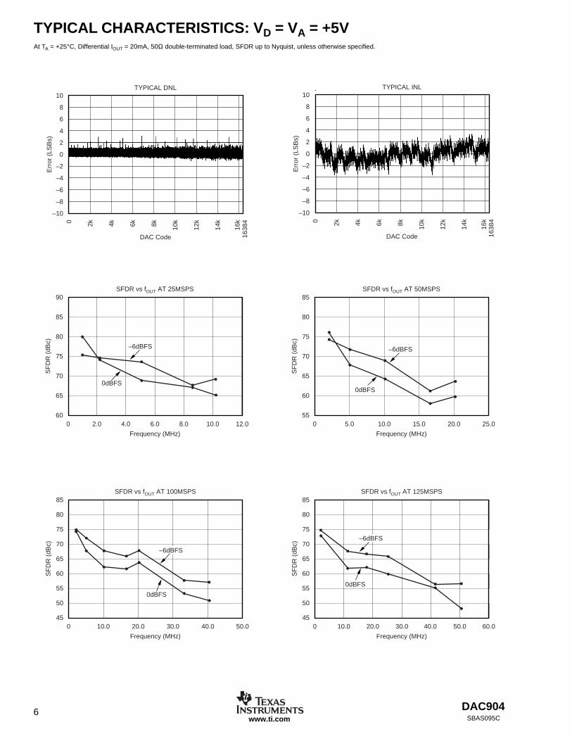
TYPICAL CHARACTERISTICS: VD = VA = +5VAt TA = +25°C, Differential IOUT = 20mA, 50Ω double-terminated load, SFDR up to Nyquist, unless otherwise specified.
DAC Code
TYPICAL DNL
Err
or (
LSB
s)
10
8
6
4
2
0
–2
–4
–6
–8
–10
0 2k 4k 6k 8k 10k
12k
14k
16k
1638
4
TYPICAL INL
Err
or (
LSB
s)
10
8
6
4
2
0
–2
–4
–6
–8
–10
DAC Code
0 2k 4k 6k 8k 10k
12k
14k
16k
1638
4
SFDR vs fOUT AT 25MSPS
Frequency (MHz)
SF
DR
(dB
c)
90
85
80
75
70
65
602.0 4.0 6.0 8.0 10.0 12.00
0dBFS
–6dBFS
SFDR vs fOUT AT 50MSPS
Frequency (MHz)
SF
DR
(dB
c)85
80
75
70
65
60
555.0 10.0 15.0 20.0 25.00
–6dBFS
0dBFS
SFDR vs fOUT AT 100MSPS
Frequency (MHz)
SF
DR
(dB
c)
85
80
75
70
65
60
55
50
4510.0 20.0 30.0 40.0 50.00
0dBFS
–6dBFS
SFDR vs fOUT AT 125MSPS
Frequency (MHz)
SF
DR
(dB
c)
85
80
75
70
65
60
55
50
4510.0 20.0 30.0 50.040.0 60.00
0dBFS
–6dBFS
DAC904 7SBAS095C www.ti.com
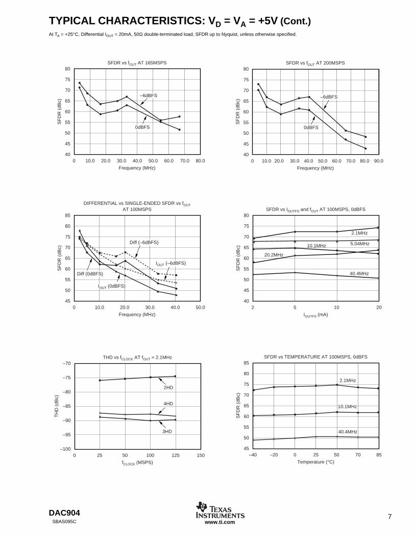
TYPICAL CHARACTERISTICS: VD = VA = +5V (Cont.)At TA = +25°C, Differential IOUT = 20mA, 50Ω double-terminated load, SFDR up to Nyquist, unless otherwise specified.
SFDR vs fOUT AT 165MSPS
Frequency (MHz)
SF
DR
(dB
c)
80
75
70
65
60
55
50
45
4020.010.0 30.0 40.0 50.0 70.060.0 80.00
–6dBFS
0dBFS
SFDR vs fOUT AT 200MSPS
Frequency (MHz)
SF
DR
(dB
c)
80
75
70
65
60
55
50
45
4020.010.0 30.0 40.0 50.0 70.060.0 90.080.00
–6dBFS
0dBFS
DIFFERENTIAL vs SINGLE-ENDED SFDR vs fOUTAT 100MSPS
Frequency (MHz)
SF
DR
(dB
c)
85
80
75
70
65
60
55
50
4510.0 20.0 30.0 40.0 50.00
Diff (0dBFS)
IOUT (–6dBFS)
IOUT (0dBFS)
Diff (–6dBFS)X
X
X
X
XX
X
SFDR vs IOUTFS and fOUT AT 100MSPS, 0dBFS
IOUTFS (mA)
SF
DR
(dB
c)
80
75
70
65
60
55
50
45
405 10 202
XX
XX
2.1MHz
20.2MHz
10.1MHz 5.04MHz
40.4MHz
*** *
THD vs fCLOCK AT fOUT = 2.1MHz
fCLOCK (MSPS)
TH
D (
dBc)
–70
–75
–80
–85
–90
–95
–10025 50 100 125 1500
2HD
4HD
3HD
X X XX
SFDR vs TEMPERATURE AT 100MSPS, 0dBFS
Temperature (°C)
SF
DR
(dB
c)
85
80
75
70
65
60
55
50
45–20 0 25 7050 85–40
2.1MHz
10.1MHz
40.4MHzXXXXXXX
DAC9048SBAS095Cwww.ti.com
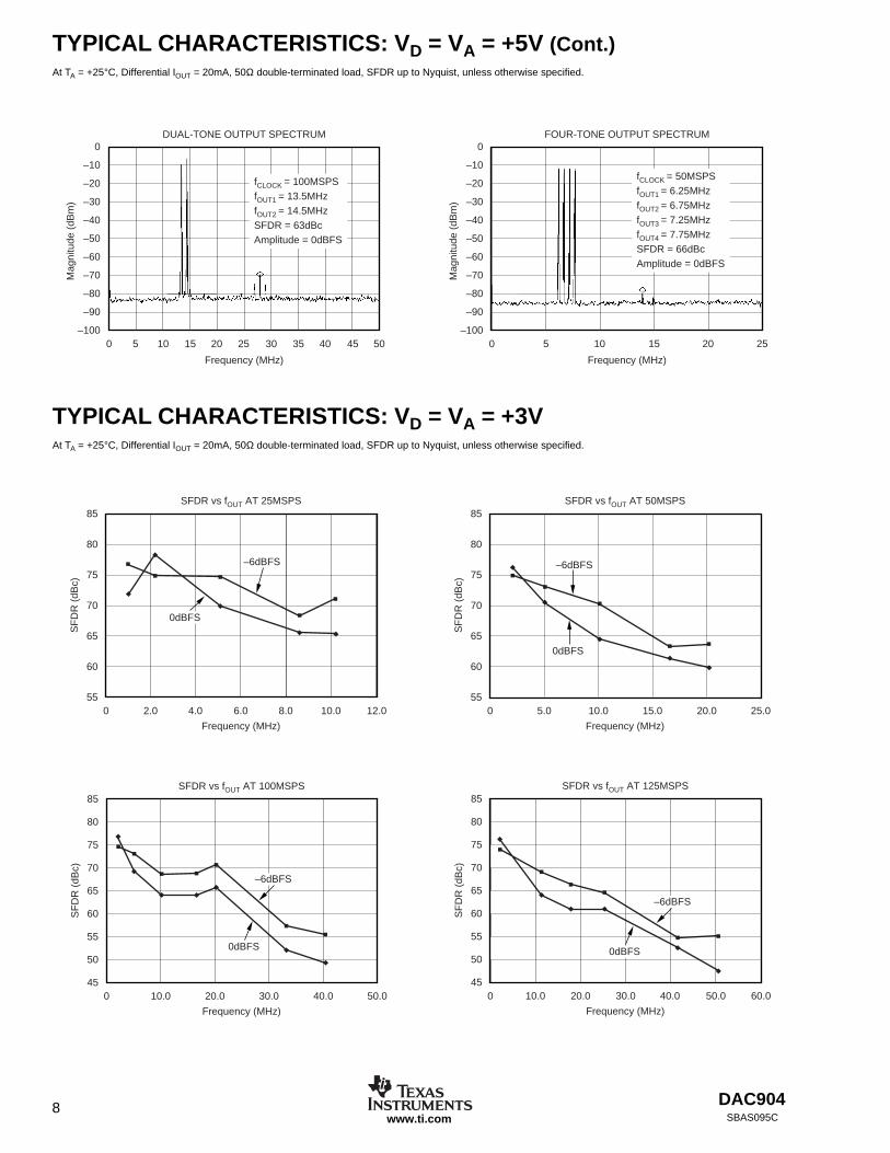
TYPICAL CHARACTERISTICS: VD = VA = +5V (Cont.)At TA = +25°C, Differential IOUT = 20mA, 50Ω double-terminated load, SFDR up to Nyquist, unless otherwise specified.
DUAL-TONE OUTPUT SPECTRUM
Frequency (MHz)
Mag
nitu
de (
dBm
)
0
0
–10
–20
–30
–40
–50
–60
–70
–80
–90
–1005 10 15 20 25 30 35 40 45 50
fCLOCK = 100MSPSfOUT1 = 13.5MHzfOUT2 = 14.5MHzSFDR = 63dBcAmplitude = 0dBFS
FOUR-TONE OUTPUT SPECTRUM
Frequency (MHz)
Mag
nitu
de (
dBm
)
0
0
–10
–20
–30
–40
–50
–60
–70
–80
–90
–1005 10 15 20 25
fCLOCK = 50MSPSfOUT1 = 6.25MHzfOUT2 = 6.75MHzfOUT3 = 7.25MHzfOUT4 = 7.75MHzSFDR = 66dBcAmplitude = 0dBFS
SFDR vs fOUT AT 25MSPS
Frequency (MHz)
SF
DR
(dB
c)
85
80
75
70
65
60
552.0 4.0 6.0 8.0 10.0 12.00
0dBFS
–6dBFS
SFDR vs fOUT AT 50MSPS
Frequency (MHz)
SF
DR
(dB
c)
85
80
75
70
65
60
555.0 10.0 15.0 20.0 25.00
–6dBFS
0dBFS
SFDR vs fOUT AT 100MSPS
Frequency (MHz)
SF
DR
(dB
c)
85
80
75
70
65
60
55
50
4510.0 20.0 30.0 40.0 50.00
–6dBFS
0dBFS
SFDR vs fOUT AT 125MSPS
Frequency (MHz)
SF
DR
(dB
c)
85
80
75
70
65
60
55
50
4510.0 20.0 30.0 50.040.0 60.00
0dBFS
–6dBFS
TYPICAL CHARACTERISTICS: VD = VA = +3VAt TA = +25°C, Differential IOUT = 20mA, 50Ω double-terminated load, SFDR up to Nyquist, unless otherwise specified.
DAC904 9SBAS095C www.ti.com
SFDR vs fOUT AT 165MSPS
Frequency (MHz)
SF
DR
(dB
c)
80
75
70
65
60
55
50
45
4020.010.0 30.0 40.0 50.0 70.060.0 80.00
–6dBFS
0dBFS
DIFFERENTIAL vs SINGLE-ENDED SFDR vs fOUTAT 100MSPS
Frequency (MHz)
SF
DR
(dB
c)
85
80
75
70
65
60
55
50
4510.0 20.0 30.0 40.0 50.00
Diff (0dBFS)
IOUT (–6dBFS)
IOUT (0dBFS)
Diff (–6dBFS)
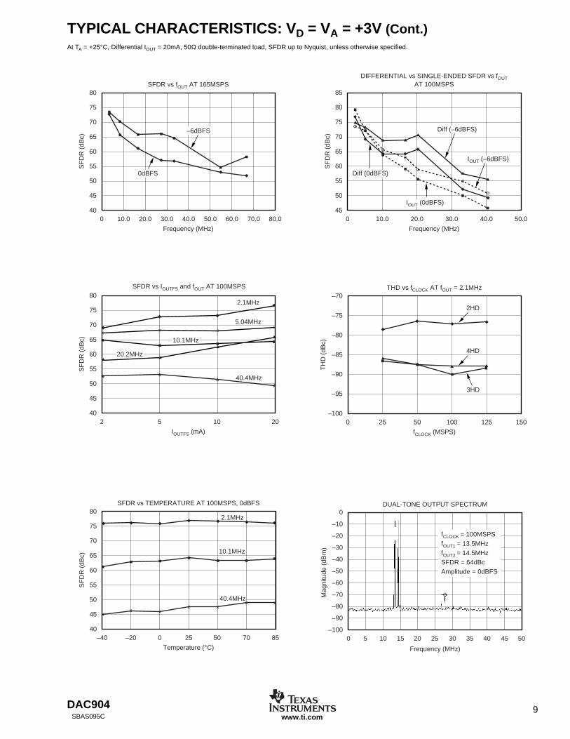
TYPICAL CHARACTERISTICS: VD = VA = +3V (Cont.)At TA = +25°C, Differential IOUT = 20mA, 50Ω double-terminated load, SFDR up to Nyquist, unless otherwise specified.
IOUTFS (mA)
SF
DR
(dB
c)
80
75
70
65
60
55
50
45
405 10 202
X X
*** *
X
X
SFDR vs IOUTFS and fOUT AT 100MSPS
2.1MHz
5.04MHz
20.2MHz
10.1MHz
40.4MHz
THD vs fCLOCK AT fOUT = 2.1MHz
fCLOCK (MSPS)
TH
D (
dBc)
–70
–75
–80
–85
–90
–95
–10025 50 100 125 1500
2HD
4HD
3HD
SFDR vs TEMPERATURE AT 100MSPS, 0dBFS
Temperature (°C)
SF
DR
(dB
c)
80
75
70
65
60
55
50
45
40–20 0 25 7050 85–40
2.1MHz
10.1MHz
40.4MHzXX
XXXX
X
DUAL-TONE OUTPUT SPECTRUM
Frequency (MHz)
Mag
nitu
de (
dBm
)
0
0
–10
–20
–30
–40
–50
–60
–70
–80
–90
–1005 10 15 20 25 30 35 40 45 50
fCLOCK = 100MSPSfOUT1 = 13.5MHzfOUT2 = 14.5MHzSFDR = 64dBcAmplitude = 0dBFS
DAC90410SBAS095Cwww.ti.com
APPLICATION INFORMATIONTHEORY OF OPERATION
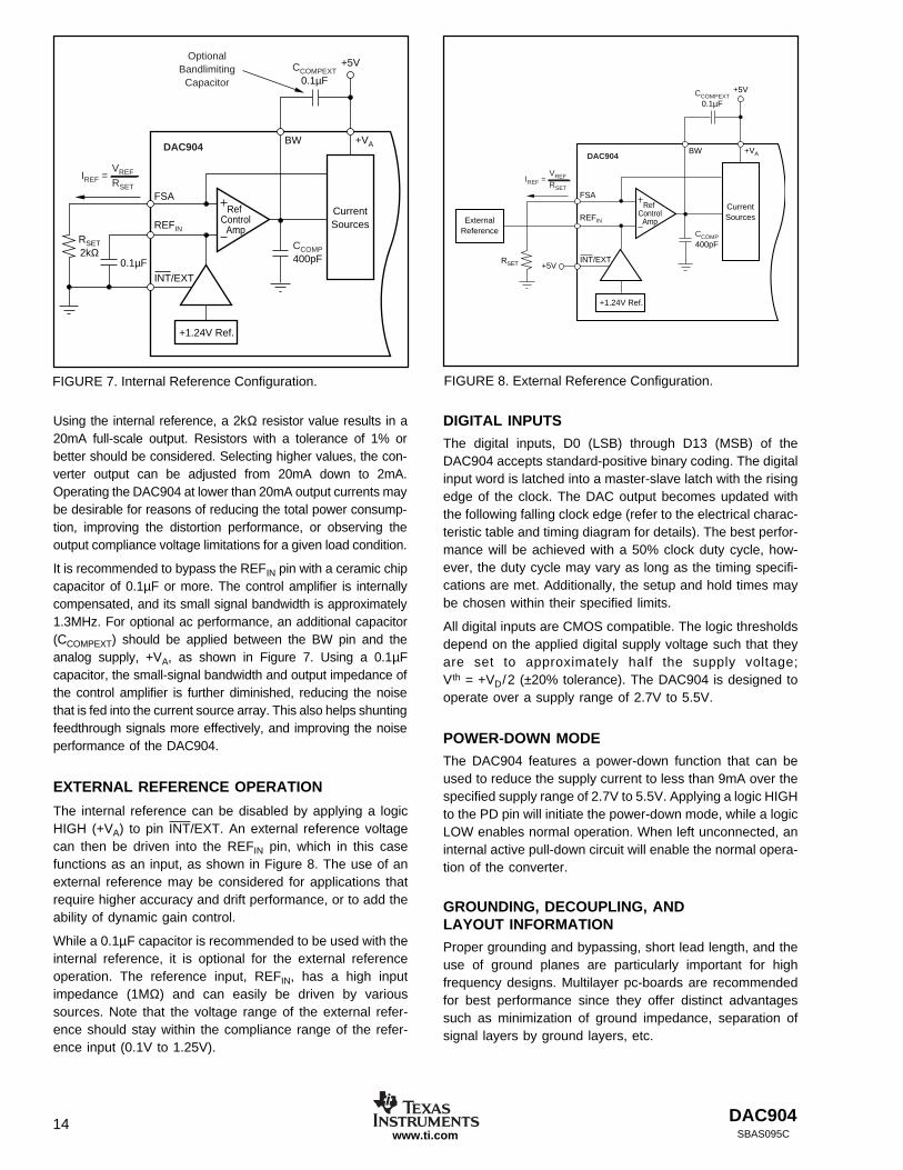
The architecture of the DAC904 uses the current steeringtechnique to enable fast switching and a high update rate. Thecore element within the monolithic DAC is an array of seg-mented current sources that are designed to deliver a full-scaleoutput current of up to 20mA, as shown in Figure 1. An internaldecoder addresses the differential current switches each timethe DAC is updated and a corresponding output current isformed by steering all currents to either output summing node,IOUT or IOUT. The complementary outputs deliver a differentialoutput signal that improves the dynamic performance throughreduction of even-order harmonics, common-mode signals(noise), and double the peak-to-peak output signal swing by afactor of two, compared to single-ended operation.
FIGURE 1. Functional Block Diagram of the DAC904.
PMOSCurrentSourceArray
LSBSwitches
SegmentedMSB
Switches
+1.24V Ref
Latches and SwitchDecoder Logic
14-Bit Data Input
D13...D0
DAC904
Full-ScaleAdjust
ResistorRef
ControlAmp
RefBuffer
BW +VD+VA
RSET2kΩ
CLK DGND
RefInput
0.1µF
INT/EXT
IOUT
IOUT
BYP
PD
20pF(1)50Ω
50Ω 20pF(1)
1:1VOUT
0.1µF
400pF
0.1µF(1)
+3V to +5VAnalog
BandwidthControl
+3V to +5VDigital
FSA
REFIN
AGND
AnalogGround
DigitalGround
Power Down(internal pull-down)
ClockInput
NOTE: Supply bypassing not shown. NOTE: (1) Optional.
TYPICAL CHARACTERISTICS: VD = VA = +3V (Cont.)At TA = +25°C, Differential IOUT = 20mA, 50Ω double-terminated load, SFDR up to Nyquist, unless otherwise specified.
FOUR-TONE OUTPUT SPECTRUM
Frequency (MHz)
Mag
nitu
de (
dBm
)
0
0
–10
–20
–30
–40
–50
–60
–70
–80
–90
–1005 10 15 20 25
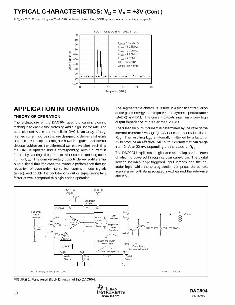
fCLOCK = 50MSPSfOUT1 = 6.25MHzfOUT2 = 6.75MHzfOUT3 = 7.25MHzfOUT4 = 7.75MHzSFDR = 67dBcAmplitude = 0dBFS
The segmented architecture results in a significant reductionof the glitch energy, and improves the dynamic performance(SFDR) and DNL. The current outputs maintain a very highoutput impedance of greater than 200kΩ.
The full-scale output current is determined by the ratio of theinternal reference voltage (1.24V) and an external resistor,RSET. The resulting IREF is internally multiplied by a factor of32 to produce an effective DAC output current that can rangefrom 2mA to 20mA, depending on the value of RSET.
The DAC904 is split into a digital and an analog portion, eachof which is powered through its own supply pin. The digitalsection includes edge-triggered input latches and the de-coder logic, while the analog section comprises the currentsource array with its associated switches and the referencecircuitry.

DAC904 11SBAS095C www.ti.com
DAC TRANSFER FUNCTION
The total output current, IOUTFS, of the DAC904 is the sum-mation of the two complementary output currents:
IOUTFS = IOUT + IOUT (1)
The individual output currents depend on the DAC code andcan be expressed as:
IOUT = IOUTFS • (Code/16384) (2)
IOUT = IOUTFS • (16383 – Code/16384) (3)
where ‘Code’ is the decimal representation of the DAC datainput word. Additionally, IOUTFS is a function of the referencecurrent IREF, which is determined by the reference voltageand the external setting resistor, RSET.
IOUTFS = 32 • IREF = 32 • VREF/RSET (4)
In most cases the complementary outputs will drive resistiveloads or a terminated transformer. A signal voltage willdevelop at each output according to:
VOUT = IOUT • RLOAD (5)
VOUT = IOUT • RLOAD (6)
The value of the load resistance is limited by the outputcompliance specification of the DAC904. To maintain speci-fied linearity performance, the voltage for IOUT and IOUT
should not exceed the maximum allowable compliance range.
The two single-ended output voltages can be combined tofind the total differential output swing:
(7)
V V VCode
I ROUTDIFF OUT OUT OUTFS LOAD= = • • •–( – )2 16383
16384
ANALOG OUTPUTS
The DAC904 provides two complementary current outputs,IOUT and IOUT. The simplified circuit of the analog outputstage representing the differential topology is shown inFigure 2. The output impedance of 200kΩ 12pF for IOUT
and IOUT results from the parallel combination of the differen-tial switches, along with the current sources and associatedparasitic capacitances.
The signal voltage swing that may develop at the twooutputs, IOUT and IOUT, is limited by a negative and positivecompliance. The negative limit of –1V is given by the break-down voltage of the CMOS process, and exceeding it willcompromise the reliability of the DAC904, or even causepermanent damage. With the full-scale output set to 20mA,the positive compliance equals 1.25V, operating with
FIGURE 2. Equivalent Analog Output.
IOUT IOUT
DAC904
RL RL
+VA
+VD = 5V. Note that the compliance range decreases toabout 1V for a selected output current of IOUTFS = 2mA.Care should be taken that the configuration of the DAC904does not exceed the compliance range to avoid degradationof the distortion performance and integral linearity.
Best distortion performance is typically achieved with themaximum full-scale output signal limited to approximately0.5V. This is the case for a 50Ω doubly-terminated load anda 20mA full-scale output current. A variety of loads can beadapted to the output of the DAC904 by selecting a suitabletransformer while maintaining optimum voltage levels atIOUT and IOUT. Furthermore, using the differential outputconfiguration in combination with a transformer will be instru-mental for achieving excellent distortion performance. Com-mon-mode errors, such as even-order harmonics or noise,can be substantially reduced. This is particularly the casewith high output frequencies and/or output amplitudes belowfull-scale.
For those applications requiring the optimum distortion andnoise performance, it is recommended to select a full-scaleoutput of 20mA. A lower full-scale range down to 2mA maybe considered for applications that require a low powerconsumption, but can tolerate a reduced performance level.
INPUT CODE (D13 - D0) IOUT IOUT
11 1111 1111 1111 20mA 0mA
10 0000 0000 0000 10mA 10mA
00 0000 0000 0000 0mA 20mA
TABLE I. Input Coding versus Analog Output Current.
OUTPUT CONFIGURATIONS
The current output of the DAC904 allows for a variety ofconfigurations, some of which are illustrated below. As men-tioned previously, utilizing the converter’s differential outputswill yield the best dynamic performance. Such a differentialoutput circuit may consist of an RF transformer (see Figure 3)or a differential amplifier configuration (see Figure 4). The

DAC90412SBAS095Cwww.ti.com
FIGURE 4. Difference Amplifier Provides Differential to Single-Ended Conversion and AC-Coupling.
The OPA680 is configured for a gain of 2. Therefore, oper-ating the DAC904 with a 20mA full-scale output will producea voltage output of ±1V. This requires the amplifier to operateoff of a dual power supply (±5V). The tolerance of theresistors typically sets the limit for the achievable common-mode rejection. An improvement can be obtained by finetuning resistor R4.
This configuration typically delivers a lower level of ac perfor-mance than the previously discussed transformer solutionbecause the amplifier introduces another source of distor-tion. Suitable amplifiers should be selected based on theirslew-rate, harmonic distortion, and output swing capabilities.High-speed amplifiers like the OPA680 or OPA687 may beconsidered. The ac performance of this circuit may beimproved by adding a small capacitor, CDIFF, between theoutputs IOUT and IOUT, as shown in Figure 4. This will introducea real pole to create a low-pass filter in order to slew-limit theDAC’s fast output signal steps that otherwise could drive theamplifier into slew-limitations or into an overload condition;both would cause excessive distortion. The difference ampli-fier can easily be modified to add a level shift for applicationsrequiring the single-ended output voltage to be unipolar, i.e.,swing between 0V and +2V.
IOUT
IOUT
DAC904
RL26.1Ω
RL28.7Ω
R4402Ω
R3200Ω
R2402Ω
R1200Ω
OPA680
CDIFF
+5V
VOUT
–5V
transformer configuration is ideal for most applications with accoupling, while op amps will be suitable for a DC-coupledconfiguration.
The single-ended configuration (see Figure 6) may be consid-ered for applications requiring a unipolar output voltage. Con-necting a resistor from either one of the outputs to ground willconvert the output current into a ground-referenced voltagesignal. To improve on the DC linearity, an I-to-V converter canbe used instead. This will result in a negative signal excursionand, therefore, requires a dual supply amplifier.
DIFFERENTIAL WITH TRANSFORMER
Using an RF transformer provides a convenient way ofconverting the differential output signal into a single-endedsignal while achieving excellent dynamic performance, asshown in Figure 3. The appropriate transformer should becarefully selected based on the output frequency spectrumand impedance requirements. The differential transformerconfiguration has the benefit of significantly reducing com-mon-mode signals, thus improving the dynamic performanceover a wide range of frequencies. Furthermore, by selectinga suitable impedance ratio (winding ratio), the transformercan be used to provide optimum impedance matching whilecontrolling the compliance voltage for the converter outputs.The model shown in Figure 3 has a 1:1 ratio and may beused to interface the DAC904 to a 50Ω load. This results ina 25Ω load for each of the outputs, IOUT and IOUT. The outputsignals are ac coupled and inherently isolated because of thetransformer's magnetic coupling.
As shown in Figure 3, the transformer’s center tap is con-nected to ground. This forces the voltage swing on IOUT andIOUT to be centered at 0V. In this case the two resistors, RS,may be replaced with one, RDIFF, or omitted altogether. Thisapproach should only be used if all components are close toeach other, and if the VSWR is not important. A completepower transfer from the DAC output to the load can berealized, but the output compliance range should be ob-served. Alternatively, if the center tap is not connected, thesignal swing will be centered at RS • IOUTFS/2. However, inthis case, the two resistors (RS) must be used to enable thenecessary DC-current flow for both outputs.
DIFFERENTIAL CONFIGURATION USING AN OP AMP
If the application requires a DC-coupled output, a differenceamplifier may be considered, as shown in Figure 4. Fourexternal resistors are needed to configure the voltage-feed-back op amp OPA680 as a difference amplifier performingthe differential to single-ended conversion. Under the shownconfiguration, the DAC904 generates a differential outputsignal of 0.5Vp-p at the load resistors, RL. The resistor valuesshown were selected to result in a symmetric 25Ω loading foreach of the current outputs since the input impedance of thedifference amplifier is in parallel to resistors RL, and shouldbe considered.
FIGURE 3. Differential Output Configuration Using an RFTransformer.
IOUT
IOUT
DAC904
1:1
ADT1-1WT(Mini-Circuits)
RS50Ω
RS50Ω
RLOptionalRDIFF

DAC904 13SBAS095C www.ti.com
FIGURE 5. Dual, Voltage-Feedback Amplifier OPA2680 FormsDifferential Transimpedance Amplifier.
DUAL TRANSIMPEDANCE OUTPUT CONFIGURATION
The circuit example of Figure 5 shows the signal outputcurrents connected into the summing junction of the OPA2680,which is set up as a transimpedance stage, or I-to-V con-verter. With this circuit, the DAC’s output will be kept at avirtual ground, minimizing the effects of output impedancevariations, and resulting in the best DC linearity (INL). How-ever, as mentioned previously, the amplifier may be driveninto slew-rate limitations, and produce unwanted distortion.This may occur especially at high DAC update rates.
The DC gain for this circuit is equal to feedback resistor RF.At high frequencies, the DAC output impedance (CD1, CD2)will produce a zero in the noise gain for the OPA2680 thatmay cause peaking in the closed-loop frequency response.CF is added across RF to compensate for this noise-gainpeaking. To achieve a flat transimpedance frequency re-sponse, the pole in each feedback network should be set to:
12 4π πR C
GBPR CF F F D
= (8)
with GBP = Gain Bandwidth Product of OPA,
which will give a corner frequency f-3dB of approximately:
fGBPR CdB
F D− =3 2π (9)
1/2OPA2680
1/2OPA2680
DAC904
–VOUT = IOUT • RF
–VOUT = IOUT • RF
RF1
RF2
CF1
CF2
CD1
CD2
IOUT
IOUT
50Ω
50Ω–5V
+5V
The full-scale output voltage is defined by the product ofIOUTFS • RF, and has a negative unipolar excursion. Toimprove on the ac performance of this circuit, adjustment ofRF and/or IOUTFS should be considered. Further extensions ofthis application example may include adding a differentialfilter at the OPA2680’s output followed by a transformer, inorder to convert to a single-ended signal.
SINGLE-ENDED CONFIGURATION
Using a single load resistor connected to the one of the DACoutputs, a simple current-to-voltage conversion can be ac-complished. The circuit in Figure 6 shows a 50Ω resistorconnected to IOUT, providing the termination of the furtherconnected 50Ω cable. Therefore, with a nominal outputcurrent of 20mA, the DAC produces a total signal swing of0V to 0.5V into the 25Ω load.
Different load resistor values may be selected as long as theoutput compliance range is not exceeded. Additionally, theoutput current, IOUTFS, and the load resistor may be mutuallyadjusted to provide the desired output signal swing andperformance.
FIGURE 6. Driving a Doubly-Terminated 50Ω Cable Directly.
IOUT
IOUT
DAC904
25Ω
50Ω 50Ω
IOUTFS = 20mAVOUT = 0V to +0.5V
INTERNAL REFERENCE OPERATION
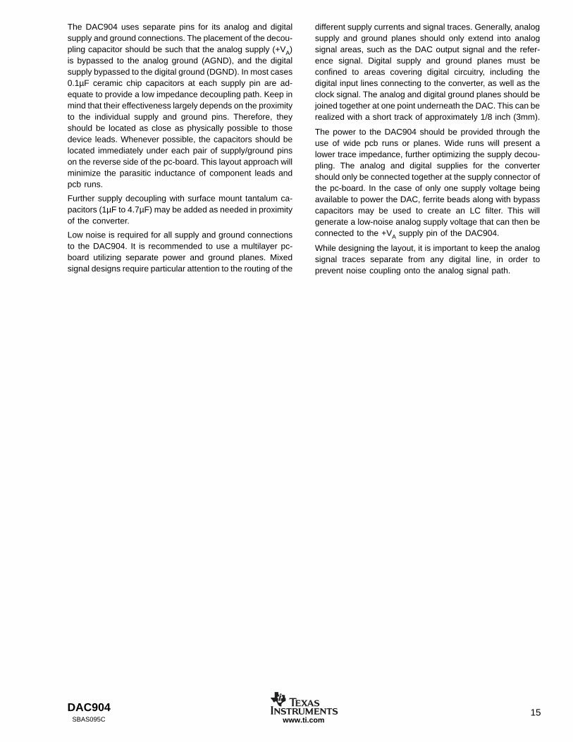
The DAC904 has an on-chip reference circuit that comprisesa 1.24V bandgap reference and a control amplifier. Ground-ing pin 16, INT/EXT, enables the internal reference opera-tion. The full-scale output current, IOUTFS, of the DAC904 isdetermined by the reference voltage, VREF, and the value ofresistor RSET. IOUTFS can be calculated by:
IOUTFS = 32 • IREF = 32 • VREF / RSET (10)
The external resistor RSET connects to the FSA pin (Full-Scale Adjust), see Figure 7. The reference control amplifieroperates as a V-to-I converter producing a reference current,IREF, which is determined by the ratio of VREF and RSET, asshown in Equation 10. The full-scale output current, IOUTFS,results from multiplying IREF by a fixed factor of 32.
DAC90414SBAS095Cwww.ti.com
FIGURE 8. External Reference Configuration.FIGURE 7. Internal Reference Configuration.
DIGITAL INPUTS
The digital inputs, D0 (LSB) through D13 (MSB) of theDAC904 accepts standard-positive binary coding. The digitalinput word is latched into a master-slave latch with the risingedge of the clock. The DAC output becomes updated withthe following falling clock edge (refer to the electrical charac-teristic table and timing diagram for details). The best perfor-mance will be achieved with a 50% clock duty cycle, how-ever, the duty cycle may vary as long as the timing specifi-cations are met. Additionally, the setup and hold times maybe chosen within their specified limits.
All digital inputs are CMOS compatible. The logic thresholdsdepend on the applied digital supply voltage such that theyare set to approximately half the supply voltage;Vth = +VD/2 (±20% tolerance). The DAC904 is designed tooperate over a supply range of 2.7V to 5.5V.
POWER-DOWN MODE
The DAC904 features a power-down function that can beused to reduce the supply current to less than 9mA over thespecified supply range of 2.7V to 5.5V. Applying a logic HIGHto the PD pin will initiate the power-down mode, while a logicLOW enables normal operation. When left unconnected, aninternal active pull-down circuit will enable the normal opera-tion of the converter.
GROUNDING, DECOUPLING, ANDLAYOUT INFORMATION
Proper grounding and bypassing, short lead length, and theuse of ground planes are particularly important for highfrequency designs. Multilayer pc-boards are recommendedfor best performance since they offer distinct advantagessuch as minimization of ground impedance, separation ofsignal layers by ground layers, etc.
Using the internal reference, a 2kΩ resistor value results in a20mA full-scale output. Resistors with a tolerance of 1% orbetter should be considered. Selecting higher values, the con-verter output can be adjusted from 20mA down to 2mA.Operating the DAC904 at lower than 20mA output currents maybe desirable for reasons of reducing the total power consump-tion, improving the distortion performance, or observing theoutput compliance voltage limitations for a given load condition.
It is recommended to bypass the REFIN pin with a ceramic chipcapacitor of 0.1µF or more. The control amplifier is internallycompensated, and its small signal bandwidth is approximately1.3MHz. For optional ac performance, an additional capacitor(CCOMPEXT) should be applied between the BW pin and theanalog supply, +VA, as shown in Figure 7. Using a 0.1µFcapacitor, the small-signal bandwidth and output impedance ofthe control amplifier is further diminished, reducing the noisethat is fed into the current source array. This also helps shuntingfeedthrough signals more effectively, and improving the noiseperformance of the DAC904.
EXTERNAL REFERENCE OPERATION
The internal reference can be disabled by applying a logicHIGH (+VA) to pin INT/EXT. An external reference voltagecan then be driven into the REFIN pin, which in this casefunctions as an input, as shown in Figure 8. The use of anexternal reference may be considered for applications thatrequire higher accuracy and drift performance, or to add theability of dynamic gain control.
While a 0.1µF capacitor is recommended to be used with theinternal reference, it is optional for the external referenceoperation. The reference input, REFIN, has a high inputimpedance (1MΩ) and can easily be driven by varioussources. Note that the voltage range of the external refer-ence should stay within the compliance range of the refer-ence input (0.1V to 1.25V).
DAC904
CCOMPEXT0.1µF
OptionalBandlimiting
Capacitor
CCOMP400pF
+1.24V Ref.
RSET2kΩ
0.1µF
INT/EXT
FSA
BW
+5V
+VA
REFIN
CurrentSources
IREF =VREF
RSET
Ref Control
Amp
RSET +5V
ExternalReference
IREF =VREF
RSET
DAC904
CCOMPEXT0.1µF
CCOMP400pF
+1.24V Ref.
INT/EXT
FSA
BW
+5V
+VA
REFIN
CurrentSources
Ref Control
Amp
DAC904 15SBAS095C www.ti.com
The DAC904 uses separate pins for its analog and digitalsupply and ground connections. The placement of the decou-pling capacitor should be such that the analog supply (+VA)is bypassed to the analog ground (AGND), and the digitalsupply bypassed to the digital ground (DGND). In most cases0.1µF ceramic chip capacitors at each supply pin are ad-equate to provide a low impedance decoupling path. Keep inmind that their effectiveness largely depends on the proximityto the individual supply and ground pins. Therefore, theyshould be located as close as physically possible to thosedevice leads. Whenever possible, the capacitors should belocated immediately under each pair of supply/ground pinson the reverse side of the pc-board. This layout approach willminimize the parasitic inductance of component leads andpcb runs.
Further supply decoupling with surface mount tantalum ca-pacitors (1µF to 4.7µF) may be added as needed in proximityof the converter.
Low noise is required for all supply and ground connectionsto the DAC904. It is recommended to use a multilayer pc-board utilizing separate power and ground planes. Mixedsignal designs require particular attention to the routing of the
different supply currents and signal traces. Generally, analogsupply and ground planes should only extend into analogsignal areas, such as the DAC output signal and the refer-ence signal. Digital supply and ground planes must beconfined to areas covering digital circuitry, including thedigital input lines connecting to the converter, as well as theclock signal. The analog and digital ground planes should bejoined together at one point underneath the DAC. This can berealized with a short track of approximately 1/8 inch (3mm).
The power to the DAC904 should be provided through theuse of wide pcb runs or planes. Wide runs will present alower trace impedance, further optimizing the supply decou-pling. The analog and digital supplies for the convertershould only be connected together at the supply connector ofthe pc-board. In the case of only one supply voltage beingavailable to power the DAC, ferrite beads along with bypasscapacitors may be used to create an LC filter. This willgenerate a low-noise analog supply voltage that can then beconnected to the +VA supply pin of the DAC904.
While designing the layout, it is important to keep the analogsignal traces separate from any digital line, in order toprevent noise coupling onto the analog signal path.

PACKAGE OPTION ADDENDUM
www.ti.com 26-Oct-2016
Addendum-Page 1
PACKAGING INFORMATION
Orderable Device Status(1)
Package Type PackageDrawing
Pins PackageQty
Eco Plan(2)
Lead/Ball Finish(6)
MSL Peak Temp(3)
Op Temp (°C) Device Marking(4/5)
Samples
DAC904E ACTIVE TSSOP PW 28 50 Green (RoHS& no Sb/Br)
CU NIPDAU Level-2-260C-1 YEAR -40 to 85 DAC904E
DAC904E/2K5 ACTIVE TSSOP PW 28 2500 Green (RoHS& no Sb/Br)
CU NIPDAU Level-2-260C-1 YEAR -40 to 85 DAC904E
DAC904U ACTIVE SOIC DW 28 20 Green (RoHS& no Sb/Br)
CU NIPDAU Level-2-260C-1 YEAR -40 to 85 DAC904U
DAC904U/1K ACTIVE SOIC DW 28 1000 Green (RoHS& no Sb/Br)
CU NIPDAU Level-2-260C-1 YEAR -40 to 85 DAC904U
(1) The marketing status values are defined as follows:ACTIVE: Product device recommended for new designs.LIFEBUY: TI has announced that the device will be discontinued, and a lifetime-buy period is in effect.NRND: Not recommended for new designs. Device is in production to support existing customers, but TI does not recommend using this part in a new design.PREVIEW: Device has been announced but is not in production. Samples may or may not be available.OBSOLETE: TI has discontinued the production of the device.
(2) Eco Plan - The planned eco-friendly classification: Pb-Free (RoHS), Pb-Free (RoHS Exempt), or Green (RoHS & no Sb/Br) - please check http://www.ti.com/productcontent for the latest availabilityinformation and additional product content details.TBD: The Pb-Free/Green conversion plan has not been defined.Pb-Free (RoHS): TI's terms "Lead-Free" or "Pb-Free" mean semiconductor products that are compatible with the current RoHS requirements for all 6 substances, including the requirement thatlead not exceed 0.1% by weight in homogeneous materials. Where designed to be soldered at high temperatures, TI Pb-Free products are suitable for use in specified lead-free processes.Pb-Free (RoHS Exempt): This component has a RoHS exemption for either 1) lead-based flip-chip solder bumps used between the die and package, or 2) lead-based die adhesive used betweenthe die and leadframe. The component is otherwise considered Pb-Free (RoHS compatible) as defined above.Green (RoHS & no Sb/Br): TI defines "Green" to mean Pb-Free (RoHS compatible), and free of Bromine (Br) and Antimony (Sb) based flame retardants (Br or Sb do not exceed 0.1% by weightin homogeneous material)
(3) MSL, Peak Temp. - The Moisture Sensitivity Level rating according to the JEDEC industry standard classifications, and peak solder temperature.
(4) There may be additional marking, which relates to the logo, the lot trace code information, or the environmental category on the device.
(5) Multiple Device Markings will be inside parentheses. Only one Device Marking contained in parentheses and separated by a "~" will appear on a device. If a line is indented then it is a continuationof the previous line and the two combined represent the entire Device Marking for that device.
(6) Lead/Ball Finish - Orderable Devices may have multiple material finish options. Finish options are separated by a vertical ruled line. Lead/Ball Finish values may wrap to two lines if the finishvalue exceeds the maximum column width.

PACKAGE OPTION ADDENDUM
www.ti.com 26-Oct-2016
Addendum-Page 2
Important Information and Disclaimer:The information provided on this page represents TI's knowledge and belief as of the date that it is provided. TI bases its knowledge and belief on informationprovided by third parties, and makes no representation or warranty as to the accuracy of such information. Efforts are underway to better integrate information from third parties. TI has taken andcontinues to take reasonable steps to provide representative and accurate information but may not have conducted destructive testing or chemical analysis on incoming materials and chemicals.TI and TI suppliers consider certain information to be proprietary, and thus CAS numbers and other limited information may not be available for release.
In no event shall TI's liability arising out of such information exceed the total purchase price of the TI part(s) at issue in this document sold by TI to Customer on an annual basis.

TAPE AND REEL INFORMATION
*All dimensions are nominal
Device PackageType
PackageDrawing
Pins SPQ ReelDiameter
(mm)
ReelWidth
W1 (mm)
A0(mm)
B0(mm)
K0(mm)
P1(mm)
W(mm)
Pin1Quadrant
DAC904E/2K5 TSSOP PW 28 2500 330.0 16.4 6.9 10.2 1.8 12.0 16.0 Q1
DAC904U/1K SOIC DW 28 1000 330.0 32.4 11.35 18.67 3.1 16.0 32.0 Q1
PACKAGE MATERIALS INFORMATION
www.ti.com 28-Oct-2012
Pack Materials-Page 1

*All dimensions are nominal
Device Package Type Package Drawing Pins SPQ Length (mm) Width (mm) Height (mm)
DAC904E/2K5 TSSOP PW 28 2500 367.0 367.0 38.0
DAC904U/1K SOIC DW 28 1000 367.0 367.0 55.0
PACKAGE MATERIALS INFORMATION
www.ti.com 28-Oct-2012
Pack Materials-Page 2


IMPORTANT NOTICE
Texas Instruments Incorporated and its subsidiaries (TI) reserve the right to make corrections, enhancements, improvements and otherchanges to its semiconductor products and services per JESD46, latest issue, and to discontinue any product or service per JESD48, latestissue. Buyers should obtain the latest relevant information before placing orders and should verify that such information is current andcomplete. All semiconductor products (also referred to herein as “components”) are sold subject to TI’s terms and conditions of salesupplied at the time of order acknowledgment.TI warrants performance of its components to the specifications applicable at the time of sale, in accordance with the warranty in TI’s termsand conditions of sale of semiconductor products. Testing and other quality control techniques are used to the extent TI deems necessaryto support this warranty. Except where mandated by applicable law, testing of all parameters of each component is not necessarilyperformed.TI assumes no liability for applications assistance or the design of Buyers’ products. Buyers are responsible for their products andapplications using TI components. To minimize the risks associated with Buyers’ products and applications, Buyers should provideadequate design and operating safeguards.TI does not warrant or represent that any license, either express or implied, is granted under any patent right, copyright, mask work right, orother intellectual property right relating to any combination, machine, or process in which TI components or services are used. Informationpublished by TI regarding third-party products or services does not constitute a license to use such products or services or a warranty orendorsement thereof. Use of such information may require a license from a third party under the patents or other intellectual property of thethird party, or a license from TI under the patents or other intellectual property of TI.Reproduction of significant portions of TI information in TI data books or data sheets is permissible only if reproduction is without alterationand is accompanied by all associated warranties, conditions, limitations, and notices. TI is not responsible or liable for such altereddocumentation. Information of third parties may be subject to additional restrictions.Resale of TI components or services with statements different from or beyond the parameters stated by TI for that component or servicevoids all express and any implied warranties for the associated TI component or service and is an unfair and deceptive business practice.TI is not responsible or liable for any such statements.Buyer acknowledges and agrees that it is solely responsible for compliance with all legal, regulatory and safety-related requirementsconcerning its products, and any use of TI components in its applications, notwithstanding any applications-related information or supportthat may be provided by TI. Buyer represents and agrees that it has all the necessary expertise to create and implement safeguards whichanticipate dangerous consequences of failures, monitor failures and their consequences, lessen the likelihood of failures that might causeharm and take appropriate remedial actions. Buyer will fully indemnify TI and its representatives against any damages arising out of the useof any TI components in safety-critical applications.In some cases, TI components may be promoted specifically to facilitate safety-related applications. With such components, TI’s goal is tohelp enable customers to design and create their own end-product solutions that meet applicable functional safety standards andrequirements. Nonetheless, such components are subject to these terms.No TI components are authorized for use in FDA Class III (or similar life-critical medical equipment) unless authorized officers of the partieshave executed a special agreement specifically governing such use.Only those TI components which TI has specifically designated as military grade or “enhanced plastic” are designed and intended for use inmilitary/aerospace applications or environments. Buyer acknowledges and agrees that any military or aerospace use of TI componentswhich have not been so designated is solely at the Buyer's risk, and that Buyer is solely responsible for compliance with all legal andregulatory requirements in connection with such use.TI has specifically designated certain components as meeting ISO/TS16949 requirements, mainly for automotive use. In any case of use ofnon-designated products, TI will not be responsible for any failure to meet ISO/TS16949.
Products ApplicationsAudio www.ti.com/audio Automotive and Transportation www.ti.com/automotiveAmplifiers amplifier.ti.com Communications and Telecom www.ti.com/communicationsData Converters dataconverter.ti.com Computers and Peripherals www.ti.com/computersDLP® Products www.dlp.com Consumer Electronics www.ti.com/consumer-appsDSP dsp.ti.com Energy and Lighting www.ti.com/energyClocks and Timers www.ti.com/clocks Industrial www.ti.com/industrialInterface interface.ti.com Medical www.ti.com/medicalLogic logic.ti.com Security www.ti.com/securityPower Mgmt power.ti.com Space, Avionics and Defense www.ti.com/space-avionics-defenseMicrocontrollers microcontroller.ti.com Video and Imaging www.ti.com/videoRFID www.ti-rfid.comOMAP Applications Processors www.ti.com/omap TI E2E Community e2e.ti.comWireless Connectivity www.ti.com/wirelessconnectivity
Mailing Address: Texas Instruments, Post Office Box 655303, Dallas, Texas 75265Copyright © 2016, Texas Instruments Incorporated