Saved from: · Computer Architecture and Microprocessor Ass.Prof.Shaimaa ... on.datapath The...
99
Saved from: www.uotechnology.edu.iq/dep-cs
Transcript of Saved from: · Computer Architecture and Microprocessor Ass.Prof.Shaimaa ... on.datapath The...

Saved from wwwuotechnologyeduiqdep-cs
Computer Architecture and
Microprocessor
AssProfShaimaa Hameed Shaker
References 1 fundamentals of computer organization and architecture by
Mostafa Abd-El-Barr Hesham El-Rewini 1PstP edition2005
2 David A Patterson and John L Hennessy Computer
Organization and Design1998
3 M M Mano computer system architecture third edition
prentice Hall 1993
4 Walter A Triebel The 80386 80486 and Pentiumreg Processors
HardwareSoftware and Interfaceing 1998
Introduction
The performance of a program depends on a combination of the
effectiveness of the algorithms used in the program the software systems
used to create and translate the program into machine instructions and
the effectiveness of the computer in executing those instructions which
may include inputoutput (IO) operations
If we open the box containing the computer we see a fascinating board of
thin plastic covered with dozens of small gray or black rectangles
Figure 17 shows the contents of the laptop computer in Figure 15
The motherboard is shown in the upper part of the photo Two disk drives
are in frontmdashthe hard drive on the left and a DVD drive on the right The
hole in the middle is for the laptop battery The small rectangles on the
motherboard contain the devices that drive our advancing technology
called integrated circuits and nicknamed chips
The board is composed of three pieces the piece connecting to the IO
devices mentioned earlier the memory and the processor The memory is
where the programs are kept when they are running it also contains the
data needed by the running programs Figure 18 shows that memory is
found on the two small boards and each small memory board contains
eight integrated circuits
The memory in Figure 18 is built from DRAM chips
DRAM stands for dynamic random access memory Several DRAMs are
used together to contain the instructions and data of a program In
contrast to sequential access memories such as magnetic tapes the RAM
portion of the term DRAM means that memory accesses take basically
the same amount of time no matter what portion of the memory is read
motherboard A plastic board containing packages of integrated circuits or chips
including processor cache memory and connectors for IO devices
such as networks and disks integrated circuit Also called a chip A
device combining dozens to millions of transistorsmemory The storage
area in which programs are kept when they are running and that
contains the data needed by the running programs
dynamic random access memory (DRAM) Memory built as an integrated circuit it provides
random access to any location
The processor is the active part of the board following the instructions of
a program to the letter It adds numbers tests numbers signals IO
devices to activate and so on The processor is under the fan and covered
by a heat sink on the left side of Figure 17 Occasionally people call the
processor the CPU for the more bureaucratic-sounding central processor
unit Descending even lower into the hardware Figure 19 reveals details
of a microprocessor The processor logically comprises two main
components datapath and control the respective brawn and brain of the
processor The datapath performs the arithmetic operations and control
tells the datapath memory and IO devices what to do according to the
wishes of the instructions of the program
central processor
unit (CPU) Also called processor The active part of the computer
which contains the datapath and control and which adds
numbers tests numberssignals IO devices toactivate and so
ondatapath The component of the processor that performs arithmetic
operationscontrol The component of the processor that commands the
datapath memory and IO devices
One of the most important abstractions is the interface between the
hardware and the lowest-level software abstraction A model that renders
lower-level details of computer systems temporarily invisible to facilitate
design of sophisticated systems
name the instruction set architecture or simply architecture of a
computer The instruction set architecture includes anything programmers
need to know to make a binary machine language program work
correctly including instructions IO devices and so on Typically the
operating system will encapsulate the details of doing IO allocating
memory and other low-level system functions so that application
programmers do not need to worry about such details The combination
of the basic instruction set and the operating system interface provided
for application programmers is called the application binary interface
(ABI)
instruction set architecture Also called architecture An abstract interface between
the hardware and the lowest-level software that encompasses all the information
necessary to write a machine languageprogram that will runcorrectly including
instructions registers memory access IO
An instruction set architecture allows computer designers to talk about
functions independently from the hardware that performs them For
example we can talk about the functions of a digital clock (keeping time
displaying the time setting the alarm) independently from the clock
hardware (quartz crystal LED displays plastic buttons) Computer
implementation of an architecture along the same lines
an implementation is hardware that obeys the architecture abstracti on
Both hardware and software consist of hierarchical layers with each
lower layer hiding details from the level above This principle of
abstraction is the way both hardware designers and software
designers cope with the complexity of computer systems One key
interface between the levels of abstraction is the instruction set
architecturemdashthe interface between the hardware and low-level
software This abstract interface enables many implementations of
varying cost and performance to run identical software
Technologies for Processors Processors and memory have improved at an incredible rate because
computer designers have long embraced the latest in electronic
technology to try to win the race to design a better computer Figure 111
shows the technologies that have been used over time
Performance
we need to determine the time taken by a computer to execute a given
job We define the clock cycle time as the time between two consecutive
rising (trailing) edges of a periodic clock signal (Fig 11)
Clock cycles allow counting unit computations because the storage of
computation results is synchronized with rising (trailing) clock edges
The time required to execute a job by a computer is often expressed in
terms of clock cycles We denote the number of CPU clock cycles for
executing a job to be the cycle count (CC) the cycle time by CT and the
clock frequency by f =1CT The time taken by the CPU to execute a job
can be expressed as
CPU time = CC X CT = CCf
It may be easier to count the number of instructions executed in a given
program as compared to counting the number of CPU clock cycles
needed for executing that program
Defining Performance we can define computer performance in several different ways
If you were running a program on two different desktop computers youd
say that the faster one is the desktop computer that gets the job done first
If you were running a datacenter that had several servers running jobs
submitted by many users youd say that the faster computer was the one
that completed the most jobs during a day
As an individual computer user you are interested in reducing response
timemdashthe time between the start and completion of a taskmdashalso referred
to as execution time Data center managers are often interested in
increasing throughput or bandwidthmdashthe total amount of work done in a
given time Hence in most cases we will need different performance
metrics as well as different sets of applications to benchmark embedded
and desktop computers which are more focused on response time versus
servers which are more focused on throughput
Therefore the average number of clock cycles per instruction (CPI) has
been used as an alternate performance measure The following equation
shows how to compute the CPI
CPI =CPU clock cycles for the programInstruction count
CPU time = Instruction count X CPI X Clock cycle time
= (Instruction count X CPI)Clock rate
It is known that the instruction set of a given machine consists of a
number of instruction categories ALU (simple assignment and arithmetic
and logic instructions) load store branch and so on In the case that the
CPI for each instruction category is known the overall CPI can be
computed as
CPI= sum 119862119875119868119894 119883 Ii119899
119894=1Instruction count
where Ii is the number of times an instruction of type i is executed in the
program and CPIi is the average number of clock cycles needed to
execute such instruction
Example Consider computing the overall CPI for a machine A for
which the following performance measures were recorded when
executing a set of benchmark programs Assume that the clock rate of the
CPU is 200 MHz
It should be noted that the CPI reflects the organization and the
instruction set architecture of the processor while the instruction count
reflects the instruction set architecture and compiler technology used
This shows the degree of interdependence between the two performance
parameters Therefore it is imperative that both the CPI and the
instruction count are considered in assessing the merits of a given
computer or equivalently in comparing the performance of two machines
A different performance measure that has been given a lot of attention in
recent years is MIPS (million instructions-per-second (the rate of
instruction execution per unit time)) which is defined as
Microprocessor
1-Microprocessor 8086 The brain or engine of the PC is the processor
(sometimes called microprocessor) or central processing unit (CPU)
The CPU performs the systemrsquos calculating and processing
The processor is easily the most expensive single component in the
system costing up to four or more times greater than the motherboard it
plugs into
2- Microprocessor Architecture A computer system has three main
components a Central Processing Unit (CPU) or processor a Memory
Unit and Input Output Units (devices) In any microcomputer system the
component which actually processes data is entirely contained on a single
chip called Microprocessor (MPU) This MPU can be programmed using
assembly language Writing a program in assembly language requires a
knowledge of the computer hardware (or Architecture) and the details of
its instruction set
The main internal hardware features of a computer are the processor
memory and registers (registers are special processor components for
holding address and data) The external hardware features are the
computer Input Output devices such as keyboard monitor
Software consists of the operating system (OS) and various programs
and data files stored on disk
Inside any computer based on a member of the 8086 family the basic
arrangement of the main components is shown in Figure 1
Information is sent from one main component to another along the
communication channel which is often called the System Bus Both
programs and data are stored in the memory The Bus Interface Unit
(BIU) within the MPU fetches new instruction or data as necessary It is
also the BIU jobs to interpret or decode instruction and to route results
to their proper destination
The MPU Execution Unit carries out any arithmetic which is required
including memory calculation Microcomputer memories consist of a
collection of chips of two kinds Read Only Memory (ROM) and Random
Access Memories (RAM)
3 Features of 8086 Microprocessor
1 Intel 8086 was launched in 1978
2 It was the first 16-bit microprocessor
3 This microprocessor had major improvement over the execution speed
of 8085
4 It is available as 40-pin Dual-Inline-Package (DIP)
5 It is available in three versions
a 8086 (5 MHz)
b 8086-2 (8 MHz)
c 8086-1 (10 MHz)
6 It consists of 29000 transistors
4 System Bus The components of the computer system must
communicate with each other and with the outside world Although it
may be possible to connect each component to the CPU separately as a
practical matter this would require too many physical connects To keep
the number of connections manageable the processor is connected to
memory and all peripherals using a bus
A Bus is a bunch of wires and electrical path on the printed IC to which
everything in the system is connected There are three types of Bus
1- Address Buss (AB) the width of AB determines the amount of
physical memory addressable by the processor
2- Data Bus (DB) the width of DB indicates the size of the data
transferred between the processor and memory or IO device
3- Control Bus (CB) consists of a set of control signals typical control
signals includes memory read memory write IO read IO write
interrupt acknowledge bus request These control signals indicates the
type of action taking place on the system bus
5- The Process Intel 8086
The 8086 CPU is divided into two independent functional units
1- Bus Interface Unit (BIU)
2- Execution Unit (EU)
Bus Interface Unit (BIU)
The function of BIU is to
bullFetch the instruction or data from memory
bullWrite the data to memory
bullWrite the data to the port
bullRead data from the port
Instruction Queue
1- To increase the execution speed BIU fetches as many as six
instruction bytes ahead to time from memory
2 All six bytes are then held in first in first out 6 byte register called
instruction queue
3 Then all bytes have to be given to EU one by one
4 This pre fetching operation of BIU may be in parallel with execution
operation of EU which improves the speed execution of the instruction
Execution Unit (EU)
The functions of execution unit are
bullTo tell BIU where to fetch the instructions or data from
bullTo decode the instructions
bullTo execute the instructions
The EU contains the control circuitry to perform various internal
operations A decoder in EU decodes the instruction fetched memory to
generate different internal or external control signals required to perform
the operation EU has 16- bit ALU which can perform arithmetic and
logical operations on 8-bit as well as 16-bit
These operation as shown in Figure 2
Example of Fetch and Execute process To execute the following instruction and store the result in memory
3+5=
Given PC=200 assume load rarr4
Addrarr5
Storerarr6 1-
a-load 500 to AC
b-Add 501
c-Store 502
500rarr3
501rarr5
502 empty till find result and store
2-
Pc=200
200 4 500
201
202
200 PC
AC
IR
The result of first instruction
3-Now The second instruction
Add 501
200 4 500
201 5 501
202 6 502
200 PC
AC
4 500 IR
The third instruction
Fetch processing is end to take all information to cpu
500 3
501 5
502
500 3
501 5
502
4- Now execute process is begin
200 4 500
201 5 501
202 6 502
201 PC
3 AC
4 500 IR
5-Now make fetch again as the following
200 4 500
201 5 501
202 6 502
201 PC
3 AC
5 501 IR
6- Now The execute stage
200 4 500
201 5 501
202 6 502
500 3
501 5
502
500 3
501 5
502
Get 501 and adding with AC
Now the result of AC=8
7- Now the fetch stage
200 4 500
201 5 501
202 6 502
IR take the instruction from RAM and get it to CPU by fetching
process to begin with execution process ie store the content of AC in 502
8- Now execution stage
PC increment ie PC=203
200 4 500
201 5 501
202 6 502
500 3
501 5
502
202 PC
3 AC
5 501 IR
202 PC
3+5=8 AC
5 501 IR
500 3
501 5
502
202 PC
8 AC
6 502 IR
6- Memory The memory of a computer system consist of tiny electronic switches
with each switch set in one of two states open or close It is however
more convenient to think of these states as 0 and 1 Thus each switch can
represent a binary digit or bit as it is known the memory unit consists of
millions of such bits bits are organized into groups of eight bits called
byte Memory can be viewed as consisting of an ordered sequence of
bytes Each byte in this memory can be identified by its sequence number
starting with 0 is shown in Figure 3 This is referred to as memory
address of the byte Such memory is called byte addressable memory
8086 can address up to 1 MB (220 bytes) of main memory this magic
number comes from the fact that the address bud of the 8086 has 20
500 3
501 5
502 8
203 PC
8 AC
6 502 IR
address lines This number is referred to as the Memory Address Space
(MAS) The memory address space of a system is determined by the
address bus width of the CPU used in the system The actual memory in a
system is always less than or equal to the MAS
Two basic memory operations
The memory unit supports two fundamental operations Read and Write
The read operation read a previously stored data and the write operation
stores a value in memory is shown in Figure 4
Steps in a typical read cycle
1- Place the address of the location to be read on the address bus
2- Activate the memory read control signal on the control bus
3- Wait for the memory to retrieve the data from the address memory
location
4- Read the data from the data bus
5- Drop the memory read control signal to terminate the read cycle
Steps in a typical write cycle
1- Place the address of the location to be written on the address bus
2- Place the data to be written on the data bus
3- Activate the memory write control signal on the control bus
4- Wait for the memory to store the data at the address location
5- Drop the memory write control signal to terminate the write cycle
Addresses group of bits which are arranged sequentially in memory to
enable direct access a number called address is associated with each
group Addresses start at 0 and increase for successive groups The term
location refers to a group of bits with a unique address
addressess type
1 Logical address=CSIP
2 Offset address= CS0+IP
3 Physical address= CS0+offset address
4 Lower range= CS+0000 or 00000
5 Upper rang= CS+FFFF
Example
If CS=24F6H and IP 634AH
The Logical address= CSIP then 24F6634A
Offset address= CS0+IP then 634A
Physical address= CS0+offset address then
2B2AA(24F60+634A)
Lower range= CS+0000 then 24F60(24F60+0000)
Upper rang= CS+FFFF then 34F5F(24F60+FFFF)
7- INPUTOUTPUT
Input Output (IO) devices provide the means by which the computer
system can interact with the outside world Computers use IO devices
(also called peripheral devices) for two major purposes
1- To communicate with the outside world and
2- Store data
Devices that are used to communicate like printer keyboard modem
Devices that are used to store data like disk drive IO devices are
connected to the system bus through IO controller (interface) ndash which
acts as interface between the system bus and IO devices
There are two main reasons for using IO controllers
1- IO devices exhibit different characteristics and if these devices are
connected directly the CPU would have to understand and respond
appropriately to each IO device This would cause the CPU to spend a lot
of time interacting with IO devices and spend less time executing user
programs
2- The amount of electrical power used to send signals on the system bus
is very low This means that the cable connecting the IO device has to be
very short (a few centimeters at most) IO controllers typically contain
driver hardware to send current over long cable that connects IO devices
is shown in Figure5
General Purpose Registers of 8086
1- General Purpose Registers of 8086
These registers can be used as 8-bit registers individually or can be used
as 16-bit in pair to have AX BX CX and DX
1 AX Register AX register is also known as accumulator register that
stores operands for arithmetic operation like divided rotate
2 BX Register This register is mainly used as a base register It holds the
starting base location of a memory region within a data segment
3 CX Register It is defined as a counter It is primarily used in loop
instruction to store loop counter
4 DX Register DX register is used to contain IO port address for IO
instruction
Example of important registers
AX=16bit
ALAH=8bit
MOV AXBX radic
MOV ALBL radic
MOV AHBH radic
MOV ALBH radic
MOV ALBX times
2- Segment Registers
Additional registers called segment registers generate memory address
when combined with other in the microprocessor In 8086
microprocessor memory is divided into 4 segments as shown in figure
below
1 Code Segment (CS) The CS register is used for addressing a memory
location in the Code Segment of the memory where the executable
program is stored
2 Data Segment (DS) The DS contains most data used by program
Data are accessed in the Data Segment by an offset address or the content
of other register that holds the offset address
3 Stack Segment (SS) SS defined the area of memory used for the
stack
4 Extra Segment (ES) ES is additional data segment that is used by
some of the string to hold the destination data
3- Flag Registers of 8086
Flag register in EU is of 16-bit
Flags Register determines the current state of the processor They are
modified automatically by CPU after mathematical operations this
allows to determine the type of the result and to determine conditions to
transfer control to other parts of the program 8086 has 9 flags and they
are divided into two categories
a Conditional Flags
b Control Flags
a- Conditional Flags
Conditional flags represent result of last arithmetic or logical instruction
executed
Conditional flags are as follows
1- Carry Flag (CF) This flag indicates an overflow condition for
unsigned integer arithmetic It is also used in multiple-precision
arithmetic
2- Auxiliary Flag (AF) If an operation performed in ALU generates a
carrybarrow from lower nibble (ie D0 ndash D3) to upper nibble (ie D4 ndash
D7) the AF flag is set ie carry given by D3 bit to D4 is AF flag This is
not a general-purpose flag it is used internally by the processor to
perform Binary to BCD conversion
3- Parity Flag (PF) This flag is used to indicate the parity of result If
lower order
8-bits of the result contains even number of 1rsquos the Parity Flag is set and
for odd number of 1rsquos the Parity Flag is reset
4- Zero Flag (ZF) It is set if the result of arithmetic or logical operation
is zero else it is reset
5- Sign Flag (SF) In sign magnitude format the sign of number is
indicated by MSB bit If the result of operation is negative sign flag is
set
6- Overflow Flag (OF) It occurs when signed numbers are added or
subtracted An OF indicates that the result has exceeded the capacity of
machine
c- Control Flags
Control flags are set or reset deliberately to control the operations of the
execution unit Control flags are as follows
1 Trap Flag (TP)
a It is used for single step control
b It allows user to execute one instruction of a program at a time for
debugging
c When trap flag is set program can be run in single step mode
2 Interrupt Flag (IF)
a It is an interrupt enabledisable flag
b If it is set the maskable interrupt of 8086 is enabled and if it is reset
the interrupt is disabled
c It can be set by executing instruction sit and can be cleared by
executing CLI instruction
3 Direction Flag (DF)
a It is used in string operation
b If it is set string bytes are accessed from higher memory address to
lower memory address
c When it is reset the string bytes are accessed from lower memory
address to higher memory address
bullThe microprocessor 8086 The pin diagram
Examples of flag registers
First example
MOV BH38H
ADD BH2FH
38 0011 1000
2F 0010 1111
87 0110 0111
CF=0 PF=0 AF=1 ZF=0 SF=0
Second example
Show how flag registers is affected by
MOV AX34F5H AX=34F5H
ADD AX95EBH AX=CAE0H
34F5 0011 0100 1111 0101
95EB 1001 0101 1110 1011
CAE0 1100 1010 1110 0000
CF=0 PF=1 AF=1 ZF=0 SF=1
4-Assembly Language
Assembly language instructions are provided to describe each of the basic
operations that can be performed by a microprocessor They are written
using alphanumeric symbols instead of the 0s and 1s of the
microprocessors machine code Program written in assembly language
are called source code An assembly language description of this
instruction is ADD AX BX
In this example the contents of BX and AX are added together and their
sum is put in AX Therefore BX is considered to be the source operand
and AX the destination operand Here is another example of an assembly
language statement LOOP MOV AX BX COPY BX INTO AX
This instruction statement starts with the word LOOP It is an address
identifier for the instruction MOV AX BX This type of identifier is
called a label or tag The instruction is followed by COPY BX INTO
AX This part of the statement is called a comment Thus a general
format for writing and assembly language statement is
LABEL INSTRUCTION COMMENT
bullThe instruction of Assembly language is
LD MOV ADD SUB INC DEC JP JNZ
Example of some instructions 1)Move AX=14H to BX=22H add BX to CX=11H
MOV BXAX move AX to BX
ADD CXBX CX=CX+BX
2)Set AX=45H and BX=32H and move BX to CX and CX to AL
LOAD AX45Hload AX
LOAD BX32H load BX
MOV CXBX move BX to CX
MOV ALCX ERROR
Microprocessor 80286 and 80386
1 80286 Processing The 80286 microprocessor the internal architecture was further
partitioned four processing units
1 The Bus Unit
2 The Instruction Unit
3 The Execution Unit
4 The Address Unit
5 80386 Processing The 80386 DX internal architecture was further partitioned six
processing units
1 Execution Unit
2 Segment Unit
3 Page Unit
4 Bus Unit
5 Prefetch Unit
6 Decode Unit
1 80386 DX Bus Unit it provides a 32-bit data bus 32-bit address
bus and the signal needed to control transfers over the bus
1 The buses are demultiplexed like those of 80286
2 In fact 8-bit 16-bit and 32-bit data transfer are supported
3 The bus unit responsible for performing all external bus operations
It contains
1 The latches and drivers for the address bus
2 Transceivers for the data bus
3 Control logic for signaling whether a memory inputoutput or
interrupt acknowledge bus cycle
4 80386 DX Prefetch Unit
1 It has instruction stream queue
2 It has the ability to prefetch up to 16 byte of instruction code at the
same time the execution unit is not asking it to read or write
operands from memory
3 The prefetch instruction are held in the FIFO queue
4 Thus the prefetched time for most instructions is hidden
5 Highest priority is given to the operand accesses for the execution
unit
NOTE Idel state the intervals of no bus activity
6 80386 DX Decode Unit
1 It accesses the output end of the prefetch units queue and decodes
them into the micro instruction format used by the execution unit
2 This unit permits three fully decoded instructions to be held
waiting for use by the execution unit
3 80386 DX Execution Unit this unit include
1 Arithmetic logic unit (ALU)
2 Register EAX EBX ECX hellip 32-bit E= extended
3 Special multiply divide and shift hardware
4 Control ROM ((contains micro code sequence)) If necessary
during the execution of an instruction it request the segment and
page unit to generate operand addresses ((from the bus unit))
5 80386DX segment Unit
1 It provide the memory management and protection services
2 Responsible for address generation address translation and
segment checking from the bus unit
3 It contains dedicated hardware for perform high speed address
calculations logical-to-linear address translation and protection
checks
CS ---rarr Code Segment Register
+
IP ---rarr Instruction Pointer
The segment unit is 20-bit physical address
PA = CS+IP
4 80386DX Page Unit implemented the protected mode paging
model
1 It contains the ((translation Look aside Buffer)) that stores recently
used page directory and page table entries
2 When paging is enabled the linear address produced by the
segment unit is used as the input of the page unit
3 Here the linear address is translated into the physical address of the
memory or IO location to be accessed
4 The physical memory or IO address is output to the bus interface
unit
bull Figure 9 As shown the internal architecture of the 80386DX
microprocessor
Figure 9 Internal architecture of the 80386DX microprocessor
Real Mode Software Model of the 80386DX Microprocessor
Real Mode Software Model of the 80386DX Microprocessor 1 Real Mode Software Model The purpose of a software model is to aid the programmer in
understanding the operation of the microcomputer system from a
software point of view
bull From the block diagram of the real mode as shown in Figure10
1 It includes six 16-bit registers and twenty four 32bit registers
2 There are nine registers similar to that of the 8086 microprocessor
system these registers are
a- The data transfer registers EAX EBX ECX EDX
1 The pointer register EBP and ESP
2 The index register ESI and EDI
3 The flag register FLAGS
bullIn the other hand the instruction pointer (IP) and segment registers
(CS DS SS and ES) are still 16 bits in length From a software point of
view all these registers serve function similar to those they performed in
the 8086 and 80286 architecture For instances CSIP points to the next
instruction that is to be feteched
bullSeveral new registers are found in the 80386DX software model It has
two more data segment registers denoted FS and GS These registers are
not implemented in either the 8086 or 80286 microprocessor Another
new register is called control register zero (CR0) The five least
significant bits of this register are called the machine status word (MSW)
and are identical to the MSW of the 80286 microprocessor
However only one bit bit 0 in the MSW is active in real mode This is
the protected enable(PE)bit PE is used to switch the 80386 DX from real
to protected mode At reset PE is set to 0 and selects the real-addressed
mode of operation
Figure 10 The block diagram of the real mode in 80386DX microprocessor
The software model in figure 10the 80286DX architecture implements
independent memory and IO address spaces That the memory address
space is 1048576 bytes (1Mbyte) in length and IO address space is
65536 bytes (64kbyte) in length
2-Real Mode Memory Address Space and Data Organization
The 80386DX microprocessors supports 1Mbyte of external memory
This memory space is organized from a software point of view as
individual bytes of data stored at consecutive addresses over address
range 0000016(0H) to FFFFF16(FFFFFH)
The 80386DX can access any 2 consecutive bytes of data as a word of
data or any 4 Consecutive bytes as a double word of data is shown in
Figure 11
Figure11 The real mode memory address space
1-The 80386DX microprocessors 1M byte address space can be
implemented for users access some address locations have dedicated
functions
2-These dedicated locations should not be used as general memory for
storage of data or instructions of a program
3-The real mode memory space is partitioned into general-use and
dedicated-use areas in the same way as for the 8086 microprocessor
4-In figure 11 Find that the first 1024 bytes of memory address space
address 0H through 3FFH are dedicated
5-They are again used for storage of the microcomputers interrupt-vector
table
6- This table contains pointers that define the starting point of interrupt-
service routines
7- Each pointer in this table requires 4bytes of memory a double word
8-It can contain up to 256 interrupt pointer A pointer is a two-word
address element
9-The word of this pointer at the higher address is called the segment
base address and the word at the lower address is the offset
10-The general use memory is data or instruction of the program are
stored and the general use area of memory is the range from address
400H through FFFFFH
bull The efficient use of memory words and double words of data can be
stored at what are called either aligned double-word boundaries or
unaligned double word boundaries Aligned double-word boundaries
correspond to address that are multiply of 4 00000 00004 00008 and
so on Is shown in Figure 12 And Figure 13
Figure 12 The misaligned data words and double words
Figure 13 The misaligned data words and double words
3-Data Types The data formats of the 80386DX as the byte (8-bits) word
(16-bits) and double word (32-bits) Each elements is stored in memory
The 80386DX microprocessor can directly process data expressed in a
number of different data types The 80386DX can process data as either
unsigned or signed integer numbers both types of integer can be byte
wide word wide double word wide as shown in Figure 14 represented
decimal numbers in the range 0 through 255
Figure 14 The data types
4-Segment Registers and Memory Segmentation
Even through the 80386DX has 1M-byte address apace in real mode not
all this memory can be active at one time 1M bytes of memory can be
partitioned into 64 Kbyte segment
bullEach segment is assigned a base address that identifies its starting point-
is its lowest-addressed byte-storage location
bullOnly six of these 64 Kbyte segments can be active at a time
Code segment CS
Stack segment SS
Data Segment DS ES FS and GS
bullThe values held in these register are usually referred to as the current
segment register value For example The value in CS points to the first
double word storage location in the current code segment code is always
Fetched as double-words not as word or bytes
bullThe segment register are said to be user access ible
bull A new data space with up to 256 bytes can be brought in simply by
changing the value DS ES FS GS
Noteinstruction pointer is jump for increase 4 4 4 and segment is
divided memory for logical but page is divided memory equal parts
5-General-Purpose Data Register Four general purpose data registers are
located within the 80386DX During program execution for temporary
storage of frequency used intermediate results Their contents can be
read loaded or modified through software as shown in Figure 10
1-Accumulator register (A) is responsible of addition subtraction
multiplication and logical operation
2-Base register (B) is responsible table look up translation and tables in
memory organization
3-Count register (C ) is responsible loop operation shift rotated
operations
4-Data register (D) is responsible inputoutput data transfer and all
arithmetic or logic operations
5-Pointer and Index Register There are four other general purpose
registers two index registers ESI (external source index register)
and EDI (external destination index register) are used to hold offset
addresses for instruction that access data stored in the data segment part
of memory and each register is 16 bits or 32 bits And two pointer register
EBP (external base pointer register) ESP (external stack pointer register)
these registers are used to store what called offset addresses
bullBP represents an offset relative to the SS register It is used to access
storage location within the stack segment of memory
bullSP combining SP with the value in SS (SSSP) result in a 20-bit address
that points to the top of stack
6-Flags Register The flag register (FLAGS) is another 32-bits register
within the 80386DXThis register nine bits are active in the real mode
same as those implemented in the flags registers of 8086and 80286
microprocessor
bullSix bits represent status flags the carry flag (CF) parity flag(PF)
auxiliary carry flag(AF) zero flag(ZF) sign flag(SF) and over flag(OF)
bullSpecific flag bits are reset logic (0)or set logic (1) based on the result is
produced
bullSummarize the operation of these flags is shown in Figure 15
1-The carry flag (CF)CF is set if there is a carry-out or a borrow-in for
the most Significant bit of the result during the execution of an arithmetic
instruction otherwise
2-The parity flag (PF) PE is set if the result produced by the instruction
has even parity that is if it contains an even number of bits at the 1 logic
level if parity is odd PF is reset
3-The auxiliary carry flag (AF) AF is set if a carry-out from the low
Nibble in to high nibble or a borrow-in from the high nibble into the low
nibble of the lower byte in an 8 16 or 32-bit wordOtherwise AF is
reset
4-The zero flag (ZF) ZF is set if the result of execution of an arithmetic
or logic operation is zeroOtherwiseZF is reset
5-The sign bit (SF) the MSB of the result is copied into SF thus SF is set
if the result is a negative number or reset if it is position
6-The overflow flag(OF) when OF is set it indicates that the signed
result is out of range If the result is not out of range OF remains reset
Figure 15 The flag register
bullThe other three implementation flag bits direction flag (DF) interrupt
enable flag (IF) and trap flag (TF)
1-The direction flag(DF)when data block transfer high to low is set( 10
to 1) increment and low to high is reset(1 to 10) decrement
2-The interrupt flag(IF)when program continue execute the IF = 1 is
ignore any request otherwise when stop program execute the IF = 0
3-The overflow flag(OF)when addition or multiply operation the result is
large size the OF=1 otherwise the result is equal size of accumulator the
OF = 0
7-General real Mode Memory Address A logic address in the 80386DX
real mode software architecture is described by a segment address and an
offset address The register and memory location is 16 bits and the
physical address that are access memory are 20 bits As shown in Figure
16
Figure 16 The real mode physical address generation
For example What would be the offset required to map physical address
002C316 if the contents of the corresponding segment register are 002A16
Solution
The offset can be obtained by shifting the contents of the segment register
left by four bit position and then subtracting from the physical address
Shifting left gives
CS = 002A016 Now subtracting we get the value of the offset
002C316ndash002A016= 002316
For example
= 12340+0022=12362
bullIn address memory use 6 segment each segment 64kbyt therefore
Mbyte64Kbyte = 16 kbyte
bullIs 16 segment each segment is 64kbyte
8-The 80386DX Stack(FIFO)Astack is used for temporary storage of
information such as data or addressStack is 64k bytes long and is
organized as 32KwordsIs shown in Figure17
Figure17 The stack segment of memory
bullThat the lowest-addressed word in the current stack is pointed to by the
segment base value in the SS register The contents of the SP and BP
registers are used as offset into the stack segment of memory The
address obtained from the contents SS and SP (SSSP) is the physical
address of the last storage location in the stack to which data push
This memory is known as the top of the stack is highest address word
location
bullWhen the value pop from the top of stack the reverse of this sequence
occurs the physical address defined by SS and SP points to the location
of the last value pushed onto the stack
bullIts contents are first pop off the stack and put into the specified register
within the 80386DX
bullThen SP is automatically incremented by 2 or 4 depending on whether a
word or double word has been pop
The top of the stack then corresponding to the previous value pushed onto
the stack
Addressing Modes of The 80386DX Microprocessor
1- 80386DX Microprocessor when the 80386DX executes an
instruction it performances the specified function on data
a- These data called operands may be part of the instruction
b- May be reside in one of the internal registers of the microprocessor
c- May be stored at an address in memory
d-May be held at an OP port to access these different types of operands
bullThe addressing modes are categorized into three types
1- Register Operand Addressing Modes
2- Immediate Operand Addressing Modes
3- 16-Bit Memory Operand Addressing Modes
4- 32-Bit Memory Operand Addressing Modes
1- Register Operand Addressing Modes (Direct)
The operand to be accessed is specified as residing in an internal register
of the 80386DX Figure 18-ab is shown that only the data registers can
be accessed in byte word double word sizes
For example
MOV ECX EAX
This register is 32-bits the ECX id destination The stands for move the
contents of EBX which is the source operand BX to the word location in
EAX which is identified by the destination operand AX
Both the source and destination operands have been specified as the
contents of internal registers of the 80386DX
Figure 18-a Register addressing mode instruction before
execution
Figure 18-b Register addressing mode instruction after
execution
2- Immediate Operand Addressing Modes
An operand is part of the instruction instead of the contents of a register
or memory location it represents what is called an immediate operand
and is accessed using the immediate addressing mode Figure 19-ab is
shown that the operandwhich can be 8-bits (Imm8) 16-bits (Imm16) Or
32-bits(Imm32)in length This addressing mode can be used only to
specify a source operand
For example
MOV AL15H
The source operand 15H (1516) is an example of a byte-wide immediate
source operand The destination operand which is the contents of AL
uses register addressing
Figure 19-a Immediate addressing mode instruction before
execution
Figure 19-b Immediate addressing mode instruction after
execution
3- 16- Bit Memory Operand Addressing Modes
An operand in memory the 80386DX must calculate the physical address
(PA) of the operand and then initiate a read or write operation for this
storage location The 80386DX MPU is provided with a group of
addressing modes known as the memory operand addressing modes
bullThe physical address is formed from a segment base address(SBA) and
an effective address(EA) SBA identifies the starting location of the
segment in memory and (EA) represents the offset of the operand from
the beginning of this segment of memory SBA and EA are combined
within the 80386DX to form the real-mode physical address SBAEA
bullFigure 20 is shown that an effective address can be made up from as
many as three elements the base index and displacement Using
these elements the effective address calculation is made by the general
formal
EA=base + index + displacement
PA= SBAEA
PA=Segment base Base + Index + Displacement
bullA number of memory address are defined by using various
combinations of these elements They are called register direct
addressing indirect addressing based addressing indexed
addressing based-indexed addressing
A- Register Direct Addressing Mode
Direct addressing mode is similar to immediate addressing in that
information is encoded directly into the instruction In this case the
instruction is followed by an effective address instead of the data
1- The effective address is used directly as the 16 bit offset
2- The physical address is 20 bit of the operand memory is normally
obtained as DSEA
3- By using segment override prefix (SEG) of the six segment
For example MOV CX [1234]
This stand for move the contents of the memory location with offset
123416 in the current data segment into internal register CX The offset is
encoded as part of the instruction machine code
DS = 020016
Offset = 123416
In 80386Dx combines 1234 with 020016 to gate physical address of
source operand as follows
PA = 020016 + 123416 = 0323416
It read the word of data starting at this address which is BEED16 and
loads it into the CX register Figure 21 is shown computation of direct
memory address
PA = Segment Base Direct address
B- Register Indirect Addressing mode
Register indirect addressing mode is similar to the direct addressing in
that aneffective address is combined with the contents of DS to obtain a
physical address
Its different in the way of the offset is specified The 16-bit EA resides in
either a base register or an index register within the 80386DX The base
register can be either base register BX or Base pointer and the index
register can be source index register SI or destination index register DI
For example MOV AX [SI]
PA = 0200016 + 123416 = 0323416
bullThe physical address in Figure 22 is shown computation of an indirect
memory address
PA = segment base Indirect address
Figure 22 Computation of indirect memory address
bullFigure 23-a b the implementation of indirect addressing mode in Figure
22
C- Register Based Addressing Mode
In the based addressing mode the effective address of the operand is
obtained by adding a direct or indirect displacement to contents of either
base register BX or base pointer BP
For example MOV [BX] + 123416 AL
bullFigure 24 is shown computation of based address mode
Figure 24 Computation of based address mode
bullFor example
DS= 02000 BX=1000 Displacement 123416
PA = DS + BX + 123416
PA = 0200016 + 100016 + 123416
PA = 0423416
bullFigure 25-a b the implementation of based addressing mode in Figure
24
D- Register indexed Addressing Mode
This register works similar to that of the based addressing mode the
indexed addressing mode uses the value of the displacement as a pointer
the starting point of an array of data in memory and the contents of the
specified register as an indexed that selects the specific elements in the
array that is to be accessed is shown in Figure 26
For example MOV AL [SI] + 2000H
The effect address is calculate
EA = (SI) + 2000H
The physical address is obtained by combining the contents of DS and
EA
PA = DS(SI) + 2000H
Figure 26 Indexed addressing mode of an array of data elements
bullThe effective address of the source operand is obtained as
EA = (BX) + (SI) + 1234H
bullThe physical address of the source operand is obtained from the
current contents of DS and calculate EA
PA = DS(BX) + (SI) + 1234H
For example
PA = 0200016 + 200016 +123416
PA = 0523416
bullFigure 27-a b instruction using direct index addressing mode
execution
E- Register Based-Indexed Addressing Mode
This register combining the based addressing mode and indexed
addressing mode result is a new more powerful mode known as the
based-indexed addressing mode
This addressing mode can be access complex data structures such as two-
dimensional arrays is shown in Figure 28 It can be used to access
elements in an mtimes n array of data
Notice
1- The displacement which is a fixed values locates the array in
memory
2- The base register specified the m coordinate of the array
3- The index register identifies the n coordinate
For example
MOV AH [BX][SI] + [1234H]
Figure 28 Computation of an indexed address
EA = (BX) + (SI) + 1234H
PA = DS (BX) + (SI) + 1234H
For example
An example of this instruction is illustrated in Figure 29-a b execute
instruction Using contents of various register in question PA the address
of the resource operand is calculated as
PA = 0200016 +100016 + 200016 + 123416
PA = 0623416
4- 32-Bit Memory Operand Addressing Mode
They have been enhancement in two important ways The effective
address part of the physical address now has a fourth element called a
scale factor the new general formal for an effective address calculations
is
EA = base + (index times scale factor) + displacement
Notice the scale factor is used to multiply the value of the index
component of the address
bullThe 32-bit addressing model of 80386DX permits physical address
computations to be made using the formula is shown in Figure 30
Figure 30 32-bit address mode physical and effective address
computation for memory operand
bullThe new address computation for register indirect addressing is shown
in Figure 31
Notice That now any of the data index or pointer register can hold the
effective address
For example
MOV [AX] EX
The physical address of source operand in the instruction
MOV AL 1234H [SItimes2]
For example
Assume that the values in DS and SI are 0200016 and 200016 respectively
Solution
The physical address is calculated as follow
PA = DS(0) + 123416 + (SItimes2)
PA = 0200016 +123416 + (2000times2)
PA = 0723416
PA = Segment base index address in a and PA = Segment base index
address + Displacement in b
PA = Segment (Index times Scale factor) + Displacement in C
Real Mode 80386DX Microprocessor
Programming
These instruction provide the ability to write straight-line programs The
rest of the real-mode instruction set and some more sophisticated
programming concepts are covered in this lecture
1- Data-Transfer instructions That are provided to move data either
between its internal registers or between an in an internal register and
storage location in memory
a- MOV SX sign extend and more
b- MOV ZX zero extend and more
c- X CHG exchange
d- X LAT translated
e- LEA effective address
f- LDS load data segment
g- LES load extra segment
h- LSS load register and SS
i- LFS load register and FS
j- LGS load register and GS
2- Arithmetic Instructions in this instruction the status that results from
the execution of an arithmetic instruction is recorded in the flag of the
microprocessor The flags register that effected by the arithmetic
instructions are (CF) (SF) (ZF) (PF) and (OF)
1- Addition Instructions
a- ADD Addition SI
b- ADC Addition DI
c- INC Increment by one
d- AAA ASCII Adjust for Addition
e- DAA Decimal Adjust for Addition
2- Subtraction Instructions
a- SUB Subtract
b- SBB Subtract with borrow
c- SEC Subtract -1
d- NEG 2S
e- AAS ASCII Adjust for Subtract
f- DAS Decimal Adjust for Subtract
3- Multiply Instructions
a- MUL Multiply byte or word unsigned
b- IMUL Integer Multiply byte or word signed
c- AAM ASCII Adjust Multiply
4- Divide Instructions
a- AAD ASCII Adjust Divide
b- CBW Convert Byte to Word
c- CWDE Convert Word to Double Word in EAX
d- CWD Convert Word to Double Word in DX and AX
e- CDQ Convert Double Word to Quad Word in EDX and EAX
3- Logic Instructions this instruction take AND OR NOT XOR
hellipect
a- Register amp Register
b- Memory amp Register
c- Register amp Memory
d- Register amp Immediate
e- Immediate amp Register
f- Accumulator amp Immediate
4- Shift Instructions
a- SAL Shift Arithmetic Left
b- SHL Shift logic Left
c- SHR Shift logic Right
d- SAR Shift Arithmetic Right
e- SHLD Double Precision Shift Left
f- SHRD Double Precision Shift Right
5- Rotated instructions
a- ROL Rotate Left
b- ROL Rotate Right
c- RLC Rotate Left Through Carry
d- RCR Rotate Right Through Carry
6- Bit Test and Bit scan Instructions
a- BT Bit Test
b- BTR Bit Test Reset
c- BTS Bit Test Set
d- BTC Complement
e- BSF Bit Scan Forward
f- BSR Bit Scan Reverse
The 80386 microprocessor can operate basically in either Real Mode or
Protected Mode When 80386 is reset or powered up it is initialized in
Real Mode The 80386 maintains the compatibility of the object
code with 8086 and 80286 running in real mode
In this mode the 80386 supports same architecture as the 8086 but it can
access the 32-bit register set of 80386DX It is also possible to use
addressing modes with the 32-bit override instruction prefixes
Programming model makes it easier to understand the microprocessor in
a programming environment The real mode programming model gives
the programming environment for 80386DX in real mode It shows only
those parts of the microprocessor which the programmer can use such as
various registers within the microprocessor
In the diagram only the shaded portion is a part of real mode It consists
of eight 16-bit registers (IP CS DS SS ESFS GS and Flag register)
and eight 32-bit registers (EAX EBX ECX EDX ESP EBP ESI
EDD) In real mode 80386DX can access CR0 which is used to enter
into the protected mode The Protection Enable bit (PE) is used to switch
the 80386DX from real to protected mode 80386DX in real mode is a
8085 with extended registers and two additional data segment registers
such as FS and GS It implements separate memory and IO address
space Memory space is 1048576 bytes (l Mbyte) and the IO address
space is 65536 bytes (64 kbytes) which is similar to 8086 memory and
IO address space
In Real Mode memory size is limited to 1 Mbyte Due to this only A2-
A19 address lines are active The higher address lines A20-A31 are
normally high Even though 1 Mbyte memory address space is available
in real mode all this memory cannot be active at one time Actually the 1
M bytes of memory is partitioned into 64 K (65536) byte segments A
segment represents an independently addressable unit of memory
consisting of 64 K consecutive byte wide storage locations Each
segment has its own starting address ie the lowest-addressed byte storage
location The segment registers hold the starting addresses of the active
segments in the entire memory In 80386DX only six out of 16 (1 Mbyte
64 kbyte) 64 kbyte segments can be active at a time (Code segment
Stack Segment Data segment D E F and G )
Differences between the 8086 and 80386
14
1 lnstruction Clock Counts Due to pipelined architecture of 80386 it
takes fewer clocks for most instructions than the 80868088 The critical
delay routines (where the exact time calculations are required) may be
affected due to the change in the instruction execution time
2 Undefined 80868088 Opcodes An exception 6 is generated for one
of the new instructions defined for the 80386 is executed and its opcode
is not defined for 80868088
3 lnstruction Length Limit The 80868083 has no instruction length
limit but the 80386 generates exception 13 when it encounters an
instruction longer than its 15-byte instruction limit This condition is
generated by putting redundant prefixes before an instruction
4 Divide Exceptions An unsuccessful DIV instruction causes an
exception 0 In 80386 divide exception save CSIP value pointing
to the instruction that failed In 80868088 the CSIP value points to the
next instruction
5 Values Written by PUSH SP The 80386 pushes different values on
the stack for PUSH SP than the 80868088 80386 pushes the value of SP
before SP is incremented as part of the push operation whereas
80868083 pushes the value of SP after it is incremented
6 Shift or Rotate by More than 31-Bits In 8086 shiftrotate for more
than 1-bit can be achieved by loading the count in CL register The 80386
restricts this count to low-order five bits This limits the count to a
maximum of 31-bits thereby limiting the time that interrupt response is
delayed while the instruction is executing
7 Operand Crossing Offset 0 or 65535 On the 8086 an attempt to
access a memory operand that crosses offset 65535(eg MOV a word to
offset 65535) or offset 0 (eg PUSH a word when SP = 1) causes the
offset to wrap around modulo 65536 This means that the next
instruction byte is fetched from byte 0 or byte 65535 of the same segment
when operand crosses 65535 or offset 0 respectively
8 LOCK is Restricted to Certain lnstructions As we know the LOCK
prefix and its corresponding output signal is used to prevent other bus
masters from interrupting a data movement operations The 80386
restricts the use of LOCK prefix while updating memory to following
instructions ADD ADC AND BTC BTS BTR DEC INC NEG NOT
OR SBB SUBXCHC AND XOR The 80386 generates an undefined-
opcode exception (interrupt 6) if LOCK prefix is used before any other
instruction
9 Flags in Stack The setting of the flags stored by PUSHF by interrupts
and by exceptions is different from that stored by the 8086 in bit
positions 12 through 15 In the 8086 these bits are stored as ones but in
80386 real-address mode bit 15 is always zero and bits 12 through 14
reflect the last value loaded into them
19
Microprogrammed Control Unit
Hardwired and Microprogrammed Control For each instruction the control unit causes the CPU to execute a
sequence of steps correctly In reality there must be control signals to
assert lines on various digital components to make things happen For
example when we perform an Add instruction in assembly language we
assume the addition takes place because the control signals for the ALU
are set to add and the result is put into the AC The ALU has various
control lines that determine which operation to perform The question we
need to answer is How do these control lines actually become asserted
We can take one of two approaches to ensure control lines are set
properly The first approach is to physically connect all of the control
lines to the actual machine instructions The instructions are divided up
into fields and different bits in the instruction are combined through
various digital logic components to drive the control lines This is called
hardwired control and is illustrated in figure (1)
The control unit is implemented using hardware (for example
NAND gates flip-flops and counters)We need a special digital circuit
that uses as inputs the bits from the Opcode field in our instructions
bits from the flag (or status) register signals from the bus and signals
from the clock It should produce as outputs the control signals to drive
the various components in the computer
The advantage of hardwired control is that is very fast The
disadvantage is that the instruction set and the control logic are directly
tied together by special circuits that are complex and difficult to design or
modify If someone designs a hardwired computer and later decides to
extend the instruction set the physical components in the computer must
be changed This is prohibitively expensive because not only must new
chips be fabricated but also the old ones must be located and replaced
Microprogramming is a second alternative for designing control unit of
digital computer (uses software for control) A control unit whose binary
control variables are stored in memory is called a microprogrammed
control unit The control variables at any given time can be represented
by a string of 1s and 0s called a control word (which can be
programmed to perform various operations on the component of the
system) Each word in control memory contains within it a
microinstruction The microinstruction specifies one or more
microoperatiotins for the system A sequence of microinstructions
constitutes a microprogram A memory that is part of a control unit is
referred to as a control memory A more advanced development known
as dynamic microprogramming permits a microprogram to be loaded
initially from an auxiliary memory such as a magnetic disk Control units
that use dynamic microprogramming employ a writable control memory
this type of memory can be used for writing (to change the microprogram
) but is used mostly for reading
The general configuration of a microprogrammed control unit is
demonstrated in the block diagram of Figure (2) The control memory is
assumed to be a ROM within which all control information is
permanently stored
The control memory address register specifies the address of the
microinstruction and the control data register holds the microinstruction
read from memory the microinstruction contains a control word that
specifies one or more microoperations for the data processor Once these
operations are executed the control must determine the next address The
location of the next microinstruction may be the one next in sequence
or it may be locate somewhere else in the control memory For this reason
it is necessary to use some bits of the present microinstruction to control
the generation of the address of the next microinstruction The next
address may also be a function of external input conditions While the
microoperations are being executed the next address is computed in the
next address generator circuit and then transferred into the control address
register to read the next microinstruction The next address generator is
sometimes called a microprogram sequencer as it determines the address
sequence that is read from control memory the address of the
next microinstruction can be specified several ways depending on the
sequencer inputs Typical functions of a microprogram sequencer are
incrementing the control address register by one loading into the control
address register an address from control memory transferring an external
address or loading an initial address to start the control operations
The main advantages of the microprogrammed control are the fact that
once the hardware configuration is established there should be no need
for further hardware or wiring changes If we want to establish are
different control sequence for the system all we need to do is specify
different set microinstructions for control memory The hardware
configuration should not be changed for different operations the only
thing that must be changed is the microprogram residing in control
memory Microinstructions are stored in control memory in groups with
each group specifying routine Each computer instruction has
microprogram routine in control memory to generate the microoperations
that execute the instruction The hardware that controls the address
sequencing of the control memory must be capable of sequencing the
microinstructions within a routine and be to branch from one routine to
another The address sequencing capabilities required in a control
memory are
1 Incrementing of the control address register
2 Unconditional branch or conditional branch depending on status bit
conditions
3 A mapping process from the bits of the instruction to an address for
control memory
4 A facility for subroutine call and return
Figure (3) shows a block diagram of control memory and the associated
hardware needed for selecting the next microinstruction address The
microinstruction in control memory contains a set of bits to initiate
microoperations in computer registers and other bits to specify the
method by which the address is obtained The diagram shows four
different paths from which the control address register (CAR) receives
the address The incrementer increments the content of the control
address register by one to select the next microinstruction in sequence
Branching is achieved by specifying the branch address in one of the
fields of the microinstruction Conditional branching is obtained by
using part of the microinstruction to select a specific status bit in order to
determine its condition An external address is transferred into control
memory via a mapping logic circuit The return address for a subroutine
is stored in a special register whose value is then used when the
microprogram wishes to return from the subroutine
Central Processing Unit
MAJOR COMPONENTS OF CPU
-Storage Components
bull Registers
bull Flags
-Execution(Processing) Components
bull Arithmetic Logic Unit(ALU)
Arithmetic calculations Logical computations
ShiftsRotates
-Transfer Components
bull Bus
-Control Components
bull Control Unit
General Register Organization 1048715Register Memory locations are needed for storing pointers
counters return address temporary results and partial
products during multiplication Memory access is the most time-
consuming operation in a computer Its More convenient and
efficient way is to store intermediate values in processor
registers
1048715Bus organization for 7 CPU registers
-2 MUX select one of 7 register or external data input by SELA
and SELB
-BUS A and BUS B form the inputs to a common ALU
-ALU OPR determine the arithmetic or logic microoperation
raquoThe result of the microoperation is available for external data output and
also goes into the inputs of all the registers
-3 X 8 Decoder select the register (by SELD) that receives the information from ALU
OPERATION OF CONTROL UNIT
The control unit
Directs the information flow through ALU by
- Selecting various Components in the system
- Selecting the Function of ALU
Example R1 lt- R2 + R3
[1] MUX A selector (SELA) BUS A lt- R2
[2] MUX B selector (SELB) BUS B lt- R3
[3] ALU operation selector (OPR) ALU to ADD
[4] Decoder destination selector (SELD) R1 lt- Out Bus
REGISTER STACK ORGANIZATION Stack - Very useful feature for nested subroutines nested loops control - Also efficient for arithmetic expression evaluation - Storage which can be accessed in LIFO - Pointer SP - Only PUSH and POP operations are applicable
Register Stack
Push Pop operations Initially SP = 0 EMPTY = 1 FULL = 0
PUSH POP SP larrSP + 1 DR larrM[SP] M[SP]larrDR SP larrSP - 1 If (SP = 0) then (FULL larr1) If (SP = 0) then (EMPTYlarr1) EMPTY larr0 FULL larr0
MEMORY STACK ORGANIZATION
Memory with Program Data and Stack Segments
- A portion of memory is used as a stack with a processor register as a
stack pointer
- PUSH SP larr SP - 1
M[SP] larr DR
- POP DR larr M[SP]
SP larrSP + 1
- Most computers do not provide hardware to check stack overflow (full
stack) or underflow(empty stack)
REVERSE POLISH NOTATION
Arithmetic Expressions A + B
A + B Infix notation
+ A B Prefix or Polish notation
A B + Postfix or reverse Polish notation
- The reverse Polish notation is very suitable for stack manipulation
Evaluation of Arithmetic Expressions Any arithmetic expression can be
expressed in parenthesis-free Polish notation including reverse Polish
notation
(3 4) + (5 6) rArr 3 4 5 6 +
INSTRUCTION FORMAT
Instruction fields
OP-code field - specifies the operation to be performed
Address field - designates memory address(es) or a processor register(s)
Mode field - specifies the way the operand or the effective address is
determined
The number of address fields in the instruction format depends on the
internal organization of CPU
- The three most common CPU organizations
bull Single accumulator organization
bull Three-Address Instructions
Program to evaluate X = (A + B) (C + D)
ADD R1 A B R1 larr M[A] + M[B]
ADD R2 C D R2 larr M[C] + M[D]
MUL X R1 R2 M[X] larr R1 R2
- Results in short programs
- Instruction becomes long(many bits)
bull Two-Address Instructions
Program to evaluate X = (A + B) (C + D)
MOV R1 A R1 larr M[A]
ADD R1 B R1 larr R1 + M[A]
MOV R2 C R2 larr M[C]
ADD R2 D R2 larr R2 + M[D]
MUL R1 R2 R1 larr R1 R2
MOV X R1 M[X] larr R1
- Computers with two-address instructions are most common
bull One-Address Instructions
- Use an implied AC register for all data manipulation
- Program to evaluate X = (A + B) (C + D)
Instruction Format
LOAD A AC larr M[A]
ADD B AC larr AC + M[B]
STORE T M[T] larr AC
LOAD C AC larr M[C]
ADD D AC larr AC + M[D]
MUL T AC larr AC M[T]
STORE X M[X] larr AC
bull Zero-Address Instructions
- Can be found in a stack-organized computer
- Program to evaluate X = (A + B) (C + D)
PUSH A TOS larrA
PUSH B TOS larrB
ADD TOS larr (A + B)
PUSH C TOS larrC
PUSH D TOS larrD
ADD TOS larr (C + D)
MUL TOS larr (C + D) (A + B)
POP X M[X] larr TOS
RISC REDUCED INSTRUCTION SET COMPUTERS
Historical Background IBM System360 1964
- The real beginning of modern computer architecture
- Distinction between Architecture and Implementation
- Architecture The abstract structure of a computer
seen by an assembly-language programmer
Continuing growth in semiconductor memory and microprogramming
-gt A much richer and complicated instruction sets
=gt CISC(Complex Instruction Set Computer)
- Arguments advanced at that time
Richer instruction sets would simplify compilers
Richer instruction sets would alleviate the software crisis
- move as much functions to the hardware as possible
- close Semantic Gap between machine language
and the high-level language
Richer instruction sets would improve architecture quality
ARCHITECTURE DESIGN PRINCIPLES
Large microprograms would add little or nothing to the cost of the
machine
lt- Rapid growth of memory technology
-gt Large General Purpose Instruction Set
Microprogram is much faster than the machine instructions
lt- Microprogram memory is much faster than main memory
-gt Moving the software functions into Microprogram for the high
performance machines
Execution speed is proportional to the program size
-gt Architectural techniques that led to small program
-gt High performance instruction set
Number of registers in CPU has limitations
-gt Very costly
-gt Difficult to utilize them efficiently
Changes in the Implementation World in 70rsquos
Main Memory is no longer 10 times slower than
Microprogram memory
-gt microprogram rather slows down the speed
Caches had been invented
-gt Further improvement on the Main Memory speed
Compilers were subsetting architectures
CRITICISM ON COMPLEX INSTRUCTION SET COMPUTERS
Complex Instruction Set Computers - CISC
High Performance General Purpose Instructions
- Complex Instruction
-gt Format Length Addressing Modes
-gt Complicated instruction cycle control due to the complex decoding
HW and decoding process
- Multiple memory cycle instructions
-gt Operations on memory data
-gt Multiple memory accessesinstruction
- Microprogrammed control is necessity
-gt Microprogram control storage takes substantial portion of CPU
chip area
-gt Semantic Gap is large between machine instruction and
microinstruction
- General purpose instruction set includes all the features required
by individually different applications
-gt When any one application is running all the features required by the
other applications are extra burden to the application
PHYLOSOPHY OF RISC
Reduce the semantic gap between machine instruction and
microinstruction
1-Cycle instruction
Most of the instructions complete their execution in 1 CPU clock cycle -
like a microoperation
Functions of the instruction (contrast to CISC)
- Very simple functions
- Very simple instruction format
- Similar to microinstructions
=gt No need for microprogrammed control
Register-Register Instructions
- Avoid memory reference instructions except
Load and Store instructions
- Most of the operands can be found in the
registers instead of main memory
=gt Shorter instructions
=gt Uniform instruction cycle
=gt Requirement of large number of registers
Employ instruction pipeline
CHARACTERISTICS OF RISC
Common RISC Characteristics
- Operations are register-to-register with only LOAD and STORE
accessing memory
- The operations and addressing modes are reduced
Instruction formats are simple and do not cross word boundaries
- RISC branches avoid pipeline penalties - delayed branch
Characteristics of Initial RISC Machines
CHARACTERISTICS OF RISC
RISC Characteristics
-Relatively few instructions
- Relatively few addressing modes
- Memory access limited to load and store instructions
- All operations done within the registers of the CPU
- Fixed-length easily decoded instruction format
- Single-cycle instruction format
- Hardwired rather than microprogrammed control
Advantages of RISC
- VLSI Realization
- Computing Speed
- Design Costs and Reliability
- High Level Language Support
Pipeline And Vector Processing
- Cover
- is sw nw
-
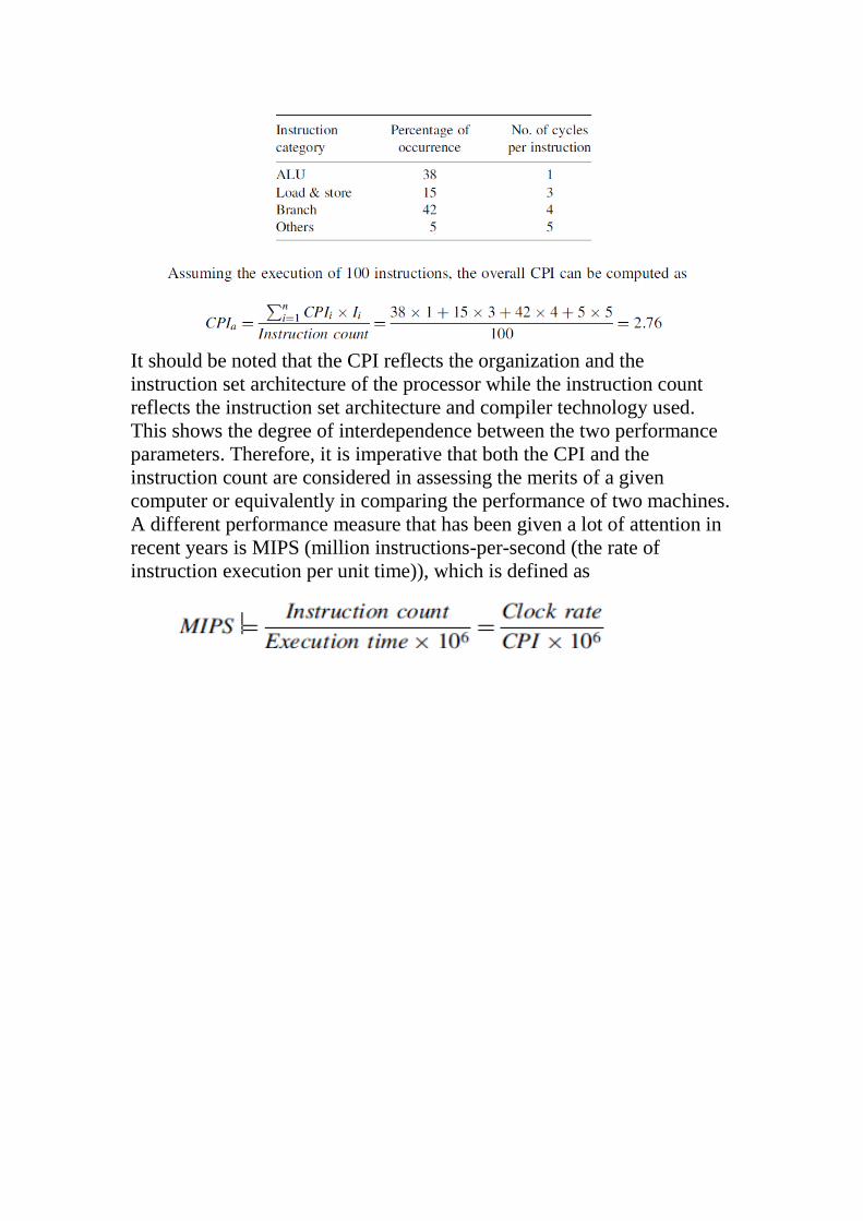
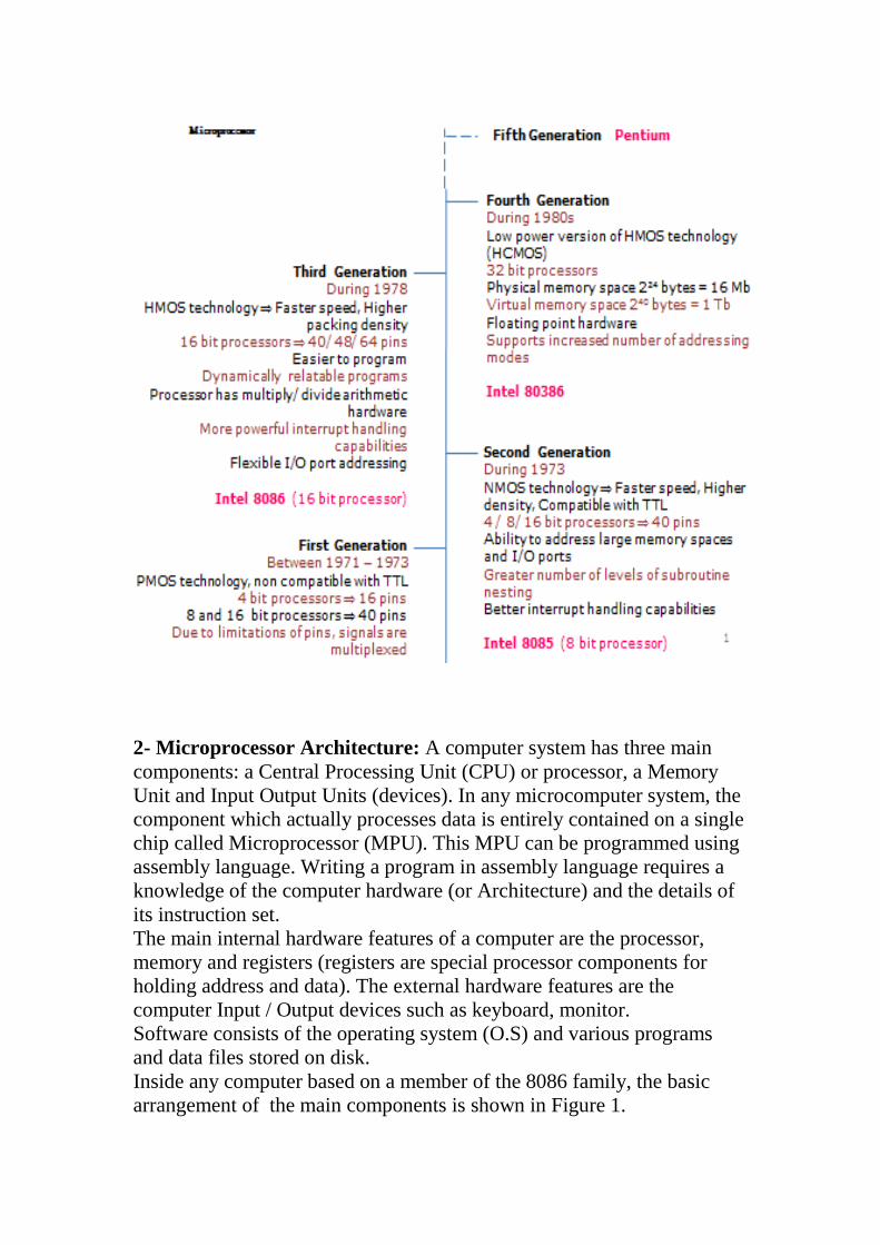
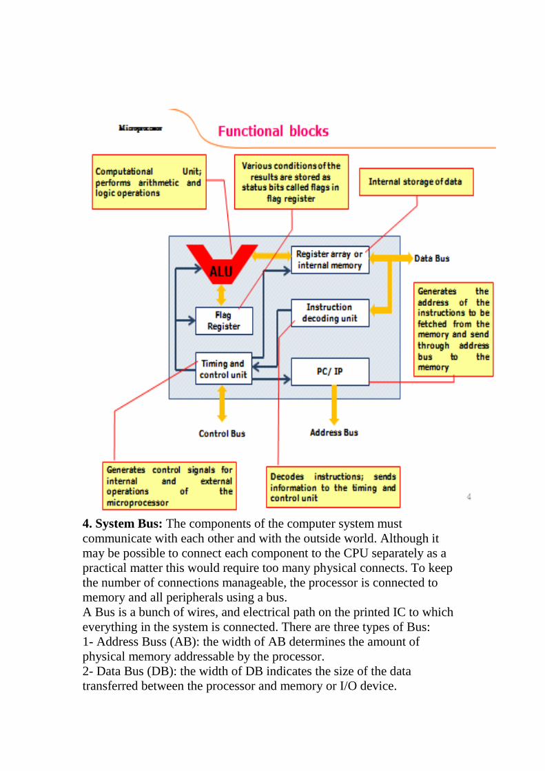
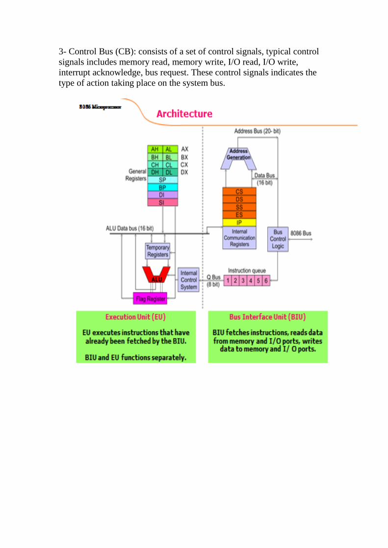
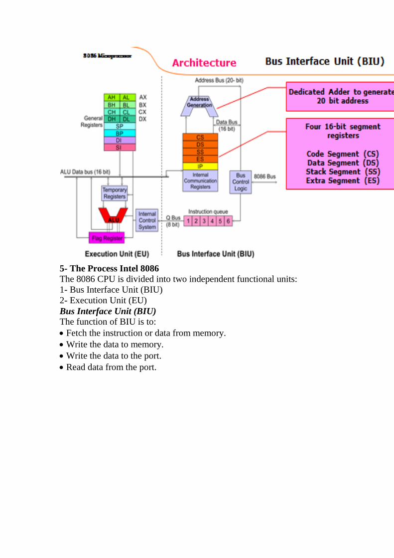
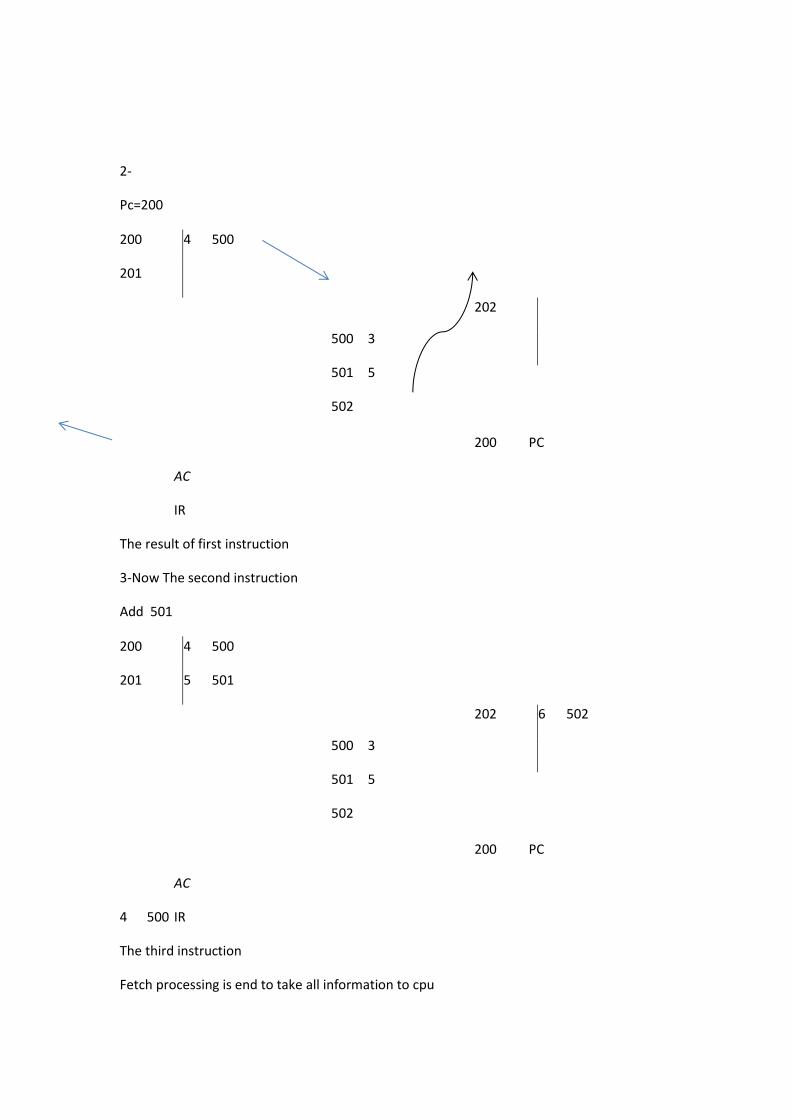
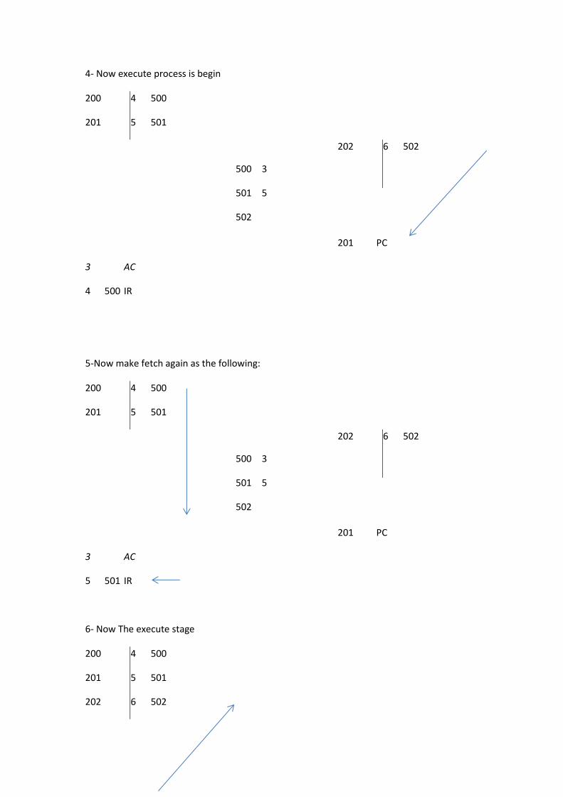
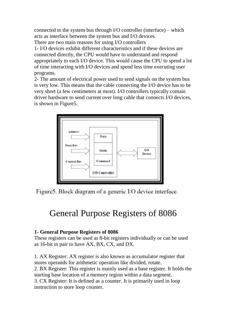
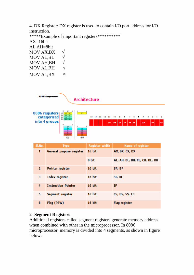
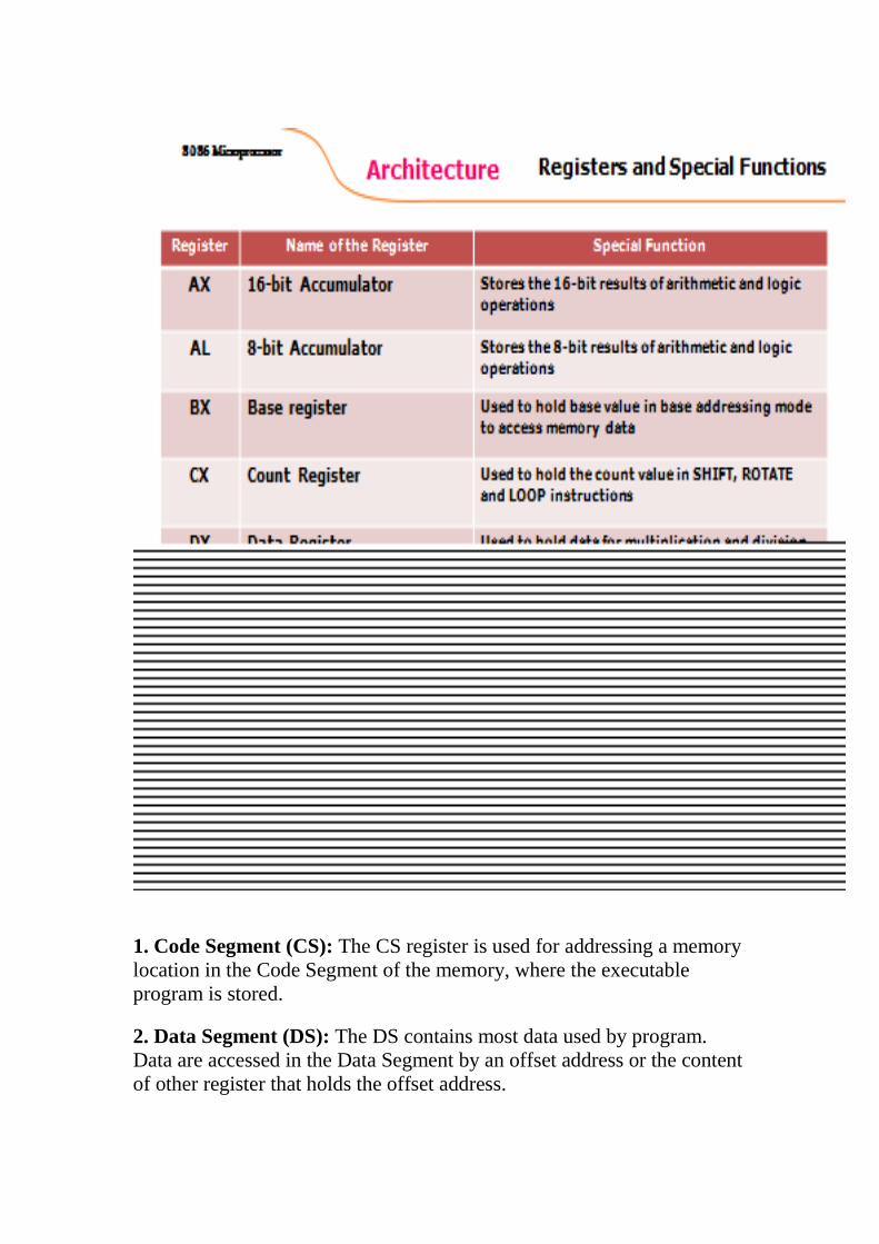
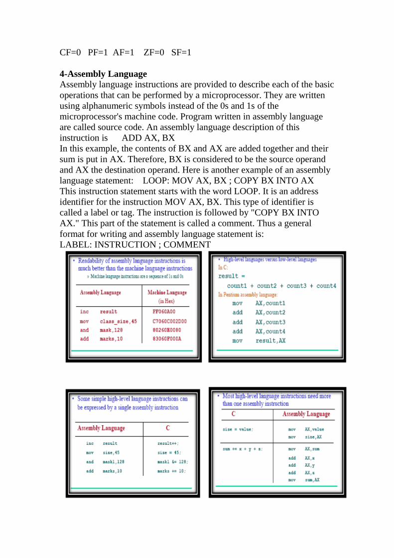
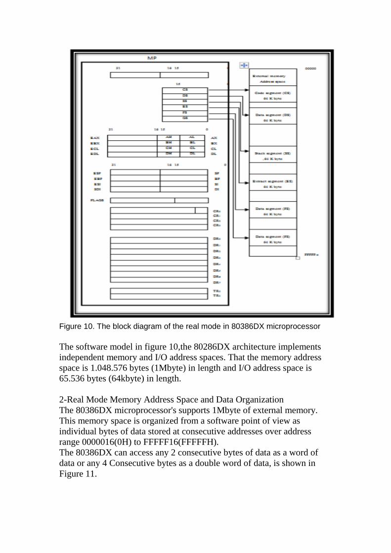
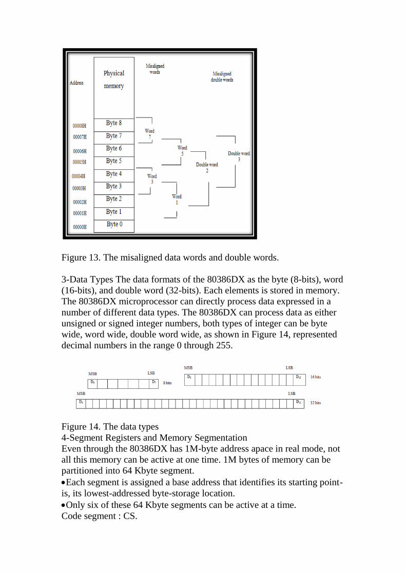
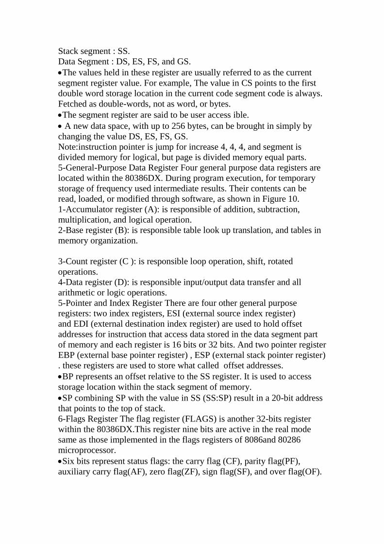
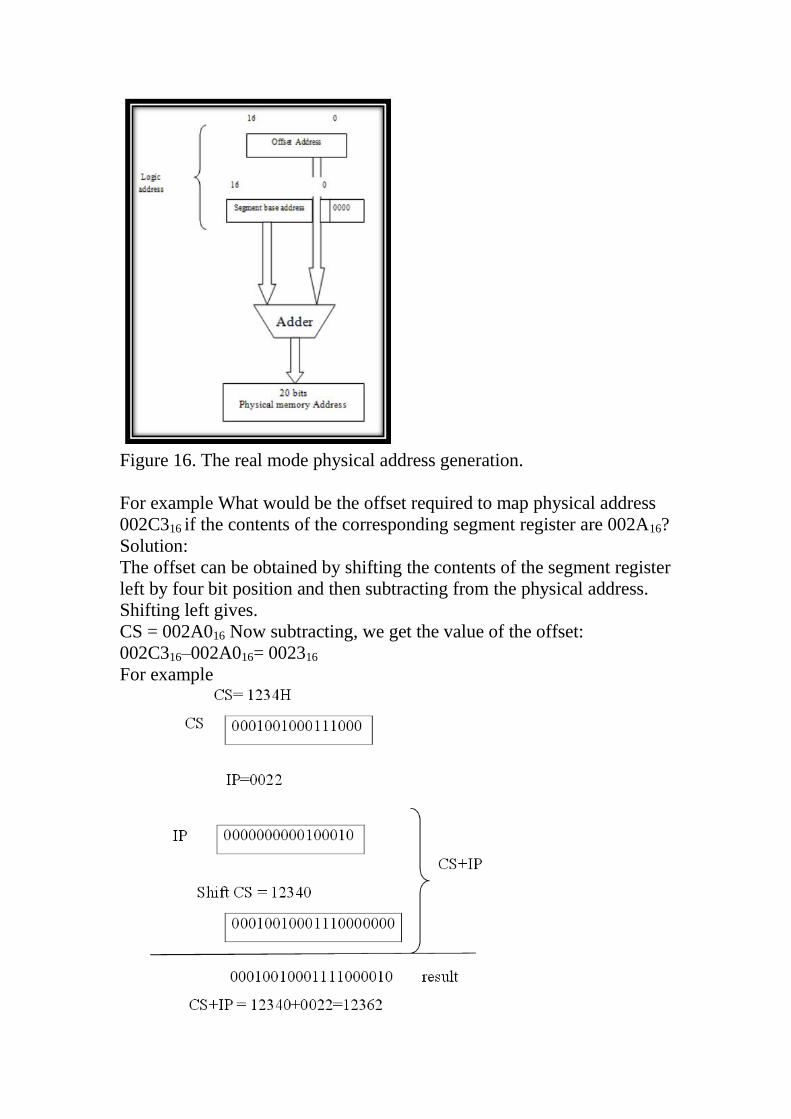
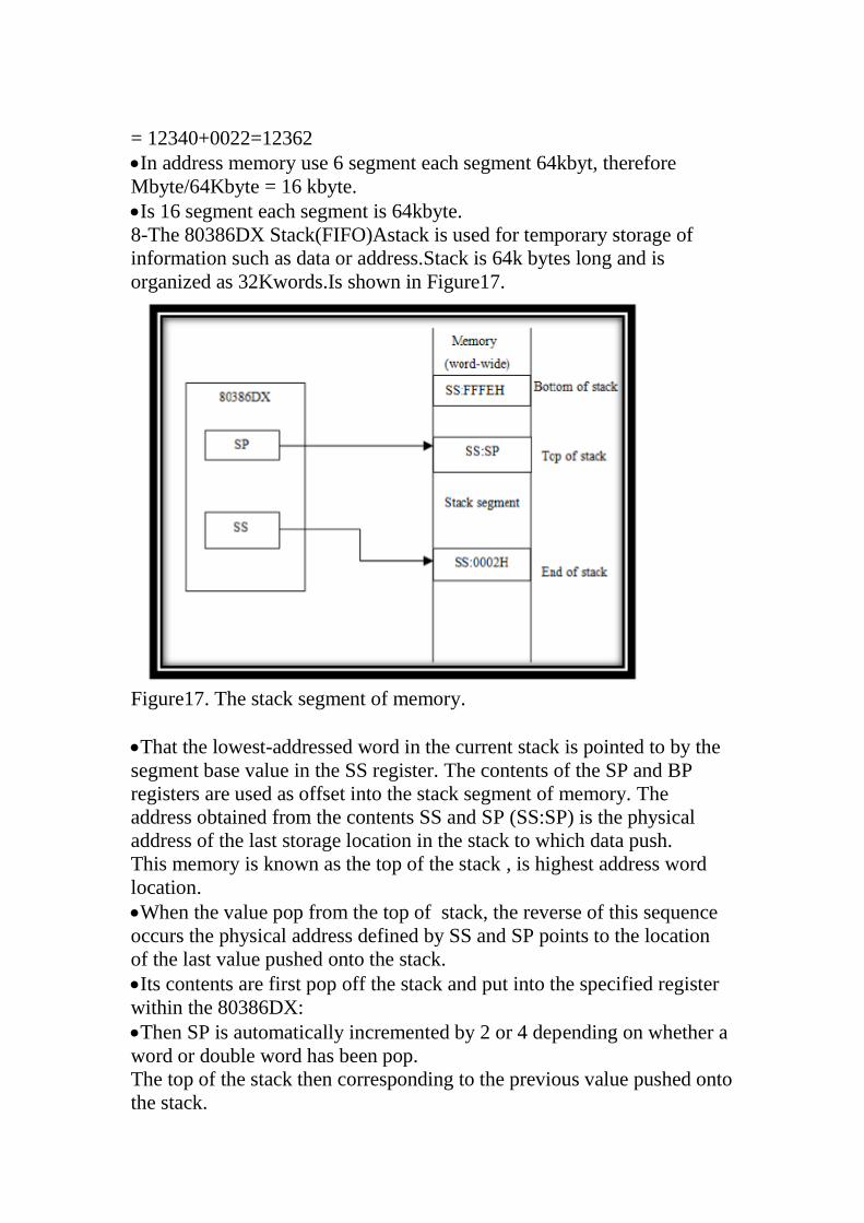
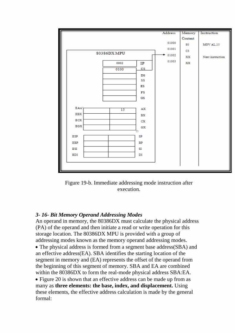
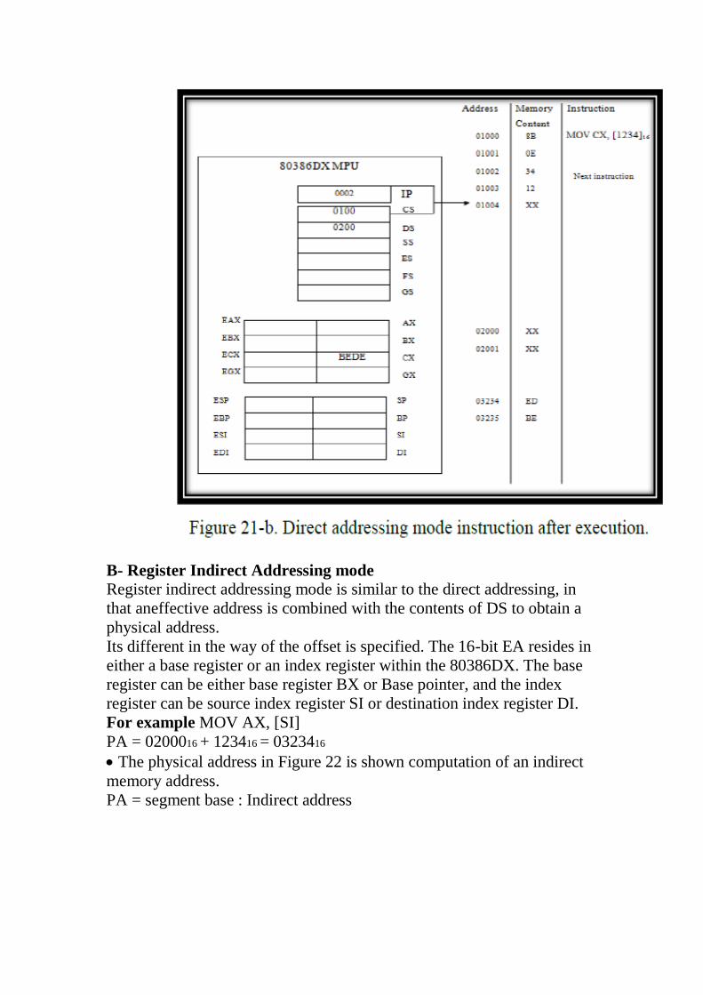
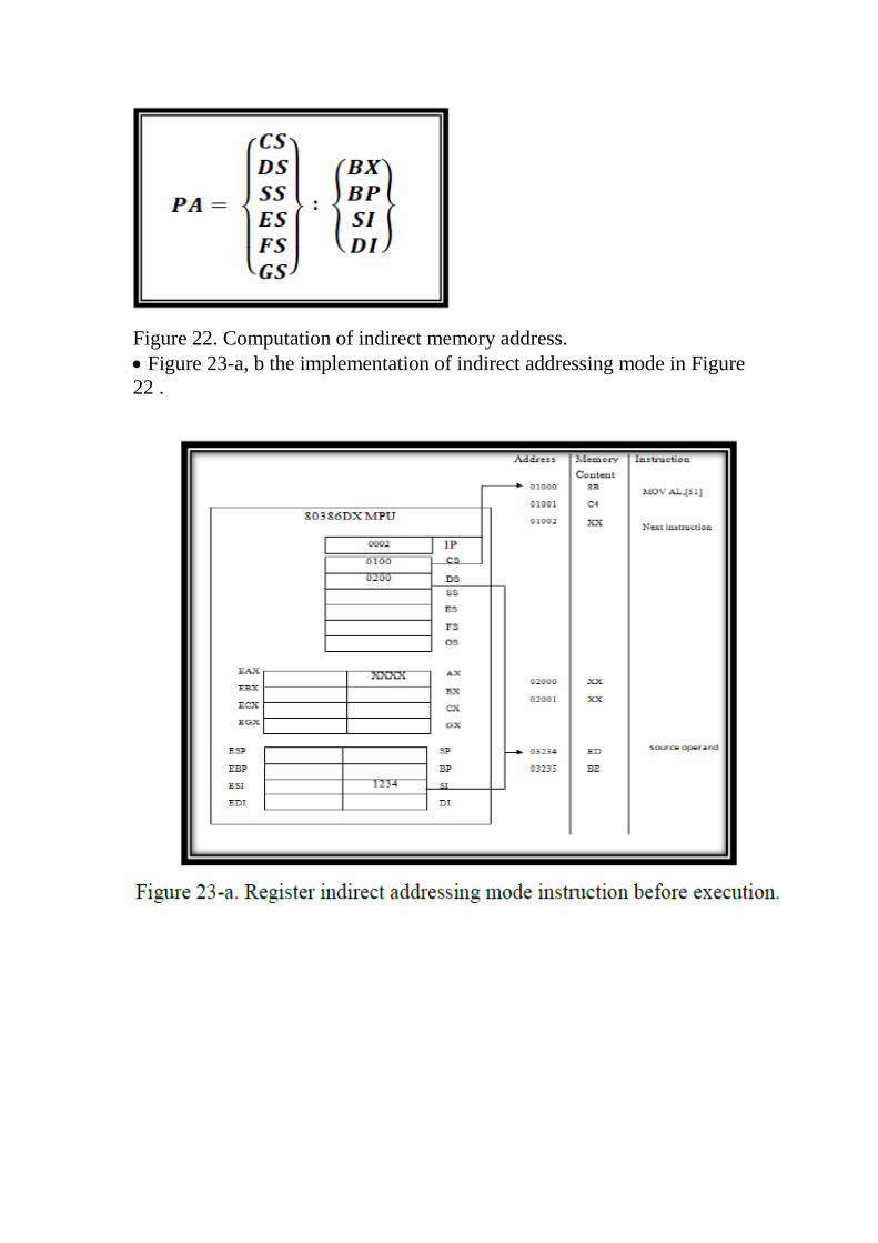
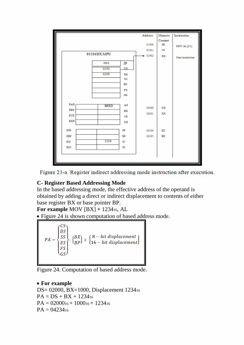
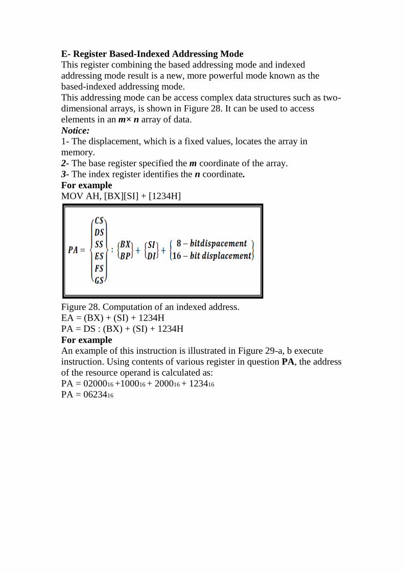
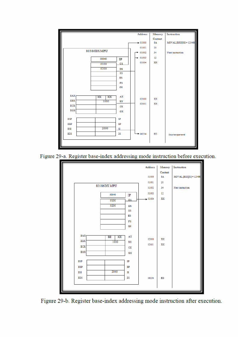
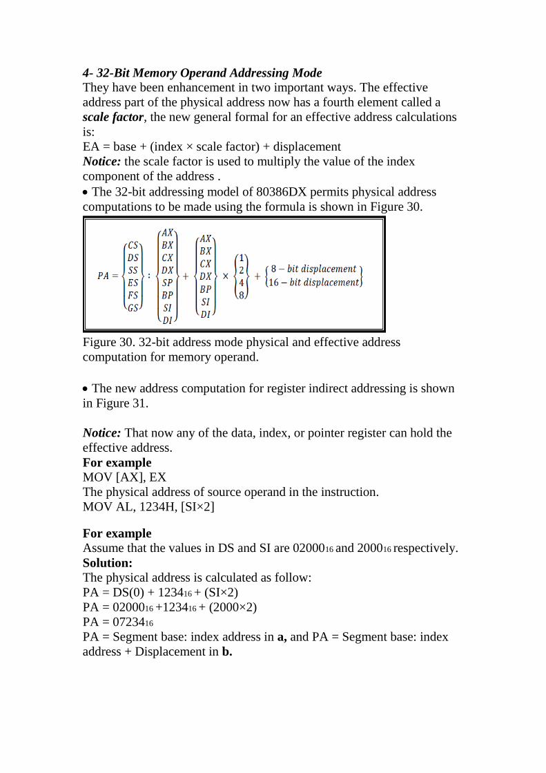
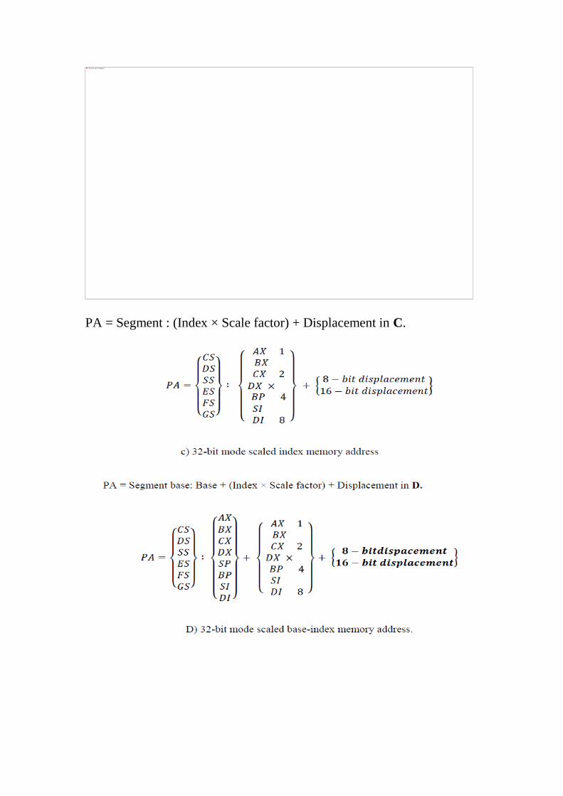
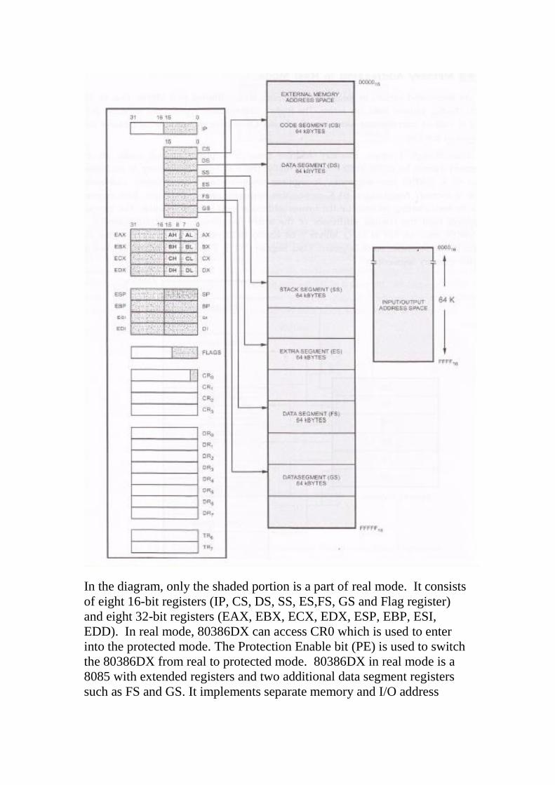
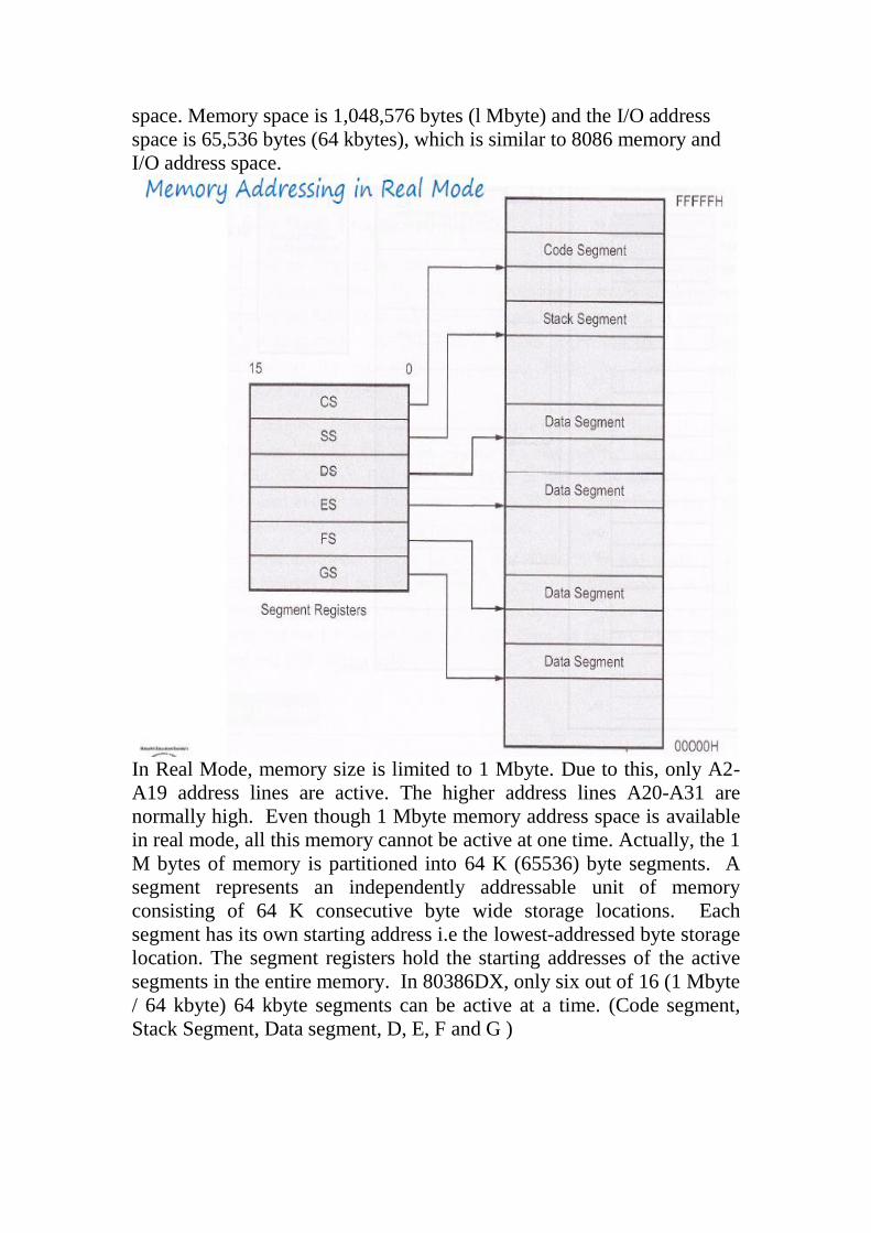
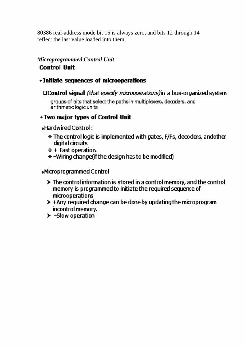
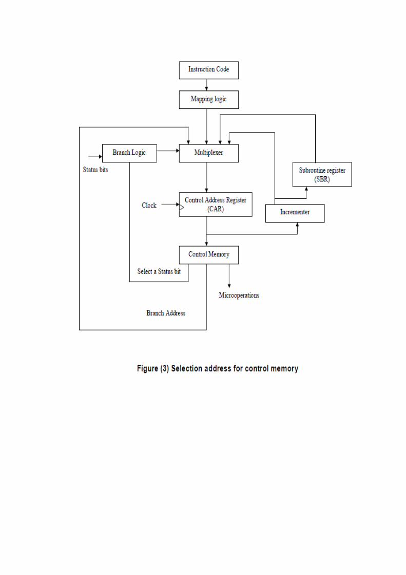
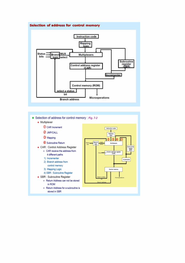
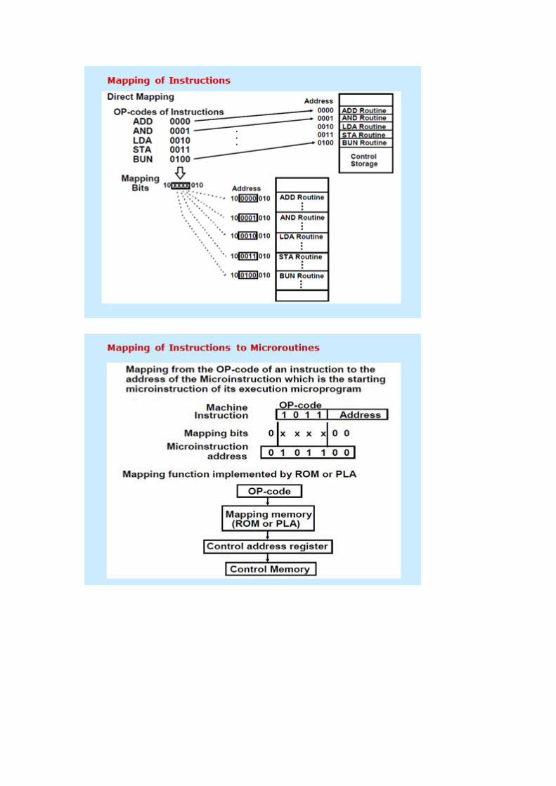

CHARACTERISTICS OF RISC
Common RISC Characteristics
- Operations are register-to-register with only LOAD and STORE
accessing memory
- The operations and addressing modes are reduced
Instruction formats are simple and do not cross word boundaries
- RISC branches avoid pipeline penalties - delayed branch
Characteristics of Initial RISC Machines
CHARACTERISTICS OF RISC
RISC Characteristics
-Relatively few instructions
- Relatively few addressing modes
- Memory access limited to load and store instructions
- All operations done within the registers of the CPU
- Fixed-length easily decoded instruction format
- Single-cycle instruction format
- Hardwired rather than microprogrammed control
Advantages of RISC
- VLSI Realization
- Computing Speed
- Design Costs and Reliability
- High Level Language Support
Pipeline And Vector Processing
- Cover
- is sw nw
-
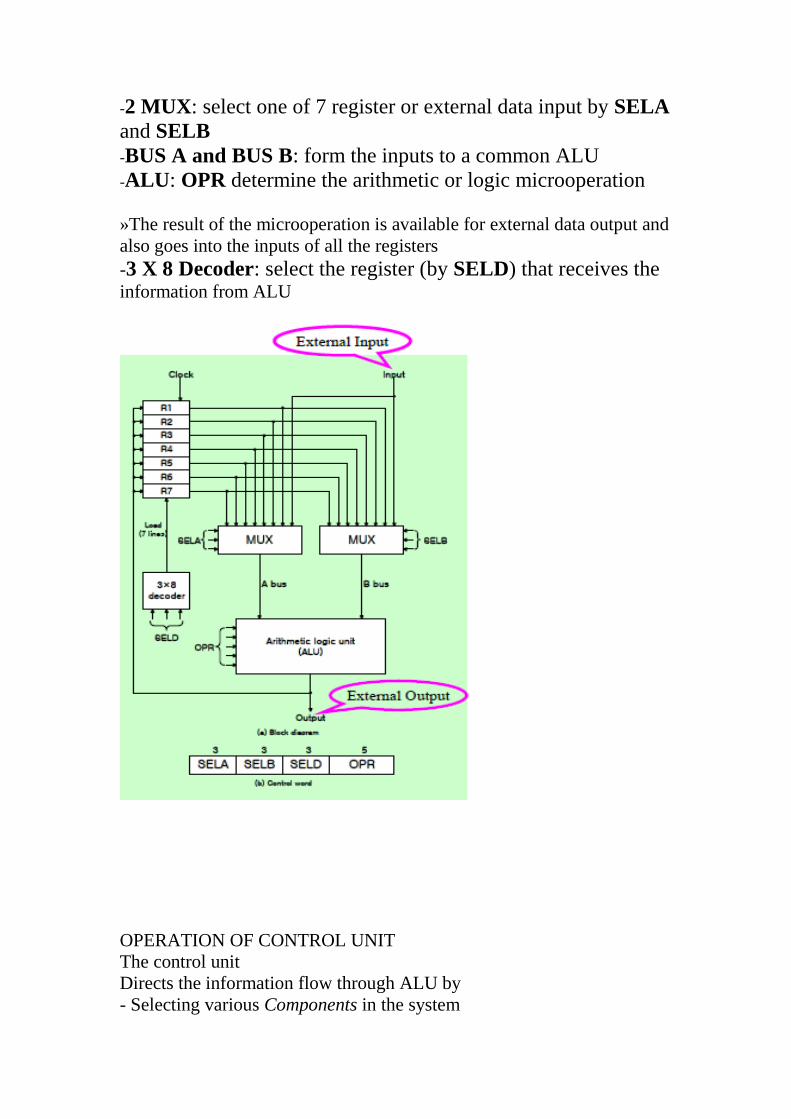
CHARACTERISTICS OF RISC
RISC Characteristics
-Relatively few instructions
- Relatively few addressing modes
- Memory access limited to load and store instructions
- All operations done within the registers of the CPU
- Fixed-length easily decoded instruction format
- Single-cycle instruction format
- Hardwired rather than microprogrammed control
Advantages of RISC
- VLSI Realization
- Computing Speed
- Design Costs and Reliability
- High Level Language Support
Pipeline And Vector Processing
- Cover
- is sw nw
-

Pipeline And Vector Processing
- Cover
- is sw nw
-
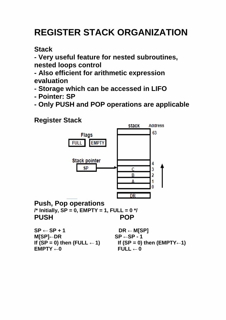
- Cover
- is sw nw
-