SARA-R5 series
44
UBX-19016638 - R07 C1-Public www.u-blox.com SARA-R5 series LTE-M / NB-IoT modules with secure cloud Data sheet Abstract Technical data sheet describing SARA-R5 LTE-M / NB-IoT modules, based on the u-blox UBX-R5 cellular chipset. The modules are a size-optimized solution specifically designed for IoT, integrating an in-house developed cellular modem, end-to-end trusted domain security, and u-blox’s leading GNSS technology. The modules deliver high performance satellite positioning alongside data connectivity in the very small and compact SARA form factor.
Transcript of SARA-R5 series

UBX-19016638 - R07
C1-Public www.u-blox.com
SARA-R5 series LTE-M / NB-IoT modules with secure cloud Data sheet
Abstract Technical data sheet describing SARA-R5 LTE-M / NB-IoT modules, based on the u-blox UBX-R5
cellular chipset. The modules are a size-optimized solution specifically designed for IoT, integrating
an in-house developed cellular modem, end-to-end trusted domain security, and u-blox’s leading
GNSS technology. The modules deliver high performance satellite positioning alongside data
connectivity in the very small and compact SARA form factor.

SARA-R5 series - Data sheet
UBX-19016638 - R07 Document information Page 2 of 44
C1-Public
Document information
Title SARA-R5 series
Subtitle LTE-M / NB-IoT modules with secure cloud
Document type Data sheet
Document number UBX-19016638
Revision and date R07 02-Oct-2020
Disclosure Restriction C1-Public
Product status Corresponding content status
Functional sample Draft For functional testing. Revised and supplementary data will be published later.
In development /
Prototype
Objective specification Target values. Revised and supplementary data will be published later.
Engineering sample Advance information Data based on early testing. Revised and supplementary data will be published later.
Initial production Early production information Data from product verification. Revised and supplementary data may be published later.
Mass production /
End of life
Production information Document contains the final product specification.
This document applies to the following products:
Product name Type number Modem version Application version PCN reference Product status
SARA-R500S SARA-R500S-00B-00 02.05 A00.01 UBX-20037360 Initial production
SARA-R510S SARA-R510S-00B-00 02.05 A00.01 UBX-20037360 Initial production
SARA-R510M8S SARA-R510M8S-00B-00 02.05 A00.01 UBX-20037360 Initial production
u-blox or third parties may hold intellectual property rights in the products, names, logos and designs included in this
document. Copying, reproduction, modification or disclosure to third parties of this document or any part thereof is only
permitted with the express written permission of u-blox.
The information contained herein is provided “as is” and u-blox assumes no liability for its use. No warranty, either express or
implied, is given, including but not limited to, with respect to the accuracy, correctness, reliability and fitness for a particular
purpose of the information. This document may be revised by u-blox at any time without notice. For the most recent
documents, visit www.u-blox.com.
Copyright © u-blox AG.

SARA-R5 series - Data sheet
UBX-19016638 - R07 Contents Page 3 of 44
C1-Public
Contents Document Information ................................................................................................................................ 2
Contents .......................................................................................................................................................... 3
1 Functional description ......................................................................................................................... 5
1.1 Overview ........................................................................................................................................................ 5
1.2 Product features ......................................................................................................................................... 6
1.3 Block diagram .............................................................................................................................................. 6
1.4 Product description .................................................................................................................................... 8
1.5 AT command support ................................................................................................................................ 9
1.6 Supported features .................................................................................................................................... 9
2 Interfaces ............................................................................................................................................... 12
2.1 Power management ..................................................................................................................................12
2.1.1 Module supply input (VCC) ..............................................................................................................12
2.1.2 Generic digital interfaces supply output (V_INT) ........................................................................12
2.2 Antenna interface ......................................................................................................................................12
2.2.1 Cellular antenna RF interface (ANT) ..............................................................................................12
2.2.2 GNSS antenna RF interface (ANT_GNSS) ....................................................................................12
2.2.3 Antenna detection (ANT_DET) .......................................................................................................12
2.3 System functions ...................................................................................................................................... 13
2.3.1 Module power-on .............................................................................................................................. 13
2.3.2 Module power-off .............................................................................................................................. 13
2.3.3 Module reset ...................................................................................................................................... 14
2.4 SIM ............................................................................................................................................................... 14
2.4.1 SIM interface ..................................................................................................................................... 14
2.4.2 SIM detection .................................................................................................................................... 14
2.5 Serial communication .............................................................................................................................. 14
2.5.1 UART interfaces ................................................................................................................................ 15
2.5.2 USB interface ..................................................................................................................................... 16
2.5.3 SPI interfaces ..................................................................................................................................... 17
2.5.4 SDIO interface .................................................................................................................................... 17
2.5.5 DDC (I2C) interface ............................................................................................................................ 17
2.6 Audio ............................................................................................................................................................. 17
2.7 GPIO ............................................................................................................................................................. 18
3 Pin definition ......................................................................................................................................... 19
3.1 Pin assignment .......................................................................................................................................... 19
4 Electrical specifications ................................................................................................................... 24
4.1 Absolute maximum rating....................................................................................................................... 24
4.1.1 Maximum ESD ................................................................................................................................... 24
4.2 Operating conditions ................................................................................................................................ 25
4.2.1 Operating temperature range ........................................................................................................ 25
4.2.2 Thermal parameters ........................................................................................................................ 25

SARA-R5 series - Data sheet
UBX-19016638 - R07 Contents Page 4 of 44
C1-Public
4.2.3 Supply/power pins ............................................................................................................................ 25
4.2.4 Current consumption ....................................................................................................................... 26
4.2.5 GNSS characteristics....................................................................................................................... 27
4.2.6 LTE RF characteristics .................................................................................................................... 28
4.2.7 ANT_DET pin ...................................................................................................................................... 29
4.2.8 Time pulse .......................................................................................................................................... 29
4.2.9 PWR_ON pin .......................................................................................................................................30
4.2.10 RESET_N pin ......................................................................................................................................30
4.2.11 SIM pins .............................................................................................................................................. 31
4.2.12 Generic Digital Interfaces pins ....................................................................................................... 31
4.2.13 DDC (I2C) pins .................................................................................................................................... 31
4.2.14 USB pins ............................................................................................................................................. 32
4.2.15 Smart temperature supervisor ...................................................................................................... 32
5 Mechanical specifications ............................................................................................................... 33
6 Qualification and approvals............................................................................................................. 34
6.1 Reliability tests .......................................................................................................................................... 34
6.1.1 Approvals ............................................................................................................................................ 34
7 Product handling & soldering .......................................................................................................... 35
7.1 Packaging ................................................................................................................................................... 35
7.1.1 Reels .................................................................................................................................................... 35
7.1.2 Tapes ................................................................................................................................................... 36
7.2 Moisture sensitivity levels ....................................................................................................................... 37
7.3 Reflow soldering ........................................................................................................................................ 37
7.4 ESD precautions ........................................................................................................................................ 37
8 Labeling and ordering information ............................................................................................... 38
8.1 Product labeling ......................................................................................................................................... 38
8.2 Explanation of codes ................................................................................................................................ 38
8.3 Ordering information ................................................................................................................................ 39
Appendix ....................................................................................................................................................... 40
A Glossary ................................................................................................................................................. 40
Related documents ................................................................................................................................... 43
Revision history .......................................................................................................................................... 43
Contact .......................................................................................................................................................... 44

SARA-R5 series - Data sheet
UBX-19016638 - R07 Functional description Page 5 of 44
C1-Public
1 Functional description
1.1 Overview
SARA-R5 series modules are secure cloud LTE Cat M1, LTE Cat NB2 solutions based on u-blox's
UBX-R5 cellular chipset. The SARA-R500 secure cloud module (called “SARA-R500S” in this data
sheet) is the cost effective solution, the SARA-R510 secure cloud module (called “SARA-R510S” in this
data sheet) is optimized for extremely low power consumption in deep-sleep PSM, and the
SARA-R510M8 secure cloud module (called “SARA-R510M8S” in this data sheet) has an integrated
u-blox M8 GNSS receiver chip and a separate GNSS antenna interface.
The miniature SARA LGA form factor (26.0 x 16.0 mm, 96-pin) allows an easy integration into compact
designs and a seamless drop-in migration from other u-blox cellular module families.
SARA-R5 series modules are form-factor compatible with the u-blox LISA, LARA and TOBY cellular
module families and they are pin-to-pin compatible with the u-blox SARA-R4, SARA-N2, SARA-N3,
SARA-N4, SARA-G3, SARA-G4 and SARA-U2 cellular modules families. This facilitates migration from
other u-blox LPWA modules as well as from other u-blox GSM/GPRS, CDMA, UMTS/HSPA and higher
LTE categories modules, maximizing customer investments, simplifying logistics, and enabling very
short time-to-market.
SARA-R5 series modules provide software-based multi-band configurability enabling international
multi-regional coverage in LTE Cat M1 / NB2 radio access technologies, supporting a comprehensive
set of 3GPP Rel. 14 features that are relevant for IoT applications.
SARA-R5 series modules offer data communications up to 1200 kbit/s over an extended operating
temperature range of –40 °C to +85 °C, with low power consumption, and with coverage enhancement
for deeper range into buildings and basements (and underground with NB2).
With a discrete, hardware-based secure element and a lightweight pre-shared key management
system, u-blox offers state-of-the-art security that is ideal for IoT applications and includes local data
protection, zero touch provisioning, anti-cloning, and local secure chip-to-chip communication. With
many interface options and an integrated IP stack, SARA-R5 series modules are the optimal choice
for LPWA applications with low to medium data throughput rates, as well as devices that require long
battery lifetimes, such as used in smart metering, smart lighting, telematics, asset tracking, remote
monitoring, alarm panels, and connected healthcare.
Customers can future-proof their solutions by means of over-the-air firmware updates, thanks to the
uFOTA client/server solution that utilizes LwM2M, a light and compact protocol ideal for IoT.
The “00” products version of the SARA-R5 series modules do not support LTE NB-IoT.

SARA-R5 series - Data sheet
UBX-19016638 - R07 Functional description Page 6 of 44
C1-Public
1.2 Product features
Model Region RAT Positioning Interfaces Features Grade
LT
E c
ate
go
ry
LT
E F
DD
ba
nd
s
Inte
gra
ted
GN
SS
re
ce
ive
r
Ex
tern
al G
NS
S c
on
tro
l via
mo
de
m
As
sis
tNo
w s
oft
wa
re
Ce
llL
oc
ate
®
UA
RT
s
US
B (
for
dia
gn
os
tic
s)
SP
I
SD
IO
DD
C (
I2C
)
GP
IOs
Dig
ita
l au
dio
(I2
S)
Se
cu
re C
lou
d s
erv
ice
s V
er
1.1
Em
be
dd
ed
Se
cu
re E
lem
en
t E
AL
5+
Hig
h c
ert
ifie
d
An
ten
na
dy
na
mic
tu
nin
g
Ce
llT
ime
®
Ult
ra-l
ow
po
we
r c
on
su
mp
tio
n in
PS
M
Em
be
dd
ed
TC
P/U
DP
sta
ck
Em
be
dd
ed
HT
TP
, FT
P
Em
be
dd
ed
TL
S, D
TL
S
FW
up
da
te v
ia s
eri
al
(FO
AT
)
u-b
lox
Fir
mw
are
up
da
te O
ve
r th
e A
ir (
uF
OT
A)
Lw
M2
M w
ith
dy
na
mic
all
y lo
ad
ed
ob
jec
ts
Em
be
dd
ed
MQ
TT
, MQ
TT
-SN
Em
be
dd
ed
Co
AP
La
st
ga
sp
Ja
mm
ing
de
tec
tio
n
An
ten
na
an
d S
IM d
ete
cti
on
Sta
nd
ard
Pro
fes
sio
na
l
Au
tom
oti
ve
SARA-R500S Multi
Region
M1
NB2 *
SARA-R510S Multi
Region
M1
NB2 *
SARA-R510M8S Multi
Region
M1
NB2 *
* = LTE Bands 1, 2, 3, 4, 5, 8, 12, 13, 18, 19, 20, 26, 28 in M1 and NB2, LTE bands 25 in M1-only, and LTE bands 66, 71, 85 in NB2-only
= supported by all FW versions = supported by future FW versions
Table 1: SARA-R5 series main features summary
The “00” products version of the SARA-R5 series modules do not support LTE NB-IoT.
1.3 Block diagram
V_INT (I/O)
VCC (supply)
ANT_DET
ANT
Flash memory
SIM
I2S
GPIOs
Reset
Power-on
UART
USB
DDC (I2C)
PA
UBX-R5 Cellular chipset
Base Bandprocessor
Power Management
Unit
RF transceiver
Filter
Filter
Switch
SPI
SDIO
Secure element (eSIM)
32 kHz
26 MHz
TCXO
Figure 1: SARA-R500S block diagram

SARA-R5 series - Data sheet
UBX-19016638 - R07 Functional description Page 7 of 44
C1-Public
V_INT (I/O)
VCC (supply)
ANT_DET
ANT
Flash memory
SIM
I2S
GPIOs
Reset
Power-on
UART
USB
DDC (I2C)
PA
UBX-R5 Cellular chipset
Base Bandprocessor
Power Management
Unit
RF transceiver
Filter
Filter
Switch
SPI
SDIO
Secure element (eSIM)
RTC
32 kHz
26 MHz
TCXO
Figure 2: SARA-R510S block diagram
ANT_GNSS
V_INT (I/O)
VCC (supply)
ANT_DET
ANT
Flash memory
SIM
I2S
GPIOs
Reset
Power-on
UART
USB
DDC (I2C)
PA
UBX-R5 Cellular chipset
Base Bandprocessor
Power Management
Unit
RF transceiver
Filter
Filter
Switch
SAW LNA UBX-M8GNSS chipset
SPI
SDIO
Secure element (eSIM)
32 kHz
26 MHz
TCXO
Figure 3: SARA-R510M8S block diagram
The “00” products version of the SARA-R5 series modules do not support the following interfaces,
which should be left unconnected and should not be driven by external devices:
o SPI interface
o SDIO interface
o Digital audio (I2S) interface

SARA-R5 series - Data sheet
UBX-19016638 - R07 Functional description Page 8 of 44
C1-Public
1.4 Product description
SARA-R5 series modules include the following variants / products versions:
• SARA-R500S LTE Cat M1 / NB2 module for multi-region use, cost effective solution for devices
that do not need to reach ultra-low power consumption in deep-sleep power saving mode (PSM)
• SARA-R510S LTE Cat M1 / NB2 module for multi-region use, designed to achieve extremely low
current consumption in deep-sleep power saving mode (PSM)
• SARA-R510M8S LTE Cat M1 / NB2 module for multi-region use, integrating the UBX-M8030 high
performance standard precision concurrent GNSS chip for global position acquisition
Item SARA-R500S / SARA-R510S SARA-R510M8S
Cellular protocol stack 3GPP Release 13 LTE Cat M1 and NB1
3GPP Release 14 LTE Cat M1: Coverage
Enhancement Mode B, Uplink TBS of 2984b
3GPP Release 14 LTE Cat NB2: Higher data
rate (TBS of 2536b), Mobility enhancement
(RRC connection re-establishment), E-Cell
ID, Lower power class PC6 (14dBm), two
HARQ processes, Release Assistant,
Random access on Non-Anchor Carrier
3GPP Release 13 LTE Cat M1 and NB1
3GPP Release 14 LTE Cat M1: Coverage
Enhancement Mode B, Uplink TBS of 2984b
3GPP Release 14 LTE Cat NB2: Higher data
rate (TBS of 2536b), Mobility enhancement
(RRC connection re-establishment), E-Cell
ID, Lower power class PC6 (14dBm), two
HARQ processes, Release Assistant,
Random access on Non-Anchor Carrier
Cellular Radio Access Technology LTE Cat M1 Half-Duplex
LTE Cat NB2 Half-Duplex
LTE Cat M1 Half-Duplex
LTE Cat NB2 Half-Duplex
Cellular operating bands LTE FDD band 1 (2100 MHz)
LTE FDD band 2 (1900 MHz)
LTE FDD band 3 (1800 MHz)
LTE FDD band 4 (1700 MHz)
LTE FDD band 5 (850 MHz)
LTE FDD band 8 (900 MHz)
LTE FDD band 12 (700 MHz)
LTE FDD band 13 (750 MHz)
LTE FDD band 18 (850 MHz)
LTE FDD band 19 (850 MHz)
LTE FDD band 20 (800 MHz)
LTE FDD band 25 (1900 MHz) 1
LTE FDD band 26 (850 MHz)
LTE FDD band 28 (700 MHz)
LTE FDD band 66 (1700 MHz) 2
LTE FDD band 71 (600 MHz) 2
LTE FDD band 85 (700 MHz) 2
LTE FDD band 1 (2100 MHz)
LTE FDD band 2 (1900 MHz)
LTE FDD band 3 (1800 MHz)
LTE FDD band 4 (1700 MHz)
LTE FDD band 5 (850 MHz)
LTE FDD band 8 (900 MHz)
LTE FDD band 12 (700 MHz)
LTE FDD band 13 (750 MHz)
LTE FDD band 18 (850 MHz)
LTE FDD band 19 (850 MHz)
LTE FDD band 20 (800 MHz)
LTE FDD band 25 (1900 MHz) 1
LTE FDD band 26 (850 MHz)
LTE FDD band 28 (700 MHz)
LTE FDD band 66 (1700 MHz) 2
LTE FDD band 71 (600 MHz) 2
LTE FDD band 85 (700 MHz) 2
Cellular power class LTE power class 3 (23 dBm) LTE power class 3 (23 dBm)
Cellular data rate LTE category M1:
up to 1200 kbit/s UL
up to 375 kbit/s DL
LTE category NB2:
up to 140 kbit/s UL
up to 125 kbit/s DL
LTE category M1:
up to 1200 kbit/s UL
up to 375 kbit/s DL
LTE category NB2:
up to 140 kbit/s UL
up to 125 kbit/s DL
GNSS receiver type - 72-channel u-blox M8 engine
GPS L1C/A, SBAS L1C/A, QZSS L1C/A,
QZSS L1-SAIF, GLONASS L10F, BeiDou B1I,
Galileo E1B/C
Table 2: SARA-R5 series cellular and GNSS main characteristics
The “00” products version of the SARA-R5 series modules do not support LTE NB-IoT.
1 Not supported in LTE category NB2 2 Not supported in LTE category M1

SARA-R5 series - Data sheet
UBX-19016638 - R07 Functional description Page 9 of 44
C1-Public
1.5 AT command support
The SARA-R5 series modules support AT commands according to the 3GPP standards TS 27.007 [4],
TS 27.005 [5], TS 27.010 [6], and the u-blox AT commands extension.
For the complete list of all supported AT commands and their syntax, see SARA-R5 series AT
commands manual [1].
1.6 Supported features
Table 3 lists some of the main features supported by SARA-R5 series modules. For more details, see
the SARA-R5 series system integration manual [2] and SARA-R5 series AT commands manual [1].
Feature Description
Device security An immutable chip ID and hardware-based Root of Trust (RoT) embedded in a dedicated
Common Criteria EAL5+ high certified secure element provide foundational security and a
unique device identity.
Device security features include:
• Secure boot: guarantees software authenticity and integrity
• Secure update: secure delivery of the correct FW to the module
• Anticloning detection and rejection: system automatically identifies and blocks clones that
use the same RoT
Data security Secure libraries allow generation of hardware-backed crypto functions and keys for local
encryption to secure local file storage and for end-to-end encryption.
Data security features include:
• Local data protection: symmetric crypto functions via AT command to locally encrypt /
decrypt and authenticate data (e.g. certificates, tokens) on the device. Allows also secure
local storage of sensitive information in a non-secure location (e.g. in “standard” device
memory)
• Local chip-to-chip (C2C) security: unique cryptographic pairing between the MCU of the
device and u-blox module by providing confidentiality, integrity, mutual authentication for
their communication channel (e.g. UART interface)
• E2E symmetric KMS: highly scalable method to provision and manage a session unique PSK
available in cloud via REST API. Up to 8 times reduction in secure communication data
overhead reducing data power consumption and cost
• E2E data protection: minimize data traffic and power encrypting data on a device and
decrypting asynchronously in cloud independent of protocols, servers, platforms or time
before reaching final destination
Access management Allow only authenticated access to device and features, safely manage changes of device
ownership and provide out-of-the-box, simple, secure and cost effective zero touch onboarding
to popular IoT cloud platforms.
Access management features include:
• Change of ownership: efficient way to change the ownership and to apply the
policies / authorizations of the new owner, even if the device is already in the field
• Zero touch provisioning for AWS and Azure: out-of-the-box, simple, secure and cost effective
AWS and Azure onboarding
Integrated GNSS receiver 3 SARA-R510M8S modules are pre-integrated with a u-blox UBX-M8030 concurrent GNSS
chipset with SPG 3.01 firmware version, comprehensive of a dedicated GNSS antenna interface,
additional LNA and SAW filter for a highly reliable, accurate positioning data.
The GNSS system is totally independent from the LTE system and can run concurrently to a
LTE communication.
External GNSS control via
modem 4
Full access to external u-blox positioning chips and modules through DDC (I2C) interface.
This means that any host processor can control the SARA-R500S or SARA-R510S cellular
module and the u-blox positioning chip or module through a single serial port.
3 Not supported by SARA-R500S / SARA-R510S modules. 4 Not supported by SARA-R510M8S modules.

SARA-R5 series - Data sheet
UBX-19016638 - R07 Functional description Page 10 of 44
C1-Public
Feature Description
Embedded AssistNow
Software
Embedded AssistNow Online and AssistNow Offline clients are available to provide better GNSS
performance and faster Time-to-First-Fix. An AT command can enable / disable the clients.
CellLocate® Enables the estimation of device position based on the parameters of the mobile network cells
visible to the specific device based on the CellLocate® database.
CellLocate® is available via a set of AT commands for CellLocate® service configuration and
position request.
Hybrid Positioning Provides the module’s current position using a u-blox positioning chip or module (external for
SARA-R500S / SARA-R510S, integrated UBX-M8 chip for SARA-R510M8S) or the estimated
position from CellLocate®, depending on which positioning method provides the best and
fastest solution according to the user configuration.
Hybrid positioning is implemented through a set of AT commands that allow the configuration
and the position request.
CellTime® Returns accurate timing retrieved from the LTE network and/or from the u-blox positioning chip
or module (external for SARA-R500S / SARA-R510S, integrated UBX-M8 chip for
SARA-R510M8S).
Can be used to provide periodic time-stamps to an external application processor or to output a
time indication associated to an interrupt detected on a GPIO (e.g. coming from an external
sensor connected to the module).
The implementation of CellTime® can be extended to control and maintain timing info in a
network of sensors (each one integrating a SARA-R5 module).
Antenna dynamic tuning Control via two GPIOs an external antenna matching IC according to the LTE band used by the
module.
Embedded TCP and UDP
stack
Embedded TCP/IP and UDP/IP stack including direct link mode for TCP and UDP sockets.
Sockets can be set in Direct Link mode to establish a transparent end-to-end communication
with an already connected TCP or UDP socket via the serial interface.
HTTP, HTTPS
(v1.0 for +UHTTP,
v1.1 for LwM2M client)
Hyper-Text Transfer Protocol as well as Secure Hyper-Text Transfer Protocol (SSL encryption)
functionalities are supported via AT commands.
FTP, FTPS File Transfer Protocol as well as Secure File Transfer Protocol (SSL encryption of FTP control
channel) functionalities are supported by means of AT commands.
CoAP
(RFC 7252) [11]
Embedded Constrained Application Protocol (CoAP) datagram-based client/server application
protocol designed to easily translate from HTTP for simplified integration with the web.
MQTT (v3.1.1) and
MQTT-SN (v1.2)
Embedded Message Queuing Telemetry Transport (MQTT) and MQTT for Sensor Networks
(MQTT-SN) publish-subscribe messaging protocols designed for lightweight M2M
communications over TCP (MQTT) or over UDP (MQTT-SN). These allow one-to-one, one-to-
many and many-to-one communications over a TCP or UDP connection.
LwM2M with dynamically
loaded objects (v1.0)
The LwM2M is a light and compact communication protocol designed for managing IoT
machine-to-machine communication between a LwM2M Server and a LwM2M Client located in
lightweight, low power or resource-constrained LwM2M devices, with object data model.
SARA-R5 series modules allow customers to configure dynamically loaded run time objects,
defining necessary custom objects, creating instances of those objects as appropriate,
managing module LwM2M protocol stack to interact with the LwM2M server.
TLS (v1.0, v1.1, v1.2) and
DTLS (v1.2)
Transport Layer Security (TLS) provides security for HTTP, FTP, MQTT and TCP
communications.
Embedded Datagram Transport Layer Security (DTLS) provides security for CoAP, LwM2M,
MQTT-SN and UDP communications.
Jamming detection Detects “artificial” interference that obscures the operator’s carrier entitled to give access to
the radio service and automatically reports the start and stop of such conditions to the
application processor that can react accordingly.
Smart temperature
supervisor
Constant monitoring of the module board temperature:
• Warning notification when the temperature approaches an upper or lower predefined
threshold (see section 4.2.15)
• Shutdown notified and forced when the temperature value is outside the specified range
(shutdown suspended in case of an emergency call in progress)
The smart temperature supervisor feature can be enabled or disabled through an AT command
(see the SARA-R5 series AT commands manual [1], +USTS AT command).

SARA-R5 series - Data sheet
UBX-19016638 - R07 Functional description Page 11 of 44
C1-Public
Feature Description
Last gasp In case of power supply outage (i.e. main supply interruption, battery removal, battery voltage
below a certain threshold) the cellular module can be configured to send an alarm notification to
a remote entity. The feature can be enabled and configured through the +ULGASP AT
command.
Network status indication GPIO configured to indicate the network status: registered home network, registered roaming,
data call enabled, no service. The feature can be enabled through the +UGPIOC AT command.
Antenna detection The ANT_DET pin provides antenna presence detection capability, evaluating the resistance
from the ANT pin to GND by means of an external antenna detection circuit implemented on the
application board. The antenna supervisor (i.e. antenna detection) feature can be enabled
through the +UANTR AT command.
BIP Bearer Independent Protocol for over-the-air SIM provisioning.
Dual stack IPv4/Ipv6 Capability to move between Ipv4 and dual stack network infrastructures.
Ipv4 and Ipv6 addresses can be used.
Firmware update Over AT
commands (FOAT)
Firmware module update over AT command interface.
The feature can be enabled and configured through the +UFWUPD AT command.
u-blox Firmware update
Over The Air (uFOTA)
u-blox firmware module update over the LTE air interface client/server solution using LwM2M.
Power Saving Mode (PSM) The Power Saving Mode (PSM) feature, defined in 3GPP Rel.13, allows further reduction of the
module current consumption maximizing the amount of time a device can remain in PSM low
power deep-sleep mode during periods of data inactivity. It can be activated and configured by
the +CPSMS AT command.
eDRX Extended mode DRX, based on 3GPP Rel.13, reduces the amount of signaling overhead
decreasing the frequency of scheduled measurements and/or transmissions performed by the
module in idle mode. This in turn leads to a reduction in the module power consumption while
maintaining a perpetual connection with the base station.
Coverage Enhancement
(mode A and mode B)
Coverage Enhancement modes introduced in 3GPP Rel.13 are used to improve the cell signal
penetration.
LTE-M and NB-IoT 3GPP
release 14 features
For LTE-M: Larger max UL TBS (2984 bits instead of 1000 bits), Enhanced PUCCH repetition in
CE mode B (64 and 128 repetition factor)
For NB-IoT: Cat-NB2 higher data rate (with 2536 bit TBS), Release assistance indication, Power
class 6 (maximum transmit power of 14 dBm) configurable by dedicated AT command, RRC
connection re-establishment for the control plane CIoT EPS optimization, 2 UL/DL HARQ
processes, Non-anchor paging and RACH, E-CID positioning
Table 3: Some of the main features supported by SARA-R5 series modules
The “00” products version of the SARA-R5 series modules do not support LTE NB-IoT.

SARA-R5 series - Data sheet
UBX-19016638 - R07 Interfaces Page 12 of 44
C1-Public
2 Interfaces
2.1 Power management
2.1.1 Module supply input (VCC)
SARA-R5 series modules must be supplied through the VCC pins by a proper external DC power supply
providing a nominal voltage within the normal operating range (see Table 10). Voltage must be stable,
because during operation the current drawn from VCC may vary significantly, based on the power
consumption profile of the LTE Cat M1 and LTE Cat NB2 radio access technologies (described in the
SARA-R5 series system integration manual [2]).
The three VCC pins of SARA-R5 series modules are internally connected to both the internal Power
Amplifier and the internal Power Management Unit, which integrates voltage regulators generating
all the internal supply voltages needed by the module for the designed operations, as the supply
voltage for the generic digital interfaces (V_INT), the supply voltage for the SIM interface (VSIM), and
the supply voltage for the internal GNSS receiver.
It is important that the system power supply circuit is able to withstand the maximum pulse current
during a transmit burst at maximum power level (see Table 12).
2.1.2 Generic digital interfaces supply output (V_INT)
SARA-R5 series modules provide a 1.8 V supply rail output on the V_INT pin, which is internally
generated when the module is switched on. The same voltage domain is used internally to supply the
generic digital interfaces of the module. The V_INT supply output can be used in place of an external
discrete regulator.
It is recommended to provide accessible test point directly connected to the V_INT pin.
2.2 Antenna interface
2.2.1 Cellular antenna RF interface (ANT)
The ANT pin is the cellular RF antenna I/O interface, designed with 50 characteristic impedance.
2.2.2 GNSS antenna RF interface (ANT_GNSS)
The GNSS antenna RF interface is not supported by SARA-R500S and SARA-R510S modules.
The ANT_GNSS pin represents the GNSS RF input of the SARA-R510M8S modules, designed with
50 characteristic impedance and with an internal DC block, suitable for both active and/or passive
GNSS antennas due to the built-in SAW filter followed by an LNA in front of the integrated high
performing u-blox M8 concurrent positioning engine.
2.2.3 Antenna detection (ANT_DET)
The ANT_DET pin is an Analog to Digital Converter (ADC) input with a current source provided by
SARA-R5 series modules to sense the external antenna presence (as an optional feature), evaluating
the DC resistance to GND by means of an externally implemented circuit (for more details, see the
u-blox SARA-R5 series system integration manual [2] and the SARA-R5 series AT commands
manual [1]).

SARA-R5 series - Data sheet
UBX-19016638 - R07 Interfaces Page 13 of 44
C1-Public
2.3 System functions
2.3.1 Module power-on
When the SARA-R500S and SARA-R510M8S modules are not powered, they can be switched on as
following:
• Applying a voltage at the VCC module supply input within the operating range (see Table 10)
When the SARA-R510S modules are not powered, they can be switched on as following:
• Applying a voltage at the VCC module supply input within the operating range (see Table 10), and
then forcing a low level at the PWR_ON input pin, which is normally set high by an internal pull-up,
for a valid time period (see section 4.2.9, module switch-on).
When the SARA-R5 series modules are in power-off mode (i.e. switched off, but with a valid voltage
present at the VCC module supply input within the operating range reported in Table 10), they can be
switched on as following:
• Forcing a low level at the PWR_ON input pin, which is normally set high by an internal pull-up, for
a valid time period (see section 4.2.9, module switch-on).
When the SARA-R5 series modules are in low power PSM deep-sleep mode, with a valid voltage
present at the VCC module supply input within the operating range reported in Table 10, they can be
woken up as following:
• Forcing a low level at the PWR_ON input pin, which is normally set high by an internal pull-up, for
a valid time period (see section 4.2.9, module wake-up from PSM deep-sleep).
The PWR_ON line is intended to be driven by open drain, open collector or contact switch.
It is recommended to provide accessible test point directly connected to the PWR_ON input pin.
2.3.2 Module power-off
SARA-R5 series can be properly switched off, saving current parameter settings in the module’s
non-volatile memory and performing a proper network detach, by:
• AT+CPWROFF command (see the SARA-R5 series AT commands manual [1])
An emergency fast and safe power-off procedure of the modules, without storage of the current
parameter settings in the module’s non-volatile memory and without proper network detach, can be
triggered by:
• AT+CFUN=10 command (see the SARA-R5 series AT commands manual [1])
• Toggling the GPIO input pin configured with the fast and safe power-off function (see section 2.7)
An abrupt emergency hardware shutdown of the modules, without storage of the current parameter
settings in the module’s non-volatile memory and without proper network detach procedure, can be
triggered by:
• Forcing a low pulse at the PWR_ON and RESET_N input pins, in the proper sequence described in
section 4.2.9 with details in Figure 5
An abrupt under-voltage shutdown occurs on SARA-R5 series modules when the VCC supply is
removed. If this occurs, it is not possible to store the current parameter settings in the module’s
non-volatile memory or to perform the proper network detach.

SARA-R5 series - Data sheet
UBX-19016638 - R07 Interfaces Page 14 of 44
C1-Public
An over-temperature or an under-temperature shutdown occurs on the SARA-R5 series modules
when the temperature measured within the module reaches the dangerous area, if the optional
“Smart temperature supervisor” feature is enabled and configured by the dedicated AT command.
For more details, see section 4.2.15 and the SARA-R5 series AT commands manual [1].
2.3.3 Module reset
SARA-R5 series modules can be reset (re-booted), saving current parameter settings in the module’s
non-volatile memory and performing a proper network detach, by:
• AT+CFUN=16 command (for other options and further details, see the SARA-R5 series AT
commands manual [1]). This causes a graceful software reset of the module.
An abrupt software reset of the module is executed by applying a low pulse at the RESET_N input pin,
which is normally set high by an internal pull-up, for a valid time period (see section 4.2.10). The current
parameter settings are not saved in the module’s non-volatile memory and a proper network detach
is not performed.
The RESET_N line is intended to be driven by open drain, open collector or contact switch.
It is recommended to provide accessible test point directly connected to the RESET_N input pin.
2.4 SIM
2.4.1 SIM interface
SARA-R5 series modules provide on the VSIM, SIM_IO, SIM_CLK, SIM_RST pins an interface to
connect an external SIM card/chip. Both 1.8 V and 3.0 V SIM types are supported. Activation and
deactivation with an automatic voltage switch from 1.8 V to 3.0 V is implemented according to the
ISO-IEC 7816-3 specifications.
2.4.2 SIM detection
The GPIO5 pin of SARA-R5 series modules is a 1.8 V digital input which can be configured as an
external interrupt to detect the SIM card presence (as a feature which can be optionally used), as
intended to be properly connected to the mechanical switch of an external SIM card holder.
For more details, see the SARA-R5 series system integration manual [2] and the SARA-R5 series AT
commands manual [1].
2.5 Serial communication
The SARA-R5 series provides the following serial communication interfaces:
• UART interfaces, available for communications with host application processor (2.5.1)
• USB 2.0 compliant interface, available for diagnostics only (2.5.2)
• SPI interfaces, available for communications with external SPI devices and for diagnostic (2.5.3)
• SDIO interface, available for communications with external SDIO devices (2.5.4)
• DDC (I2C bus compatible) interface, available for communications with external I2C devices (2.5.5)

SARA-R5 series - Data sheet
UBX-19016638 - R07 Interfaces Page 15 of 44
C1-Public
2.5.1 UART interfaces
The SARA-R5 series modules include 1.8 V unbalanced asynchronous serial interfaces (UART) for
communication with external application host processor(s).
UART can be configured by dedicated AT command in the following variants:
• Variant 0 (default configuration), consists of a single UART interface that supports AT
commands, data communication, multiplexer protocol functionality, FW update by means of
FOAT or by means of the u-blox EasyFlash tool, and provides the following lines:
o data lines (RXD as output, TXD as input),
o hardware flow control lines (CTS as output, RTS as input),
o modem status and control lines (DTR as input, RI as output)
• Variant 1, consists of a single UART interface that supports AT commands, data communication,
multiplexer protocol functionality, FW update by means of FOAT or by means of the u-blox
EasyFlash tool, and provides the following lines:
o data lines (RXD as output, TXD as input),
o hardware flow control lines (CTS as output, RTS as input),
o modem status and control lines (DTR as input, DSR as output, DCD as output, RI as output)
• Variants 2, 3 and 4, consists of two UART interfaces plus ring indicator function:
o First primary UART interface supports AT commands, data communication, multiplexer
protocol functionality, FW update by means of FOAT or by means of the u-blox EasyFlash tool,
and provides the following lines:
data lines (RXD as output, TXD as input),
hardware flow control lines (CTS as output, RTS as input),
o Second auxiliary UART interface supports AT commands (variant 2 only), data communication
(variant 2 only), FW update by means of FOAT (variant 2 only), diagnostic trace logging (variant
3 only), and GNSS tunneling (variant 4 only), and provides the following lines:
data lines (DCD as data output, DTR as data input),
hardware flow control lines (RI as flow control output, DSR as flow control input),
o Ring indicator function over the GPIO pin configured with RI function (see section 2.7)
UART general features, valid for all variants, are:
• Serial port with RS-232 functionality conforming to the ITU-T V.24 recommendation [8], with
CMOS compatible levels (0 V for low data bit or ON state, and 1.8 V for high data bit or OFF state)
• Hardware flow control (default value) or none flow control are supported
• UART power saving indication available on the hardware flow control output, if hardware flow
control is enabled: the line is driven to the OFF state when the module is not prepared to accept
data by the UART interface
• One-shot autobauding is supported and it is enabled by default: automatic baud rate detection is
performed only once, at module start up. After the detection, the module works at the fixed baud
rate (the detected one) and the baud rate can only be changed via AT command (see SARA-R5
series AT commands manual [1])
• Following baud rates are supported and can be auto detected: 9600 bit/s, 19200 bit/s, 38400 bit/s,
57600 bit/s, 115200 bit/s, 230400 bit/s, 460800 bit/s, 921600 bit/s
• Following baud rates are supported but cannot be auto detected: 3000000 bit/s, 3250000 bit/s
• The default frame format is 8N1 (8 data bits, no parity, 1 stop bit)
• Following frame formats are supported: 8N1 (8 data bits, no parity, 1 stop bit), 8N2 (8 data bits, no
parity, 2 stop bit), 8E1 (8 data bits, even parity, 1 stop bit), 8O1 (8 data bits, odd parity, 1 stop bit),
7N1 (7 data bits, no parity, 1 stop bit), 7E1 (7 data bits, even parity, 1 stop bit), 7O1 (7 data bits, odd
parity, 1 stop bit)

SARA-R5 series - Data sheet
UBX-19016638 - R07 Interfaces Page 16 of 44
C1-Public
The UART interfaces can be conveniently configured through AT commands. For more details, see
the SARA-R5 series AT commands manual [1] and SARA-R5 series system integration manual [2].
It is highly recommended to provide accessible test points directly connected to the TXD and RXD
pins for FW upgrade purpose and to the DCD and DTR pins for diagnostic purpose.
2.5.1.1 Multiplexer protocol
SARA-R5 series modules include multiplexer functionality as per 3GPP TS 27.010 [6] on the UART
interfaces physical link. This is a data link protocol which uses HDLC-like framing and operates
between the module (DCE) and the application processor (DTE), allowing a number of simultaneous
sessions over the physical link (UART).
When USIO variant 0 or 1 is set, the following virtual channels are defined:
• Channel 0: control channel
• Channel 1 – 3: AT commands / data communication
• Channel 4: GNSS tunneling
When USIO variant 2 is set, AT commands and data communication are available on the second
auxiliary UART, and the following virtual channels are defined on the primary UART:
• Channel 0: control channel
• Channel 1 – 2: AT commands / data communication
• Channel 3: GNSS tunneling
When USIO variant 3 is set, diagnostic trace log is available on the second auxiliary UART, and the
following virtual channels are defined on the primary UART:
• Channel 0: control channel
• Channel 1 – 3: AT commands / data communication
• Channel 4: GNSS tunneling
When USIO variant 4 is set, GNSS tunneling is available on the second auxiliary UART, and the
following virtual channels are defined on the primary UART:
• Channel 0: control channel
• Channel 1 – 3: AT commands / data communication
2.5.2 USB interface
SARA-R5 series modules include a high-speed USB 2.0 compliant interface with a maximum
480 Mbit/s data rate according to the USB 2.0 specification [9]. The module itself acts as a USB device
and can be connected to any USB host equipped with compatible drivers.
The USB interface is available for diagnostic purpose only.
The USB_D+ / USB_D- lines carry the USB data and signaling, while the VUSB_DET pin represents the
input to enable the USB interface by applying an external valid USB VBUS voltage (5.0 V typical).
It is highly recommended to provide accessible test points directly connected to the USB interface
pins (VUSB_DET, USB_D+, USB_D-) for diagnostic purpose.

SARA-R5 series - Data sheet
UBX-19016638 - R07 Interfaces Page 17 of 44
C1-Public
2.5.3 SPI interfaces
The SPI interfaces are not supported by the “00” products version of SARA-R5 series modules,
except for diagnostic purpose.
SARA-R5 series modules include 1.8V Serial Peripheral Interfaces available for communications with
external SPI slave devices, or with the module acting as SPI master, for diagnostic purpose.
2.5.4 SDIO interface
The SDIO interface is not supported by the “00” products version of SARA-R5 series modules.
SARA-R5 series modules include a 1.8V 4-bit Secure Digital Input Output interface over the SDIO_D0,
SDIO_D1, SDIO_D2, SDIO_D3, SDIO_CLK and SDIO_CMD pins, with the module acting a an SDIO host,
available for communications with compatible external SDIO devices, and for diagnostic purpose.
Accessible test points directly connected to the SDIO_D0, SDIO_D1, SDIO_D2 and SDIO_D3 pins
may be provided for diagnostic purpose, alternatively to the highly recommended accessible test
points provided on the USB interface pins.
2.5.5 DDC (I2C) interface
Communication with an external GNSS receiver is not supported by SARA-R510M8S modules.
SARA-R5 series modules include a 1.8V I2C-bus compatible DDC interface over the SDA and SCL pins,
available to communicate with an external u-blox GNSS receiver and with external I2C devices as for
example an audio codec: the SARA-R5 series module acts as an I2C master that can communicate
with I2C slaves in accordance with the I2C bus specifications [10].
2.6 Audio
Audio is not supported by the “00” products version of SARA-R5 series modules.
SARA-R5 series modules include a 1.8V I2S digital audio interface over the I2S_TXD, I2S_RXD,
I2S_CLK and I2S_WA pins, available to transfer digital audio data with an external digital audio device.

SARA-R5 series - Data sheet
UBX-19016638 - R07 Interfaces Page 18 of 44
C1-Public
2.7 GPIO
SARA-R5 series modules include pins that can be configured as general purpose input/output or to
provide custom functions as summarized in Table 4. For further details, see the SARA-R5 series
system integration manual [2] and the SARA-R5 series AT commands manual [1], +UGPIOC,
+UGPIOR, +UGPIOW, +UTEST AT commands).
Function Description Default GPIO Configurable GPIOs
General purpose
output
Output to set high or low digital level - GPIO1, GPIO2, GPIO3,
GPIO4, GPIO5, GPIO6
General purpose input Input to sense high or low digital level - GPIO1, GPIO2, GPIO3,
GPIO4, GPIO5, GPIO6
Network status
indication
Output indicating cellular network status: registered, data
transmission, no service
- GPIO1, GPIO2, GPIO3,
GPIO4, GPIO5, GPIO6
External GNSS supply
enable 5
Output to enable/disable the supply of an external u-blox
GNSS receiver connected to the cellular module by the DDC
(I2C) interface
- GPIO2 5
External GNSS data
ready 5
Input to sense when an external u-blox GNSS receiver
connected to the module is ready for sending data over the
DDC (I2C) interface
- GPIO3 5
SIM card detection Input for SIM card physical presence detection, to optionally
enable / disable SIM interface upon detection of external
SIM card physical insertion / removal
- GPIO5
Module status
indication
Output indicating module status: power-off or deep-sleep
mode versus idle, active or connected mode
- GPIO1, GPIO2, GPIO3,
GPIO4, GPIO5, GPIO6
Module operating
mode indication
Output indicating module operating mode: power-off,
deep-sleep or idle mode versus active or connected mode
- GPIO1, GPIO2, GPIO3,
GPIO4, GPIO5, GPIO6
Ring indicator Output providing events indicator - GPIO1, GPIO2, GPIO3,
GPIO4, GPIO5, GPIO6
Last gasp Input to trigger last gasp notification - GPIO1, GPIO2, GPIO3,
GPIO4, GPIO5, GPIO6
Time pulse output Output providing accurate time reference, as a sequence
with 1 PPS or as single time pulse, based on the GNSS
system or the LTE system (CellTime®)
- GPIO6
Time stamp of external
interrupt input
Input triggering via interrupt the generation of an URC time
stamp over AT serial interface
- EXT_INT
Fast and safe
power-off
Input to trigger emergency fast and safe shutdown of the
module (as triggered by AT+CFUN=10 command)
- GPIO1, GPIO2, GPIO3,
GPIO4, GPIO5, GPIO6
External GNSS time
pulse 5
Input to receive an accurate time reference, as a sequence
with 1 PPS from an external GNSS system
- SDIO_CMD
External GNSS time
stamp of external
interrupt 5
Output triggering via interrupt the generation of an URC
time stamp from an external GNSS system
- GPIO4
Pin disabled Tri-state with an internal active pull-down enabled GPIO1, GPIO2, GPIO3,
GPIO4, GPIO5, GPIO6,
EXT_INT, SDIO_CMD
GPIO1, GPIO2, GPIO3,
GPIO4, GPIO5, GPIO6,
EXT_INT, SDIO_CMD
Antenna dynamic
tuning
Output for real time control of an antenna tuning IC
according to the LTE band used by the module
- I2S_TXD, I2S_WA
Table 4: GPIO custom functions configuration
5 SARA-R500S and SARA-R510S modules only.

SARA-R5 series - Data sheet
UBX-19016638 - R07 Pin definition Page 19 of 44
C1-Public
3 Pin definition
3.1 Pin assignment
64 63 61 60 58 57 55 54
22 23 25 26 28 29 31 32
11
10
8
7
5
4
2
1
21
19
18
16
15
13
12
43
44
46
47
49
50
52
53
33
35
36
38
39
41
42
65 66 67 68 69 70
71 72 73 74 75 76
77 78
79 80
81 82
83 84
85 86 87 88 89 90
91 92 93 94 95 96
CTS
RTS
DCD
RI
V_INT
RSVD
GND
GPIO6
RESET_N
GPIO1
PWR_ON
RXD
TXD
3
20
17
14
9
6
24 27 30
51
48
45
40
37
34
5962 56
GND
GND
DSR
DTR
GND
VUSB_DET
GND
GND
US
B_D
-
US
B_D
+
AN
T_G
NS
S
GN
D
GP
IO2
GP
IO3
SD
A
SC
L
GP
IO4
GN
D
GN
D
GND
SDIO_D2
SDIO_CMD
SDIO_D0
SDIO_D1
GND
VCC
VCC
EXT_INT
I2S_TXD
I2S_CLK
SIM_CLK
SIM_IO
VSIM
GPIO5
VCC
SDIO_D3
SDIO_CLK
SIM_RST
I2S_RXD
I2S_WA
GN
D
GN
D
GN
D
GN
D
GN
D
GN
D
GN
D
GN
D
GN
D
AN
T_
DE
T
AN
T
SARA-R5Top view
Pin 65-96: GND
Figure 4: SARA-R5 series modules pin assignment (top view)

SARA-R5 series - Data sheet
UBX-19016638 - R07 Pin definition Page 20 of 44
C1-Public
No. Name Power
domain
I/O Description Remarks
1 GND - N/A Ground All the GND pins must be connected to ground.
2 RSVD - N/A Reserved pin Leave unconnected.
3 GND - N/A Ground All the GND pins must be connected to ground.
4 V_INT - O Generic Digital
Interfaces supply output
V_INT generated by the module when is switched on.
See section 2.1.2 for functional description.
See section 4.2.3 for detailed electrical specs.
Provide test point for diagnostic purposes.
5 GND - N/A Ground All the GND pins must be connected to ground.
6 DSR GDI O UART data set ready /
AUX UART request to
send
Circuit 107 (DSR) in ITU-T V.24, alternatively configurable
as Second Auxiliary UART RTS (with internal active
pull-up enabled).
See section 2.5.1 and 2.5.3 for functional description.
See section 4.2.12 for detailed electrical specs.
7 RI GDI O UART ring indicator /
AUX UART clear to send
Circuit 125 (RI) in ITU-T V.24, alternatively configurable
as Second Auxiliary UART CTS.
See section 2.5.1 and 2.5.3 for functional description.
See section 4.2.12 for detailed electrical specs.
8 DCD GDI O UART data carrier
detect /
AUX UART data output
Circuit 109 (DCD) in ITU-T V.24, alternatively settable as
Second Auxiliary UART RXD.
See section 2.5.1 and 2.5.3 for functional description.
See section 4.2.12 for detailed electrical specs.
Provide test point for diagnostic purposes.
9 DTR GDI I UART data terminal
ready /
AUX UART data input
Circuit 108/2 (DTR) in ITU-T V. 24, alternatively settable
as Second Auxiliary UART TXD (with internal active
pull-up enabled).
Internal active pull-up enabled.
See section 2.5.1 and 2.5.3 for functional description.
See section 4.2.12 for detailed electrical specs.
Provide test point for diagnostic purposes.
10 RTS GDI I UART request to send Circuit 105 (RTS) in ITU-T V.24.
Internal active pull-up enabled.
See section 2.5.1 for functional description.
See section 4.2.12 for detailed electrical specs.
11 CTS GDI O UART clear to send Circuit 106 (CTS) in ITU-T V.24.
See section 2.5.1 for functional description.
See section 4.2.12 for detailed electrical specs.
12 TXD GDI I UART data input Circuit 103 (TxD) in ITU-T V.24.
Internal active pull-up enabled.
See section 2.5.1 for functional description.
See section 4.2.12 for detailed electrical specs.
Provide test point for FW update purposes.
13 RXD GDI O UART data output Circuit 104 (RxD) in ITU-T V.24.
See section 2.5.1 for functional description.
See section 4.2.12 for detailed electrical specs.
Provide test point for FW update purposes.
14 GND - N/A Ground All the GND pins must be connected to ground.
15 PWR_ON POS I Power-on input Internal active pull-up.
See section 2.3.1 and 2.3.2 for functional description.
See section 4.2.9 for detailed electrical specs.
Provide test point for diagnostic purposes.
16 GPIO1 GDI I/O GPIO Configurable GPIO.
See section 2.7 for functional description.
See section 4.2.12 for detailed electrical specs.

SARA-R5 series - Data sheet
UBX-19016638 - R07 Pin definition Page 21 of 44
C1-Public
No. Name Power
domain
I/O Description Remarks
17 VUSB_DET USB I USB detect input Input for VBUS (5 V typical) USB supply sense.
USB interface supported for diagnostic purpose only.
See section 2.5.2 for functional description.
See section 4.2.14 for detailed electrical specs.
Provide test point for diagnostic purposes.
18 RESET_N GDI I External reset input Internal active pull-up.
See section 2.3.3 for functional description.
See section 4.2.10 for detailed electrical specs.
Provide test point for diagnostic purposes.
19 GPIO6 GDI I/O GPIO /
Time pulse output
Configurable GPIO, alternatively configurable as output
providing accurate time reference.
See section 2.7 for functional description.
See section 4.2.12 for detailed electrical specs.
20 GND - N/A Ground All the GND pins must be connected to ground.
21 GND - N/A Ground All the GND pins must be connected to ground.
22 GND - N/A Ground All the GND pins must be connected to ground.
23 GPIO2 GDI I/O GPIO Configurable GPIO.
See section 2.7 for functional description.
See section 4.2.12 for detailed electrical specs.
24 GPIO3 GDI I/O GPIO Configurable GPIO.
See section 2.7 for functional description.
See section 4.2.12 for detailed electrical specs.
25 GPIO4 GDI I/O GPIO /
External GNSS time
stamp of external
interrupt 6
Configurable GPIO, alternatively configurable as output
indicating the generation of an URC time stamp.
See section 2.7 for functional description.
See section 4.2.12 for detailed electrical specs.
26 SDA DDC I/O I2C bus data line Fixed open drain.
Internal active pull-up.
See section 2.5.5 for functional description.
See section 4.2.13 for detailed electrical specs.
27 SCL DDC O I2C bus clock line Fixed open drain.
Internal active pull-up.
See section 2.5.5 for functional description.
See section 4.2.13 for detailed electrical specs.
28 USB_D- USB I/O USB Data Line D- 90 nominal differential impedance.
Pull-up, pull-down and series resistors, as required by the
USB 2.0 specifications [9], are part of the USB pin driver
and shall not be provided externally.
USB interface supported for diagnostic purpose only.
See section 2.5.2 for functional description.
See section 4.2.14 for detailed electrical specs.
Provide test point for diagnostic purposes.
29 USB_D+ USB I/O USB Data Line D+ 90 nominal differential impedance.
Pull-up, pull-down and series resistors, as required by
USB 2.0 specifications [9], are part of the USB pin driver
and shall not be provided externally.
USB interface supported for diagnostic purpose only.
See section 2.5.2 for functional description.
See section 4.2.14 for detailed electrical specs.
Provide test point for diagnostic purposes.
30 GND - N/A Ground All the GND pins must be connected to ground.
6 Not supported by SARA-R510M8S modules

SARA-R5 series - Data sheet
UBX-19016638 - R07 Pin definition Page 22 of 44
C1-Public
No. Name Power
domain
I/O Description Remarks
31 ANT_GNSS - I GNSS antenna 7 RF input for GNSS Rx antenna.
50 Ω nominal impedance.
See section 2.2.2 and Table 2 for functional description.
32 GND - N/A Ground All the GND pins must be connected to ground.
33 EXT_INT GDI I External interrupt Configurable as interrupt input triggering the generation
of an URC time stamp.
See section 2.7 for functional description.
See section 4.2.12 for detailed electrical specs.
34 I2S_WA GDI O I2S word alignment /
Pin for antenna
dynamic tuning
I2S not supported by “00” products version.
Configurable as pin for antenna dynamic tuning.
See section 2.7 for functional description.
See section 4.2.12 for detailed electrical specs.
35 I2S_TXD GDI O I2S transmit data /
Pin for antenna
dynamic tuning
I2S not supported by “00” products version.
Configurable as pin for antenna dynamic tuning.
See section 2.7 for functional description.
See section 4.2.12 for detailed electrical specs.
36 I2S_CLK GDI O I2S clock I2S not supported by “00” products version.
37 I2S_RXD GDI I I2S receive data I2S not supported by “00” products version.
38 SIM_CLK SIM O SIM clock See section 2.4.1 for functional description.
See section 4.2.11 for detailed electrical specs.
39 SIM_IO SIM I/O SIM data See section 2.4.1 for functional description.
See section 4.2.11 for detailed electrical specs.
40 SIM_RST SIM O SIM reset See section 2.4.1 for functional description.
See section 4.2.11 for detailed electrical specs.
41 VSIM - O SIM supply output See section 2.4.1 for functional description.
See section 4.2.11 for detailed electrical specs.
42 GPIO5 GDI I/O GPIO /
SIM card detection
Configurable GPIO, alternatively configurable as pin for
SIM card detection.
See sections 2.4.2 and 2.7 for functional description.
See section 4.2.12 for detailed electrical specs.
43 GND - N/A Ground All the GND pins must be connected to ground.
44 SDIO_D2 GDI I/O SDIO serial data [2] /
SPI_CLK
SDIO not supported by “00” products version.
The pin is alternatively configurable as SPI_CLK, for
diagnostic purpose only.
45 SDIO_CLK GDI O SDIO serial clock SDIO not supported by “00” products version.
46 SDIO_CMD GDI I/O SDIO command /
External GNSS time
pulse input 8
SDIO not supported by “00” products version.
Configurable as input for external GNSS time pulse.
See section 2.7 for functional description.
See section 4.2.12 for detailed electrical specs.
47 SDIO_D0 GDI I/O SDIO serial data [0] /
SPI_MOSI
SDIO not supported by “00” products version.
The pin is alternatively configurable as SPI_MOSI, for
diagnostic purpose only.
48 SDIO_D3 GDI I/O SDIO serial data [3] /
SPI_CS
SDIO not supported by “00” products version.
The pin is alternatively configurable as SPI_CS, for
diagnostic purpose only.
49 SDIO_D1 GDI I/O SDIO serial data [1] /
SPI_MISO
SDIO not supported by “00” products version.
The pin is alternatively configurable as SPI_MISO, for
diagnostic purpose only.
50 GND - N/A Ground All the GND pins must be connected to ground.
7 Not supported by SARA-R500S and SARA-R510S modules 8 Not supported by SARA-R510M8S modules

SARA-R5 series - Data sheet
UBX-19016638 - R07 Pin definition Page 23 of 44
C1-Public
No. Name Power
domain
I/O Description Remarks
51 VCC - I Module supply input All VCC pins must be connected to external supply.
See section 2.1.1 for functional description.
See section 4.2.3 for detailed electrical specs.
52 VCC - I Module supply input All VCC pins must be connected to external supply.
See section 2.1.1 for functional description.
See section 4.2.3 for detailed electrical specs.
53 VCC - I Module supply input All VCC pins must be connected to external supply.
See section 2.1.1 for functional description.
See section 4.2.3 for detailed electrical specs.
54 GND - N/A Ground All the GND pins must be connected to ground.
55 GND - N/A Ground All the GND pins must be connected to ground.
56 ANT - I/O Cellular antenna RF input/output for Cellular Rx/Tx antenna.
50 nominal impedance.
See section 2.2.1 and 4.2.6 for details.
57 GND - N/A Ground All the GND pins must be connected to ground.
58 GND - N/A Ground All the GND pins must be connected to ground.
59 GND - N/A Ground All the GND pins must be connected to ground.
60 GND - N/A Ground All the GND pins must be connected to ground.
61 GND - N/A Ground All the GND pins must be connected to ground.
62 ANT_DET ADC I Antenna detection Antenna presence detection function.
See section 2.2.3 for details.
See section 4.2.7 for detailed electrical specs.
63 GND - N/A Ground All the GND pins must be connected to ground.
64 GND - N/A Ground All the GND pins must be connected to ground.
65-96 GND - N/A Ground All the GND pins must be connected to ground.
Table 5: SARA-R5 series pin-out
For more information about the pin-out, see the u-blox SARA-R5 series system integration
manual [2].
See Appendix A for an explanation of the abbreviations and terms used.

SARA-R5 series - Data sheet
UBX-19016638 - R07 Electrical specifications Page 24 of 44
C1-Public
4 Electrical specifications
Stressing the device above one or more of the ratings listed in the Absolute Maximum Rating
section may cause permanent damage. These are stress ratings only. Operating the module at
these or at any conditions other than those specified in the Operating Conditions sections (section
4.2) of the specification should be avoided. Exposure to Absolute Maximum Rating conditions for
extended periods may affect device reliability.
Operating condition ranges define those limits within which the functionality of the device is
guaranteed.
Electrical characteristics are defined according to the verification on a representative number of
samples or according to the simulation.
Where application information is given, it is advisory only and does not form part of the
specification.
4.1 Absolute maximum rating
Limiting values given below are in accordance with Absolute Maximum Rating System (IEC 134).
Symbol Description Condition Min. Max. Unit
VCC Module supply voltage Input DC voltage at VCC pins -0.3 4.6 V
VUSB_DET USB detection pin Input DC voltage at VUSB_DET pin -0.3 5.5 V
USB USB D+/D- pins Input DC voltage at USB interface pins -0.3 3.6 V
GDI Generic digital interfaces Input DC voltage at Generic digital interfaces pins -0.3 2.3 V
DDC DDC interface Input DC voltage at DDC interface pins -0.3 2.3 V
SIM SIM interface Input DC voltage at SIM interface pins -0.3 3.5 V
POS Power-on input Input DC voltage at PWR_ON pin -0.3 2.3 V
ADC Antenna detection input Input DC voltage at ANT_DET pin -0.3 2.3 V
P_RF RF power Input RF power at ANT pin 3 dBm
Input RF power at ANT_GNSS pin 0 dBm
Rho_ANT Antenna ruggedness Output RF load mismatch ruggedness at ANT pins 10:1 VSWR
Tstg Storage temperature -40 +85 °C
Table 6: Absolute maximum ratings
The product is not protected against overvoltage or reversed voltages. If necessary, voltage spikes
exceeding the voltage specifications given in the table above, must be limited to values within the
specified boundaries by using appropriate protection devices.
4.1.1 Maximum ESD
Parameter Min Typical Max Unit Remarks
ESD sensitivity for all pins 1000 V Human Body Model according to JESD22-A114
Table 7: Maximum ESD ratings
u-blox cellular modules are electrostatic sensitive devices and require special precautions when
handling. See section 7.3 for ESD handling instructions.

SARA-R5 series - Data sheet
UBX-19016638 - R07 Electrical specifications Page 25 of 44
C1-Public
4.2 Operating conditions
Unless otherwise indicated, all operating condition specifications are at an ambient temperature
of +25 °C.
Operation beyond the operating conditions is not recommended and extended exposure beyond
them may affect device reliability.
4.2.1 Operating temperature range
Parameter Min. Typ. Max. Unit Remarks
Normal operating
temperature
-20 +25 +65 °C Normal operating temperature range
(fully functional and meet 3GPP / ETSI specifications)
Extended operating
temperature
-40 +85 °C Extended operating temperature range
(RF performance may be affected outside normal operating range,
though module is fully functional)
Table 8: Environmental conditions
4.2.2 Thermal parameters
Symbol Parameter Min. Typ. Max. Unit Remarks
ΨM-A Module-to-Ambient
thermal parameter
10 °C/W Thermal characterization parameter ΨM-A = (TM – TA) / PH
proportional to the temperature difference between the internal
temperature sensor of the module (TM) and the ambient temperature
(TA), produced by the module heat power dissipation (PH), with the
module mounted on a 79 x 62 x 1.41 mm 4-Layer PCB with a high
coverage of copper, in still air conditions
ΨM-C Module-to-Case
thermal parameter
2 °C/W Thermal characterization parameter ΨM-C =(TM – TC) / PH
proportional to the temperature difference between the internal
temperature sensor of the module (TM) and the ambient temperature
(TC), produced by the module heat power dissipation (PH), with the
module mounted on a 79 x 62 x 1.41 mm 4-Layer PCB with a high
coverage of copper, with a robust aluminum heat-sink and with
forced air ventilation, i.e. reducing to a value close to 0 °C/W the
thermal resistance from the case of the module to the ambient
Table 9: Thermal characterization parameters of the module
4.2.3 Supply/power pins
Symbol Parameter Min. Typical Max. Unit
VCC Module supply normal operating input voltage 9 3.3 3.8 4.4 V
Module supply extended operating input voltage 10 3.0 4.5 V
Table 10: Input characteristics of the Supply/Power pins
9 Occasional deviations from 3GPP / ETSI specifications may occur if the VCC voltage is outside normal operating range limits. 10 The switch-on and general operations of the module are guaranteed only if the VCC voltage is within the extended operating
range limits. Module may switch off when the VCC voltage drops below the extended operating range minimum limit. 11 Typical values with matched antenna, VCC = 3.8 V
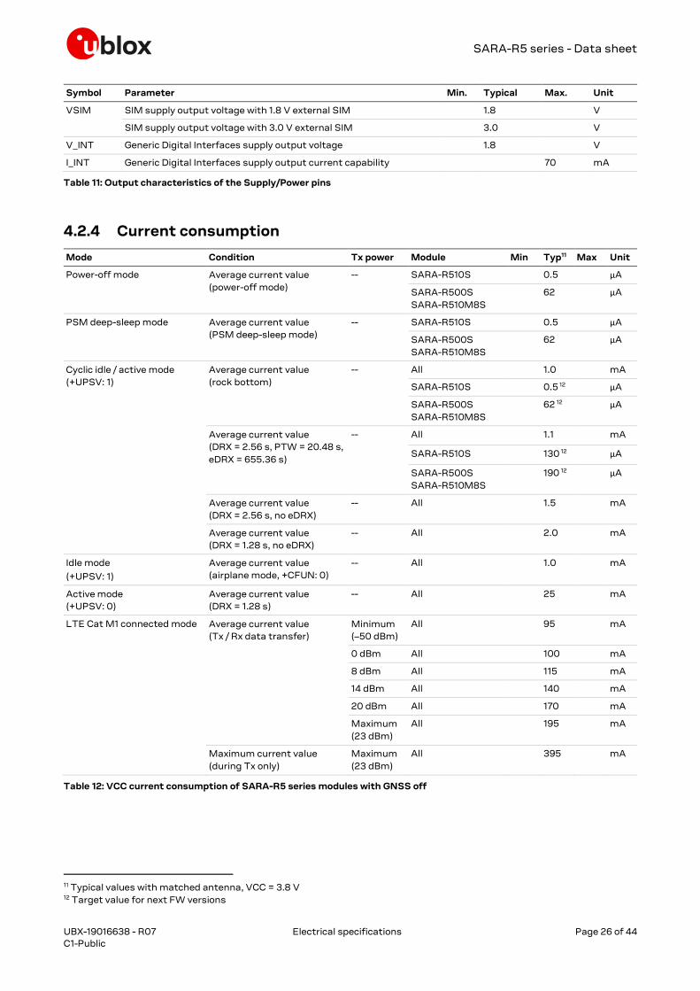
SARA-R5 series - Data sheet
UBX-19016638 - R07 Electrical specifications Page 26 of 44
C1-Public
Symbol Parameter Min. Typical Max. Unit
VSIM SIM supply output voltage with 1.8 V external SIM 1.8 V
SIM supply output voltage with 3.0 V external SIM 3.0 V
V_INT Generic Digital Interfaces supply output voltage 1.8 V
I_INT Generic Digital Interfaces supply output current capability 70 mA
Table 11: Output characteristics of the Supply/Power pins
4.2.4 Current consumption
Mode Condition Tx power Module Min Typ11 Max Unit
Power-off mode Average current value
(power-off mode)
-- SARA-R510S 0.5 µA
SARA-R500S
SARA-R510M8S
62 µA
PSM deep-sleep mode Average current value
(PSM deep-sleep mode)
-- SARA-R510S 0.5 µA
SARA-R500S
SARA-R510M8S
62 µA
Cyclic idle / active mode
(+UPSV: 1)
Average current value
(rock bottom)
-- All 1.0 mA
SARA-R510S 0.5 12 µA
SARA-R500S
SARA-R510M8S
62 12 µA
Average current value
(DRX = 2.56 s, PTW = 20.48 s,
eDRX = 655.36 s)
-- All 1.1 mA
SARA-R510S 130 12 µA
SARA-R500S
SARA-R510M8S
190 12 µA
Average current value
(DRX = 2.56 s, no eDRX)
-- All 1.5 mA
Average current value
(DRX = 1.28 s, no eDRX)
-- All 2.0 mA
Idle mode
(+UPSV: 1)
Average current value
(airplane mode, +CFUN: 0)
-- All 1.0 mA
Active mode
(+UPSV: 0)
Average current value
(DRX = 1.28 s)
-- All 25 mA
LTE Cat M1 connected mode Average current value
(Tx / Rx data transfer)
Minimum
(–50 dBm)
All 95 mA
0 dBm All 100 mA
8 dBm All 115 mA
14 dBm All 140 mA
20 dBm All 170 mA
Maximum
(23 dBm)
All 195 mA
Maximum current value
(during Tx only)
Maximum
(23 dBm)
All 395 mA
Table 12: VCC current consumption of SARA-R5 series modules with GNSS off
11 Typical values with matched antenna, VCC = 3.8 V 12 Target value for next FW versions

SARA-R5 series - Data sheet
UBX-19016638 - R07 Electrical specifications Page 27 of 44
C1-Public
Mode / Condition Min Typ13 Max Unit
Average current value with power saving enabled (+UPSV=1),
UBX-R5 in PSM, UBX-M8 in cyclic tracking mode with 1 s update period (GPS)
15 mA
Average current value with power saving enabled (+UPSV=1),
UBX-R5 in PSM, UBX-M8 in cyclic tracking mode with 1 s update period (GPS & GLONASS)
16 mA
Average current value with power saving enabled (+UPSV=1),
UBX-R5 in PSM, UBX-M8 in continuous tracking mode (GPS & GLONASS)
43 mA
Average current value with power saving enabled (+UPSV=1),
UBX-R5 in DRX = 1.28 s, UBX-M8 in cyclic tracking mode with 1 s update period (GPS)
16 mA
Average current value with power saving enabled (+UPSV=1),
UBX-R5 in DRX = 1.28 s, UBX-M8 in cyclic tracking mode with 1 s update period (GPS & GLONASS)
17 mA
Average current value with power saving enabled (+UPSV=1),
UBX-R5 in DRX = 1.28 s, UBX-M8 in continuous tracking mode (GPS & GLONASS)
44 mA
Average current value with power saving disabled (+UPSV=0),
UBX-R5 in DRX = 1.28 s, UBX-M8 in continuous tracking mode (GPS & GLONASS)
67 mA
Average current value with power saving disabled (+UPSV=0),
UBX-R5 in DRX = 1.28 s, UBX-M8 in acquisition mode (GPS & GLONASS)
72 mA
Peak current value with power saving disabled (+UPSV=0),
UBX-R5 in DRX = 1.28 s, UBX-M8 in acquisition mode (GPS & GLONASS)
100 mA
Table 13: Indicative VCC current consumption of the SARA-R510M8S module with GNSS on
4.2.5 GNSS characteristics
Parameter Condition Value
Receiver type 72-channel u-blox M8 engine
GPS L1C/A, SBAS L1C/A, QZSS L1C/A, QZSS L1-SAIF,
GLONASS L1OF, BeiDou B1I, Galileo E1B/C
Operational limits14 Dynamics ≤ 4 g
Altitude 50’000 m
Velocity 500 m/s
Velocity accuracy15 0.05 m/s
Heading accuracy15 0.3 degrees
GNSS GPS & GLONASS GPS GLONASS BeiDou Galileo
Horizontal position accuracy16 2.5 m 2.5 m 4 m 3 m 3 m
Max navigation update rate 10 Hz 18 Hz 18 Hz 18 Hz 18 Hz
Time-To-First-Fix17 Cold start 26 s 29 s 30 s 34 s 45 s
Aided starts18 2 s 2 s 2 s 3 s 7 s
Sensitivity Tracking & Navigation -167 dBm -166 dBm -166 dBm -160 dBm -159 dBm
Reacquisition -160 dBm -160 dBm -156 dBm -157 dBm -153 dBm
Cold start -148 dBm -148 dBm -145 dBm -143 dBm -138 dBm
Table 14: GNSS characteristics and performance of the SARA-R510M8S module
13 Typical values with matched antenna, VCC = 3.8 V 14 Assuming Airborne < 4 g platform 15 50% @ 30 m/s 16 CEP, 50%, 24 hours static, -130 dBm, > 6 SVs 17 All satellites at -130 dBm, except Galileo at -127 dBm 18 Dependent on aiding data connection speed and latency 19 Not supported in LTE category M1

SARA-R5 series - Data sheet
UBX-19016638 - R07 Electrical specifications Page 28 of 44
C1-Public
4.2.6 LTE RF characteristics
The LTE Cat M1 / NB2 bands supported by SARA-R5 series modules are defined in Table 2, while the
following Table 15 describes the frequency ranges for each LTE band as per 3GPP TS 36.521-1 [7].
Parameter Min. Max. Unit Remarks
Frequency range
FDD band 71 (600 MHz) 19
Uplink 663 698 MHz Module transmit
Downlink 617 652 MHz Module receive
Frequency range
FDD band 12 (700 MHz)
Uplink 699 716 MHz Module transmit
Downlink 729 746 MHz Module receive
Frequency range
FDD band 28 (700 MHz)
Uplink 703 748 MHz Module transmit
Downlink 758 803 MHz Module receive
Frequency range
FDD band 85 (700 MHz) 19
Uplink 698 716 MHz Module transmit
Downlink 728 746 MHz Module receive
Frequency range
FDD band 13 (750 MHz)
Uplink 777 787 MHz Module transmit
Downlink 746 756 MHz Module receive
Frequency range
FDD band 20 (800 MHz)
Uplink 832 862 MHz Module transmit
Downlink 791 821 MHz Module receive
Frequency range
FDD band 26 (850 MHz)
Uplink 814 849 MHz Module transmit
Downlink 859 894 MHz Module receive
Frequency range
FDD band 18 (850 MHz)
Uplink 815 830 MHz Module transmit
Downlink 860 875 MHz Module receive
Frequency range
FDD band 5 (850 MHz)
Uplink 824 849 MHz Module transmit
Downlink 869 894 MHz Module receive
Frequency range
FDD band 19 (850 MHz)
Uplink 830 845 MHz Module transmit
Downlink 875 890 MHz Module receive
Frequency range
FDD band 8 (900 MHz)
Uplink 880 915 MHz Module transmit
Downlink 925 960 MHz Module receive
Frequency range
FDD band 4 (1700 MHz)
Uplink 1710 1755 MHz Module transmit
Downlink 2110 2155 MHz Module receive
Frequency range
FDD band 66 (1700 MHz) 19
Uplink 1710 1780 MHz Module transmit
Downlink 2110 2200 MHz Module receive
Frequency range
FDD band 3 (1800 MHz)
Uplink 1710 1785 MHz Module transmit
Downlink 1805 1880 MHz Module receive
Frequency range
FDD band 2 (1900 MHz)
Uplink 1850 1910 MHz Module transmit
Downlink 1930 1990 MHz Module receive
Frequency range
FDD band 25 (1900 MHz) 20
Uplink 1850 1915 MHz Module transmit
Downlink 1930 1995 MHz Module receive
Frequency range
FDD band 1 (2100 MHz)
Uplink 1920 1980 MHz Module transmit
Downlink 2110 2170 MHz Module receive
Table 15: LTE operating RF frequency bands
SARA-R5 series modules include a UE Power Class 3 LTE Cat M1 / NB2 transmitter (see Table 2) and
an LTE receiver, with output power and characteristics according to 3GPP TS 36.521-1 [7].
The “00” products version of the SARA-R5 series modules do not support LTE NB-IoT.
19 Not supported in LTE category M1 20 Not supported in LTE category NB2

SARA-R5 series - Data sheet
UBX-19016638 - R07 Electrical specifications Page 29 of 44
C1-Public
SARA-R5 series modules LTE receiver characteristics are compliant to 3GPP TS 36.521-1 [7], with LTE
conducted receiver sensitivity performance described in Table 16.
Parameter Min. Typical Max. Unit Remarks
Receiver input sensitivity
Band 12 (700 MHz)
–110.5 dBm Without repetitions
Receiver input sensitivity
Band 28 (700 MHz)
–110.5 dBm Without repetitions
Receiver input sensitivity
Band 13 (750 MHz)
–110.5 dBm Without repetitions
Receiver input sensitivity
Band 20 (800 MHz)
–110.5 dBm Without repetitions
Receiver input sensitivity
Band 26 (850 MHz)
–110.0 dBm Without repetitions
Receiver input sensitivity
Band 18 (850 MHz)
–110.0 dBm Without repetitions
Receiver input sensitivity
Band 5 (850 MHz)
–110.0 dBm Without repetitions
Receiver input sensitivity
Band 19 (850 MHz)
–110.0 dBm Without repetitions
Receiver input sensitivity
Band 8 (900 MHz)
–109.5 dBm Without repetitions
Receiver input sensitivity
Band 4 (1700 MHz)
–109.0 dBm Without repetitions
Receiver input sensitivity
Band 3 (1800 MHz)
–109.0 dBm Without repetitions
Receiver input sensitivity
Band 2 (1900 MHz)
–109.0 dBm Without repetitions
Receiver input sensitivity
Band 25 (1900 MHz)
–109.0 dBm Without repetitions
Receiver input sensitivity
Band 1 (2100 MHz)
–109.0 dBm Without repetitions
Condition: 50 source, throughput > 95%, QPSK modulation, other settings as per clause 7.3EA of 3GPP TS 36.521-1 [7]
Table 16: LTE Cat M1 receiver sensitivity performance
4.2.7 ANT_DET pin
Pin Name Parameter Min. Typ. Max. Unit Remarks
ANT_DET Output DC current pulse value 3 µA
Output DC current pulse time length 20 ms
Table 17: ANT_DET pin characteristics
4.2.8 Time pulse
Parameter Specification Unit
Accuracy of time pulse / time stamp GNSS source 21 RMS
99%
50
100
ns
ns
LTE source RMS
99%
500
1
ns
µs
Frequency of time pulse 1 Hz
Table 18: Time pulse / time stamp characteristics
21 Time pulse / time stamp is always generated by the UBX-R5 cellular chipset after the process of the GNSS time pulse signal.

SARA-R5 series - Data sheet
UBX-19016638 - R07 Electrical specifications Page 30 of 44
C1-Public
4.2.9 PWR_ON pin
Parameter Module Min. Typical Max. Unit Remarks
Low-level input All -0.3 0.3 V
Pull-up resistance All 10 k Integrated pull-up to internal rail
Low-level input current All -300 µA
PWR_ON low time SARA-R510S 1 2 s Low time to trigger module switch-on from
power-off mode
1 2 s Low time to trigger module wake-up from PSM
deep-sleep
SARA-R500S
SARA-R510M8S
0.1 2 s Low time to trigger module switch-on from
power-off mode
0.1 2 s Low time to trigger module wake-up from PSM
deep-sleep
Table 19: PWR_ON pin characteristics
The PWR_ON and RESET_N input lines have to be driven as described in Figure 5 to perform an abrupt
emergency hardware shutdown of the SARA-R5 series modules:
• First, PWR_ON line has to be set to the LOW level
• Then, RESET_N line has to be set to the LOW level, keeping the PWR_ON line set to the LOW level
• Then, after at least 23 s (minimum) since the PWR_ON line has been set to the LOW level, the
PWR_ON line has to be released to the HIGH level, keeping the RESET_N line set to the LOW level
• Then, after at least 1.5 s (minimum) since the PWR_ON line has been released to the HIGH level,
the RESET_N line has to be released to the HIGH level
1.5 s < T
Time
RESET_N
23 s < T
PWR_ON
Figure 5: PWR_ON and RESET_N lines waveforms timings to perform an abrupt emergency hardware shutdown
4.2.10 RESET_N pin
Parameter Min. Typical Max. Unit Remarks
Internal supply 1.8 Digital I/O Interfaces supply (V_INT)
Low-level input -0.3 0.5 V
Low-level input current -18 -32 -56 µA
RESET_N low time 100 ms Low time to trigger module reset / reboot
Table 20: RESET_N pin characteristics
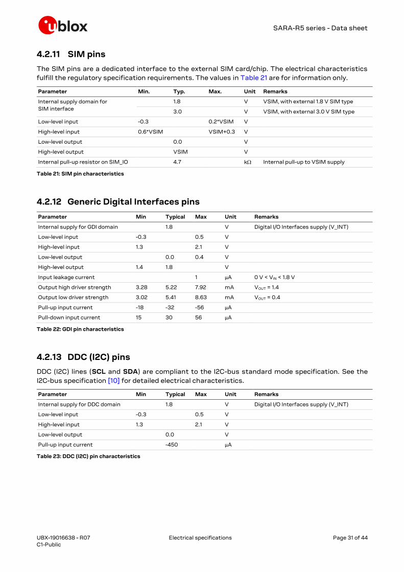
SARA-R5 series - Data sheet
UBX-19016638 - R07 Electrical specifications Page 31 of 44
C1-Public
4.2.11 SIM pins
The SIM pins are a dedicated interface to the external SIM card/chip. The electrical characteristics
fulfill the regulatory specification requirements. The values in Table 21 are for information only.
Parameter Min. Typ. Max. Unit Remarks
Internal supply domain for
SIM interface
1.8 V VSIM, with external 1.8 V SIM type
3.0 V VSIM, with external 3.0 V SIM type
Low-level input -0.3 0.2*VSIM V
High-level input 0.6*VSIM VSIM+0.3 V
Low-level output 0.0 V
High-level output VSIM V
Internal pull-up resistor on SIM_IO 4.7 k Internal pull-up to VSIM supply
Table 21: SIM pin characteristics
4.2.12 Generic Digital Interfaces pins
Parameter Min Typical Max Unit Remarks
Internal supply for GDI domain 1.8 V Digital I/O Interfaces supply (V_INT)
Low-level input -0.3 0.5 V
High-level input 1.3 2.1 V
Low-level output 0.0 0.4 V
High-level output 1.4 1.8 V
Input leakage current 1 µA 0 V < VIN < 1.8 V
Output high driver strength 3.28 5.22 7.92 mA VOUT = 1.4
Output low driver strength 3.02 5.41 8.63 mA VOUT = 0.4
Pull-up input current -18 -32 -56 µA
Pull-down input current 15 30 56 µA
Table 22: GDI pin characteristics
4.2.13 DDC (I2C) pins
DDC (I2C) lines (SCL and SDA) are compliant to the I2C-bus standard mode specification. See the
I2C-bus specification [10] for detailed electrical characteristics.
Parameter Min Typical Max Unit Remarks
Internal supply for DDC domain 1.8 V Digital I/O Interfaces supply (V_INT)
Low-level input -0.3 0.5 V
High-level input 1.3 2.1 V
Low-level output 0.0 V
Pull-up input current -450 µA
Table 23: DDC (I2C) pin characteristics

SARA-R5 series - Data sheet
UBX-19016638 - R07 Electrical specifications Page 32 of 44
C1-Public
4.2.14 USB pins
USB data lines (USB_D+ / USB_D–) are compliant with the USB 2.0 high-speed specification. See the
Universal Serial Bus specification revision 2.0 [9] for detailed electrical characteristics. The values in
Table 24 related to USB 2.0 high-speed physical layer specifications are for information only.
Parameter Min. Typical Max. Unit Remarks
VUSB_DET pin, High-level input 4.40 5.00 5.25 V
High-speed squelch detection threshold
(input differential signal amplitude)
100 150 mV
High speed disconnect detection threshold
(input differential signal amplitude)
525 625 mV
High-speed data signaling input
common mode voltage range
–50 500 mV
High-speed idle output level –10 10 mV
High-speed data signaling output high level 360 440 mV
High-speed data signaling output low level –10 10 mV
Chirp J level (output differential voltage) 700 1100 mV
Chirp K level (output differential voltage) –900 –500 mV
Table 24: USB pins characteristics
4.2.15 Smart temperature supervisor
Warningarea
t-1 t+1 t+2t-2
Valid temperature range
Safearea
Dangerousarea
Dangerousarea
Warningarea
Figure 6: Temperature range and limits
Symbol Parameter Temperature
t-2 Low temperature shutdown –40 °C
t-1 Low temperature warning –30 °C
t+1 High temperature warning +77 °C
t+2 High temperature shutdown +97 °C
Table 25: Thresholds definition for the “Smart temperature supervisor” feature on the SARA-R5 series modules
The sensor measures the board temperature inside the shield, which can differ from the ambient
temperature.
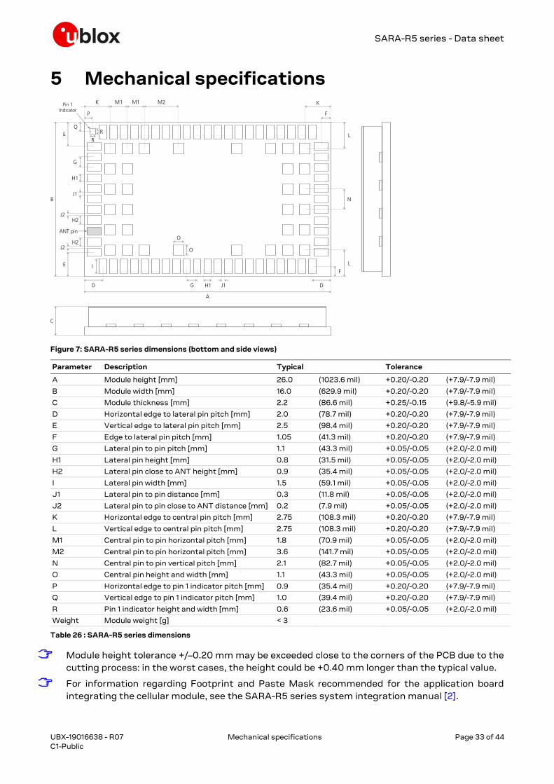
SARA-R5 series - Data sheet
UBX-19016638 - R07 Mechanical specifications Page 33 of 44
C1-Public
5 Mechanical specifications
C
R
R
P
Q
K M1 M1 M2
E
G
H1
J1
H2J2
J2H2
E
ANT pin
B
Pin 1
Indicator
K
G H1 J1
A
D D
O
O
L
N
LI
F
F
Figure 7: SARA-R5 series dimensions (bottom and side views)
Parameter Description Typical Tolerance
A Module height [mm] 26.0 (1023.6 mil) +0.20/-0.20 (+7.9/-7.9 mil)
B Module width [mm] 16.0 (629.9 mil) +0.20/-0.20 (+7.9/-7.9 mil)
C Module thickness [mm] 2.2 (86.6 mil) +0.25/-0.15 (+9.8/-5.9 mil)
D Horizontal edge to lateral pin pitch [mm] 2.0 (78.7 mil) +0.20/-0.20 (+7.9/-7.9 mil)
E Vertical edge to lateral pin pitch [mm] 2.5 (98.4 mil) +0.20/-0.20 (+7.9/-7.9 mil)
F Edge to lateral pin pitch [mm] 1.05 (41.3 mil) +0.20/-0.20 (+7.9/-7.9 mil)
G Lateral pin to pin pitch [mm] 1.1 (43.3 mil) +0.05/-0.05 (+2.0/-2.0 mil)
H1 Lateral pin height [mm] 0.8 (31.5 mil) +0.05/-0.05 (+2.0/-2.0 mil)
H2 Lateral pin close to ANT height [mm] 0.9 (35.4 mil) +0.05/-0.05 (+2.0/-2.0 mil)
I Lateral pin width [mm] 1.5 (59.1 mil) +0.05/-0.05 (+2.0/-2.0 mil)
J1 Lateral pin to pin distance [mm] 0.3 (11.8 mil) +0.05/-0.05 (+2.0/-2.0 mil)
J2 Lateral pin to pin close to ANT distance [mm] 0.2 (7.9 mil) +0.05/-0.05 (+2.0/-2.0 mil)
K Horizontal edge to central pin pitch [mm] 2.75 (108.3 mil) +0.20/-0.20 (+7.9/-7.9 mil)
L Vertical edge to central pin pitch [mm] 2.75 (108.3 mil) +0.20/-0.20 (+7.9/-7.9 mil)
M1 Central pin to pin horizontal pitch [mm] 1.8 (70.9 mil) +0.05/-0.05 (+2.0/-2.0 mil)
M2 Central pin to pin horizontal pitch [mm] 3.6 (141.7 mil) +0.05/-0.05 (+2.0/-2.0 mil)
N Central pin to pin vertical pitch [mm] 2.1 (82.7 mil) +0.05/-0.05 (+2.0/-2.0 mil)
O Central pin height and width [mm] 1.1 (43.3 mil) +0.05/-0.05 (+2.0/-2.0 mil)
P Horizontal edge to pin 1 indicator pitch [mm] 0.9 (35.4 mil) +0.20/-0.20 (+7.9/-7.9 mil)
Q Vertical edge to pin 1 indicator pitch [mm] 1.0 (39.4 mil) +0.20/-0.20 (+7.9/-7.9 mil)
R Pin 1 indicator height and width [mm] 0.6 (23.6 mil) +0.05/-0.05 (+2.0/-2.0 mil)
Weight Module weight [g] < 3
Table 26 : SARA-R5 series dimensions
Module height tolerance +/–0.20 mm may be exceeded close to the corners of the PCB due to the
cutting process: in the worst cases, the height could be +0.40 mm longer than the typical value.
For information regarding Footprint and Paste Mask recommended for the application board
integrating the cellular module, see the SARA-R5 series system integration manual [2].
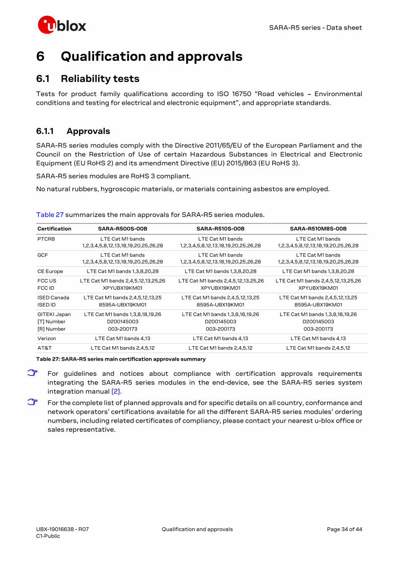
SARA-R5 series - Data sheet
UBX-19016638 - R07 Qualification and approvals Page 34 of 44
C1-Public
6 Qualification and approvals
6.1 Reliability tests
Tests for product family qualifications according to ISO 16750 “Road vehicles – Environmental
conditions and testing for electrical and electronic equipment”, and appropriate standards.
6.1.1 Approvals
SARA-R5 series modules comply with the Directive 2011/65/EU of the European Parliament and the
Council on the Restriction of Use of certain Hazardous Substances in Electrical and Electronic
Equipment (EU RoHS 2) and its amendment Directive (EU) 2015/863 (EU RoHS 3).
SARA-R5 series modules are RoHS 3 compliant.
No natural rubbers, hygroscopic materials, or materials containing asbestos are employed.
Table 27 summarizes the main approvals for SARA-R5 series modules.
Certification SARA-R500S-00B SARA-R510S-00B SARA-R510M8S-00B
PTCRB LTE Cat M1 bands
1,2,3,4,5,8,12,13,18,19,20,25,26,28
LTE Cat M1 bands
1,2,3,4,5,8,12,13,18,19,20,25,26,28
LTE Cat M1 bands
1,2,3,4,5,8,12,13,18,19,20,25,26,28
GCF LTE Cat M1 bands
1,2,3,4,5,8,12,13,18,19,20,25,26,28
LTE Cat M1 bands
1,2,3,4,5,8,12,13,18,19,20,25,26,28
LTE Cat M1 bands
1,2,3,4,5,8,12,13,18,19,20,25,26,28
CE Europe LTE Cat M1 bands 1,3,8,20,28 LTE Cat M1 bands 1,3,8,20,28 LTE Cat M1 bands 1,3,8,20,28
FCC US
FCC ID
LTE Cat M1 bands 2,4,5,12,13,25,26
XPYUBX19KM01
LTE Cat M1 bands 2,4,5,12,13,25,26
XPYUBX19KM01
LTE Cat M1 bands 2,4,5,12,13,25,26
XPYUBX19KM01
ISED Canada
ISED ID
LTE Cat M1 bands 2,4,5,12,13,25
8595A-UBX19KM01
LTE Cat M1 bands 2,4,5,12,13,25
8595A-UBX19KM01
LTE Cat M1 bands 2,4,5,12,13,25
8595A-UBX19KM01
GITEKI Japan
[T] Number
[R] Number
LTE Cat M1 bands 1,3,8,18,19,26
D200145003
003-200173
LTE Cat M1 bands 1,3,8,18,19,26
D200145003
003-200173
LTE Cat M1 bands 1,3,8,18,19,26
D200145003
003-200173
Verizon LTE Cat M1 bands 4,13 LTE Cat M1 bands 4,13 LTE Cat M1 bands 4,13
AT&T LTE Cat M1 bands 2,4,5,12 LTE Cat M1 bands 2,4,5,12 LTE Cat M1 bands 2,4,5,12
Table 27: SARA-R5 series main certification approvals summary
For guidelines and notices about compliance with certification approvals requirements
integrating the SARA-R5 series modules in the end-device, see the SARA-R5 series system
integration manual [2].
For the complete list of planned approvals and for specific details on all country, conformance and
network operators’ certifications available for all the different SARA-R5 series modules’ ordering
numbers, including related certificates of compliancy, please contact your nearest u-blox office or
sales representative.

SARA-R5 series - Data sheet
UBX-19016638 - R07 Product handling & soldering Page 35 of 44
C1-Public
7 Product handling & soldering
7.1 Packaging
SARA-R5 series modules are delivered as hermetically sealed, reeled tapes to enable efficient
production, production lot set-up and tear-down. For more information about packaging, see the
u-blox package information user guide [3].
7.1.1 Reels
SARA-R5 series modules are deliverable in quantities of 250 pieces on a reel. The modules are
delivered using reel type B2 described in Figure 8 and in the u-blox package information user guide [3].
Figure 8: SARA-R5 series modules reel
Parameter Specification
Reel type B2
Delivery quantity 250
Table 28: Reel information for SARA-R5 series modules
Quantities of less than 250 pieces are also available. Contact u-blox for more information.

SARA-R5 series - Data sheet
UBX-19016638 - R07 Product handling & soldering Page 36 of 44
C1-Public
7.1.2 Tapes
Figure 9 shows the position and the orientation of SARA-R5 series modules as they are delivered on
the tape, while Figure 10 and Table 29 specify the dimensions of the tape.
Pin 1Sprocket hole
Feed direction
Figure 9: Orientation of SARA-R5 series modules on tape
Figure 10: SARA-R5 series modules tape
Parameter Typical value Tolerance Unit
A0 16.8 0.2 mm
B0 26.8 0.2 mm
K0 3.2 0.2 mm
Table 29 : SARA-R5 series tape dimensions (mm)
10 sprocket hole pitch cumulative tolerance ± 0.2 mm.
Pocket position relative to sprocket hole is measured as true position of pocket, not pocket hole.
A0 and B0 are calculated on a plane at a distance “R” above the bottom of the pocket.

SARA-R5 series - Data sheet
UBX-19016638 - R07 Product handling & soldering Page 37 of 44
C1-Public
7.2 Moisture sensitivity levels
SARA-R5 series modules are moisture sensitive devices (MSD) in accordance to the IPC/JEDEC
specification.
The Moisture Sensitivity Level (MSL) relates to the packaging and handling precautions required.
SARA-R5 series modules are rated at MSL level 4. For more information regarding moisture
sensitivity levels, labeling, storage and drying, see the u-blox package information user guide [3].
For the MSL standard, see IPC/JEDEC J-STD-020 (can be downloaded from www.jedec.org).
7.3 Reflow soldering
Reflow profiles are to be selected according to u-blox recommendations (see the SARA-R5 series
system integration manual [2]).
Failure to observe these recommendations can result in severe damage to the device!
7.4 ESD precautions
SARA-R5 series modules contain highly sensitive electronic circuitry and are Electrostatic
Sensitive Devices (ESD). Handling SARA-R5 series modules without proper ESD protection may
destroy or damage them permanently.
SARA-R5 series modules are Electrostatic Sensitive Devices (EDS) and require special ESD
precautions typically applied to ESD sensitive components.
Table 7 details the maximum ESD ratings of the SARA-R5 series modules.
Proper ESD handling and packaging procedures must be applied throughout the processing, handling
and operation of any application that incorporates SARA-R5 series modules.
ESD precautions should be appropriately implemented on the application board where the module is
mounted, as described in the SARA-R5 series system integration manual [2].
Failure to observe these precautions can result in severe damage to the device!

SARA-R5 series - Data sheet
UBX-19016638 - R07 Labeling and ordering information Page 38 of 44
C1-Public
8 Labeling and ordering information
8.1 Product labeling
The labels of SARA-R5 series modules include important product information as described in this
section. Figure 11 illustrates the label of the SARA-R5 series modules, and includes: u-blox logo,
production lot, Pb-free marking, product type number, IMEI number, certification information, and
production country.
SARA-xxxxx
xxB-xx
FCC ID: XPYUBX19KM01
IC: 8595A-UBX19KM01
Figure 11: SARA-R5 series module label
8.2 Explanation of codes
Three different product code formats are used. The Product Name is used in documentation such as
this data sheet and identifies all the u-blox products, independent of packaging and quality grade. The
Ordering Code includes options and quality, while the Type Number includes the hardware and
firmware versions. Table 30 details these 3 different formats:
Format Structure
Product Name PPPP-TGVV(HH)(F)
Ordering Code PPPP-TGVV(HH)(F)-MMQ
Type Number PPPP-TGVV(HH)(F)-MMQ-XX
Table 30: Product code formats
Table 31 explains the parts of the product code.
Code Meaning Example
PPPP Form factor SARA
TG Platform (Technology and Generation)
• Dominant technology: G = GSM, U = HSUPA, C = CDMA 1xRTT, N = NB-IoT (LTE Cat NB1),
R = LTE low data rate (Cat 1 and Cat M1), L = LTE high data rate (Cat 3 and above)
• Generation: 1…9
R5
VV Variant function set based on the same platform: 00…99 10
(HH) GNSS generation (optional): M8 = u-blox M8, M9 = u-blox M9, … M8
(F) Additional features (optional): S = secure cloud, … S
MM Major product version: 00…99 00
Q Product grade: C = standard, B = professional, A = automotive B
XX Minor product version: 00…99 Default value is 00
Table 31: Part identification code

SARA-R5 series - Data sheet
UBX-19016638 - R07 Labeling and ordering information Page 39 of 44
C1-Public
8.3 Ordering information
Ordering No. Product
SARA-R500S-00B Secure cloud LTE Cat M1 module for multi-region use.
26.0 x 16.0 mm, 250 pieces/reel
SARA-R510S-00B Secure cloud LTE Cat M1 module for multi-region use.
Designed for extremely low current consumption in deep-sleep power saving mode (PSM).
26.0 x 16.0 mm, 250 pieces/reel
SARA-R510M8S-00B Secure cloud LTE Cat M1 module for multi-region use.
Designed with integrated u-blox M8 GNSS receiver, concurrently available with LTE network access.
26.0 x 16.0 mm, 250 pieces/reel
Table 32: Product ordering codes

SARA-R5 series - Data sheet
UBX-19016638 - R07 Appendix Page 40 of 44
C1-Public
Appendix
A Glossary Abbreviation Definition
3GPP 3rd Generation Partnership Project
ADC Analog to Digital Converter
AT AT Command Interpreter Software Subsystem, or attention
BB Baseband
BeiDou Chinese satellite navigation system
BER Bit Error Rate
Cat Category
CBS Cell Broadcast Service
CCC China Compulsory Certificate
CE Coverage Enhancement
CE European Conformity
CEP Circular Error Probable
CLK Clock
CIoT Cellular Internet of Things
CMOS Complementary Metal-Oxide-Semiconductor
CoAP Constrained Application Protocol
CS Chip Select
CTS Clear To Send
DC Direct Current
DCD Data Carrier Detect
DCS Digital Cellular System
DDC Display Data Channel
DL Down Link (Reception)
DRX Discontinuous Reception
DSR Data Set Ready
DTE Data Terminal Equipment
DTLS Datagram Transport Layer Security
DTR Data Terminal Ready
DUN Dial-Up Networking
E-CID Enhanced Cell Identity
eDRX Extended Discontinuous Reception
EPS Evolved Packet System
ESD Electrostatic Discharge
E-UTRA Evolved Universal Terrestrial Radio Access
FCC Federal Communications Commission United States
FDD Frequency Division Duplex
FOAT Firmware (update) Over AT commands
FOTA Firmware (update) Over-The-Air
FTP File Transfer Protocol
FW Firmware
SARA-R5 series - Data sheet
UBX-19016638 - R07 Appendix Page 41 of 44
C1-Public
Abbreviation Definition
Galileo European satellite navigation system
GCF Global Certification Forum
GDI Generic Digital Interface
GLONASS Russian satellite navigation system
GND Ground
GNSS Global Navigation Satellite System
GPIO General Purpose Input/Output
GPS Global Positioning System
HARQ Hybrid Automatic Repeat Request
HDLC High-level Data Link Control
HTTP HyperText Transfer Protocol
HW Hardware
IEC International Electrotechnical Commission
IFT Federal Telecommunications Institute Mexico
I2C Inter-Integrated Circuit
I2S Inter-IC Sound
I/O Input/Output
IMEI International Mobile Equipment Identity
IP Internet Protocol
ISED Innovation, Science and Economic Development Canada
ISO International Organization for Standardization
ITU International Telecommunications Union
LGA Land Grid Array
LNA Low Noise Amplifier
LPWA Low Power Wide Area
LTE Long-Term Evolution
LTE-M Long-Term Evolution – enhanced Machine Type Communication
LwM2M Lightweight Machine-to-Machine protocol
M2M Machine to Machine
MISO Multiple Input Single Output
MOSI Master Output Slave Input
MQTT Message Queuing Telemetry Transport
MQTT-SN Message Queuing Telemetry Transport for Sensor Networks
MSD Moisture Sensitive Device
MSL Moisture Sensitivity Level
MUX Multiplexer
N/A Not Applicable
NB-IoT Narrowband Internet of Things
NCC National Communications Commission Taiwan
PA Power Amplifier
PCB Printed Circuit Board
PCN Product Change Notification / Sample Delivery Note / Information Note
PMU Power Management Unit
POS Power On Signal
PPS Pulse Per Second
PSM Power Saving Mode

SARA-R5 series - Data sheet
UBX-19016638 - R07 Appendix Page 42 of 44
C1-Public
Abbreviation Definition
PTCRB PCS Type Certification Review Board
PUCCH Physical Uplink Control Channel
QPSK Quadrature Phase Shift Keying modulation
QZSS Quasi-Zenith Satellite System
RACH Random Access Channel
RAM Random Access Memory
RAT Radio Access Technology
RF Radio Frequency
RI Ring Indicator
RIL Radio Interface Layer
RRC Radio Resource Control
RTC Real Time Clock
RTS Request To Send
Rx Reception
SAW Surface Acoustic Wave
SBAS Satellite-Based Augmentation System
SCL Serial Clock
SDA Serial Data
SDIO Secure Digital Input Output
SIM Subscriber Identity Module
SMS Short Message Service
SPG Standard Precision GNSS
SPI Serial Peripheral Interface
SSL Secure Socket Layer
TBS Transport Block Size
TCP Transmission Control Protocol
TDD Time Division Duplex
TLS Transport Layer Security
TS Technical Specification
Tx Transmission
TXD Transmit Data
UART Universal Asynchronous Receiver/Transmitter
uCSP u-blox Common Services Platform
UDP User Datagram Protocol
UE User Equipment
uFOTA u-blox Firmware (update) Over-The-Air
UL Uplink (Transmission)
URC Unsolicited Result Code
USB Universal Serial Bus
VoLTE Voice over LTE
VSWR Voltage Standing Wave Ratio
WA Word Alignment
Table 33: Explanation of the abbreviations and terms used

SARA-R5 series - Data sheet
UBX-19016638 - R07 Related documents Page 43 of 44
C1-Public
Related documents [1] u-blox SARA-R5 series AT commands manual, UBX-19047455
[2] u-blox SARA-R5 series system integration manual, UBX-19041356
[3] u-blox package information user guide, UBX-14001652
[4] 3GPP TS 27.007 - AT command set for User Equipment (UE)
[5] 3GPP TS 27.005 - Use of Data Terminal Equipment - Data Circuit terminating Equipment
(DTE - DCE) interface for Short Message Service (SMS) and Cell Broadcast Service (CBS)
[6] 3GPP TS 27.010 - Terminal Equipment to User Equipment (TE-UE) multiplexer protocol
[7] 3GPP TS 36.521-1 - Evolved Universal Terrestrial Radio Access; User Equipment conformance
specification; Radio transmission and reception; Part 1: Conformance Testing
[8] ITU-T Recommendation V24 - List of definitions for interchange circuits between Data
Terminal Equipment (DTE) and Data Connection Equipment (DCE)
[9] Universal Serial Bus Revision 2.0 specification, https://www.usb.org/
[10] I2C-bus specification and user manual - NXP semiconductors,
https://www.nxp.com/docs/en/user-guide/UM10204.pdf
[11] RFC 7252 - Constrained Application Protocol (CoAP)
For regular updates to u-blox documentation and to receive product change notifications, register
on our homepage (www.u-blox.com).
Revision history Revision Date Name Comments
R01 02-Aug-2019 fvid / sses Initial release
R02 17-Oct-2019 fvid Updated GPIO section. Updated RESET_N and generic digital interfaces
electrical specifications. Updated normal operating temperature.
R03 07-Nov-2019 sses Updated document products applicability.
Updated Power-on, Power-off and Reset sections. Updated GPIO section.
Updated pin 2 name and function. Updated absolute maximum ratings.
Minor other corrections and clarifications.
R04 20-Dec-2019 fvid / sses Added current consumption and LTE Cat M1 receiver sensitivity figures.
Updated UART section. Updated GPIO section.
Updated DDC (I2C) electrical specifications.
Update the module thickness, Minor other corrections and clarifications.
R05 06-Mar-2020 fvid / sses Extended the document applicability to SARA-R500S-00B.
NB-IoT radio access technology not supported by "00" products version.
GPIO, Power-on, Power-off, Reset sections and characteristics updated.
Added some current consumption figures.
Other minor corrections and clarifications.
R06 15-Jul-2020 sses / fvid Updated document products status.
Updated GPIO section and PWR_ON timings.
Added some current consumption figures, and GNSS performance figures.
Other minor corrections and clarifications.
R07 02-Oct-2020 sses / fvid Updated document products status.
Updated Supported features section. Updated Power-on, Power-off and
Reset sections. Added GITEKI certification.
Updated electrical specifications: added thermal parameters; updated
current consumption table and added target values; added ANT_DET
characteristics; added time pulse characteristics; updated PWR_ON pin
characteristics; added “Smart temperature supervisor” characteristics.
Other minor corrections and clarifications.

SARA-R5 series - Data sheet
UBX-19016638 - R07 Contact Page 44 of 44
C1-Public
Contact For complete contact information, visit us at www.u-blox.com.
u-blox Offices
North, Central and South America
u-blox America, Inc.
Phone: +1 703 483 3180
E-mail: [email protected]
Regional Office West Coast:
Phone: +1 408 573 3640
E-mail: [email protected]
Technical Support:
Phone: +1 703 483 3185
E-mail: [email protected]
Headquarters
Europe, Middle East, Africa
u-blox AG
Phone: +41 44 722 74 44
E-mail: [email protected]
Support: [email protected]
Asia, Australia, Pacific
u-blox Singapore Pte. Ltd.
Phone: +65 6734 3811
E-mail: [email protected]
Support: [email protected]
Regional Office Australia:
Phone: +61 2 8448 2016
E-mail: [email protected]
Support: [email protected]
Regional Office China (Beijing):
Phone: +86 10 68 133 545
E-mail: [email protected]
Support: [email protected]
Regional Office China (Chongqing):
Phone: +86 23 6815 1588
E-mail: [email protected]
Support: [email protected]
Regional Office China (Shanghai):
Phone: +86 21 6090 4832
E-mail: [email protected]
Support: [email protected]
Regional Office China (Shenzhen):
Phone: +86 755 8627 1083
E-mail: [email protected]
Support: [email protected]
Regional Office India:
Phone: +91 80 405 092 00
E-mail: [email protected]
Support: [email protected]
Regional Office Japan (Osaka):
Phone: +81 6 6941 3660
E-mail: [email protected]
Support: [email protected]
Regional Office Japan (Tokyo):
Phone: +81 3 5775 3850
E-mail: [email protected]
Support: [email protected]
Regional Office Korea:
Phone: +82 2 542 0861
E-mail: [email protected]
Support: [email protected]
Regional Office Taiwan:
Phone: +886 2 2657 1090
E-mail: [email protected]
Support: [email protected]