Sara Isabel Ceramic processing and microstructure...
77
University of Aveiro 2013 Department of Materials and Ceramic Engineering Sara Isabel Rodrigues Costa Ceramic processing and microstructure / property f ..relation in CaCu 3 Ti 4 O 12
Transcript of Sara Isabel Ceramic processing and microstructure...

University of Aveiro
2013
Department of Materials and Ceramic Engineering
Sara Isabel
Rodrigues Costa
Ceramic processing and microstructure / property f
..relation in CaCu3Ti4O12

University of Aveiro
2013
Department of Materials and Ceramic
Engineering
Sara Isabel
Rodrigues Costa
Ceramic processing and microstructure / property
relation in CaCu3Ti4O12
Dissertation presented to the University of Aveiro in the fulfillment of the
requirement for the awarding of the Masters in Materials Science and
Engineering carried out under the supervision of Prof. Jorge Ribeiro Frade,
Full Professor in the Department of Materials and Ceramic Engineering at
the University of Aveiro, and Prof. Derek Clark Sinclair, Full Professor in the
Department of Materials Science and Engineering at the University of
Sheffield.

The Board of Examiners
president
Prof. Mário Guerreiro Silva Ferreira
Full Professor at the University of Aveiro
Prof. Paula Maria Lousada Silveirinha Vilarinho
Associate Professor at the University of Aveiro
Prof. Manuel Almeida Valente
Asociate Professor at the University of Aveiro
Prof. Jorge Ribeiro Frade (Supervisor)
Full Professor at the University of Aveiro
Prof. Derek Clark Sinclair (Co-supervisor)
Full Professor at the University of Sheffield


Aknowledegments
I would like to thank my supervisors for their guidance and dedication
throughout this work, to all people who helped me at the Universities of
Aveiro and Sheffield, friends and family.
.

palavras-chave
resumo
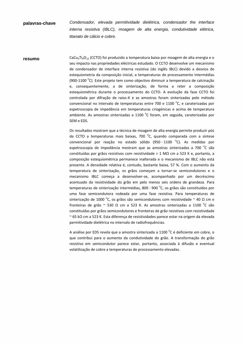
Condensador, elevada permitividade dielétrica, condensador the interface
interna resistiva (IBLC), moagem de alta energia, condutividade elétrica,
titanato de cálcio e cobre.
CaCu3Ti4O12 (CCTO) foi produzido a temperatura baixa por moagem de alta energia e o
seu impacto nas propriedades eléctricas estudado. O CCTO desenvolve um mecanismo
de condensador de interface interna resistiva (do inglês IBLC) devido a desvios de
estequiometria da composição inicial, a temperaturas de processamento intermédias
(900-1100 oC). Este projeto tem como objectivo diminuir a temperatura de calcinação
e, consequentemente, a de sinterização, de forma a reter a composição
estequiométrica durante o processamento do CCTO. A evolução da fase CCTO foi
controlada por difração de raios-X e as amostras foram sinterizadas pelo método
convencional no intervalo de temperaturas entre 700 e 1100 oC, e caraterizadas por
espetroscopia de impedância em temperaturas criogénicas e acima de temperatura
ambiente. As amostras sinterizadas a 1100 oC foram, em seguida, caraterizadas por
SEM e EDS.
Os resultados mostram que a técnica de moagem de alta energia permite produzir pós
de CCTO a temperaturas mais baixas, 700 oC, quando comparada com a síntese
convencional por reação no estado sólido (950.-.1100 oC). As medidas por
espetroscopia de impedância mostram que as amostras sinterizadas a 700 oC são
constituídas por grãos resistivos com resistividade > 1 MΩ cm a 523 K e, portanto, a
composição estequiométrica permanece inalterada e o mecanismo de IBLC não está
presente. A densidade relativa é, contudo, bastante baixa, 57 %. Com o aumento da
temperatura de sinterização, os grãos começam a tornar-se semicondutores e o
mecanismo IBLC começa a desenvolver-se, acompanhado por um decréscimo
acentuado da resistividade do grão em pelo menos seis ordens de grandeza. Para
temperaturas de sinterização intermédias, 800.-.900 oC, os grãos são constituídos por
uma fase semicondutora rodeada por uma fase resistiva. Para temperaturas de
sinterização de 1000 oC, os grãos são semicondutores com resistividade ~ 40 Ω cm e
fronteiras de grão ~ 530 Ω cm a 523 K. As amostras sinterizadas a 1100 oC são
constituídas por grãos semicondutores e fronteiras de grão resistivos com resistividade
~ 65 kΩ cm a 523 K. Esta diferença de resistividades parece estar na origem da elevada
permitividade dielétrica no intervalo de radiofrequências.
A análise por EDS revela que a amostra sinterizada a 1100 oC é deficiente em cobre, o
que contribui para o aumento da condutividade do grão. A transformação do grão
resistivo em semicondutor parece estar, portanto, associada à difusão e eventual
volatilização de cobre a temperaturas de processamento elevadas.
keywords
Capacitor, high dielectric permittivity, Internal Barrier Layer Capacitor (IBLC),
high-energy milling, electric conductivity, calcium copper titanate.
Abstract
CaCu3Ti4O12 (CCTO) powders were produced at low temperatures by high-energy ball
milling and its impact on the electrical properties of CCTO ceramics carried out. CCTO
ceramics develop an internal barrier layer capacitance (IBLC) mechanism due to small
changes in stoichiometry, which seems to start at intermediate processing
temperatures (900.-.1100.oC). This project aims to decrease the calcination and
sintering temperatures to retain the stoichiometric composition during processing of
CCTO ceramics. The evolution of the CCTO phase was evaluated by X-ray diffraction
and ceramics were prepared by conventional sintering at temperatures between 700
and 1100 oC. The samples were characterised by impedance spectroscopy at
subambient and high temperatures. Ceramics sintered at 1100 oC were characterised
by SEM and EDS.
The results show that high-energy ball milling permits the production of CCTO powder
at lower temperature, 700.oC, compared to conventional solid state reaction
(950.-.1100.oC). Impedance spectroscopy measurements show that ceramics sintered
at a temperature of 700.oC, the stoichiometric composition of CCTO is retained and
consists of insulating grains with a resistivity > 1 MΩ cm at 523 K. The relative density
is, however, rather low, 57 %, and the IBLC mechanism is not present in this sample as
usually observed for CCTO ceramics. When the sintering temperature increases, the
insulating grains start to transform into semiconducting and the IBLC mechanism starts
to appear, accompanied by a significant drop on the resistivity by at least six orders of
magnitude for ceramics sintered at 1000 oC. At intermediate sintering temperatures,
800 - 900.oC, the grains are electrically heterogeneous containing both insulating and
semiconducting phases. When samples are sintered at 1000 oC, the grains are totally
semiconducting with resistivity of ~ 40 Ω cm and grain boundary resistivity of ~
530.Ω.cm at 523 K. Ceramics sintered at 1100 oC exhibit semiconducting grains
surrounded by insulating grain boundary with resistivity of ~ 65 kΩ cm at 523 K, and
this seems to be responsible for the high effective permittivity at radio frequencies for
dense ceramics.
The EDS analysis shows CCTO ceramics sintered at 1100 oC to be Cu-deficient and it
contributes to the increase of the bulk conductivity. The transformation of the resistive
into semiconducting grains and the evolution of the IBLC mechanism may be,
therefore, linked to the diffusion and eventual volatilisation of copper at elevated
processing temperatures.
Contents
List of figures i
List of tables iii
List of symbols and abbreviations iv
1. Introduction 1
1.1. Perovskite compounds 2
1.2. Perovskite structure 2
1.2.1. Ideal cubic perovskite structure 2
1.2.2. Structural distortions on perovskites 3
1.2.2.1. Size effects 3
1.2.2.2. Deviation from the ideal ABX3 composition 4
1.2.3. Distortion of the ideal cubic perovskite 5
1.2.3.1. Tilting of octahedra 5
1.2.4. Double perovskites 6
1.2.5. Glazer notation
1.3. ACu3Ti4O12 compounds
1.4. CaCu3Ti4O12
1.5. Physical properties of CCTO
1.6. Ferroelectric BaTiO3
1.6.1. Structural considerations of CCTO
1.7. High dielectric permittivity of CCTO 12
1.7.1. Non-ohmic contacts 12
1.7.2. Internal barrier layer capacitance (IBLC) 14
1.7.2.1. Oxygen non-stoichiometry model 16
1.7.2.2. Cation non-stoichiometry model 16
1.8. Influence of microstructure on the electrical properties
of CCTO ceramics 17
1.9. Doping effects in CCTO ceramics 19
1.10. Aim of this work 20
2. Experimental procedure 22
2.1. Preparation and structural characterisation of CCTO powders
2.2. Phase analysis of calcined powder
2.3. CCTO ceramic processing
2.4. Electrical characterisation 24
2.4.1. Impedance spectroscopy 24
23
22
22
22
20
19
17
16
16
14
12
12
11
10
9
8
7
7
5
5
4
3
3
2
2
2
1
iv
iii
i
2.4.2. Fundaments of impedance spectroscopy 24
2.4.2.1. Theory 25
2.4.2.2. Impedance response of circuit elements 27
2.4.2.3. Impedance formalisms 27
2.4.2.4. Combined ideal circuit elements 28
2.4.2.5. Single parallel RC element 29
2.4.2.6. Two parallel RC elements in series 31
2.4.2.7. The Brickwork Layer Model 33
2.4.2.8. Arrhenius plots 33
2.5. Microstructural characterisation 34
3. Results and discussion 34
3.1. Results 35
3.1.1. Structural and microstructural characterisation of CCTO 35
3.1.2. Electrical characterisation of CCTO ceramics 37
3.2. Discussion 51
4. Conclusion 54
5. Future work 55
References 56
34
35
i
List of figures
Figure 1.1 – Schematic of the Pm3m perovskite structure including an outline of the cubic unit
cell. The BX6 units are represented as octahedra with B atoms visible within them, and the A ion
centrally located in the cube-octahedral cavity between the octahedra. 3
Figure 1.2 - Illustration of a transition from a simple cube to the ordered and asymmetric body-
centered tetragonal unit cell. 6
Figure 1.3 – Representation of the CCTO unit cell. 8
Figure 1.4 – Variation of the dielectric permittivity of (a) BT and (b) CCTO with temperature,
at 1 MHz.
Figure 1.5 – BT unit cell displaying Ti4+ displacement. 10
Figure 1.6 – Energy band diagrams for a metal and an n-type semiconductor: (a) the two materials
are separated and (b) the materials are in contact. 13
Figure 1.7 – Representation of the simplified IBLC: tb is the bulk thickness, tgb the grain boundary
thickness and L the sample thickness. 14
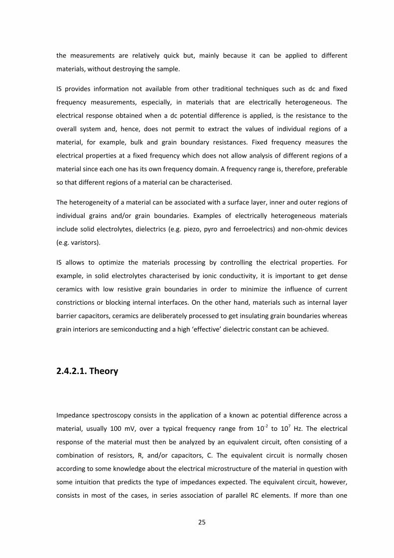
Figure 2.1 – Schematic of two parallel RC elements connected in series. 26
Figure 2.2 – Typical Z* impedance plot. 28
Figure 2.3 – Typical Z* plot and equivalent circuit for a single parallel RC element. 29
Figure 2.4 – Typical combined Z’’ and M’’ spectroscopic plot for a single RC element. 30
Figure 2.5 - Typical Z* plot and equivalent circuit for two parallel RC elements connected in
series. 31
Figure 2.6 –Typical Z’’ and M’’ spectroscopic plot for two parallel RC elements connected in
series. 32
Figure 3.1 – XRD pattern of powders after milling for 1, 2, 4, 6 and 10 h, and after calcination at
650 and 700 oC.
Figure 3.2 – BEI and EDS of (a) main-phase and (b) inclusion of CCTO 1100 ceramics. 37
Figure 3.3 – Z* plots of CCTO 700, 800 and 900 ceramics at 523 K. 38
Figure 3.4 – Z* plots for (a) CCTO 1000 and (b) CCTO 1100 ceramics at 523 K. 39
Figure 3.5 – Z* plots for CCTO 1000 and CCTO 1100 at 80K. 40
Figure 3.6 – C spectroscopic plots for all samples at 523 K. 41
29
31
30
41
36
9
ii
Figure 3.7 – C spectroscopic plots of (a) CCTO 1000 and (b) CCTO 1100 samples at 10, 100 and
320 K. 42
Figure 3.8 – M’’ spectroscopic plots for (a) CCTO 700, (b) for CCTO 800 and (c) for CCTO 900 at
subambient temperatures. The measurement temperatures are shown in the label. 44
Figure 3.9 – M’’ spectroscopic plots of CCTO for all samples at 523 K. An enlargement of the high
capacitance region for CCTO 1000 and CCTO 1100 is shown in the inset. 45
Figure 3.10 – M’’ spectroscopic plot for CCTO 1000 and CCTO 1100 at 80 K. 46
Figure 3.11 – Arrhenius plots comparing σb and σgb for all CCTO samples: (a) at high
temperatures and (b) at low temperatures. 47
Figure 3.12 – Representation of the maximum frequency of M’’max peak with temperature for all
samples. 48
Figure 3.13 – Ratio between semiconducting and total phase (semiconducting + resistive phases)
for samples sintered between 800 and 1100 oC.
49
48
47
42
iii
List of tables Table 1 – Relative dielectric constant and loss tangent for ACu3B4O12 compounds, at 100 kHz
(25.oC). 7
Table 2 - Possible phenomena and their typical capacitance values. 29
Table 3 – Identification of the samples sintered at different temperatures and respective relative
density. 35
Table 4 – Summary of the results for the activation energy and resistivity and capacitance
extracted from Z’’ vs Z’ and M’’ at 523 K. 50
Table 5 – Summary of the results for the capacitance and resistivity of the samples, at 80 K,
extracted from Z’’ vs Z’ and M’’. The table also provides the ratio between the semiconducting
and total phases. 50
iv
List of symbols and Abbreviations Symbols
a - lattice parameter
A – sample sectional area
C - capacitance
Cb- bulk capacitance
Cgb – grain boundary capacitance
d - spacing between planes in the atomic lattice
dtheoretical – theoretical density
%d – relative density
Ea –activation energy
f – frequency
I – current intensity
k - Boltzmann constant (1,38x10⁻²³ J K-1)
L – sample thickness
MA – Atomic mass
M’’ – real part of electric modulus
M*- electric modulus
n – Layers index number
NA – atomic number
r – ionic radii
R – resistivity
Rb – bulk resistivity
Rgb – grain boundary resistivity
t – tolerance factor
Tc – curie temperature

v
tb – bulk thickness
tgb – grain boundary thickness
T - absolute temperature
V – potential difference
Vcell – unit cell volume
Y* - admittance
Z’ – real part of impedance
Z’’ – imaginary part of impedance
Z – impedance of a circuit element
Z* - impedance
ℇ0 - permittivity of vacuum (8.854x10⁻¹² F m-1)
ℇ* - permittivity
ℇeff – effective permittivity
ℇr – intrinsic or bulk permittivity
ϴ - angle between the incident ray and scattering planes
λ – wavelength
σ - conductivity
σ0 - pre-exponential factor of conductivity
τ – time constant
Фm – work function of the metal
Фs – effective work function of the semiconductor
ω – angular frequency
vi
Abbreviations
ac – alternating current
ABX3 - general formula of a perovskite
BCTO - Bi2/3Cu3Ti4O12
BEI - backscattered electron image
BLM - Brickwork Layer Model
BT – BaTiO3
CCTO – CaCu3Ti4O12
CCTO 700 – sample sintered at 700 oC
CCTO 800 – sample sintered at 800 oC
CCTO 900 – sample sintered at 900 oC
CCTO 1000 – sample sintered at 1000 oC
CCTO 1100 – sample sintered at 1100 oC
CCMTO - CaCu2.94Mn0.06Ti4O12
dc - direct current
DRAM - Dynamic Random Access Memory
EDS - energy-dispersive X-ray spectroscopy
HEBM - high-energy ball milling
IBLC - Internal Barrier Layer Capacitor
IS - impedance spectroscopy
SEM - scanning electron microscopy
ST - SrTiO3
TG - thermogravimetric analysis
XRD - X-ray diffraction
YCTO - Y2/3Cu3Ti4O12
YSZ - yttria-stabilized zirconia
1
1. Introduction
Nowadays, a big challenge in the microelectronics industry is to decrease the size of the passive
components, especially, the capacitors. Materials with high dielectric constant have been,
therefore, the target of attention. Since the discovery of ferroelectricity in single crystals of
Rochelle salt in 19211, much work has been done to find new materials possessing high dielectric
constant. During the World War II, the study of ferroelectrics increased rapidly with the discovery
of Barium titanate (BaTiO3). Most materials with high dielectric constant have ferroelectric
characteristics such as BaTiO3 2, a classic material used in the capacitor industry, due to an atomic
displacement of Ti4+ within the unit cell. These materials possessing ferroelectric characteristics
display some disadvantages since the dielectric constant is dependent on the temperature,
reaching a maximum at a fixed temperature, known to as the Curie temperature. Above the Curie
temperature a phase transition occurs, accompanied by an abrupt decrease on the dielecric
permittivity, compromising the use of BaTiO3 for some applications such as capacitores3.
Therefore, a new class of materials with non-ferroelectric characteristics but exhibiting high
dielectric permittivity has been extensively studied in recent years. It is the case of CaCu3Ti4O12
(CCTO), a non-ferroelectric material, which exhibits a ‘giant’ dielectric constant of about 104 to 105
and stable over a wide temperature range from 100 to 600 K.4,5 However, CCTO exhibits high
dielectric losses at high frequencies (> MHz), where the dielectric constant drops down to 100.
Due to these characteristics, CCTO can be used in the manufacture of electronic components such
as multilayer capacitors, electronic devices such as DRAM and microwave devices.6,7 There are
also other materials that have large dielectric constant and similar electric behaviour as CCTO,
such as Bi2/3Cu3Ti4O12 (BCTO), Y2/3Cu3Ti4O12 (YCTO), among others.
CCTO has high dielectric constant due to an internal barrier layer capacitance (IBLC) mechanism.
This effect, however, is poorly understood, since questions regarding the development of the
n-type semiconductivity as well as the effect of processing on the electrical properties of CCTO
ceramics are still unclear. Changing the synthesis technique in the preparation of CCTO powder
with high purity may be helpful to the understanding of the effect of processing on the final
electrical properties of CCTO ceramics.
In this work, CCTO powders were produced by a different synthesis method, high-energy ball
milling, in order to decrease the calcination and sintering temperatures and study the effect on
the electrical properties of ceramics by impedance spectroscopy (IS).
2
1.1. Perovskite compounds
There is a wide variety of compounds that have the perovskite structure due to its flexibility to
accommodate almost all elements in the periodic table. Most of them are oxides and fluorides
and can be composed from many combinations of anions and cations. This diversity results in a
broad range of physical properties (dielectric, magnetic, optical, etc) and, therefore, different
technological applications. For example, BaTiO3 is a ferroelectric material with high dielectric
constant near its Curie temperature and hence, an important material in the capacitor industry.
Ba(Bi1-xPbx)O3 is used for the production of superconductors, La1-xCaxMnO3 is a material which
displays magnetoresistive and magnetostrictive properties and so on.8 For these reasons,
perovskite structured compounds have been extensively studied for many years.
1.2. Perovskite structure
The general formula for a perovskite compound is ABX3 in which F-, Cl- and O2- can be
incorporated into the structure in the X position 9. The perovskite structure can be divided in two
main groups: the ideal cubic perovskite and distorted cubic perovskite which corresponds to most
of ABX3 compounds.10,11
1.2.1. Ideal cubic perovskite structure
The ideal cubic perovskite structure belongs to the cubic space group Pm3m, with coordination
number of six and twelve for the B and A cations, respectively. X anion is coordinated by two B
cations and four A cations. An example of a compound with an ideal perovskite structure is
strontium titanate, SrTiO3.8,10,11
The most common description for the structure consists of a three-dimensional cubic network of
corner-sharing MX6 octahedra, where the A cation is in the center of a cube defined by eight
corner-sharing octahedral units with B in the center of each one. Note that all B-X-B and O-X-O
3
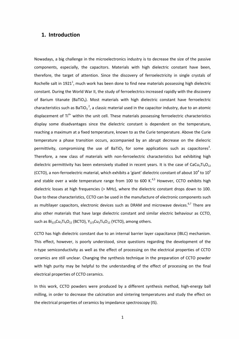
angles are 180 and 90o, respectively. Figure 1.1 illustrates the structure of a perovskite with the
description just mentioned.10
Most perovskite compounds, however, do not exhibit the ideal structure just described, but
instead they are distorted, usually, accompanied by loss of symmetry, which significantly affects
the physical properties. The type of distortion is important to understand the relation between
the crystal structure and physical properties of a material.
1.2.2. Structural distortions on perovskites
There are essentially three factors identified so far as contributing to the perovskite distortion:
size effects, deviations from the ideal composition and Jahn-Teller effects. These effects usually
act simultaneously in the distortion of the ideal cube.9
1.2.2.1. Size effects
In the ideal cube the cell axis, a, is geometrically related to the ionic radii (rA, rB and rO) according
to the equation: 9,12,13
(1)
Figure 1.1 – Schematic of the Pm3m perovskite structure including an outline of the
cubic unit cell. The BX6 units are represented as octahedra with B atoms visible
within them, and the A ion centrally located in the cube-octahedral cavity between
the octahedra.10
4
The ratio of the two expressions for the cell length is called the Goldschmidt’s tolerance factor t
and is a “measure” of the degree of distortion of a perovskite, described as follow:
(2)
The distortion happens when the A cation is too small and is not in contact with the anions
anymore. As a consequence the B-X-B bond bends slightly, tilting the BX6 octahedra in order to
keep the contact between anions and A cations. SrTiO3, an ideal perovskite, assumes naturally
t=1,00 with rA=1,44 Å, rB=0,605 Å and rO=1,40 Å. If the A ion is smaller than the ideal value then t
becomes smaller than 1. The cubic structure, however, remains if 0,89 < t < 1. For smaller values
the structure loses the symmetry. GdFeO3, for example, has t < 1 and the structure is
orthorhombic with rA=1,107 Å and rB=0,78 Å. For t < 0,8, the stable structure is ilmenite. The
tolerance factor can be more than 1 if the A cation is too large or the B cation too small and the
structure is hexagonal.9
1.2.2.2. Deviation from the ideal ABX3 composition
Deviation from the ideal ABX3 composition occurs by having vacant sites which would normally be
occupied or the cations have different valency. This is the case for SrFeOy (2,5 ≤ y ≤ 3) where the
valency of Fe changes as it is heated in an oxidizing or reducing atmosphere. When y < 3, SrFeOx is
composed of a mixture of Fe3+ and Fe4+ ions. This is a common example of a defect perovskite in
which deviations from the ideal composition results in distorted perovskites.9
The existence of tetragonal, orthorhombic, rhombohedral, monoclinic and triclinic perovskites
arises, therefore, on the deviations from the ideal structure. In most cases, the substitution occurs
on the cation sites leading to a large class of compounds with the general formula AA’BB’X6. Such
substitutions can be made either in a random or ordered way. Usually the symmetry of ordered
perovskites is compromised and might lead, in many cases, to a change of the unit cell length.8
5
1.2.3. Distortion of the ideal cubic perovskite
The ideal perovksite structure can be distorted by three different mechanisms occurring
separately or in combination: distortions of octahedra, cation displacements within octahedra and
tilting of octahedra. The first two distortion mechanisms are due to electronic instabilities of the
octahedral metal ion. For example, the ferroelectric BaTiO3 displays an electronic instability that
leads to cation displacement of Ti4+ from the centre of the octahedron. Basically, cation
displacement is the movement of one or both A and B-site cations within the structure from their
respective symmetry sites, causing what is called ferroelectricity.8
Octahedral distortion involves no ion displacement, but instead, changes in the shape of the
octahedra by increasing or decreasing B-O bond length.
Octahedral tilting is the most common distortion in perovskites, representing 80.-.90 % of all
perovskites and is described in more detailed in the next section.14
1.2.3.1. Tilting of octahedra
As mentioned before, tilting of octahedra is seen in almost all perovskites and it occurs when the
A-site cation is too small for the cubic BX3 corner-sharing octahedral network. This distortion
consists of the tilting of BX6 about one or more of its symmetry axes and involves only the soft
B-X-B bond angle. Octahedral tilting usually does not change the coordination of the A cation,
however, there are four Glazer tilt systems that are an exception to this rule: a+a+a+, a+a+c-, a0b+b+
and a0b+b-, with the most important one being a+a+a+ tilting. The a+a+a+ tilt system is usually
present in perovskites with general formula of AA’3B4X12 and alters the coordination environment
of the A-site cation, leading to a four-coordinate square planar environment for A’ with short A’-X
bonds and a 12- coordinate icosahedral environment for A.3,8,10,14,15
Associated with a+a+a+ tilting is therefore an introduction of cation ordering and to date there are
approximately 40 AA’3B4X12 perovskites in which ordering of the A and A’ cations is stabilized by
a+a+a+ tilting. A corresponds to the larger cation and A’ to the smaller cation, for example, Cu2+
and Mn3+, respectively. The combination of octahedra tilting with cation ordering usually doubles
the length of the unit cell so changing the space group symmetry of the material.8,14
6
1.2.4. Double perovskites
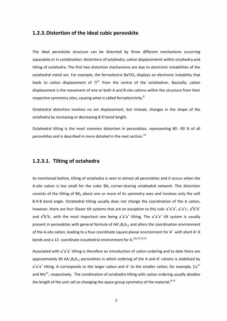
As mentioned in the section before, the combined effect of cation ordering and octahedral tilting
results in a double unit cell along the three crystallographic directions, to maintain the
translational symmetry. As a consequence, the space group of symmetry changes and in most
situations results in a loss of symmetry.8
Figure 1.2 illustrates the transition of a double unit cell from the simple cube to the ordered and
asymmetric body-centered tetragonal cell.
(a) illustrates an ideal cubic perovskite ABX3 before octahedral tilting; in (b) the face centered
tetragonal cell after an octahedral tilting distortion; in (c) the body-centered tetragonal cell and
(d) the ordered body-centered tetragonal cell, where the symmetry has been lost.8
To know how the octahedron tilts is fundamental to correlate with the electrical properties of
perovskite materials. A notation to characterise the tilting was developed by Glazer.
Figure 1.2 - Illustration of a transition from a simple cube to
the ordered and asymmetric body-centered tetragonal unit
cell.8
7
1.2.5. Glazer notation
Glazer described the octahedral tilting of different perovskite compounds, in 1972, giving rise to
23 different tilt (Glazer) systems. It consists of specifying the rotation of each axis of all three
cartesian axes by using two parameters (a#b#c#). The letters correspond to the magnitude of the
rotation around the [100], [010] and [001] directions of the Pm3m cubic perovskite and the
superscript # indicates if two adjacent octahedra rotate in the same or opposite direction and it
takes values of 0, + or -. 0 means there is no rotation about the axis, + indicates that adjacent
octahedra rotates in the same direction and - in the opposite direction.8,16 The most simple tilt
system is that of the ideal cubic perovskite Pm3m described previously; tilt system symbol is
a0a0a0, that is, there is no rotation around any axis.8,16
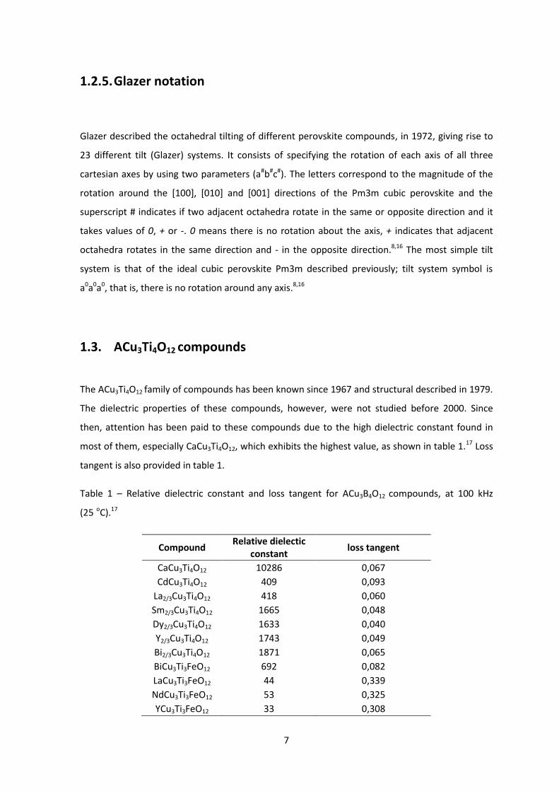
1.3. ACu3Ti4O12 compounds
The ACu3Ti4O12 family of compounds has been known since 1967 and structural described in 1979.
The dielectric properties of these compounds, however, were not studied before 2000. Since
then, attention has been paid to these compounds due to the high dielectric constant found in
most of them, especially CaCu3Ti4O12, which exhibits the highest value, as shown in table 1.17 Loss
tangent is also provided in table 1.
Table 1 – Relative dielectric constant and loss tangent for ACu3B4O12 compounds, at 100 kHz
(25.oC).17
Compound Relative dielectic
constant loss tangent
CaCu3Ti4O12 10286 0,067
CdCu3Ti4O12 409 0,093
La2/3Cu3Ti4O12 418 0,060
Sm2/3Cu3Ti4O12 1665 0,048
Dy2/3Cu3Ti4O12 1633 0,040
Y2/3Cu3Ti4O12 1743 0,049
Bi2/3Cu3Ti4O12 1871 0,065
BiCu3Ti3FeO12 692 0,082
LaCu3Ti3FeO12 44 0,339
NdCu3Ti3FeO12 53 0,325
YCu3Ti3FeO12 33 0,308
8
All these compounds crystallize in the perovskite-related structure and adopt the Im3 space group
symmetry, which is not common since tilting generally leads to the unit cell assymmetry.17
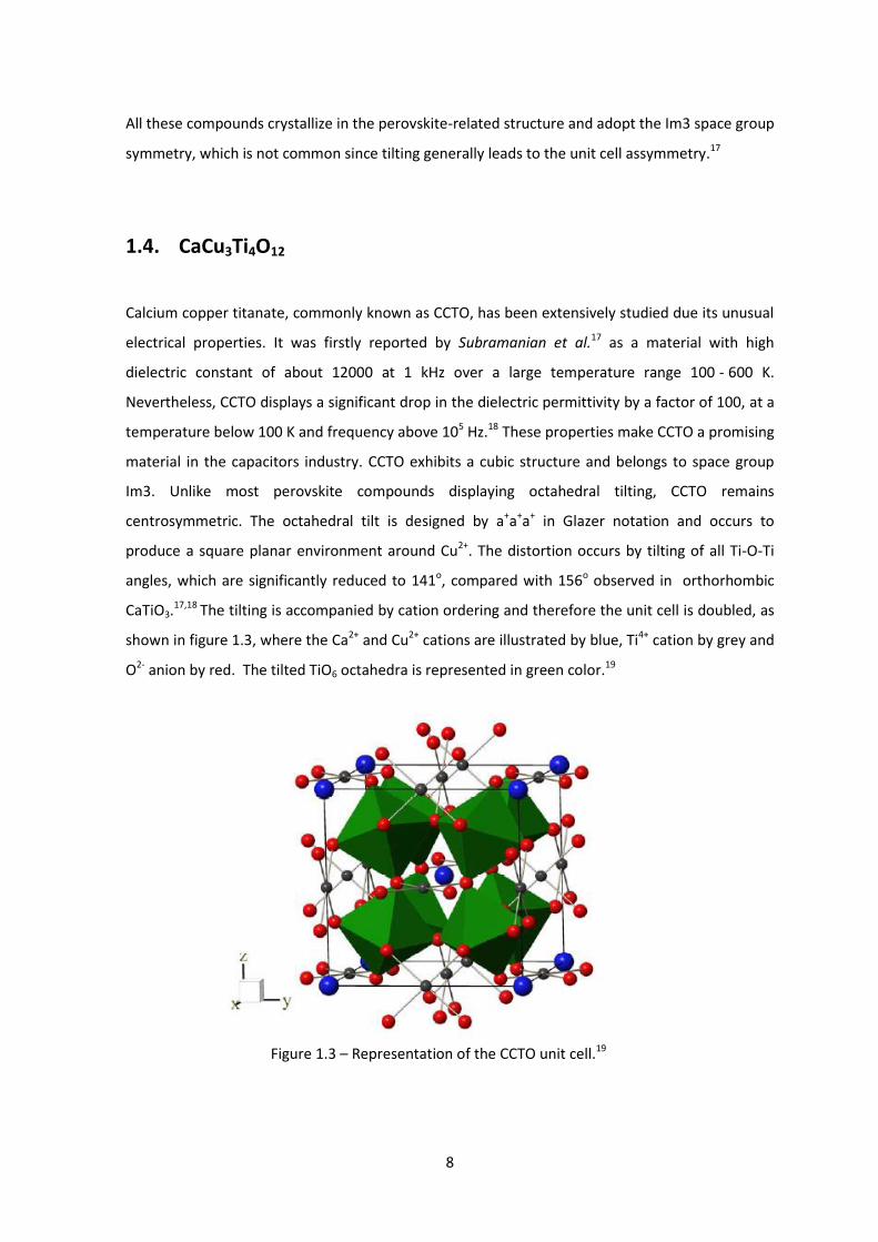
1.4. CaCu3Ti4O12
Calcium copper titanate, commonly known as CCTO, has been extensively studied due its unusual
electrical properties. It was firstly reported by Subramanian et al.17 as a material with high
dielectric constant of about 12000 at 1 kHz over a large temperature range 100.-.600 K.
Nevertheless, CCTO displays a significant drop in the dielectric permittivity by a factor of 100, at a
temperature below 100 K and frequency above 105 Hz.18 These properties make CCTO a promising
material in the capacitors industry. CCTO exhibits a cubic structure and belongs to space group
Im3. Unlike most perovskite compounds displaying octahedral tilting, CCTO remains
centrosymmetric. The octahedral tilt is designed by a+a+a+ in Glazer notation and occurs to
produce a square planar environment around Cu2+. The distortion occurs by tilting of all Ti-O-Ti
angles, which are significantly reduced to 141o, compared with 156o observed in orthorhombic
CaTiO3.17,18 The tilting is accompanied by cation ordering and therefore the unit cell is doubled, as
shown in figure 1.3, where the Ca2+ and Cu2+ cations are illustrated by blue, Ti4+ cation by grey and
O2- anion by red. The tilted TiO6 octahedra is represented in green color.19
Figure 1.3 – Representation of the CCTO unit cell.19
9
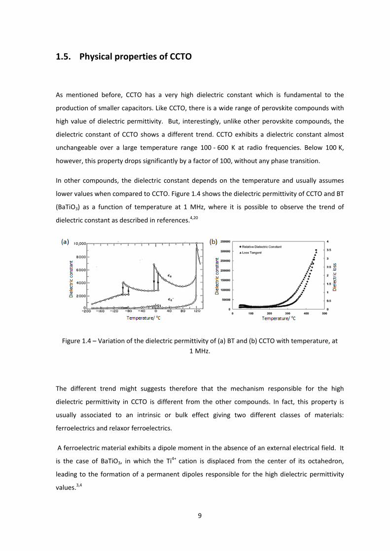
1.5. Physical properties of CCTO
As mentioned before, CCTO has a very high dielectric constant which is fundamental to the
production of smaller capacitors. Like CCTO, there is a wide range of perovskite compounds with
high value of dielectric permittivity. But, interestingly, unlike other perovskite compounds, the
dielectric constant of CCTO shows a different trend. CCTO exhibits a dielectric constant almost
unchangeable over a large temperature range 100.-.600 K at radio frequencies. Below 100.K,
however, this property drops significantly by a factor of 100, without any phase transition.
In other compounds, the dielectric constant depends on the temperature and usually assumes
lower values when compared to CCTO. Figure 1.4 shows the dielectric permittivity of CCTO and BT
(BaTiO3) as a function of temperature at 1 MHz, where it is possible to observe the trend of
dielectric constant as described in references.4,20
Figure 1.4 – Variation of the dielectric permittivity of (a) BT and (b) CCTO with temperature, at
1.MHz.
The different trend might suggests therefore that the mechanism responsible for the high
dielectric permittivity in CCTO is different from the other compounds. In fact, this property is
usually associated to an intrinsic or bulk effect giving two different classes of materials:
ferroelectrics and relaxor ferroelectrics.
A ferroelectric material exhibits a dipole moment in the absence of an external electrical field. It
is the case of BaTiO3, in which the Ti4+ cation is displaced from the center of its octahedron,
leading to the formation of a permanent dipoles responsible for the high dielectric permittivity
values.3,4
10
A relaxor ferroelectric material exhibits a ferroelectric response under higher electric fields at low
temperatures, but, without macroscopic spontaneous polarization.6 Unlike ferroelectrics, the
peak position of a relaxor ferroelectric material is a function of frequency and not accompanied
by a structural transition.17
CCTO does not exhibit any of these mechanisms. Hence, structural considerations must be taken
into account to understand why CCTO displays such a high dielectric constant. In the next section
the BaTiO3 structure, a classic ferroelectric material and widely used in the capacitor industry, is
compared with CCTO.
1.6. Ferroelectric BaTiO3
BaTiO3 (BT) has been used for more than 60 years due to its ferroelectric properties combined
with chemical and mechanical stability and ease of mass production.21 For this report, only the
ferroelectric properties of BT responsible for the high dielectric constant are discussed and
compared with CCTO.
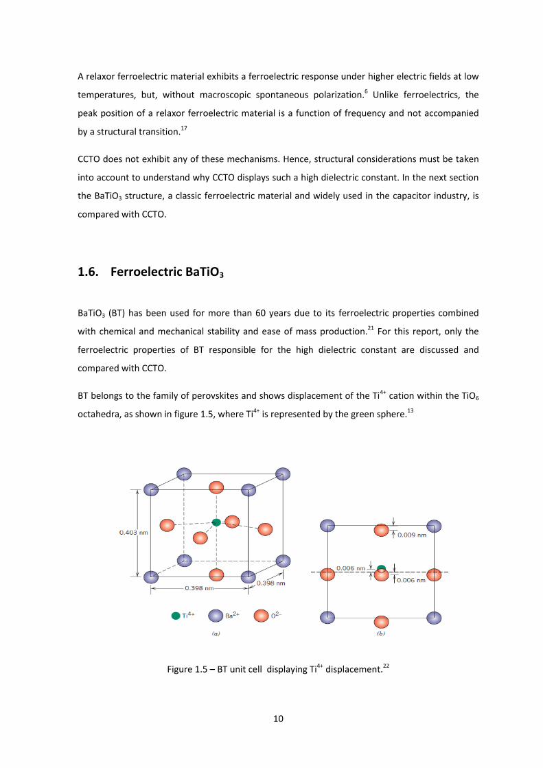
BT belongs to the family of perovskites and shows displacement of the Ti4+ cation within the TiO6
octahedra, as shown in figure 1.5, where Ti4+ is represented by the green sphere.13
Figure 1.5 – BT unit cell displaying Ti4+ displacement.22
11
BT displays spontaneous polarization because the Ti4+ is displaced off its central position, and it
has proved to be very successful in explaining its ferroelectric properties below the Curie
temperature (Tc ~ 120 oC). Above Tc the unit cell undergoes a phase transition to become cubic
and the high temperature non-polar phase is referred to as the paraelectric state, accompanied
by an abrupt decrease in the dielectric constant.21
The high dielectric constant of BT is associated with three structural phase transitions on
heating/cooling, each one corresponding to a peak, as shown in figure 1.4, section 1.5. The first
transition occurs from rhombohedral to orthorhombic at - 90 oC; the second occurs at - 5 oC and
transforms to tetragonal; finally and most important, at 120 oC (Tc), where the structure becomes
cubic. Above Tc, BT transforms to a paraelectric state, where the structure consists of a cubic cell
where all atoms occupy symmetric positions and, therefore, the ferroelectric state no longer
exists leading to a significant drop in the dielectric constant.17,21
The displacement of the Ti4+ cation occurs because Ba2+ is larger than Sr2+ (SrTiO3 is an ideal
perovskite as referred in the section 1.2.2.1) resulting in an expansion of the structure, with
increasing of Ti-O distance from 1,95 to 2 Å. The TiO6 octahedra is now too large for Ti4+ and Ti-O
bonds are under tension. On the other hand, the Ba-O distance of 2,99 Å based on the ionic radii
is much higher than the experimental value of 2,84 Å, suggesting that Ba2+ is in a site small for it.
This contributes to the increasing of polarizability of the TiO6 octahedra and therefore to the Ti4+
displacement.17
1.6.1. Structural considerations of CCTO
CCTO, on the other hand, does not display polarizability since all atoms in the unit cell occupy
symmetric positions. Therefore, CCTO is not a ferroelectric material. Like most perovskite
compounds, CCTO exhibits octahedral tilting, however, it remains centrosymmetric.
Like BT, the Ca-O distance of 2,84 Å in CCTO based on the ionic radii is much higher than the
experimental value of 2,60 Å. This also suggests that Ca2+ cation is in a site too small for it leading
to the expansion of unit cell and Ti-O bonds are under tension. However, the site symmetry for
Ti4+ in CCTO is much lower than that in cubic BT, reducing the possibility of any phase transition
based on the displacement of Ti4+ within the octahedra. Instead, the TiO6 octahedra have tilted to
form a square arrangement around Cu2+, in which the tilts are all in-phase, a+a+a+, according to
12
Glazer notation. In fact, Ti-O-Ti angles show a significant reduction of 141o compared to 156o
observed for CaTiO3.17,23
1.7. High dielectric permittivity of CCTO
The mechanism responsible for the high permittivity of ferroelectrics, based on structural
considerations, was discussed above. For CCTO no ferroelectric property has been found. So far,
this reason has attracted several researchers to try to understand why CCTO displays such high
dielectric permittivity.
Different models have been proposed to explain the origin of the high dielectric permittivity in
CCTO. Some of them suggest intrinsic models; however, most studies support an Internal Barrier
Layer Capacitance (IBLC) mechanism, an extrinsic model, as the main source responsible for the
high dielectric permittivity. Some researchers, however, link the high dielectric permittivity to a
non-ohmic electrode-semiconductor contact.
1.7.1. Non-ohmic contacts
A non-ohmic contact does not follow the Ohm’s law, V = RI, due to a mismatch in the Fermi level
at the interface between two materials with different composition, leading to the formation of a
blocking or Schottky barrier at the interface. This prevents the mobile charge carriers in the
junction of the two materials, giving rise to a high permittivity value. Figure 1.6 shows the energy
band for a metal and an n-type semiconductor, in separated and in contact. Фm represents the
work function of the metal and consists of the energy required to remove an electron with the
Fermi energy to the ‘vacuum level’. Фs represents the effective work function of the
semiconductor and corresponds to the energy difference between the Fermi energy and the
vacuum level. It is assumed for an n-type semiconductor that Фm> Фs. When the metal and
semiconductor are in contact, the electrons flow from the semiconductor to the metal until the
Fermi energy becomes constant. The electrons moving from the semiconductor to the interface
find an energy barrier (the Schottky barrier) of height |e|Ub, which determines the electrons
crossing the barrier and it is given by:
13
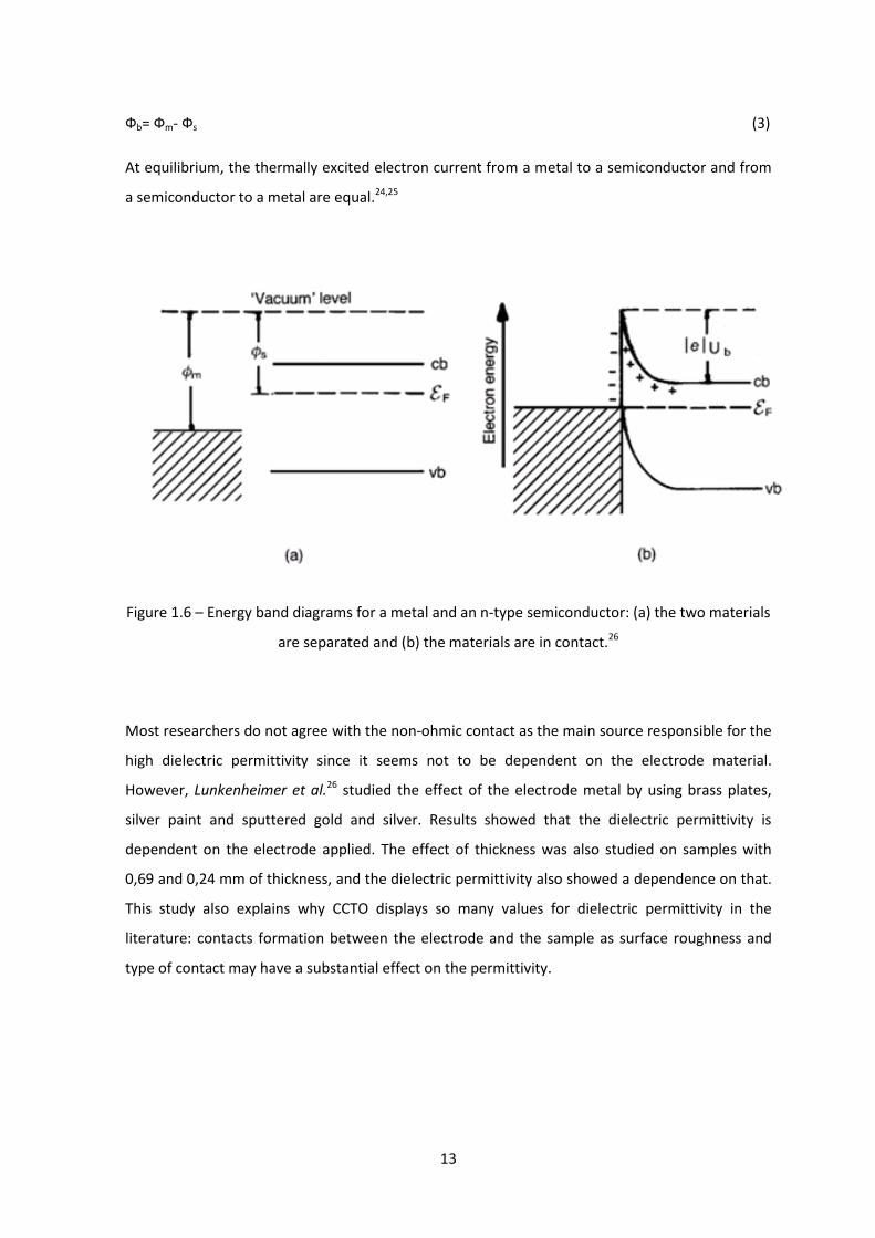
Фb= Фm- Фs (3)
At equilibrium, the thermally excited electron current from a metal to a semiconductor and from
a semiconductor to a metal are equal.24,25
Figure 1.6 – Energy band diagrams for a metal and an n-type semiconductor: (a) the two materials
are separated and (b) the materials are in contact.26
Most researchers do not agree with the non-ohmic contact as the main source responsible for the
high dielectric permittivity since it seems not to be dependent on the electrode material.
However, Lunkenheimer et al.26 studied the effect of the electrode metal by using brass plates,
silver paint and sputtered gold and silver. Results showed that the dielectric permittivity is
dependent on the electrode applied. The effect of thickness was also studied on samples with
0,69 and 0,24 mm of thickness, and the dielectric permittivity also showed a dependence on that.
This study also explains why CCTO displays so many values for dielectric permittivity in the
literature: contacts formation between the electrode and the sample as surface roughness and
type of contact may have a substantial effect on the permittivity.
14
1.7.2. Internal barrier layer capacitance (IBLC)
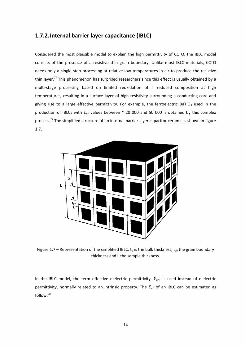
Considered the most plausible model to explain the high permittivity of CCTO, the IBLC model
consists of the presence of a resistive thin grain boundary. Unlike most IBLC materials, CCTO
needs only a single step processing at relative low temperatures in air to produce the resistive
thin layer.27 This phenomenon has surprised researchers since this effect is usually obtained by a
multi-stage processing based on limited reoxidation of a reduced composition at high
temperatures, resulting in a surface layer of high resistivity surrounding a conducting core and
giving rise to a large effective permittivity. For example, the ferroelectric BaTiO3 used in the
production of IBLCs with ℇeff values between ~ 20 000 and 50 000 is obtained by this complex
process.27 The simplified structure of an internal barrier layer capacitor ceramic is shown in figure
1.7.
Figure 1.7 – Representation of the simplified IBLC: tb is the bulk thickness, tgb the grain boundary
thickness and L the sample thickness.
In the IBLC model, the term effective dielectric permittivity, ℇeff, is used instead of dielectric
permittivity, normally related to an intrinsic property. The ℇeff of an IBLC can be estimated as
follow:28
15
(4)
where ℇr is the intrinsic permittivity of the material, tb and tgb are the thickness of the bulk and
grain boundary regions, respectively.
This model was supported by several studies where different techniques were applied in order to
understand the mechanism responsible for the high ℇeff. Sinclair et al. 29 studied the electrical
properties of CCTO using impedance spectroscopy, where data showed CCTO ceramics to be
electrically heterogeneous, consisting of semiconducting grains surrounded by insulating grain
boundaries. Grain and grain boundary resistivities at 300.K were 60.Ω.cm and 450.kΩ.cm,
respectively, consistent with an IBLC model. In terms of data, impedance complex plane plots, Z*,
at 300.K consist of a large arc at low frequencies with a non-zero intercept on the Z’ axis at high
frequency.
Kim et al.30 studied the dc bias dependence of the grain boundary resistance for different voltages
at 210 oC. The data showed that the interception of the large arc at high frequencies does not vary
with applied dc bias, consistent with the ohmic resistance in grains. The arc corresponding to the
grain boundary response, on the other hand, was shown to be dc bias dependent. The resistivity
decreases with increasing dc bias, indicating that Schottky barriers might be present at the grain
boundaries.
Chung et al.31 examined the presence of a potential barrier at the grain boundaries by using
microcontact current-voltage measurements. The I-V characteristics were directly measured
across individual grain boundaries and within the grains. Again, the grains obeyed Ohm’s law,
whereas, the I-V measured across grain boundaries was nonlinear, consistent with the presence
of an electrostatic barrier at the grain boundaries. In this work, the authors also determined the
breakdown of CCTO as a function of the grain size for samples sintered at 1100 oC for 3 and 20 h.
The breakdown voltage decreased significantly from 1300 to.300.V.cm-1, respectively. This
dependence is related to internal interfaces acting as electrical potential barriers and might be
the grain boundary.
Although the IBLC model is now widely accepted as the main source responsible for the high
effective permittivity in CCTO ceramics, questions relating to the development of the n-type
semiconductivity of CCTO are still unclear, since the formula CaCu3Ti4O12 corresponds to a
stoichiometric composition and, therefore, the grains should be insulating. Two models have been
proposed to explain the origin for bulk semiconductivity in CCTO ceramics.32 Both are, naturally,
16
based on non-stoichiometry of the bulk composition, occurring at the high temperatures required
for CCTO processing. Probably, the semiconducting grains appear during calcination in the
temperature range of 950.-.1100.oC and/or during the sintering process that requires high
temperature to get dense CCTO ceramics. The first model involves oxygen loss and the second is
based on cation non-stoichiometry. The difficulty in identifying the mechanism responsible for the
grain semiconductivity arises from the very small deviation of stoichiometry which is difficult to
detect by conventional techniques. For example, a CCTO sample was subjected to
thermogravimetric (TG) analysis up to 1100 oC showing no significant weight loss on heating and
cooling, confirming therefore that a small amount is lost, however, enough to induce bulk
semiconductivity in CCTO ceramics.29
1.7.2.1. Oxygen non-stoichiometry model
Oxygen loss is a plausible model to explain the origin of the bulk semiconductivity in CCTO
ceramics, based on a comparison with other titanate-based perovskites in which this
phenomenon is present when samples are processed at high temperatures and under
inert/reducing atmospheres. Basically, a small amount of oxygen is lost from the unit cell of CCTO
during processing in air at moderate temperatures, typically in the range of 900.-.1100 oC, with
subsequent compensation of oxygen vacancies by introduction of electrons into the Ti 3d band.
The oxygen lost to the atmosphere is represented by the following equation:
(5)
This process results in the general formula .32
1.7.2.2. Cation non-stoichiometry model
Cation non-stoichiometry comprises two steps, occurring separately. The first step on heating and
the second on cooling. During heating, a reduction of Cu2+ to Cu+ with subsequent charge
compensation by partial occupation of excess Ti4+ on the Cu sites occurs. The second step, on
17
cooling, consists of limited reoxidation of the monovalent copper to Cu2+ where the charge
compensation is ensured with electrons entering the Ti 3d conduction band and, therefore, a
partial reduction of Ti4+ to Ti3+ occurs. The following reactions describe, respectively, the first and
second steps:
(6)
(7)
The first reaction gives rise to the general formula and, the second,
to .32
1.8. Influence of microstructure on the electrical properties of CCTO
ceramics
As mentioned before, the high effective permittivity of CCTO ceramics is related to an IBLC where
a thin resistive layer at the grain boundaries seems to be responsible for this property. The eff has
been shown, however, to be dependent on the microstructure, which in turn depends on the
processing conditions of synthesis and sintering such as time, temperature, cooling rate and
oxygen partial pressure. This is why a wide range of values for eff (4 000 – 300 000) is reported in
the literature for CCTO ceramics.
It is well known from the fundaments of sintering that longer time and temperature of sintering
usually results in larger grains. Sinclair et al.27 studied the effect of the grain size on the eff, where
two samples were sintered at 1100.oC in air for 3 and 24 h. The average grain size was,
respectively, 5 and 100.µm, resulting in the enhancement of eff from ~ 9 000 to 280 000. Smaller
average grain sizes have a larger volume fraction of grain boundaries and therefore Schottky
barriers, resulting in an increase of the effective thickness of the charge storage regions, which
produces smaller values of eff. Nevertheless, the grain boundary resistivity decreased from 4,2 to
0,18.MΩ.cm. The bulk resistivity decreases from ~ 70 to 30 Ω.cm due to the decomposition of
CCTO as discussed in the section before. On the other hand, larger grains originate higher
dielectric losses.
18
In another study provided by Sinclair et al.28, sintered pellets were heat treated in N2 at 1000 oC.
The Z* plots showed the grain resistivity not to be dependent on the treatment with a
Rb ~ 60.Ω.cm. The grain boundary resistivity, however, decreased two orders of magnitude from
~ 450 to 7 kΩ cm, revealing that Rgb is dependent on the oxygen partial pressure of processing.
These results reveal that reoxidation of the grain boundary in air might occur on cooling,
producing a resistive thin layer responsible for high eff of CCTO ceramics.
He et al.33 studied the effect of cooling rate on the electrical properties. The permittivity of the
samples seems not to be dependent on the cooling rate. However, the grain boundary resistivity
is reduced as the cooling rate increases, and the dielectric loss rises. Apparently, the cooling rate
affects the reoxidation process causing changes in the electrical properties of CCTO ceramics.
Bender et al.34 prepared CCTO by conventional solid state reaction, mixing the initial reagents by
two different routes: via mortar and pestle and attrition-milling. It was observed that the high
permittivity of CCTO ceramics prepared via mortar and pestle were 11 700, much lower compared
to those prepared by attrition milling, 100 000. The effect of sintering temperature for ceramics
prepared by attrition-milling was also studied for 990 and 1050.oC, giving rise to dielectric
constants of 714 and 82 450, respectively.
Yang et al.35 studied the electrode/sample contact effects on the dielectric properties of CCTO
ceramics. They associated the high dielectric constant, in part, to the electrode/contact effects,
depending on the surface resistivity of the samples. For samples whose surface resistivity is higher
than 1,2 x 10⁸ Ω cm, the dielectric properties are independent of the metal electrodes and sample
thickness. A subsequent annealing of the samples in N2 atmosphere at 750 oC led to a decrease of
the surface resistivity down to 3,1.x.107 Ω cm, where the dielectric properties have become
changeable according to the metal electrodes. The dielectric constant of the sample with Pt
electrodes showed a higher value compared to that with Ag electrodes.
Kwon et al.36 have investigated the effects of cation stoichiometry on the electrical properties of
CaCu3-xTi4-yO12 (x= +0.06, 0, -0.06; y= +0.08, 0, -0.08) prepared by solid state reaction. X-ray
diffraction revealed that both Cu- and Ti-excessive CCTO compositions showed the presence of a
secondary Cu2O phase in the interior of non-stoichiometric CCTO ceramics giving rise to lower
dielectric constants compared with stoichiometric CCTO ceramics. The compositions
corresponding to Cu- and Ti-deficient CCTO showed no secondary phases and higher dielectric
constants and losses compared to the stoichiometric composition.
19
1.9. Doping effects in CCTO ceramics
Several doping studies of the initial composition of CCTO have been performed in order to
improve the electrical properties and at the same time to improve the understanding of the
electrical properties displayed by undoped CCTO ceramics. As mentioned before, CCTO is
electrically heterogeneous composed by a semiconducting grain and insulating grain boundary,
with permittivities of ~ 100 and 104.-.105, respectively. The typical activation energy of the bulk is
approximately 0,07 eV and grain boundary is in the range between 0,54 and 0,76 eV.
Interestingly, some works report some dopants to stabilize the composition at high temperatures
by keeping the bulk resistive with activation energy similar to the grain boundary of undoped
CCTO.
These results led researchers to believe that CCTO ceramics consist of bulk and grain boundary
regions with slightly different compositions. Li et al.32, prepared CCTO ceramics by doping with 2%
of Mn giving rise to the general formula CaCu2.94Mn0.06Ti4O12 (CCMTO). The electrical properties
were investigated by impedance spectroscopy and fixed frequency capacitance measurements.
The Z* plots for CCMTO at 473 K showed an absence of a nonzero intercept suggesting the bulk
resistance to be significantly higher for CCMTO ceramics. In fact, Arrhenius plots of the σg and σgb
for CCMTO showed that Rb is at least six orders of magnitude higher compared to that observed in
undoped CCTO ceramics. The activation energy increases from ~ 0,08 eV for CCTO to ~ 0,63 eV for
CCMTO, which is similar to that observed for the grain boundary in undoped CCTO ceramics. The
bulk conduction mechanism in CCMTO is, therefore, similar to that observed for the grain
boundary in CCTO. On the other hand, fixed frequency capacitance data showed that the ‘giant
permittivity’ observed in CCTO is not observed for CCMTO, suggesting once more the bulk
resistance to be much higher in CCMTO. These results may suggest that the origin for the
semiconductivity of grains in CCTO ceramics is based on a slightly different composition between
the grains and grain boundaries, however, enough to induce semiconductivity in the grains. In
addition, cation-nonstoichiometry may be a plausible explanation for the origin of the
semiconductivity. Partial substitution of Mn4+ instead of Ti4+ on the Cu sites may occur at high
temperatures in CCMTO: on cooling, reduction of Mn4+ to Mn3+ may occur to compensate for the
reoxidation of Cu+ in preference to partial reduction of the B-site Ti4+ to Ti3+ ions. This avoids the
introduction of electrons to the Ti 3d conduction band and therefore decreases substantially the
bulk semiconductivity.
20
Feng et al.37 studied the effects of La doping on the A’-site, Ca1-xLaxCu3Ti4O12 (x.=.0, 0.1, 0.2, 0.3,
0.4). They observed a decrease of the dielectric loss and dielectric constant as the La content
increases. Impedance spectroscopic data showed the bulk conductivity to increase with La doping,
while the grain boundary resistance remained nearly unchanged. The decrease in the dielectric
loss was explained by the decrease in the resistivity of CCTO grains/subgrains as La3+ acts as a
donor when it substitutes Ca2+, increasing the electron concentration and therefore a decrease of
the bulk resistance. In comparison, different results were obtained by Varma et al.38 In their study
of Ca1-xLa(2/3)xCu3Ti4O12 (x.=.0, 0.5,1), they concluded that La3+ substituting Ca2+ site resulted in the
decrease of the bulk and increase of the grain boundary conductivities with increasing of La3+
content. Consequently, a decrease of the internal barrier layer effect was observed.
Doping CCTO has therefore revealed that the electrical properties of CCTO ceramics can be
changed and controlled according to the properties desired. In addition, some works have shown
that it is possible to keep the bulk resistive with the activation energy similar to the grain
boundary of undoped CCTO ceramics and therefore, the conduction mechanism is similar. This led
researchers to believe that bulk and grain boundary may consist of similar but slightly different
compositions. At the same time, conventional techniques do not allow detection of variations in
the bulk composition as they are very small and, hence, it is difficult to understand the
mechanism responsible for the origin of the semiconducting grains. Therefore, no consensus is
seen in the literature reporting which mechanism is responsible for this phenomenon. Moreover,
these results lead researchers to believe that CCTO ceramics become unstable at intermediate
temperatures (900.-.1100.oC) and its process involving the synthesis and sintering methods may
be responsible for the appearance of semiconducting grains as always seen in the literature.
1.10. Aim of this work
Pure CCTO ceramics have been reported in the literature to consist of a semiconducting bulk
surrounded by a thin resistive layer at each grain boundary and hence, described as an internal
layer barrier capacitor (IBLC). CCTO, unlike most of compounds exhibiting these electrical
characteristics, needs only a single step of processing at relatively low temperatures in air. The
IBLC observed in most compounds is usually obtained by a multi-stage processing based on
21
limited reoxidation after a reducing process at high temperatures. This gives rise to the formation
of a resistive layer surrounding a conducting core responsible for the large effective permittivity.
The electrical properties of CCTO, however, are still unclear since the start composition of CCTO is
stoichiometric and therefore, the bulk should be resistive and not semiconducting. The literature
has always reported CCTO to be described by an IBLC model. Therefore, questions relating to the
processing of CCTO may be regarded in order to understand how it influences the electrical
properties of CCTO ceramics.
The processing of CCTO ceramics can be essentially comprised by the synthesis and sintering
processes. The most common method to synthesize CCTO powder is by solid state reaction.
However, the temperature required to get pure CCTO is in the range between 950 and 1100 oC
and it is possible that at these temperatures the grains become semiconducting. Therefore, other
methods have been applied to produce CCTO powder at lower temperatures 800.-.900.oC.
However, the sintering temperature required to get dense ceramics is very high at
~ 1000.-.1100.oC leading to the appearance of semiconducting grains.
The aim of this work is to produce CCTO powders by a non-conventional synthesis process at low
temperatures, high-energy ball milling, and to characterize its impact on the electrical properties
of CCTO ceramics. High-energy ball milling (HEBM) is a useful technique for synthesis of pure
nano-materials. This method is a simple method for oxides synthesis and it has been used to
produce homogenous and crystalline nanopowders. It is similar to the conventional solid state
reaction, consisting in a first step of milling of the precursors with subsequent calcination. The
difference is on the impact energy during milling. HEBM provides much higher impact energy due
to the higher velocity of milling and may be eventually up to 1000 times higher compared to that
achieved in conventional solid state reaction. This contributes for a reduction of crystallite size,
efficient mixing of precursors and mechanical activation by structural changes.39 This results in a
decrease of the calcination temperature to produce a single-phase compound.
The objective of this work is to produce CCTO powders at low temperatures by high-energy ball
milling and to understand if it is possible to produce pure CCTO ceramics with resistive bulk and,
therefore, how it influences the electrical properties of CCTO ceramics. The electrical
characterisation is provided using impedance spectroscopy (IS).
22
2. Experimental procedure
2.1. Preparation and structural characterisation of CCTO powders
Single phase CCTO was prepared by high-energy mechanochemical treatment of precursors: CuO
(Merck, 99.0 %), CaCO3 (Lancaster, 99.0 %) and TiO2 (Aldrich, 99.8 %) in stoichiometric quantities.
The reagents were weighed and mixed in a ball mill using yttria-stabilized zirconia grinding media
at 650 rpm for up to 10 hours. Excess heating was avoided by milling for periods of 10 minutes
with a pause for 3 minutes. The direction of rotation was reversed after each interruption. The
progress of structural changes or onset of reaction products was monitored by XRD analysis of
small fractions of the powders collected after different milling times.
The resulting powders obtained by mechanochemical treatment were calcined in air at 650 and
700 oC for 12 hours with a heating rate of 5 oC/min, to attempt complete conversion of precursor
reactants according to the chemical reaction:
CaCO3 (s) + 3 CuO (s) + 4 TiO2 (s) CaCu3Ti4O12 (s) + CO2 (g) (8)
The calcined powders were characterized by X-ray diffraction to monitor the presence of a single-
phase CCTO and to obtain the lattice parameters and theoretical density from the data.
2.2. Phase analysis of calcined powder
The phase purity of calcined powder was studied by X-ray diffraction on a Rigaku Geigerflex
diffractometer using Cu Kα1 radiation of wavelength 1,54059 Å. The powder was scanned in the
2 range 20 – 60 o.
From XRD data, the lattice parameter and the theoretical density were determined. The d-spacing
can be determined using Bragg’s law as follow:
23
nλ= 2d sin (9)
where n is the layers index number and usually takes value of 1, λ is the wavelength, d is the
spacing between planes in the atomic lattice and is the angle between the incident ray and
scattering planes.
CCTO belongs to the space group Im3 and, therefore, has a cubic unit cell structure. The relation
between the lattice parameter, a, and the d-spacing is:
(10)
The volume of the unit cell is:
Vcell=a3 (11)
And, finally, the theoretical density is:
(12)
where MA is the atomic mass and NA the atomic number.
2.3. CCTO ceramic processing
Green bodies of CCTO were pressed uniaxially in a steel die under an applied pressure of 200 MPa
and then, sintered on a platinum foil in a furnace (Lenton) at different temperatures (700, 800,
900, 1000 and 1100.oC) in air for 4 hours. The heating and cooling rates were 5.oC.min-1. After
sintering, the relative density of the pellets was measured from their geometry, according to the
following equation:
(13)
24
2.4. Electrical characterisation
2.4.1. Impedance spectroscopy
To study the effect of synthesis and sintering conditions on the electrical properties of CCTO
ceramics, impedance spectroscopy measurements were performed at high and subambient
temperatures, i.e, at temperatures below room temperature.
Prior to measurements, CCTO samples were polished to make parallel surfaces to provide a better
contact for the electrical measurements and the diameter and thickness of the pellets were
measured using a micrometer to determine the geometric factor, L/A (cm-1).
Subambient measurements were performed using an impedance analyzer (Agilent E4980) with an
applied ac voltage of 100 mV, over a frequency range of 20 Hz.- 2 MHz and a temperature range
of 10.-.320 K in a closed-cycle He refrigerator. InGa (60:40) alloy was used as electrode on both
faces of the pellet. IS data were corrected for sample geometry and analyzed using the
commercial software package ZVIEW.
For high temperatures, Au electrodes were sputtered on each pellet face on an Emitech K575XD
sputter coater. The measurements were taken in air using an Agilent 4294A impedance analyzer
with an applied ac voltage of 100 mV over a frequency range from 10 Hz.-.10 MHz and over a
temperature range from 300 to 700 K. Data were corrected for sample geometry and analyzed
using the commercial software package ZVIEW. The next sections provide the theory of
impedance spectroscopy.
2.4.2. Fundaments of impedance spectroscopy 19,40,41,42,43
Impedance spectroscopy (IS) is an important technique used to study correlations between
electrical properties and microstructural features of materials. It is widely used, in part, because
25
the measurements are relatively quick but, mainly because it can be applied to different
materials, without destroying the sample.
IS provides information not available from other traditional techniques such as dc and fixed
frequency measurements, especially, in materials that are electrically heterogeneous. The
electrical response obtained when a dc potential difference is applied, is the resistance to the
overall system and, hence, does not permit to extract the values of individual regions of a
material, for example, bulk and grain boundary resistances. Fixed frequency measures the
electrical properties at a fixed frequency which does not allow analysis of different regions of a
material since each one has its own frequency domain. A frequency range is, therefore, preferable
so that different regions of a material can be characterised.
The heterogeneity of a material can be associated with a surface layer, inner and outer regions of
individual grains and/or grain boundaries. Examples of electrically heterogeneous materials
include solid electrolytes, dielectrics (e.g. piezo, pyro and ferroelectrics) and non-ohmic devices
(e.g. varistors).
IS allows to optimize the materials processing by controlling the electrical properties. For
example, in solid electrolytes characterised by ionic conductivity, it is important to get dense
ceramics with low resistive grain boundaries in order to minimize the influence of current
constrictions or blocking internal interfaces. On the other hand, materials such as internal layer
barrier capacitors, ceramics are deliberately processed to get insulating grain boundaries whereas
grain interiors are semiconducting and a high ‘effective’ dielectric constant can be achieved.
2.4.2.1. Theory
Impedance spectroscopy consists in the application of a known ac potential difference across a
material, usually 100 mV, over a typical frequency range from 10-2 to 107 Hz. The electrical
response of the material must then be analyzed by an equivalent circuit, often consisting of a
combination of resistors, R, and/or capacitors, C. The equivalent circuit is normally chosen
according to some knowledge about the electrical microstructure of the material in question with
some intuition that predicts the type of impedances expected. The equivalent circuit, however,
consists in most of the cases, in series association of parallel RC elements. If more than one
26
electrical region in a material is present, for example, grain and grain boundaries are electrically
different, they are usually connected in series, as shown in figure 2.1. The RbCb models the
electrical response of the grain and RgbCgb the grain boundary response. The overall sample
resistance is the summation of Rb and Rgb which corresponds to the resistance obtained using dc
electrical measurements.
Figure 2.1 – Schematic of two parallel RC elements connected in series.
Some materials may show an additional electrical response due to the presence of other electro-
active regions, for example, outer surface layers and electrode/sample contacts. This is usually
described as a parallel RC element placed in series with those used to model the bulk and grain
boundary regions.
Each element is composed by a resistive component, corresponding to the resistance, and a
reactive component, corresponding to the capacitance and/or inductance. The inductance
displays, however, a minimal effect in non-magnetic materials and can therefore be ignored. The
reactance is therefore represented only by the capacitor.
Each region of a material is characterised by a relaxation time or time constant, τ, given by the
following equation:
τ =RC = 1/ωmax (14)
where ωmax=2πfmax is the angular frequency of the maximum loss. These parameters are
important since they are independent of the geometry of a region within the material.
27
2.4.2.2. Impedance response of circuit elements
The impedance of a circuit element is defined by:
Z= ΔV/ΔI (15)
For a pure resistor, the resistance follows the Ohm’s law:
R=V/I (16)
where V is the potential difference and I the current intensity. The response is not dependent on
the potential difference, i.e, it is the same under an ac or a dc potential field.
On the other hand, capacitors and inductors are dependent on the applied frequency (ω)
according to the equations, respectively:
XC=1/ωC (17)
XL= ωL (18)
C is the capacitance and L the inductance.
2.4.2.3. Impedance formalisms
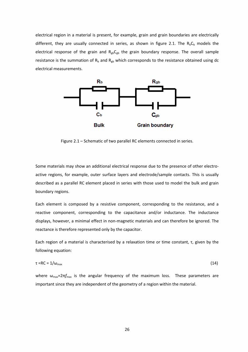
IS data can be represented by different formalisms, each one highlighting a different aspect of the
data. There are four different possible formalisms: impedance Z*, admittance Y*, permitivity ℇ*,
and electric modulus M*. The most common plot is that one represented by impedance,
Z*=.Z.-.Z’’ which has a real part, Z’, and an imaginary part, Z’’. The amplitude of Z’ is related to the
resistive part and the peak of Z’’ to the capacitor. Figure 2.2 shows a general impedance plot.
28
Figure 2.2 – Typical Z* impedance plot.
The others complex formalisms are represented by:
M*= jC0Z* (19)
*= 1/M* (20)
Y*=jC0 * = 1/Z* (21)
where C0(L/A)=0=8.854x10-12 F m-1 is the permittivity of vacuum.
2.4.2.4. Combined ideal circuit elements
Different regions of a material are characterised by different values of resistance and capacitance,
usually placed in parallel. When the corresponding relaxation frequencies 1/(RiCi) differ by orders
of magnitude, each parallel RC element gives rise to a semicircle from which the values of R and C
can be extracted. The value of R is obtained from the interception of the semicircle on the Z’ axis
and, C, using the equation (14) at the maximum of each semicircle.
The determination of the capacitance values is very important, since each region in a material has
its own typical values and, therefore, it is possible to assign the capacitance to the respective
region. Table 2 shows typical capacitance values for different phenomena within a material.
29
Table 2 - Possible phenomena and their typical capacitance values.19
Phenomenon responsible Capacitance/ F cm-1
Bulk Minor, second phase Grain boundary Bulk ferroelectric near Tc (Curie Temperature) Surface layer Sample-electrode interface Electrochemical reactions
10-12 10-11 10-11 - 10-8 10-10 - 10-9 10-9 - 10-7 10-7 - 10-5 10-4
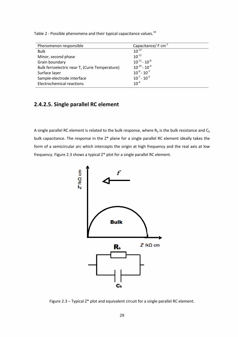
2.4.2.5. Single parallel RC element
A single parallel RC element is related to the bulk response, where Rb is the bulk resistance and Cb
bulk capacitance. The response in the Z* plane for a single parallel RC element ideally takes the
form of a semicircular arc which intercepts the origin at high frequency and the real axis at low
frequency. Figure 2.3 shows a typical Z* plot for a single parallel RC element.
Figure 2.3 – Typical Z* plot and equivalent circuit for a single parallel RC element.
30
The semicircle associated with the bulk response in the Z* plots is usually depressed and
therefore deviates from the ideal behaviour. This may be associated with the presence of a
distribution in relaxation times within the bulk response and distortion by other relaxations, e.g.,
grain boundary relaxations, whose time constants are within two orders of magnitude of that of
the bulk.
From the Z* plot it is possible to extract the value of R which corresponds to the diameter of the
semicircle, also equal to the low frequency intercept on the Z’-axis or double the height of Z’’max. A
geometry correction, L/A (cm-1), is applied so that R and C values for different samples from the
same or different materials can be compared.
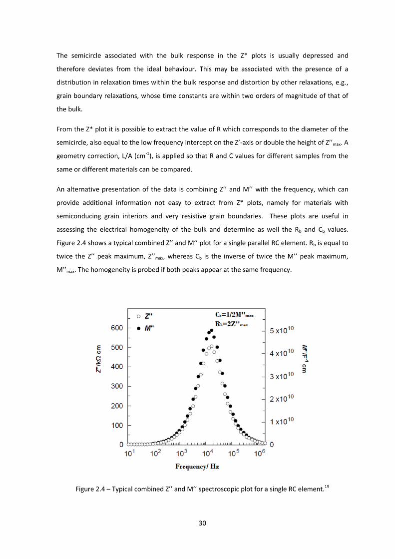
An alternative presentation of the data is combining Z’’ and M’’ with the frequency, which can
provide additional information not easy to extract from Z* plots, namely for materials with
semiconducing grain interiors and very resistive grain boundaries. These plots are useful in
assessing the electrical homogeneity of the bulk and determine as well the Rb and Cb values.
Figure 2.4 shows a typical combined Z’’ and M’’ plot for a single parallel RC element. Rb is equal to
twice the Z’’ peak maximum, Z’’max, whereas Cb is the inverse of twice the M’’ peak maximum,
M’’max. The homogeneity is probed if both peaks appear at the same frequency.
Figure 2.4 – Typical combined Z’’ and M’’ spectroscopic plot for a single RC element.19
31
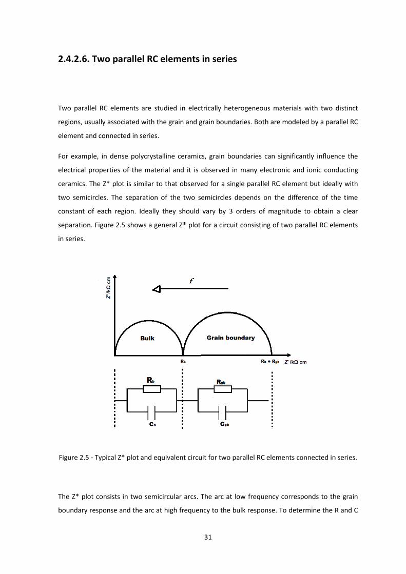
2.4.2.6. Two parallel RC elements in series
Two parallel RC elements are studied in electrically heterogeneous materials with two distinct
regions, usually associated with the grain and grain boundaries. Both are modeled by a parallel RC
element and connected in series.
For example, in dense polycrystalline ceramics, grain boundaries can significantly influence the
electrical properties of the material and it is observed in many electronic and ionic conducting
ceramics. The Z* plot is similar to that observed for a single parallel RC element but ideally with
two semicircles. The separation of the two semicircles depends on the difference of the time
constant of each region. Ideally they should vary by 3 orders of magnitude to obtain a clear
separation. Figure 2.5 shows a general Z* plot for a circuit consisting of two parallel RC elements
in series.
Figure 2.5 - Typical Z* plot and equivalent circuit for two parallel RC elements connected in series.
The Z* plot consists in two semicircular arcs. The arc at low frequency corresponds to the grain
boundary response and the arc at high frequency to the bulk response. To determine the R and C
32
values for each region, the two semicircular arcs are treated separately, with the same method
used for a single parallel element. The only difference is for determining the Rgb, since the lowest
frequency intercept on the Z’ axis is equal to the summation of Rb and Rgb.
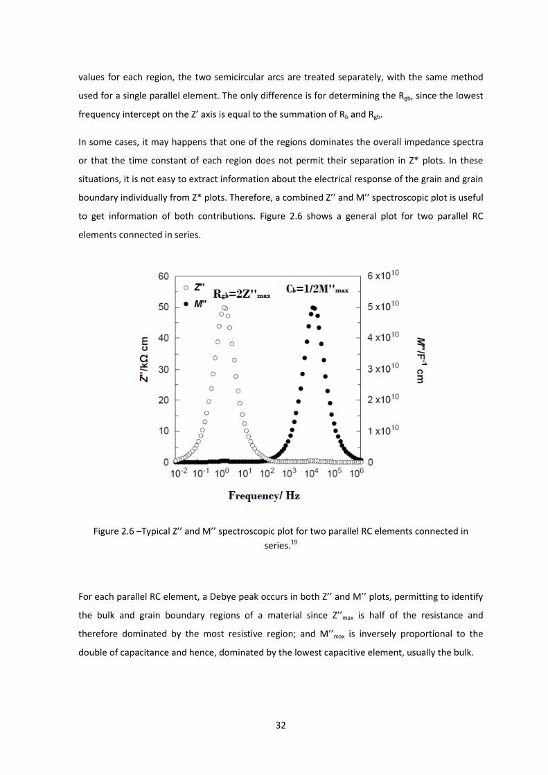
In some cases, it may happens that one of the regions dominates the overall impedance spectra
or that the time constant of each region does not permit their separation in Z* plots. In these
situations, it is not easy to extract information about the electrical response of the grain and grain
boundary individually from Z* plots. Therefore, a combined Z’’ and M’’ spectroscopic plot is useful
to get information of both contributions. Figure 2.6 shows a general plot for two parallel RC
elements connected in series.
Figure 2.6 –Typical Z’’ and M’’ spectroscopic plot for two parallel RC elements connected in
series.19
For each parallel RC element, a Debye peak occurs in both Z’’ and M’’ plots, permitting to identify
the bulk and grain boundary regions of a material since Z’’max is half of the resistance and
therefore dominated by the most resistive region; and M’’max is inversely proportional to the
double of capacitance and hence, dominated by the lowest capacitive element, usually the bulk.
33
2.4.2.7. The Brickwork Layer Model 44 ,45
The Brickwork Layer Model (BLM) is a model developed to interpret the IS spectra in materials
where the grain boundary is electrically resistive and the bulk semiconducting. BLM assumes
grains having cubic shape and perfect contacts between them, surrounded by identical thin
resistive grain boundary layers in all of the ceramic. Although the BLM is considered an
appropriate model to describe the electrical response of a material, some limitations are
associated because these assumptions in practice are not respected. A very important
consideration must be taken into account and is related to the values of resistance and
capacitance of the regions within the material. When the electrical properties of samples are
measured, the geometric factor, L/A (cm-1) where L is the thickness and A the lateral area of the
electrode, is applied to account for the effects of sample geometry and to obtain the relevant
material properties (i.e. resistivity and permittivity). However, the geometric factor is a
macroscopic value and, therefore, the specific resistivity and permittivity of the grain boundary
vary significantly from the values determined, giving rise to much higher apparent permittivity
Cgb(L/A) and lower resistivity Rgb(A/L) than they actual are. The capacitance and resistivity for bulk
can be considered a good approximation since the grains comprise the majority of the sample,
except possibly for nanomaterials.
2.4.2.8. Arrhenius plots
Arrhenius plots are useful to determine the activation energy of conduction, Ea, of a material. The
comparison of Ea within the same material allows to identificate if the conduction mechanism is
the same, for example, when samples of the same material are subjected to different processing.
It may also assists the interpretation of different microstructural contributions ascribed to internal
or external interfaces, etc. The conductivity of a material is thermally activated where it usually
obeys the Arrhenius equation:
(21)
34
where σ is the conductivity, σ0 is a pre-exponential factor, k is the Boltzmann constant
(1,38x10-23.J K-1) and T is the absolute temperature. Ea is found from the linear slope when log(σ)
is plotted against 1000/T.
2.5. Microstructural characterisation
In order to analyse the chemical evolution of CCTO ceramics with sintering process, a pellet
sintered at 1100 oC was analyzed by scanning electron microscopy (SEM) using a JEOL 6400 and a
backscattered electron image (BEI) was performed to identify the presence of any secondary
phases. The chemical composition was also analyzed by energy-dispersive X-ray spectroscopy
(EDS).
The pellet was ground and then polished with diamond paste down to 1 µm. Carbon coating was
used..as..conducting..surface..to..avoid..charging..under..the..electron..beam.
3. Results and discussion
In this chapter, the results of the experimental work are shown and a brief discussion as they are
presented is performed. Subsequently, an extensive discussion is done. The chapter is divided into
two sections: the first presents a composition and microstructure characterisation of the CCTO
compound. The second section approaches the electrical properties characterisation by
impedance spectroscopy of the samples to evaluate the effect of the high-energy ball milling and
sintering temperature on the electrical properties of CCTO ceramics.
To simpifly the identification of samples, they are denominated as shown in the table below with
the respective relative density.
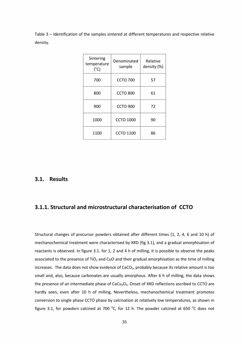
35
Table 3 – Identification of the samples sintered at different temperatures and respective relative
density.
3.1. Results
3.1.1. Structural and microstructural characterisation of CCTO
Structural changes of precursor powders obtained after different times (1, 2, 4, 6 and 10 h) of
mechanochemical treatment were characterised by XRD (fig 3.1), and a gradual amorphisation of
reactants is observed. In figure 3.1. for 1, 2 and 4 h of milling, it is possible to observe the peaks
associated to the presence of TiO2 and CuO and their gradual amorphisation as the time of milling
increases. The data does not show evidence of CaCO3, probably because its relative amount is too
small and, also, because carbonates are usually amorphous. After 6 h of milling, the data shows
the presence of an intermediate phase of CaCu2O3. Onset of XRD reflections ascribed to CCTO are
hardly seen, even after 10 h of milling. Nevertheless, mechanochemical treatment promotes
conversion to single phase CCTO phase by calcination at relatively low temperatures, as shown in
figure 3.1, for powders calcined at 700 oC, for 12 h. The powder calcined at 650 oC does not
Sintering temperature
(oC)
Denominated sample
Relative density (%)
700 CCTO 700 57
800 CCTO 800 61
900 CCTO 900 72
1000 CCTO 1000 90
1100 CCTO 1100 86
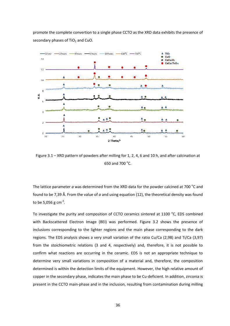
36
promote the complete convertion to a single phase CCTO as the XRD data exhibits the presence of
secondary phases of TiO2 and CuO.
Figure 3.1 – XRD pattern of powders after milling for 1, 2, 4, 6 and 10 h, and after calcination at
650 and 700 oC.
The lattice parameter a was determined from the XRD data for the powder calcined at 700 oC and
found to be 7,39 Å. From the value of a and using equation (12), the theoretical density was found
to be 5,056 g cm-3.
To investigate the purity and composition of CCTO ceramics sintered at 1100 oC, EDS combined
with Backscattered Electron Image (BEI) was performed. Figure 3.2 shows the presence of
inclusions corresponding to the lighter regions and the main phase corresponding to the dark
regions. The EDS analysis shows a very small variation of the ratio Cu/Ca (2,98) and Ti/Ca (3,97)
from the stoichiometric relations (3 and 4, respectively) and, therefore, it is not possible to
confirm what reactions are occurring in the ceramic. EDS is not an appropriate technique to
determine very small variations in composition of a material and, therefore, the composition
determined is within the detection limits of the equipment. However, the high relative amount of
copper in the secondary phase, indicates the main phase to be Cu-deficient. In addition, zirconia is
present in the CCTO main-phase and in the inclusion, resulting from contamination during milling
o o
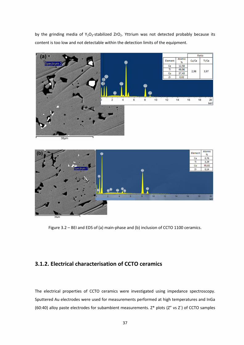
37
by the grinding media of Y2O3-stabilized ZrO2. Yttrium was not detected probably because its
content is too low and not detectable within the detection limits of the equipment.
Figure 3.2 – BEI and EDS of (a) main-phase and (b) inclusion of CCTO 1100 ceramics.
3.1.2. Electrical characterisation of CCTO ceramics
The electrical properties of CCTO ceramics were investigated using impedance spectroscopy.
Sputtered Au electrodes were used for measurements performed at high temperatures and InGa
(60:40) alloy paste electrodes for subambient measurements. Z* plots (Z” vs Z´) of CCTO samples
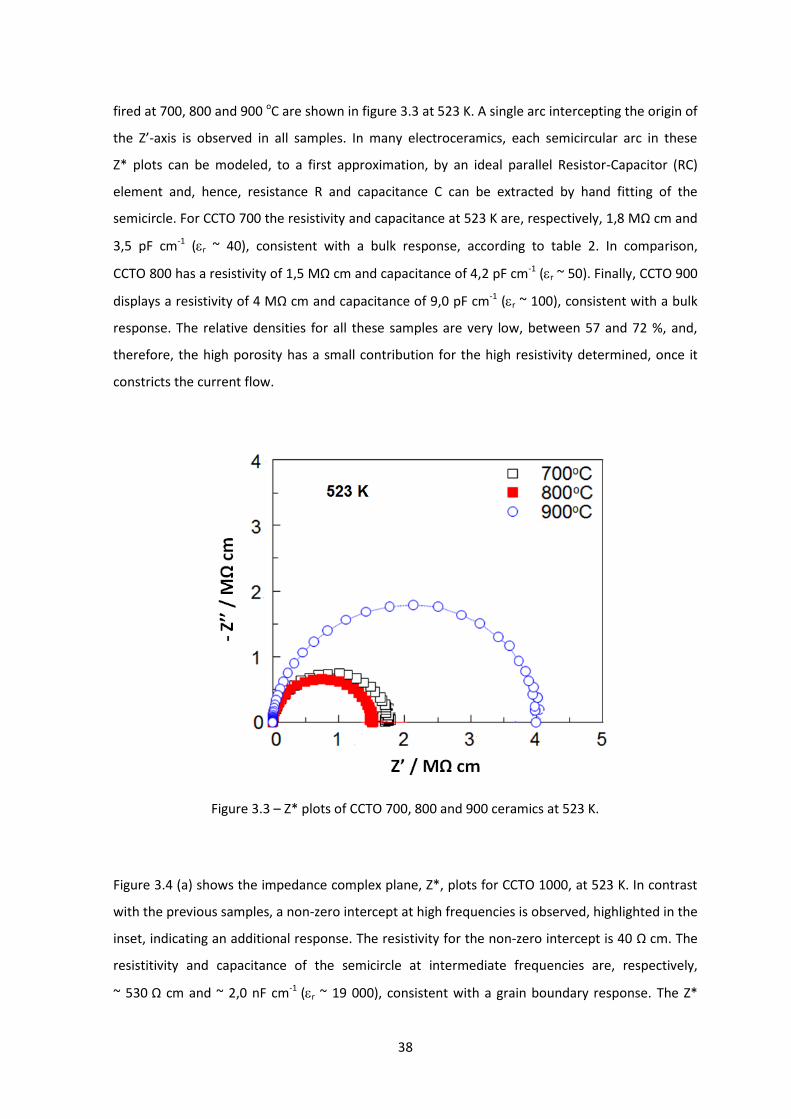
38
fired at 700, 800 and 900 oC are shown in figure 3.3 at 523 K. A single arc intercepting the origin of
the Z’-axis is observed in all samples. In many electroceramics, each semicircular arc in these
Z* plots can be modeled, to a first approximation, by an ideal parallel Resistor-Capacitor (RC)
element and, hence, resistance R and capacitance C can be extracted by hand fitting of the
semicircle. For CCTO 700 the resistivity and capacitance at 523 K are, respectively, 1,8 MΩ cm and
3,5 pF cm-1 (r ~ 40), consistent with a bulk response, according to table 2. In comparison,
CCTO.800 has a resistivity of 1,5 MΩ cm and capacitance of 4,2 pF cm-1 (r ~ 50). Finally, CCTO 900
displays a resistivity of 4 MΩ cm and capacitance of 9,0 pF cm-1 (r ~ 100), consistent with a bulk
response. The relative densities for all these samples are very low, between 57 and 72 %, and,
therefore, the high porosity has a small contribution for the high resistivity determined, once it
constricts the current flow.
Figure 3.3 – Z* plots of CCTO 700, 800 and 900 ceramics at 523 K.
Figure 3.4 (a) shows the impedance complex plane, Z*, plots for CCTO 1000, at 523 K. In contrast
with the previous samples, a non-zero intercept at high frequencies is observed, highlighted in the
inset, indicating an additional response. The resistivity for the non-zero intercept is 40 Ω cm. The
resistitivity and capacitance of the semicircle at intermediate frequencies are, respectively,
~ 530.Ω cm and ~ 2,0 nF cm-1 (r ~ 19 000), consistent with a grain boundary response. The Z*
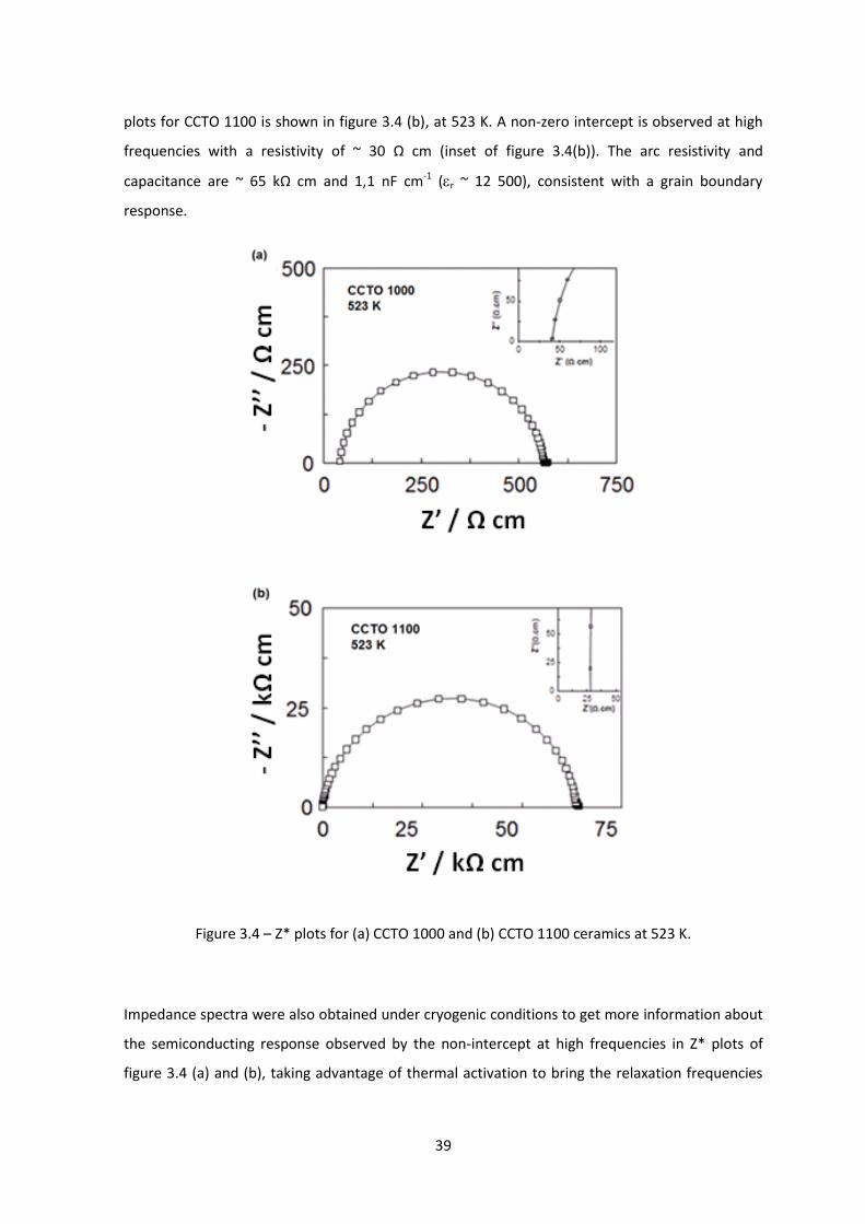
39
plots for CCTO 1100 is shown in figure 3.4 (b), at 523 K. A non-zero intercept is observed at high
frequencies with a resistivity of ~ 30 Ω cm (inset of figure 3.4(b)). The arc resistivity and
capacitance are ~ 65 kΩ cm and 1,1 nF cm-1 (r ~ 12 500), consistent with a grain boundary
response.
Figure 3.4 – Z* plots for (a) CCTO 1000 and (b) CCTO 1100 ceramics at 523 K.
Impedance spectra were also obtained under cryogenic conditions to get more information about
the semiconducting response observed by the non-intercept at high frequencies in Z* plots of
figure 3.4 (a) and (b), taking advantage of thermal activation to bring the relaxation frequencies
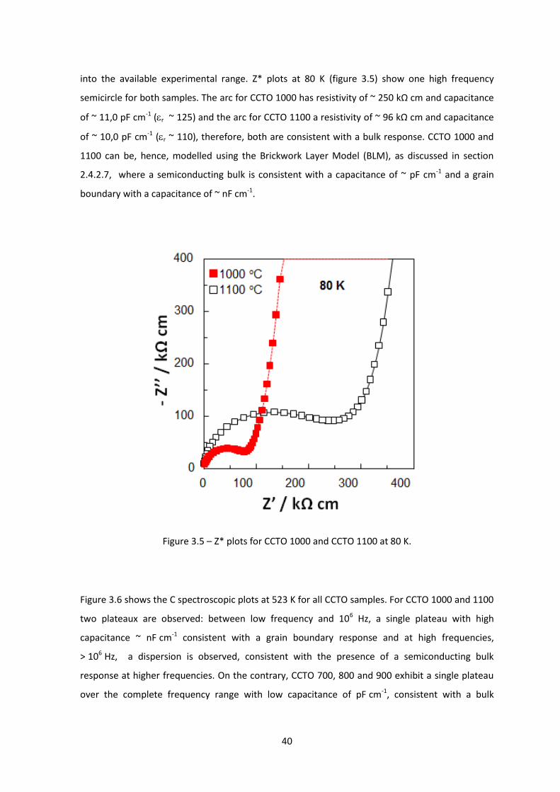
40
into the available experimental range. Z* plots at 80 K (figure 3.5) show one high frequency
semicircle for both samples. The arc for CCTO 1000 has resistivity of ~ 250 kΩ cm and capacitance
of ~ 11,0 pF cm-1 (r ~ 125) and the arc for CCTO 1100 a resistivity of ~ 96 kΩ cm and capacitance
of ~ 10,0 pF cm-1 (r ~ 110), therefore, both are consistent with a bulk response. CCTO 1000 and
1100 can be, hence, modelled using the Brickwork Layer Model (BLM), as discussed in section
2.4.2.7, where a semiconducting bulk is consistent with a capacitance of ~ pF cm-1 and a grain
boundary with a capacitance of ~ nF cm-1.
Figure 3.5 – Z* plots for CCTO 1000 and CCTO 1100 at 80 K.
Figure 3.6 shows the C spectroscopic plots at 523 K for all CCTO samples. For CCTO 1000 and 1100
two plateaux are observed: between low frequency and 106 Hz, a single plateau with high
capacitance ~ nF.cm-1 consistent with a grain boundary response and at high frequencies,
>.106.Hz, a dispersion is observed, consistent with the presence of a semiconducting bulk
response at higher frequencies. On the contrary, CCTO 700, 800 and 900 exhibit a single plateau
over the complete frequency range with low capacitance of pF.cm-1, consistent with a bulk
41
response. The grain boundary response does not appear in the all temperature range as the
samples have very low relative density, between 57 and 72.%, and therefore the microstructure
consists only of grains.
Figure 3.6 – C spectroscopic plots for all samples at 523 K.
Figure 3.7 shows the C spectroscopic plot at 10, 100 and 320 K for CCTO 1000 and 1100. The
C.spectroscopic plot at subambient temperatures helps to identify and characterise the other
response observed at high frequencies in figure 3.4. Both samples show the same trend where at
320 K the high capacitance dominates almost all the frequency range.
At 100 K, both the low frequency grain boundary plateau and the high frequency bulk plateau are
visible, with the dispersion moved to intermediate frequencies. At 10,K the plateau is totally
dominated by the bulk as a low capacitance of ~ pF.cm-1 is observed. Grain boundary
capacitances, Cgb, of ~ 2,0 nF.cm-1 and ~ 0,9 nf.cm-1 for CCTO 1000 and 1100, respectively, were
obtained from the low frequency plateau at 320.K, whereas the bulk capacitances, Cb of
~.8,5.pF.cm-1 for both samples were obtained from the high frequency plateau at 10 K.
42
Figure 3.7 – C spectroscopic plots of (a) CCTO 1000 and (b) CCTO 1100 samples at 10, 100 and
320.K.
M’’ spectroscopic plots for CCTO 700, 800 and 900 at subambient temperatures are shown in
figure 3.8. M’’, electric modulus, spectroscopic plots provide information sometimes not readily
43
available from Z* plots and permit to assess, in this case, the electrical homogeneity and
temperature dependence of the bulk capacitance.
In IS, each parallel RC element results in a Debye peak in the M’’ spectroscopic plot, where C is
inversely to the double of M’’ maximum peak, M’’max, corresponding to the Debye-peak. The
Debye-peak is hence, dominated by the lowest capacitive component of a sample. CCTO 700 does
not exhibit any Debye-peak at subambient temperatures, and therefore the bulk is totally
resistive. The beginning of the peak at 320 K is due to a resistive grain response. However, when
compared with CCTO 800 and 900 a Debye-peak is observed in all temperatures measured. In
figure 3.8 (b) at 80 K, the presence of a Debye-peak at low frequencies, ~ 6 kHz, is observed and as
the temperature increases, the Debye-peak shifts towards higher frequencies. At 260 K, this peak
starts to disappear on the frequency window and another peak starts to appear at low
frequencies, shifting to higher frequencies with increasing temperature. This indicates the bulk to
consist in an inner semiconducting region surrounded by a resistive outer region. The first peak to
disappear at high temperatures corresponds to the semiconducting region and the second peak
to the resistive region. In figure 3.8 (c), the same trend is observed for CCTO 900 when compared
with CCTO 800, indicating the bulk to be electrically heterogeneous as well.
44
Figure 3.8 – M’’ spectroscopic plots for (a) CCTO 700, (b) for CCTO 800 and (c) for CCTO 900 at
subambient temperatures. The measurement temperatures are shown in the label.
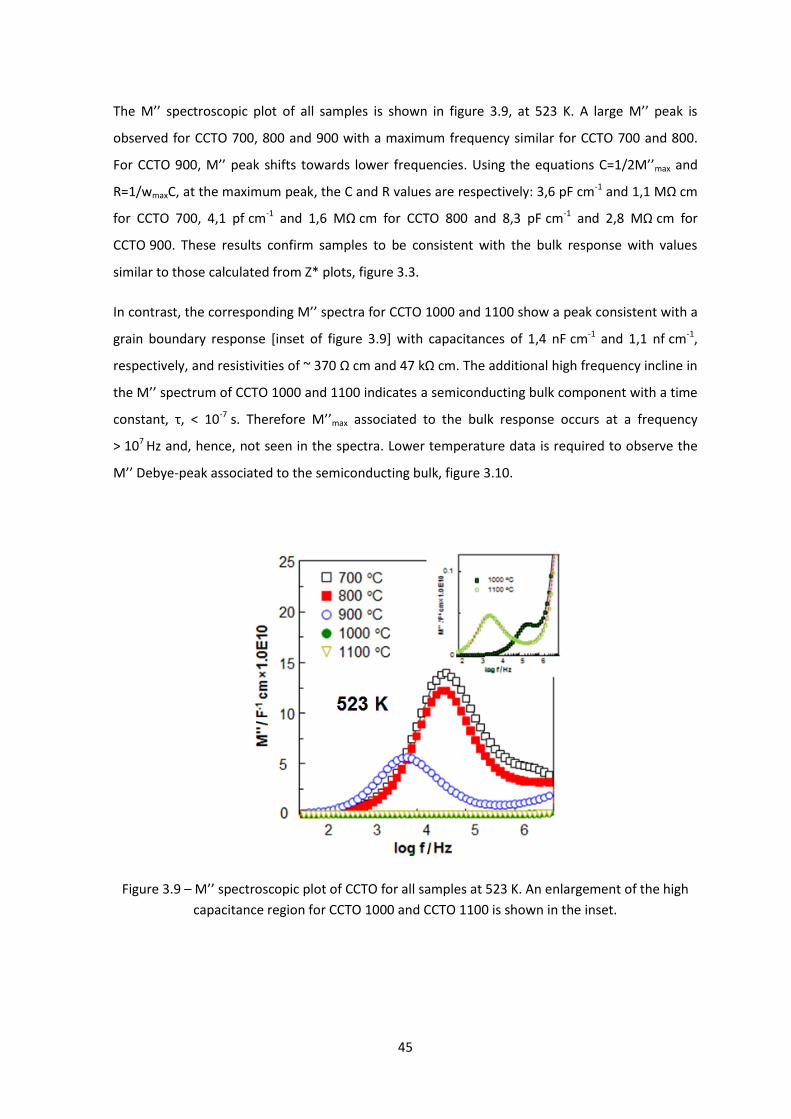
45
The M’’ spectroscopic plot of all samples is shown in figure 3.9, at 523 K. A large M’’ peak is
observed for CCTO 700, 800 and 900 with a maximum frequency similar for CCTO 700 and 800.
For CCTO 900, M’’ peak shifts towards lower frequencies. Using the equations C=1/2M’’max and
R=1/wmaxC, at the maximum peak, the C and R values are respectively: 3,6 pF cm-1 and 1,1 MΩ cm
for CCTO 700, 4,1 pf.cm-1 and 1,6 MΩ.cm for CCTO 800 and 8,3 pF.cm-1 and 2,8 MΩ.cm for
CCTO.900. These results confirm samples to be consistent with the bulk response with values
similar to those calculated from Z* plots, figure 3.3.
In contrast, the corresponding M’’ spectra for CCTO 1000 and 1100 show a peak consistent with a
grain boundary response [inset of figure 3.9] with capacitances of 1,4 nF.cm-1 and 1,1 nf.cm-1,
respectively, and resistivities of ~ 370 Ω cm and 47 kΩ cm. The additional high frequency incline in
the M’’ spectrum of CCTO 1000 and 1100 indicates a semiconducting bulk component with a time
constant, τ, < 10-7.s. Therefore M’’max associated to the bulk response occurs at a frequency
>.107.Hz and, hence, not seen in the spectra. Lower temperature data is required to observe the
M’’ Debye-peak associated to the semiconducting bulk, figure 3.10.
Figure 3.9 – M’’ spectroscopic plot of CCTO for all samples at 523 K. An enlargement of the high
capacitance region for CCTO 1000 and CCTO 1100 is shown in the inset.
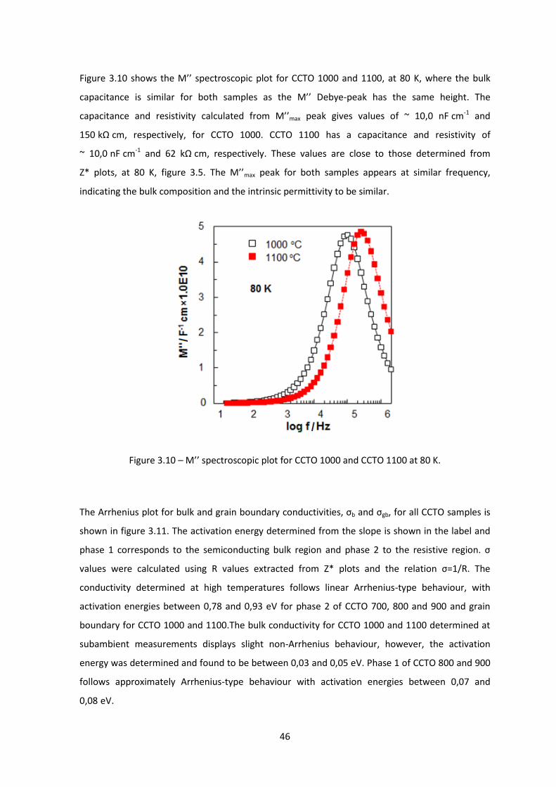
46
Figure 3.10 shows the M’’ spectroscopic plot for CCTO 1000 and 1100, at 80 K, where the bulk
capacitance is similar for both samples as the M’’ Debye-peak has the same height. The
capacitance and resistivity calculated from M’’max peak gives values of ~ 10,0 nF.cm-1 and
150.kΩ.cm, respectively, for CCTO 1000. CCTO 1100 has a capacitance and resistivity of
~ 10,0.nF.cm-1 and 62 kΩ.cm, respectively. These values are close to those determined from
Z* plots, at 80 K, figure 3.5. The M’’max peak for both samples appears at similar frequency,
indicating the bulk composition and the intrinsic permittivity to be similar.
Figure 3.10 – M’’ spectroscopic plot for CCTO 1000 and CCTO 1100 at 80 K.
The Arrhenius plot for bulk and grain boundary conductivities, σb and σgb, for all CCTO samples is
shown in figure 3.11. The activation energy determined from the slope is shown in the label and
phase 1 corresponds to the semiconducting bulk region and phase 2 to the resistive region. σ
values were calculated using R values extracted from Z* plots and the relation σ=1/R. The
conductivity determined at high temperatures follows linear Arrhenius-type behaviour, with
activation energies between 0,78 and 0,93 eV for phase 2 of CCTO 700, 800 and 900 and grain
boundary for CCTO 1000 and 1100.The bulk conductivity for CCTO 1000 and 1100 determined at
subambient measurements displays slight non-Arrhenius behaviour, however, the activation
energy was determined and found to be between 0,03 and 0,05 eV. Phase 1 of CCTO 800 and 900
follows approximately Arrhenius-type behaviour with activation energies between 0,07 and
0,08.eV.
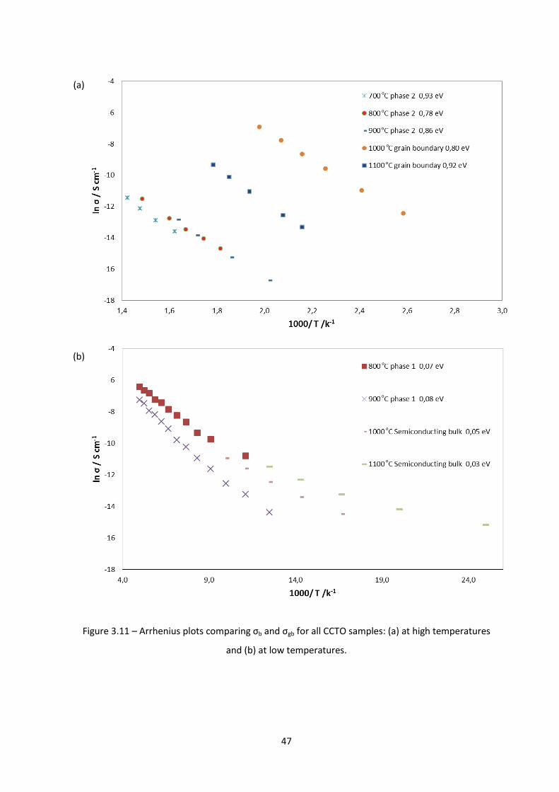
47
Figure 3.11 – Arrhenius plots comparing σb and σgb for all CCTO samples: (a) at high temperatures
and (b) at low temperatures.
(a)
(b)
o
o
o
o
o
o
o
o
o

48
To assess the variation of composition of CCTO, the fmax plot is shown in figure 3.12. fmax
corresponds to the frequency of the Debye-peak in the M’’ spectroscopic plots and permits
comparison of the composition between samples of the same material. Figure 3.12, shows the
composition change for the bulk and grain boundary of CCTO ceramics. In the label, phase 1 is
related to the semiconducting bulk region and phase 2 to the resistive bulk region. The curves
related to the phase 2 for CCTO 700, 800 and 900 are overlaid, indicating the composition of the
resistive bulk region to be similar. The composition for phase 1 of CCTO 800 and 900 is also
similar. The semiconducting bulk for CCTO 1000 and 1100 is similar, however, different from the
phase 1 for CCTO 800 and 900. In addition, the curve for the bulk of CCTO 1000 and 1100 shifts
towards lower temperatures, indicating the bulk to become more conducting compared to the
phase 1 of CCTO 800 and 900. The grain boundary composition changes from CCTO 1000 to
CCTO.1100, where it becomes more resistive.
Figure 3.12 – Representation of the maximum frequency of M’’max peak with temperature for all
samples.
o
o
o
o
o
o
o
o
o
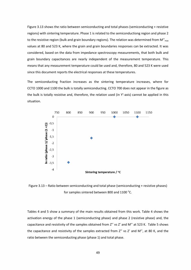
49
Figure 3.13 shows the ratio between semiconducting and total phases (semiconducting + resistive
regions) with sintering temperature. Phase 1 is related to the semiconductiong region and phase 2
to the resistive region (bulk and grain boundary regions). The relation was determined from M’’max
values at 80 and 523 K, where the grain and grain boundaries responses can be extracted. It was
considered, based on the data from impedance spectroscopy measurements, that both bulk and
grain boundary capacitances are nearly independent of the measurement temperature. This
means that any measurement temperature could be used and, therefore, 80 and 523 K were used
since this document reports the electrical responses at these temperatures.
The semiconducting fraction increases as the sintering temperature increases, where for
CCTO.1000 and 1100 the bulk is totally semiconducting. CCTO 700 does not appear in the figure as
the bulk is totally resistive and, therefore, the relation used (in Y’-axis) cannot be applied in this
situation.
Figure 3.13 – Ratio between semiconducting and total phase (semiconducting + resistive phases)
for samples sintered between 800 and 1100 oC.
Tables 4 and 5 show a summary of the main results obtained from this work. Table 4 shows the
activation energy of the phase 1 (semiconducting phase) and phase 2 (resistive phase) and, the
capacitance and resistivity of the samples obtained from Z’’ vs Z’ and M’’ at 523 K. Table 5 shows
the capacitance and resistivity of the samples extracted from Z’’ vs Z’ and M’’, at 80 K, and the
ratio between the semiconducting phase (phase 1) and total phase.
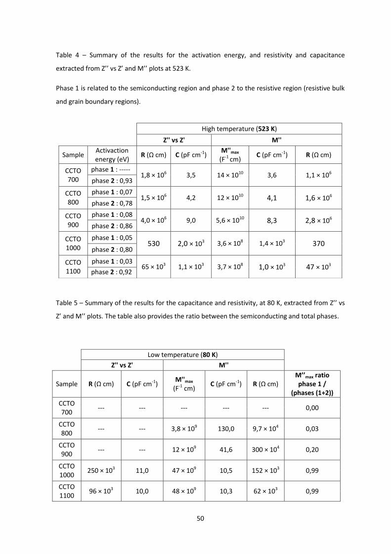
50
Table 4 – Summary of the results for the activation energy, and resistivity and capacitance
extracted from Z’’ vs Z’ and M’’ plots at 523 K.
Phase 1 is related to the semiconducting region and phase 2 to the resistive region (resistive bulk
and grain boundary regions).
Table 5 – Summary of the results for the capacitance and resistivity, at 80 K, extracted from Z’’ vs
Z’ and M’’ plots. The table also provides the ratio between the semiconducting and total phases.
High temperature (523 K)
Z'' vs Z' M''
Sample Activaction energy (eV)
R (Ω cm) C (pF cm-1) M''max
(F-1.cm) C (pF cm-1) R (Ω cm)
CCTO 700
phase 1 : ----- 1,8 × 10⁶ 3,5 14 × 1010 3,6 1,1 × 10⁶
phase 2 : 0,93
CCTO 800
phase 1 : 0,07 1,5 × 10⁶ 4,2 12 × 1010 4,1 1,6 × 10⁶
phase 2 : 0,78
CCTO 900
phase 1 : 0,08 4,0 × 10⁶ 9,0 5,6 × 10¹⁰ 8,3 2,8 × 10⁶
phase 2 : 0,86
CCTO 1000
phase 1 : 0,05 530 2,0 × 10³ 3,6 × 10⁸ 1,4 × 10³ 370
phase 2 : 0,80
CCTO 1100
phase 1 : 0,03 65 × 103 1,1 × 10³ 3,7 × 10⁸ 1,0 × 10³ 47 × 103
phase 2 : 0,92
Low temperature (80 K)
Z'' vs Z' M''
Sample R (Ω cm) C (pF cm-1) M''max
(F-1 cm) C (pF cm-1) R (Ω cm)
M’’max ratio phase 1 /
(phases (1+2))
CCTO 700
--- --- --- --- --- 0,00
CCTO 800
--- --- 3,8 × 10⁹ 130,0 9,7 × 10⁴ 0,03
CCTO 900
--- --- 12 × 109 41,6 300 × 104 0,20
CCTO 1000
250 × 103 11,0 47 × 109 10,5 152 × 103 0,99
CCTO 1100
96 × 103 10,0 48 × 109 10,3 62 × 103 0,99
51
3.2. Discussion
Powders were shown to be single phase CCTO, by X-ray diffraction, when calcined at 700.oC,
indicating the high-energy ball milling to be successful in the production of single-phase CCTO at
lower temperatures when compared to the conventional solid state reaction (950.-.1100.oC). At
the calcination temperature of 650 oC, secondary phases are still present.
A secondary phase was detected in ceramics sintered at 1100 oC and the chemical analysis
showed this phase to be Cu-rich and, therefore, the main phase is Cu-deficient. This change in the
composition of CCTO ceramics contributes to the increase of the bulk semiconductivity. The
detection of zirconia in the CCTO phase resulted from the contamination of the grinding media
used during milling and it may also affects the electrical properties of CCTO ceramics.
CCTO 700 ceramics exhibit resistive bulk with resistivity of ~ 1,8 MΩ cm at 523 K obtained from
Z* plots and confirmed by M’’ spectroscopic plot (fig. 3.3) by the absence of any Debye-peak at
subambient temperatures. The capacitance of ~ 3,5 pF.cm-1 confirms the response to be due to
the bulk region. Contrary to what is reported in the literature for CCTO ceramics, an IBLC electrical
microstructure is not present as the bulk is resistive and a single plateau is observed in the
C spectroscopic plot, figure 3.6. CCTO 700 behaves as an insulator and the ceramic has low
relative density, 57 %.
CCTO 800 and 900 also exhibit, in Z* plots at 523 K, (figure 3.3) an absence of a non-zero intercept
in Z´-axis, suggesting the bulk to be resistive. The bulk resistivity, at 523 K, for these two samples
are 1,5 and 4 MΩ.cm and the capacitance 3,2 and 9,0 pF.cm-1, respectively. The C plateau in figure
3.6 also confirms the data to be related to the bulk response. However, M’’ spectroscopic plots,
figure 3.8 (a), for CCTO 800 show at 260 K two Debye-peaks: the high frequency peak corresponds
to a semiconducting bulk region and the low frequency is related to a resistive bulk region. This
indicates the bulk to be electrically heterogeneous consisting in an inner semiconducting core
surrounded by a resistive region. The same trend can be observed for CCTO 900 and the ratio
between semiconducting and total region (figure 3.13) of the bulk increases with the sintering
temperature.
In contrast, CCTO 1000 and CCTO 1100 display an IBLC microstructure, similar to that of CCTO
ceramics found in the literature. Using IS, the grain boundary resistivity, at 523 K, is ~ 530 Ω.cm
52
and bulk resistivity ~ 40 Ω.cm for CCTO 1000. For CCTO 1100, the grain boundary and bulk
resistivity are, respectively, ~ 65 kΩ cm and ~ 30 Ω cm. Comparing CCTO 1000 and 1100, the bulk
resistivity is similar, however, a substantial difference is seen for the grain boundary resistivity:
CCTO 1100 grain boundary resistivity is almost 2 orders of magnitude greater than CCTO 1000.
This may be attributed to the presence of a reoxidized grain boundary composition favored at
higher temperatures of sintering. The ratio between semiconducting and total phase of the bulk,
figure 3.13, confirms the bulk to be totally semiconducting. To confirm the non-intercept
response in Z’-axis of Z* plots for CCTO 1000 and 1100, an additional Z* plots at lower
temperature, at 80 K, is shown in figure 3.5, where the capacitance of ~ 10,0 pF.cm-1 for both
samples confirms that the low resistivity at high frequencies observed in Z* plots at 523.K is
related to the bulk component. The IBLC mechanism starts to emerge, therefore, at the sintering
temperature of 800 oC and increases as the sintering temperature increases.
In the Z* plots at 80.K, Rb is ~ 250 and 96 kΩ.cm for CCTO 1000 and CCTO 1100, respectively.
Analysis of the Z* plots for these two samples at low temperatures is required, where the
resistivity of the semiconducting bulk becomes high enough to be observable within the
frequency range of measurement, Hz.-.MHz, and the electrical response characterised.
The σb and σgb for all samples is shown in Arrhenius plot format in figure 3.11. σb of sample
CCTO.700 and phase 2 (resistive region) of CCTO 800 and 900 is very similar and follows linear
Arrhenius- type behaviour. The activation energy is between 0,78 and 0,93 eV, suggesting similar
bulk composition. On the other hand, the activation energy is similar to that observed for the
grain boundary for CCTO 1000 and 1100, indicating the mechanism of conduction to be similar.
σgb of CCTO 1000 and 1100 are higher compared with the resistive bulk of CCTO 700, 800 and 900.
CCTO 1000 σgb is higher compared to CCTO 1100, which is in accordance with Z* plots at 523.K,
figure 3.4.
The bulk conductivity of phase 1 in CCTO 800, CCTO 900, CCTO 1000 and CCTO 1100, measured at
subambient temperatures, displays slight non-Arrhenius behaviour and, therefore, the activation
energy determined is not so accurate. However, the bulk of CCTO 1100 is more conducting than
CCTO 1000, showing that higher sintering temperatures contribute to a higher decomposition of
the CCTO bulk ceramics.
The C spectroscopic plot, figure 3.6, shows for CCTO 700, 800 and 900, a single and frequency
independent plateau response. The capacitances obtained from C spectroscopic plot are,
respectively, 4,0.pF.cm-1 for both CCTO 700 and 800, and 9,0 pF cm-1 for CCTO 900, giving values
53
of permittivity approximately 40 and 110, consistent with the values obtained from Z* plots. In
contrast with the results available in the literature, the ‘giant’ permittivity for undoped CCTO does
not appear in these samples.
For CCTO 1000 and 1100, the high capacitance at low frequencies is consistent with a grain
boundary response and, at high frequencies, the dispersion of capacitance is related to the
semiconducting bulk and this is in accordance with the information displayed in the literature,
where two different responses are observed in C spectroscopic plots. Although and as mentioned
before in section 2.4.2.7., it is not possible to calculate accurately the capacitance of the grain
boundary, however, from the low frequency plateau is possible to determine the gb capacitances
of 2 and 1.nF cm-1, giving rise to the permittivities of ~ 18 000 and 11 300, for CCTO 1000 and
1100. The ‘giant’ permittivity appears, therefore, for CCTO 1000 and 1100 samples and, it seems
associated with the presence of a thin and reoxidized grain boundary region on the outer surfaces
of the semiconducting grain.
Interestingly, CCTO 1000 capacitance is higher compared to that of CCTO 1100 sample. According
to equation (4), larger grains result in higher effective permittivity whereas the grain boundary
thickness and intrinsic permittivity are usually assumed to be constant. According to the
fundaments of sintering, when the sintering temperature rises, it usually gives rise to larger grains
and, therefore, it would be expected the effective permittivity of CCTO 1100 to be higher. The
justification should, therefore, focus on the effective permittivity and/or grain boundary which
may change with the processing conditions.
54
4. Conclusion
Pure phase CaCu3Ti4O12 was synthesized at lower temperature by high-energy ball milling. X-ray
diffraction revealed that pure phase CCTO powders can be obtained on calcination at 700.oC for
12 hours. At the calcination temperature of 650 oC, the presence of secondary phases of TiO2 and
CuO are observed on XRD data.
From the microstructure study on CCTO 1100 sample, the main-phase is Cu-deficient and this
contributed towards the increasing of the bulk conductivity in CCTO. However, the mechanism
responsible for the origin of the bulk semiconductivity is not well understood yet, but it may be
associated to the diffusion and eventual volatililisation of copper at elevated temperatures of
processing.
Impedance spectroscopy measurements showed different electrical microstructures for the
sintered pellets. CCTO 700 is an insulator with low relative density (57 %) and with a bulk
resistivity > 1 MΩ.cm. CCTO 800 and 900 are composed of semiconducting inner grains
surrounded by insulating outer grain regions. The grains have become totally semiconducting
when the sintering temperature increased to 1000 oC. IS results show, therefore, a general picture
about the evolution of the IBLC mechanism in CCTO ceramics with sintering temperature where
the conducting phase emerges and grows from the core part of grains at the expense of phase R.
The conducting phase exhibits resistivity < 100 Ω.cm, at 523 K. The volume fraction of resistive
phase in the grains decrease until it becomes a resistive thin layer corresponding to the grain
boundary region, for samples sintered at 1100.oC. The change in the resistivity of the phases
seems to be influenced by Cu-loss mechanism that may diffuse within grains towards grain
boundaries at elevated temperatures. The resistive phase CCTO can be prepared at low
temperatures by high-energy ball milling where the Cu-loss mechanism is suppressed as shown by
the absence of any peak in M’’ spectroscopic plot for samples sintered at 700 oC. However, the
high temperature required to get dense CCTO ceramics promotes the Cu-loss and, therefore, the
grains become semiconducting. The IBLC mechanism starts to appear when the sintering
temperature reaches 800 oC and its effect gets higher as the sintering temperature increases and
it is responsible for the ‘giant’ permittivity observed for CCTO 1000 and 1100, where the bulk is
completely semiconducting.
55
5. Future Work
To date there have been no transport studies on low temperature sintered CCTO ceramics that
primarily consist of insulating phase and therefore the type of charge carrier in it is unknow. The
conduction mechanisms in insulating phase and even in semiconducting phase remain unclear at
this stage. Further studies on the pO2 dependence of the conductivity of insulating phase in
ceramics in combination with Thermoelectric power measurements, Transmission Electron
Microscopy (TEM) and Electron Energy Loss spectroscopy (EELS) measurements need to be done
to resolve the conduction mechanisms in CCTO ceramics.
56
References
1. Cross, L. E., Newnham, R. E. History of Ferroelectrics. Journal of the American Ceramic
Society, 111, 1987.
2. Wang, H. L. Structure and Dielectric Properties of Perovskite. University of San Jose State,
2002.
3. Homes, C. C., Vogt, T., Shapiro, S. M., Wakimoto, S., Ramirez, A. P. Optical response of
high-dielectric-constant perovskite-related oxide. Science (New York), 293, 673, 2001.
4. Subramanian, M. A., Li, D., Duan, N., Reiner, B. A., Sleight, A. W. High Dielectric Constant in
ACu3Ti4O12 and ACu3Ti3FeO12 Phases. Solid State Chemistry, 151, 323–325, 2000.
5. Ramirez, A. P., Subramanian, M. A., Gardel, M., Blumberg, M., Li, D., Vogt, T., Shapiro, S. M.
Giant dielectric constant response in a copper-titanate. Solid State Communications, 115,
217–220, 2000.
6. Wang, C. M., Kao, K. S., Lin, S. Y., Chen, Y. C., Weng, S.C. Processing and properties of
CaCu3Ti4O12 ceramics. Physics and Chemistry of Solids, 69, 608–610, 2008.
7. Ezhilvalavan, S., Tseng, T. Y. Progress in the developments of (Ba,Sr)TiO3 (BST) thin films for
Gigabit era DRAMs. Materials Chemistry and Physics, 65, 227–248, 2000.
8. Woodward, P. M. Octahedral Tilting in Perovskites - Geometrical Considerations. Acta
Crystallographica B, 53, 32–43, 1997.
9. Johnsson, M., Lemmens, P. Crystallography and Chemistry of Perovskites. University of
Stockholm, 2005.
10. Howard, C. J., Stokes, H. T. Structures and phase transitions in perovskites - a group-
theoretical approach. Acta Crystallographica A, 61, 93–111, 2005.
11. Howard, C. J., Stokes, H. T. Group-Theoretical Analysis of Octahedral Tilting in Perovskites.
Acta Crystallographica B, 54, 782-789, 1998.
12. Zhou, J.S., Goodenough, J. B. Intrinsic structural distortion in orthorhombic perovskite
oxides. Physical Review B, 77, 2–5, 2008.
13. Fierro, J. L. G., Pena, M.A. Chemical Structures and Performance of Perovskite Oxides.
American Chemical Society, 101, 1981-2017, 2001.
57
14. King, G., Woodward, P. M. Cation ordering in perovskites. Materials Chemistry, 20, 5785–
5796, 2010.
15. Bozin, E.S., Petkov, V., Barnes, P.W., Woodward, P.M., Vogt, T., Mahanti, S.D., Billinge,
S.J.L.Temperature dependent total scattering structural study of CaCu3Ti4O12. Journal of
Physics: Condensed Matter, 16, 5091-5102, 2004.
16. Barnes, P. W., Lufaso, M. W., Woodward, P. M. Structure determination of A2M3+TaO6 and
A2M3+NbO6 ordered perovskites: octahedral tilting and pseudosymmetry. Acta
Crystallographica, 62, 384–396, 2006.
17. Subramanian, M. A., Sleight, A. W. ACu3Ti4O12 and ACu3Ru4O12 perovskites : high dielectric
constants and valence degeneracy. Solid State Sciences, 4, 347–351, 2002.
18. Yuan, W. Investigation on the decomposable process and the secondary liquid phase effect
on the dielectric properties of CaCu3Ti4O12 ceramics. Physics D: Applied Physics, 42,
175401, 2009.
19. Ferrarelli, M. C., Sinclair, D. C., West, A. R. Structure-Composition-Property Relations in the
ACu3Ti4O12 Structure-type. University of Sheffield, 2008.
20. Vijatović, M. M., Bobić, J. D., Stojanović, B. D. History and Challenges of Barium Titanate:
Part II. Science of Sintering, 40, 235–244, 2008.
21. Vijatović, M. M., Bobić, J. D., Stojanović, B. D. History and Challenges of Barium Titanate :
Part I. Science of Sintering, 40, 155–165, 2008.
22. Callister, W.D. Materials Science and engineering An Introduction, 7th edition, 2006.
23. He, L., Neaton, J.B., Cohen, M. H. Vanderbilt, D. A first-principles study of the structure and
lattice dielectric response of CaCu3Ti4O12. Physics Review B, 65, 214112, 2002.
24. Leroy, W. A fundamental study of advanced metal / semiconductor contacts. University of
Wetenschappen, 2007.
25. Moulson, A.J., Herber, J.M. Electroceramics. 2th edition, 2003.
26. Lunkenheimer, P., Fichtl, R., Ebbinghaus, S. G., Loidl, A. Non-intrinsic origin of the Colossal
Dielectric Constants in CaCu3Ti4O12. Physics Review, 1, 19–22, 2004.
27. Adams, B. T. B., Sinclair, D. C., West, A. R. Giant Barrier Layer Capacitance Effects in
CaCu3Ti4O12 Ceramics. Advanced Materials, 14, 2001–2003, 2002.
58
28. Adams, T. B., Sinclair, D. C., West, A. R. Influence of Processing Conditions on the Electrical
Properties of CaCu3Ti4O12 Ceramics. Journal of the American Ceramic Society, 89, 3129–
3135, 2006.
29. Sinclair, D. C., Adams, T. B., Morrison, F. D., West, A. R. CaCu3Ti4O12: One-step internal
barrier layer capacitor. Applied Physics Letters, 80, 2153, 2002.
30. Kim, I.D., Rothschild, A., Tuller, H. L. Direct current bias effects on grain boundary Schottky
barriers in CaCu3Ti4O12. Applied Physics Letters, 88, 072902, 2006.
31. Chung, S. Y., Kim, I.D., Kang, S. J. L. Strong nonlinear current-voltage behaviour in
perovskite-derivative calcium copper titanate. Nature Materials, 3, 774–778, 2004.
32. Li, M., Feteira, A., Sinclair, D. C., West, A. R. Influence of Mn doping on the semiconducting
properties of CaCu3Ti4O12 ceramics. Applied Physics Letters, 88, 232903, 2006.
33. Belous, A., Ovchar, O., Valant, M., Krzmanc, M. Suvorov, D. Microwave composite
dielectrics based on magnesium titanates. Journal of European Ceramic Society, 27, 2963–
2966, 2007.
34. Bender, B. A., Pan, M. J. The effect of processing on the giant dielectric properties of
CaCu3Ti4O12. Materials Science and Engineering, 117, 339–347, 2005.
35. Yang, J., Shen, M., Fang, L. The electrode/sample contact effects on the dielectric
properties of the CaCu3Ti4O12 ceramic. Materials Letters, 59, 3990–3993, 2005.
36. Patterson, E. A., Kwon, S., Huang, C., Cann, D. P., Patterson, E. A. Effects of ZrO2 additions
on the dielectric properties of CaCu3Ti4O12. Applied Physics Letters, 182911, 10–13, 2005.
37. Feng, L., Tang, X., Yan, Y., Chen, X., Jiao, Z., Cao, G. Decrease of dielectric loss in
CaCu3Ti4O12 ceramics by La doping. Physics State Solids, 4, 22–24, 2006.
38. Varma, B. S. R., Prakash, B. S. Microstructural and dielectric properties of donor doped
(La3+) CaCu3Ti4O12 ceramics. Materials Science, 17, 899–907, 2006.
39. Chen, Y., Li, C. P., Chen, H., Chen, Y. One-dimensional nanomaterials synthesized using
high-energy ball milling and annealing process. Science and Technology of Advanced
Materials, 7, 839–846, 2006.
40. West, A. R., Sinclair, D. C., Hirose, N. Characterization of Electrical Materials, Especially
Ferroelectrics by Impedance Spectroscopy. Electroceramics, 1:1, 65–71, 1997.
41. Sinclair, D. C. Characterization of Electro-materials using ac Impedance Spectroscopy.
Cerámica y Vidrio, 34, 55–66, 1995.
59
42. Macdonald, J.R. Impedance Spectroscopy. Annals of Biomedical Engineering, 20, 289–305,
1992.
43. Irvine, J. T. S., Sinclair, D. C., West, A. R. Electroceramics: Characterization by Impedance
Spectroscopy. Advanced Materials, 2, 132–138, 1990.
44. Fleig, J. The influence of non-ideal microstructures on the analysis of grain boundary
impedances. Solid State Ionics, 131, 117–127, 2000.
45. Fleig, J., Maier, J. The impedance of ceramics with highly resistive grain boundaries: validity
and limits of the brick layer model. Journal of European Ceramic Society, 19, 693–696,
1999.