Sanjay Banerjee, Ph.D. · Sanjay Banerjee is the Cockrell Family Regents Chair Professor of...
94
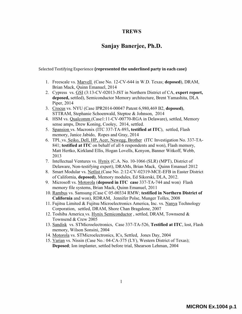
1 TREWS Sanjay Banerjee, Ph.D. Selected Testifying Experience (represented the underlined party in each case) 1. Freescale vs. Marvell (Case No. 12-CV-644 in W.D. Texas; deposed), DRAM, Brian Mack, Quinn Emanuel, 2014 2. Cypress vs. GSI (3:13-CV-02013-JST in Northern District of CA, expert report, deposed, settled), Semiconductor Memory architecture, Brent Yamashita, DLA Piper, 2014 3. Crocus vs. NYU (Case IPR2014-00047 Patent 6,980,469 B2, deposed), STTRAM, Stephanie Schoenwald, Steptoe & Johnson, 2014 4. HSM vs. Qualcomm (Case1:11-CV-00770-RGA in Delaware), settled, Memory sense amps, Drew Koning, Cooley, 2014, settled. 5. Spansion vs. Macronix (ITC 337-TA-893, testified at ITC), settled, Flash memory, Janice Jabido, Ropes and Gray, 2014 6. TPL vs. Seiko, Dell, HP, Acer, Newegg, Brother (ITC Investigation No. 337-TA- 841; testified at ITC on behalf of all 6 respondents and won), Flash memory, Matt Hertko, Kirkland Ellis, Hogan Lovells, Kenyon, Banner Witkoff, Webb, 2013 7. Intellectual Ventures vs. Hynix (C.A. No. 10-1066 (SLR) (MPT), District of Delaware, Non-testifying expert), DRAMs, Brian Mack, Quinn Emanuel 2012 8. Smart Modular vs. Netlist (Case No. 2:12-CV-02319-MCE-EFB in Easter District of California, deposed), Memory modules, Ed Sikorski, DLA, 2012. 9. Microsoft vs. Motorola (deposed in ITC case 337-TA-744 and won) Flash memory file systems, Brian Mack, Quinn Emanuel, 2011 10. Rambus vs. Samsung (Case C 05-00334 RMW; testified in Northern District of California and won), RDRAM, Jennifer Polse, Munger Tolles, 2008 11. Fujitsu Limited & Fujitsu Microelectronics America, Inc. vs. Nanya Technology Corporation, settled, DRAM, Shore Chan Bragalone, 2007 12. Toshiba America vs. Hynix Semiconductor , settled, DRAM, Townsend & Townsend & Crew 2005 13. Sandisk vs. STMicroelectronics, Case 337-TA-526, Testified at ITC, lost, Flash memory, Wilson Sonsini, 2004 14. Motorola vs. STMicroelectronics, ICs, Settled, Jones Day, 2004 15. Varian vs. Nissin (Case No.: 04-CA-375 (LY), Western District of Texas); Deposed; Ion implanter, settled before trial, Shearson Lehman, 2004 MICRON Ex.1004 p.1
Transcript of Sanjay Banerjee, Ph.D. · Sanjay Banerjee is the Cockrell Family Regents Chair Professor of...
1
TREWS
Sanjay Banerjee, Ph.D.
Selected Testifying Experience (represented the underlined party in each case)
1. Freescale vs. Marvell (Case No. 12-CV-644 in W.D. Texas; deposed), DRAM,
Brian Mack, Quinn Emanuel, 2014
2. Cypress vs. GSI (3:13-CV-02013-JST in Northern District of CA, expert report,
deposed, settled), Semiconductor Memory architecture, Brent Yamashita, DLA
Piper, 2014
3. Crocus vs. NYU (Case IPR2014-00047 Patent 6,980,469 B2, deposed),
STTRAM, Stephanie Schoenwald, Steptoe & Johnson, 2014
4. HSM vs. Qualcomm (Case1:11-CV-00770-RGA in Delaware), settled, Memory
sense amps, Drew Koning, Cooley, 2014, settled.
5. Spansion vs. Macronix (ITC 337-TA-893, testified at ITC), settled, Flash
memory, Janice Jabido, Ropes and Gray, 2014
6. TPL vs. Seiko, Dell, HP, Acer, Newegg, Brother (ITC Investigation No. 337-TA-
841; testified at ITC on behalf of all 6 respondents and won), Flash memory,
Matt Hertko, Kirkland Ellis, Hogan Lovells, Kenyon, Banner Witkoff, Webb,
2013
7. Intellectual Ventures vs. Hynix (C.A. No. 10-1066 (SLR) (MPT), District of
Delaware, Non-testifying expert), DRAMs, Brian Mack, Quinn Emanuel 2012
8. Smart Modular vs. Netlist (Case No. 2:12-CV-02319-MCE-EFB in Easter District
of California, deposed), Memory modules, Ed Sikorski, DLA, 2012.
9. Microsoft vs. Motorola (deposed in ITC case 337-TA-744 and won) Flash
memory file systems, Brian Mack, Quinn Emanuel, 2011
10. Rambus vs. Samsung (Case C 05-00334 RMW; testified in Northern District of
California and won), RDRAM, Jennifer Polse, Munger Tolles, 2008
11. Fujitsu Limited & Fujitsu Microelectronics America, Inc. vs. Nanya Technology
Corporation, settled, DRAM, Shore Chan Bragalone, 2007
12. Toshiba America vs. Hynix Semiconductor , settled, DRAM, Townsend &
Townsend & Crew 2005
13. Sandisk vs. STMicroelectronics, Case 337-TA-526, Testified at ITC, lost, Flash
memory, Wilson Sonsini, 2004
14. Motorola vs. STMicroelectronics, ICs, Settled, Jones Day, 2004
15. Varian vs. Nissin (Case No.: 04-CA-375 (LY), Western District of Texas);
Deposed; Ion implanter, settled before trial, Shearson Lehman, 2004
MICRON Ex.1004 p.1
2
Sanjay Banerjee is the Cockrell Family Regents Chair Professor of Electrical and Computer
Engineering and Director, Microelectronics Research Center, at the University of Texas at Austin.
He is also the Director of the South West Academy of Nanoelectronics, one of three centers in the
US to develop a replacement for MOSFETs. He received his B.Tech from the Indian Institute of
Technology, Kharagpur, and his M.S. and Ph.D. from the University of Illinois at Urbana-
Champaign in 1979, 1981 and 1983 respectively, all in electrical engineering. As a Member of the
Technical Staff, Corporate Research, Development and Engineering of Texas Instruments
Incorporated from 1983-1987, he worked on polysilicon transistors and dynamic random access
trench memory cells used by Texas Instruments in the world's first 4Megabit DRAM. He has been
Assistant Professor (1987-90), Associate Professor (1990-93), and Professor (1993-) at The
University of Texas at Austin. He has over 1000 archival refereed publications/talks, 10
books/chapters, and 30 U.S. patents, and has supervised over 60 Ph.D. and 70 MS students. His
students have received 10 Best Papers Awards at various conferences, and he has presented over
100 invited talks. He received the Engineering Foundation Advisory Council Halliburton Award,
1991, the Texas Atomic Energy Fellowship (1990-1997), Cullen Professorship (1997-2001) and
the Hocott Research Award from UT Austin (2007). He has won the IEEE Grove Award (2014),
Distinguished Alumnus Award, IIT (2005), Industrial R&D 100 Award (2004), ECS Callinan
Award, 2003, IEEE Millennium Medal, 2000, NSF Presidential Young Investigator Award in
1988, and several SRC Inventor Recognition and Best Paper Awards. He was a Distinguished
Lecturer for IEEE Electron Devices Society, and the General Chair of the IEEE Device Research
Conference, 2002. He is a Fellow of IEEE, APS and AAAS. He is active in the areas of beyond-
CMOS nanoelectronic transistors based on 2D materials and spintronics, fabrication and modeling
of advanced MOSFETs, and solar cells.
MICRON Ex.1004 p.2
3
Sanjay Kumar Banerjee
Current Position: Cockrell Family Regents Chair in
Electrical and Computer Engineering, 1999-
Director, Microelectronics Research Center, 1999-
Education: University of Illinois, PhD (Electrical Engineering), 1983
University of Illinois, MS (Electrical Engineering), 1981
Indian Institute of Technology at Kharagpur, India, B. Tech (Electronics), 1979
Professional Engineer: Texas
Previous Positions: Cullen Trust Endowed Professorship in Engineering No.1, 1997-2001
University of Texas, Associate Director, Microelectronics Research Center, 1996-99
University of Texas, Professor, September 1993-
University of Texas, Associate Professor, September 1990- August 1993
University of Texas, Assistant Professor, September 1987- August, 1990
Texas Instruments, Corporate R& D, Member of Technical Staff, 1983-August 1987
Honors and Awards:
IEEE Andrew Grove Award (2014)
Fellow of American Association for Advancement of Science (2007)
Hocott Research Award, Univ. of Texas, 2007
Fellow, American Physical Society, 2006
Distinguished Alumnus Award, IIT, 2005
Industrial R&D 100 Award (with R.Singh) 2004
Electrochemical Society Thomas D. Callinan Award, 2003 Micron Professorship (2003- 10)
IEEE Millennium Medal, 2001
SRC Inventor Recognition Awards, 1994, 2000, 2009
Best Paper Awards, SRC 1998, 2006, 2009, 2010,2014, 2015
Who’s Who Listings (Marquis)
Cullen Professorship, Univ. of Texas, 1997- 2001
Distinguished Lecturer for the IEEE Electron Devices Society (1997-2003), Adcom
Member till 1998
Fellow of IEEE, 1996
Engineering Foundation Advisory Council Halliburton Award, 1991
Texas Atomic Energy Centennial Fellowship, 1990-97
NSF Presidential Young Investigator Award, 1988
Best Paper Award, IEEE International Solid State Circuits Conference, 1986
Jagadis Bose and National Science Talent Search Scholarships, India, 1974-79
Institute Medal and Swapan Saha Prize for Highest Ranking Undergraduate (ECE),
I.I.T., India, 1979
Phi Kappa Phi
MICRON Ex.1004 p.3
4
Professional Society and Major Government Committees:
Technical Advisory Board: Applied Novel Devices (current) AstroWatt, DSM Semiconductors,
Cambrios, Nanocoolers Inc., BeSang Memories, Organic ID and ITU Ventures;Gerson Lehmann
Group, NY; Austin Community College; Asia Pacific IIIT; Rochester Institute of Technology,
HSMC Foundry
IEEE Dan Noble Award Committee, 2010-13 (Chair, 2012-13)
Congressional round-table panel member on nanotechnology, Feb. 2008
Member on International Technology Roadmap for Semiconductors
Siemens Westinghouse Science Talent Contest Judge, 2003
Morgan & Claypool Publishers, Lectures in Electronic Materials &Devices, Series Editor
SISPAD, Program Committee, 2005-6
Electrochemical Society Symposium on SiGe, Program Committee, 2004
IRPS, Program Committee, 2005
12th Int. Workshop on Physics of Semiconductor Devices, Int. Advisory Committee
Int. Advisory Committee, Int. Conf. on MEMS and Nanotechnology, IIT, 2005
Program Committee, International SiGe Technology and Device Meeting, 2004-2012
IEEE Device Research Conference Technical Program Chair, 2000-01, General Chair, 2001-02
Editorial Board, Elsevier Science, 2001
IEDM Program Committee, Modeling and Simulation, Session Chair, 2001-03
ECS Session Chair, Toronto, Canada, May 2000
Program Committee, IEEE Int. Conf. Communications, Computers, Devices, Kharagpur, 2000.
IEEE Device Research Conference Program Committee/Local Arrangements Chair, 1999-2000
NSF Workshop Co-Organizer for “Front and Back-end Processes”, Austin, TX 1999
Eleventh Int. Ion Implant Tech. Meet. Program Committee and Publications Chair, 1995-1996.
IEEE Symposium on VLSI Technology, Committee Member, 1992-98
NSF Workshop Organizer for “Silicon-Germanium Devices”, Austin, TX 1999
IEEE University Government Industry Microelectronics Symp., General Chairman, 1994-1995
IEEE International Electron Devices Meeting, (Device Technology/ Session Chair: 1989-90)
IEEE Conf. on Electromagnetic Field Computation, Chair Comp. in Electron Dev., CA, 1992
Panel Member, SRC Conference on Integration of Novel Processes, 1991
Sponsored Research: Grant title: "Three-Dimensional IC Technology,"
Co-Principal Investigator:S.Banerjee
Other Investigators: D.L. Kwong
Sponsoring Agency: Texas Advanced Technology Program
Duration: June 1988-August 1990.
Grant title: "High Speed Devices and VLSI Structures by Laser-Enhanced Epitaxy,"
Principal Investigator: S.Banerjee
Sponsoring Agency: Texas Advanced Technology Program
Duration: June 1988-August 1990.
Grant title: "Optoelectronic Devices by Photo-enhanced Chemical Vapor Deposition,"
MICRON Ex.1004 p.4
5
Principal Investigator: S.Banerjee
Sponsoring Agency: National Science Foundation PYI
Duration: August 1988- July 1993.
Grant title: "GaAs-on-Si MESFET Modeling,"
Principal Investigator: S.Banerjee
Sponsoring Agency: Texas Instruments, Inc.
Duration: December 1988- August 1989.
Grant title: "Understanding and Modeling of Unit Processes"
Co-Investigator: S.Banerjee
Other Investigators: W.Adcock (PI), A.Tasch (Co-PI), I.Trachtenberg (Co-PI),
D.Kwong, J.Lee, T.Edgar and J.Ekerdt
Sponsoring Agency: SEMATECH and SRC
Duration: December 1988- August 1993.
Grant title: "RPCVD Epitaxial Silicon and Insulators for Use in 3-D CMOS Integrated
Circuits,"
Co-Investigator: S.Banerjee
Other Investigators: A.Tasch (P.I.), A.Cowley and R.Jones
Sponsoring Agency: Office of Naval Research
Duration: Sept. 1987- March 1990.
Grant title: "Ballistic and Quantum Transport in Si Devices at Cryogenic Temperatures"
Principal Investigator:S.Banerjee
Other Investigators: J.Lee
Sponsoring Agency: Texas Advanced Technology Program
Duration: November 1989- November 1991.
Grant title: "Polysilicon Transistor Modeling,"
Principal Investigator: S.Banerjee
Sponsoring Agency: Motorola
Duration: September, 1991-August, 1993.
Grant title: "Acquisition of High Resolution Transmission Electron Microscope,"
Principal Investigator: L.Rabenberg
Other Investigators: S.Banerjee, J.Goodenough, A.Heller, P.Ho and A.Manthiram
Sponsoring Agency: National Science Foundation
Duration: 10/92-10/93
Grant title: "Atomic Layer Epitaxy of Group IV Semiconductors,"
Co-Principal Investigator: S.Banerjee
Other Investigators: A.Tasch (P.I.), A.Cowley, J.Ekerdt and R.Jones
Sponsoring Agency: Office of Naval Research
Duration: February 1991-August 1996.
MICRON Ex.1004 p.5
6
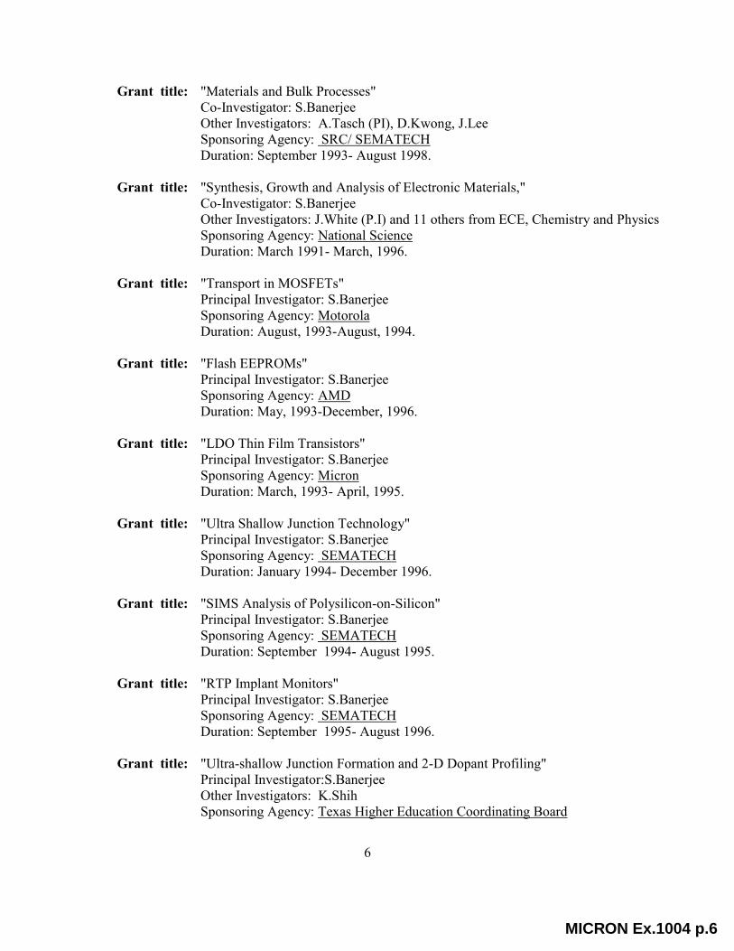
Grant title: "Materials and Bulk Processes"
Co-Investigator: S.Banerjee
Other Investigators: A.Tasch (PI), D.Kwong, J.Lee
Sponsoring Agency: SRC/ SEMATECH
Duration: September 1993- August 1998.
Grant title: "Synthesis, Growth and Analysis of Electronic Materials,"
Co-Investigator: S.Banerjee
Other Investigators: J.White (P.I) and 11 others from ECE, Chemistry and Physics
Sponsoring Agency: National Science
Duration: March 1991- March, 1996.
Grant title: "Transport in MOSFETs"
Principal Investigator: S.Banerjee
Sponsoring Agency: Motorola
Duration: August, 1993-August, 1994.
Grant title: "Flash EEPROMs"
Principal Investigator: S.Banerjee
Sponsoring Agency: AMD
Duration: May, 1993-December, 1996.
Grant title: "LDO Thin Film Transistors"
Principal Investigator: S.Banerjee
Sponsoring Agency: Micron
Duration: March, 1993- April, 1995.
Grant title: "Ultra Shallow Junction Technology"
Principal Investigator: S.Banerjee
Sponsoring Agency: SEMATECH
Duration: January 1994- December 1996.
Grant title: "SIMS Analysis of Polysilicon-on-Silicon"
Principal Investigator: S.Banerjee
Sponsoring Agency: SEMATECH
Duration: September 1994- August 1995.
Grant title: "RTP Implant Monitors"
Principal Investigator: S.Banerjee
Sponsoring Agency: SEMATECH
Duration: September 1995- August 1996.
Grant title: "Ultra-shallow Junction Formation and 2-D Dopant Profiling"
Principal Investigator:S.Banerjee
Other Investigators: K.Shih
Sponsoring Agency: Texas Higher Education Coordinating Board
MICRON Ex.1004 p.6
7
Duration: January 1996- December 1997.
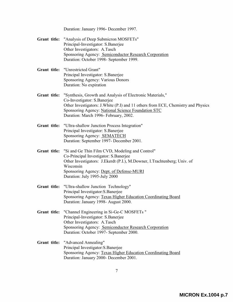
Grant title: "Analysis of Deep Submicron MOSFETs"
Principal-Investigator: S.Banerjee
Other Investigators: A.Tasch
Sponsoring Agency: Semiconductor Research Corporation
Duration: October 1998- September 1999.
Grant title: "Unrestricted Grant"
Principal Investigator: S.Banerjee
Sponsoring Agency: Various Donors
Duration: No expiration
Grant title: "Synthesis, Growth and Analysis of Electronic Materials,"
Co-Investigator: S.Banerjee
Other Investigators: J.White (P.I) and 11 others from ECE, Chemistry and Physics
Sponsoring Agency: National Science Foundation STC
Duration: March 1996- February, 2002.
Grant title: "Ultra-shallow Junction Process Integration"
Principal Investigator: S.Banerjee
Sponsoring Agency: SEMATECH
Duration: September 1997- December 2001.
Grant title: "Si and Ge Thin Film CVD, Modeling and Control"
Co-Principal Investigator: S.Banerjee
Other Investigators: J.Ekerdt (P.I.), M.Downer, I.Trachtenberg; Univ. of
Wisconsin
Sponsoring Agency: Dept. of Defense-MURI
Duration: July 1995-July 2000
Grant title: "Ultra-shallow Junction Technology"
Principal Investigator:S.Banerjee
Sponsoring Agency: Texas Higher Education Coordinating Board
Duration: January 1998- August 2000.
Grant title: "Channel Engineering in Si-Ge-C MOSFETs "
Principal-Investigator: S.Banerjee
Other Investigators: A.Tasch
Sponsoring Agency: Semiconductor Research Corporation
Duration: October 1997- September 2000.
Grant title: "Advanced Annealing"
Principal Investigator:S.Banerjee
Sponsoring Agency: Texas Higher Education Coordinating Board
Duration: January 2000- December 2001.
MICRON Ex.1004 p.7
8
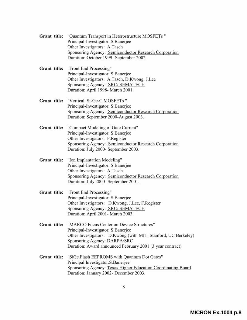
Grant title: "Quantum Transport in Heterostructure MOSFETs "
Principal-Investigator: S.Banerjee
Other Investigators: A.Tasch
Sponsoring Agency: Semiconductor Research Corporation
Duration: October 1999- September 2002.
Grant title: "Front End Processing"
Principal-Investigator: S.Banerjee
Other Investigators: A.Tasch, D.Kwong, J.Lee
Sponsoring Agency: SRC/ SEMATECH
Duration: April 1998- March 2001.
Grant title: "Vertical Si-Ge-C MOSFETs "
Principal-Investigator: S.Banerjee
Sponsoring Agency: Semiconductor Research Corporation
Duration: September 2000-August 2003.
Grant title: "Compact Modeling of Gate Current"
Principal-Investigator: S.Banerjee
Other Investigators: F.Register
Sponsoring Agency: Semiconductor Research Corporation
Duration: July 2000- September 2003.
Grant title: "Ion Implantation Modeling"
Principal-Investigator: S.Banerjee
Other Investigators: A.Tasch
Sponsoring Agency: Semiconductor Research Corporation
Duration: July 2000- September 2001.
Grant title: "Front End Processing"
Principal-Investigator: S.Banerjee
Other Investigators: D.Kwong, J.Lee, F.Register
Sponsoring Agency: SRC/ SEMATECH
Duration: April 2001- March 2003.
Grant title: "MARCO Focus Center on Device Structures"
Principal-Investigator: S.Banerjee
Other Investigators: D.Kwong (with MIT, Stanford, UC Berkeley)
Sponsoring Agency: DARPA/SRC
Duration: Award announced February 2001 (3 year contract)
Grant title: "SiGe Flash EEPROMS with Quantum Dot Gates"
Principal Investigator:S.Banerjee
Sponsoring Agency: Texas Higher Education Coordinating Board
Duration: January 2002- December 2003.
MICRON Ex.1004 p.8
9
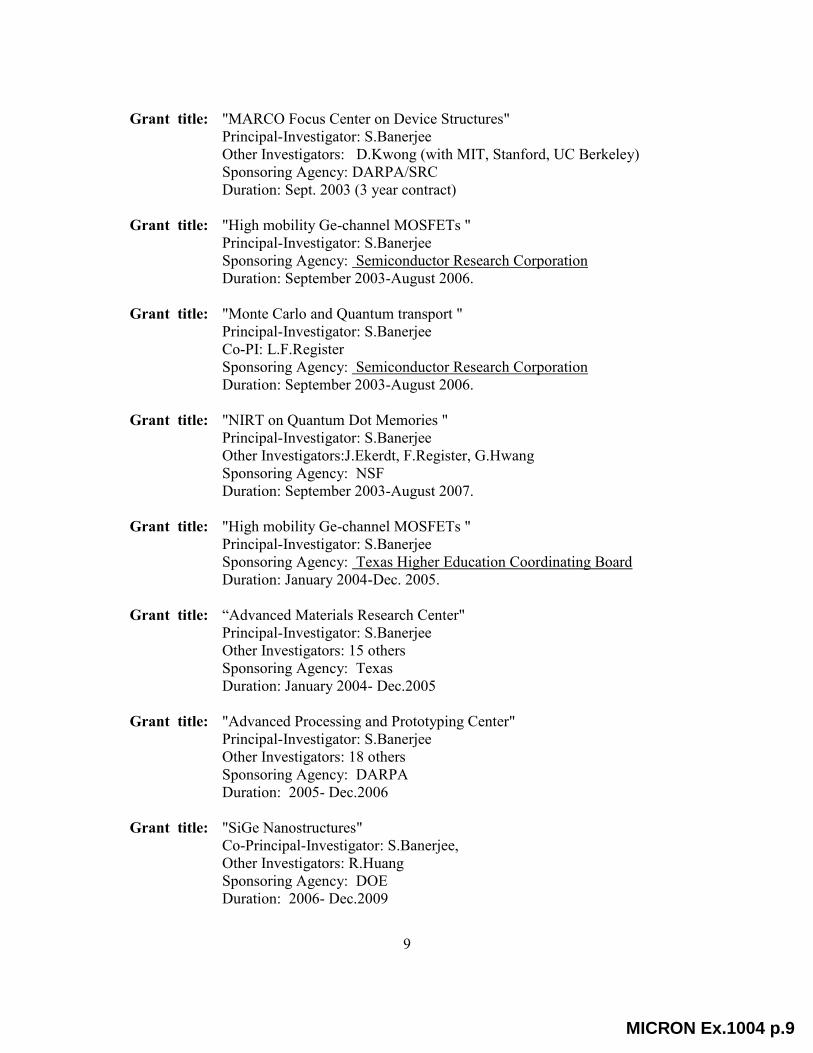
Grant title: "MARCO Focus Center on Device Structures"
Principal-Investigator: S.Banerjee
Other Investigators: D.Kwong (with MIT, Stanford, UC Berkeley)
Sponsoring Agency: DARPA/SRC
Duration: Sept. 2003 (3 year contract)
Grant title: "High mobility Ge-channel MOSFETs "
Principal-Investigator: S.Banerjee
Sponsoring Agency: Semiconductor Research Corporation
Duration: September 2003-August 2006.
Grant title: "Monte Carlo and Quantum transport "
Principal-Investigator: S.Banerjee
Co-PI: L.F.Register
Sponsoring Agency: Semiconductor Research Corporation
Duration: September 2003-August 2006.
Grant title: "NIRT on Quantum Dot Memories "
Principal-Investigator: S.Banerjee
Other Investigators:J.Ekerdt, F.Register, G.Hwang
Sponsoring Agency: NSF
Duration: September 2003-August 2007.
Grant title: "High mobility Ge-channel MOSFETs "
Principal-Investigator: S.Banerjee
Sponsoring Agency: Texas Higher Education Coordinating Board
Duration: January 2004-Dec. 2005.
Grant title: “Advanced Materials Research Center"
Principal-Investigator: S.Banerjee
Other Investigators: 15 others
Sponsoring Agency: Texas
Duration: January 2004- Dec.2005
Grant title: "Advanced Processing and Prototyping Center"
Principal-Investigator: S.Banerjee
Other Investigators: 18 others
Sponsoring Agency: DARPA
Duration: 2005- Dec.2006
Grant title: "SiGe Nanostructures"
Co-Principal-Investigator: S.Banerjee,
Other Investigators: R.Huang
Sponsoring Agency: DOE
Duration: 2006- Dec.2009
MICRON Ex.1004 p.9
10
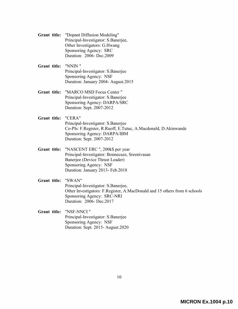
Grant title: "Dopant Diffusion Modeling"
Principal-Investigator: S.Banerjee,
Other Investigators: G.Hwang
Sponsoring Agency: SRC
Duration: 2006- Dec.2009
Grant title: "NNIN "
Principal-Investigator: S.Banerjee
Sponsoring Agency: NSF
Duration: January 2004- August.2015
Grant title: "MARCO MSD Focus Center "
Principal-Investigator: S.Banerjee
Sponsoring Agency: DARPA/SRC
Duration: Sept. 2007-2012
Grant title: "CERA"
Principal-Investigator: S.Banerjee
Co-PIs: F.Register, R.Ruoff, E.Tutuc, A.Macdonald, D.Akinwande
Sponsoring Agency: DARPA/IBM
Duration: Sept. 2007-2012
Grant title: "NASCENT ERC ", 200k$ per year
Principal-Investigator: Bonnecaze, Sreenivasan
Banerjee (Device Thrust Leader)
Sponsoring Agency: NSF
Duration: January 2013- Feb.2018
Grant title: "SWAN"
Principal-Investigator: S.Banerjee,
Other Investigators: F.Register, A.MacDonald and 15 others from 6 schools
Sponsoring Agency: SRC-NRI
Duration: 2006- Dec.2017
Grant title: "NSF-NNCI "
Principal-Investigator: S.Banerjee
Sponsoring Agency: NSF
Duration: Sept. 2015- August.2020
MICRON Ex.1004 p.10
11
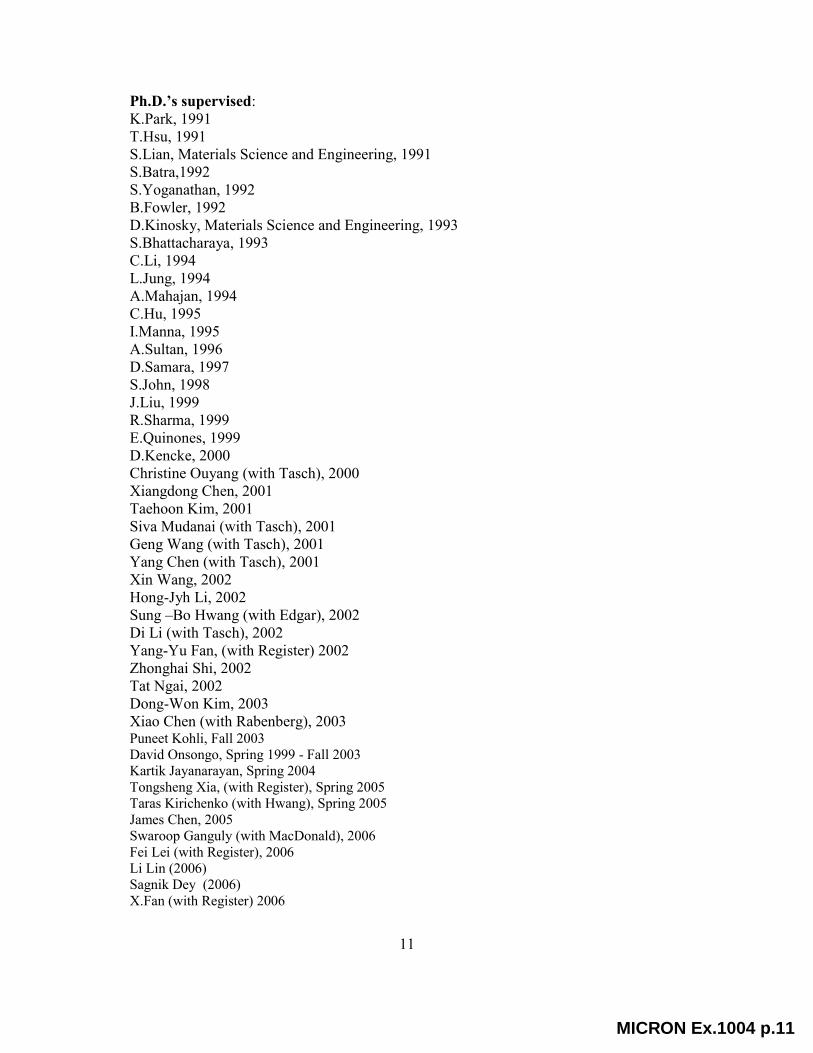
Ph.D.’s supervised:
K.Park, 1991
T.Hsu, 1991
S.Lian, Materials Science and Engineering, 1991
S.Batra,1992
S.Yoganathan, 1992
B.Fowler, 1992
D.Kinosky, Materials Science and Engineering, 1993
S.Bhattacharaya, 1993
C.Li, 1994
L.Jung, 1994
A.Mahajan, 1994
C.Hu, 1995
I.Manna, 1995
A.Sultan, 1996
D.Samara, 1997
S.John, 1998
J.Liu, 1999
R.Sharma, 1999
E.Quinones, 1999
D.Kencke, 2000
Christine Ouyang (with Tasch), 2000
Xiangdong Chen, 2001
Taehoon Kim, 2001
Siva Mudanai (with Tasch), 2001
Geng Wang (with Tasch), 2001
Yang Chen (with Tasch), 2001
Xin Wang, 2002
Hong-Jyh Li, 2002
Sung –Bo Hwang (with Edgar), 2002
Di Li (with Tasch), 2002
Yang-Yu Fan, (with Register) 2002
Zhonghai Shi, 2002
Tat Ngai, 2002
Dong-Won Kim, 2003
Xiao Chen (with Rabenberg), 2003 Puneet Kohli, Fall 2003
David Onsongo, Spring 1999 - Fall 2003 Kartik Jayanarayan, Spring 2004
Tongsheng Xia, (with Register), Spring 2005
Taras Kirichenko (with Hwang), Spring 2005
James Chen, 2005
Swaroop Ganguly (with MacDonald), 2006
Fei Lei (with Register), 2006
Li Lin (2006)
Sagnik Dey (2006)
X.Fan (with Register) 2006
MICRON Ex.1004 p.11
12
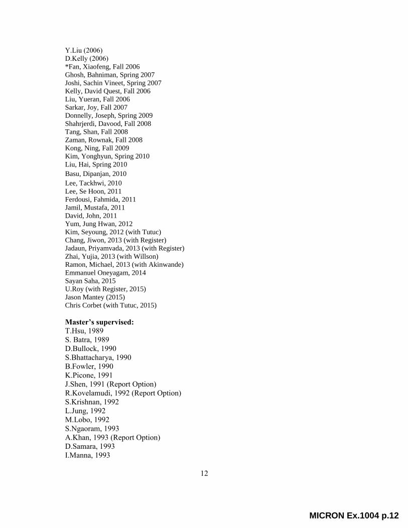
Y.Liu (2006)
D.Kelly (2006) *Fan, Xiaofeng, Fall 2006
Ghosh, Bahniman, Spring 2007
Joshi, Sachin Vineet, Spring 2007
Kelly, David Quest, Fall 2006
Liu, Yueran, Fall 2006
Sarkar, Joy, Fall 2007
Donnelly, Joseph, Spring 2009
Shahrjerdi, Davood, Fall 2008
Tang, Shan, Fall 2008
Zaman, Rownak, Fall 2008
Kong, Ning, Fall 2009
Kim, Yonghyun, Spring 2010
Liu, Hai, Spring 2010
Basu, Dipanjan, 2010
Lee, Tackhwi, 2010
Lee, Se Hoon, 2011
Ferdousi, Fahmida, 2011
Jamil, Mustafa, 2011
David, John, 2011
Yum, Jung Hwan, 2012
Kim, Seyoung, 2012 (with Tutuc)
Chang, Jiwon, 2013 (with Register)
Jadaun, Priyamvada, 2013 (with Register)
Zhai, Yujia, 2013 (with Willson)
Ramon, Michael, 2013 (with Akinwande)
Emmanuel Oneyagam, 2014
Sayan Saha, 2015
U.Roy (with Register, 2015)
Jason Mantey (2015)
Chris Corbet (with Tutuc, 2015)
Master’s supervised: T.Hsu, 1989
S. Batra, 1989
D.Bullock, 1990
S.Bhattacharya, 1990
B.Fowler, 1990
K.Picone, 1991
J.Shen, 1991 (Report Option)
R.Kovelamudi, 1992 (Report Option)
S.Krishnan, 1992
L.Jung, 1992
M.Lobo, 1992
S.Ngaoram, 1993
A.Khan, 1993 (Report Option)
D.Samara, 1993
I.Manna, 1993
MICRON Ex.1004 p.12
13
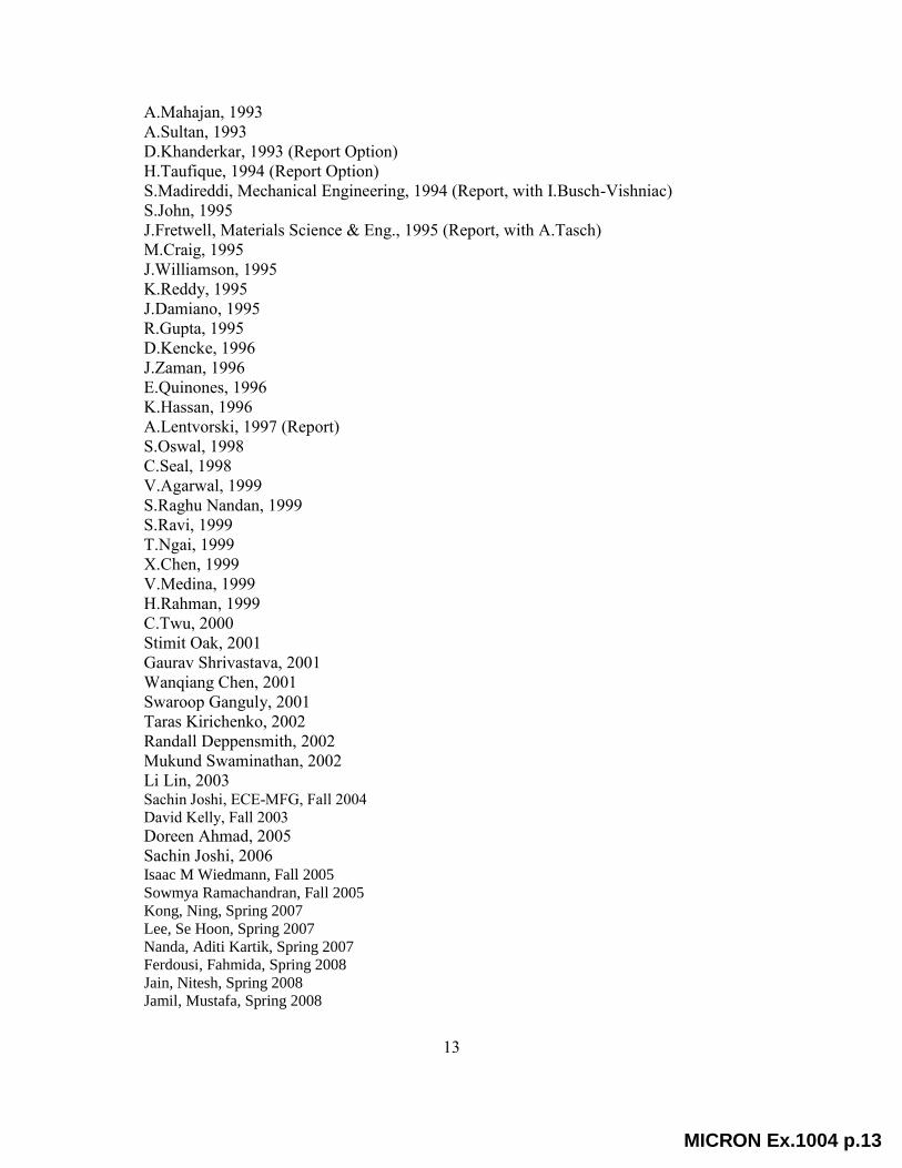
A.Mahajan, 1993
A.Sultan, 1993
D.Khanderkar, 1993 (Report Option)
H.Taufique, 1994 (Report Option)
S.Madireddi, Mechanical Engineering, 1994 (Report, with I.Busch-Vishniac)
S.John, 1995
J.Fretwell, Materials Science & Eng., 1995 (Report, with A.Tasch)
M.Craig, 1995
J.Williamson, 1995
K.Reddy, 1995
J.Damiano, 1995
R.Gupta, 1995
D.Kencke, 1996
J.Zaman, 1996
E.Quinones, 1996
K.Hassan, 1996
A.Lentvorski, 1997 (Report)
S.Oswal, 1998
C.Seal, 1998
V.Agarwal, 1999
S.Raghu Nandan, 1999
S.Ravi, 1999
T.Ngai, 1999
X.Chen, 1999
V.Medina, 1999
H.Rahman, 1999
C.Twu, 2000
Stimit Oak, 2001
Gaurav Shrivastava, 2001
Wanqiang Chen, 2001
Swaroop Ganguly, 2001
Taras Kirichenko, 2002
Randall Deppensmith, 2002
Mukund Swaminathan, 2002
Li Lin, 2003 Sachin Joshi, ECE-MFG, Fall 2004 David Kelly, Fall 2003
Doreen Ahmad, 2005 Sachin Joshi, 2006 Isaac M Wiedmann, Fall 2005
Sowmya Ramachandran, Fall 2005
Kong, Ning, Spring 2007
Lee, Se Hoon, Spring 2007
Nanda, Aditi Kartik, Spring 2007
Ferdousi, Fahmida, Spring 2008
Jain, Nitesh, Spring 2008
Jamil, Mustafa, Spring 2008
MICRON Ex.1004 p.13
14
Jayan, Baby Reeja, Spring 2008
Kim, Seyoung, Summer 2008
Onyegam, Emmanuel U., Fall 2007
Vora, Nikhil Sudhir, Spring 2008
Chang, Jiwon, Spring 2009
Jadaun, Priyamvada, Summer 2009
Varahramyan, Kamran, Fall 2008
Kaur, Shagandeep, Spring 2010
Zhai, Yu-Jia, Spring 2010
Saha, Sayan, 2010
Rik Dey, 2014
Nima, Asoudegi, 2015
Postdocs: Samit Ray, Mark Loewe, Amitava Das, Sabrina Grannan, Freek Prins, W.C.Jung,
M.Palard, C.Mao, Bhagawan Sahu, Mathew Gilbert, J.Lee, D.Ahn, Domingo Ferrer, Samaraesh
Gucchait, Aparna Gupta, Anupam Roy, Sushant Sonde, Sarmita Majumdar, Bahniman Ghosh,
Rudy Ghosh
In progress:
Corbet, Christopher
Mantey, Jason
Onyegam, Emmanuel
Ramon, Michael
Hema Chandra Mova
Yu-jia Zhai
Urmimala Roy
Nima Assoudeghi
William Hsu
Dax Crum
Sangwoo Kang
MICRON Ex.1004 p.14
15
Books and Invited Book Chapters: 1. Solid State Electronic Devices, 5th Ed. (2000), 6th Ed. (2005), 7th Ed. (2015), Prentice-Hall by
B.Streetman and S.Banerjee
2. Effect of Surface Nitridation on the Electrical Characteristics of Germanium High-κ/Metal Gate
Metal-Oxide-Semiconductor Devices, D. Q. Kelly, J. J.-H. Chen, S. Guha, and S. K. Banerjee.
Invited Book chapter, Springer, 2007.
3. SiGe HFETs, S.Banerjee, The Silicon Heterostructure Handbook, 2005, Edited by John
Cressler.
4. High-k Gate Dielectrics, Y.Fan. S.Mudanai, L. Register and S.Banerjee, 2003
5. Device Miniaturization and Simulation, S.Banerjee and B.Streetman in ULSI Devices, John
Wiley, 2000 (C.Chang and S.Sze editors)
6. Dopant Diffusion, S.Banerjee in Handbook of Semiconductor Manufacturing Technology,
Marcel Dekker, 2000, 2006 (Y.Nishi, B.Doering and J.Kilby editors).
7. Silicon-germanium Devices, S.Banerjee, Elsevier, 2001.
8. Novel 3D CMOS, S.Dey and S.Banerjee, Solid State Electronics Trends, 2009
9. X. Mou, L. F. Register and S. K. Banerjee, “Ultra-low-power pseudospintronics devices
via exciton condensation in coupled two-dimensional material systems,” in Nanoscale
Materials and Devices for Electronics, Photonics and Solar Energy, Ed. Stephen Goodnick,
Anatoli Korkin and Robert Nemanich, Springer, 2015
10. D. Reddy, L. F. Register and S. K. Banerjee, "Bilayer pseudoSpin Field Effect
Transistor (BiSFET)" in "Beyond CMOS Logic Switches," T.-J. King and K. Kuhn, Eds.,
Cambridge: Cambridge Univ. Press, 2015.
Patents:
United States Patent 8188460, 2012
Bi-layer pseudo-spin field-effect transistor
United States Patent 8,198,707, 2012 Establishing a uniformly thin dielectric layer on graphene in a semiconductor device
without affecting the properties of graphene
United States Patent 8,008,649, 2011
Incorporating gate control over a resonant tunneling structure in CMOS to reduce off-
state current leakage, supply voltage and power consumption
US Patent 6,744,083, 2004
Submicron MOSFET having asymmetric channel profile
US Patent 6,420,219, 2002
Thin film transistor and method
US06320202
Bottom gated thin film transistors comprising Ge in a channel region
US06,319,799, 11/20/2001
High mobility heterojunction transistor and method
MICRON Ex.1004 p.15
16
US06,313,486, 11/06/2001
Floating gate transistor having silicon germanium channel layer
US06,313,487, 11/06/2001
Vertical channel floating gate transistor having SiGe channel layer
US06214652
Thin film transistor and method of forming thin film transistors
US06,200,839
Methods of making thin film transistors
US06166398 12/26/2000 Thin film transistors
US06017782 01/25/2000 Thin film transistor and method of forming thin film transistors
US05985703 11/16/1999 Method of making thin film transistors
US05977560 11/02/1999
Thin film transistor constructions with polycrystalline silicon-germanium alloy doped with carbon
in the channel region
US05953596 09/14/1999
Methods of forming thin film transistors
US05936262 08/10/1999 Thin film transistors
US05904513 05/18/1999 Method of forming thin film transistors
US05665981 09/09/1997
Thin film transistors and method of promoting large crystal grain size in the formation of
polycrystalline silicon alloy thin films
US05548132 08/20/1996
Thin film transistor with large grain size DRW offset region and small grain size source and drain
and channel regions
US05546340 08/13/1996
Non-volatile memory array with over-erase correction
US05436474 07/25/1995
Modulation doped field effect transistor having built-in drift field
US05432366 07/11/1995 P-I-N MOSFET for ULSI applications
MICRON Ex.1004 p.16
17
US05109259 04/28/1992 Multiple DRAM cells in a trench
US05066607 11/19/1991
Method of making a trench DRAM cell with dynamic gain
US04999811 03/12/1991
Trench DRAM cell with dynamic gain
US04969019 11/06/1990 Three-terminal tunnel device
US04864374 09/05/1989
Two-transistor dram cell with high alpha particle immunity
US04713678 12/15/1987
dRAM cell and method
MICRON Ex.1004 p.17
18
1. M. Keever, H. Shichijo, K. Hess, S.Banerjee, L. Witkowski, H. Morkoc and B. Streetman,
“Measurements of Hot-Electron Conduction and Real Space Transfer in GaAs-AlGaAs
Heterojunction Layers,”Appl. Phys. Lett., 38(1), 36-38, January 1981.
2. S.Banerjee and B. Streetman, “Experimental Studies of Laterally Seeded Recrystallized
Polysilicon on Silicon Dioxide,” Proc. of IEEE UGIM, v.5, pp.79-83, May 1983.
3. S.Banerjee and B. Streetman, “Theoretical and Experimental Study of Swept Line Electron
Beam Annealing of Semiconductors,” J. Appl. Phys., 54(6), 1947-1955, June 1983.
4. S.Banerjee and B. Streetman, “Electron and Hole Traps in Silicon-on-Oxide Grown Using
Lateral Epitaxy by Seeded Solidification,” J. Phys. D: Appl. Phys., November 1983.
5. S.Banerjee, R. DeJule, K. Soda and B. Streetman, “Planar Be-Implanted GaAs Junction
Formation Using Swept-Line Electron Beam Annealing,” IEEE Trans. Elec. Dev., 30 (12),
1755-1760, December 1983.
6. S.Banerjee, B. Lee, J. Baker, D. Reed and B. Streetman, “Annealing of Ion-Implanted
Silicon-on-Insulator Films Using a Scanned Graphite Strip Heater,” Thin Solid Films, 115,
19-26, 1984.
7. H. Shichijo, S. Malhi, A. Shah, G. Pollack, W. Richardson, M. Elahy, S.Banerjee, R.
Womack and P. Chatterjee, “TITE RAM: A New SOI DRAM Gain Cell for MBit DRAMs,”
Proc. of ICSSDM, v. 16, pp. 265-268, June, 1984.
8. S.Banerjee, R. Tong, B. Lee, R. DeJule, B. Streetman and H. Lam, “Implantation and
Annealing Studies of Laterally Seeded Recrystallized Silicon on Silicon Dioxide,” J.
Electrochem. Society, 131(6), 1409-1416, June 1984.
9. G. Pollack, W. Richardson, S. Malhi, T. Bonifield, H. Shichijo, S.Banerjee, M. Elahy, A.
Shah, R. Womack and P. Chatterjee, “Hydrogen Passivation of Polysilicon MOSFETs From
a Plasma Nitride Source,” IEEE Elec. Dev. Letters, 5(11), 468-470, November 1984.
10. S.Banerjee, M. Elahy, H. Shichijo, G. Pollack, W. Richardson, S. Malhi, A. Shah, P.
Chatterjee, H. Lam and R. Womack, “Comparison of Accumulation and Inversion Mode
LPCVD Polysilicon MOSFET Characteristics for Memory Applications,” IEEE Trans. Elec.
Dev., 31(12), 1983, December 1984.
11. M. Elahy, H. Shichijo, P. Chatterjee, A. Shah, S.Banerjee, and R. Womack, “Trench
Capacitor Leakage in High Density DRAMs,” IEEE Elec. Dev. Letters, 5(12), 527-530,
December 1984.
12. M. Elahy, H. Shichijo, P. Chatterjee, A. Shah, S.Banerjee and R. Womack, “Trench
Capacitor Leakage in MBit DRAMs,” IEEE IEDM Technical Digest, p. 248-251, December
1984.
13. H. Shichijo, S. Malhi, W. Richardson, G. Pollack, A. Shah, L. Hite, S.Banerjee, M. Elahy,
R. Sundaresan, R. Womack, H. Lam and P. Chatterjee, “Polysilicon Transistors in VLSI
MOS Memories,” Invited Talk, IEEE IEDM Technical Digest, p. 228-231, December 1984.
14. S.Banerjee, “Reliability Studies on Thin Film Polysilicon MOSFETs,” T.I. Semiconductor
Reliability Workshop, Dallas, Texas, September 1984.
MICRON Ex.1004 p.18
19
15. H. Shichijo, S.Banerjee, G. Pollack, W. Richardson, M. Bordelon, A. Shah, S. Malhi, M.
Elahy, R. Womack, C. Wang, J. Gallia, H. Davis and P. Chatterjee, “Trench Transistor
DRAM Cell,” IEEE Elec. Dev. Letters, 7(2), 119-121, February 1985.
16. S.Banerjee and B. Streetman, “Planar Junctions in Silicon on Oxide Grown Using Lateral
Epitaxy by Seeded Solidification,” IEEE Trans. Elec. Dev., 32(4), 850-853, April 1985.
17. S.Banerjee and J. Baker, “Proximity Annealing of Sulfur-Implanted Gallium Arsenide Using
a Strip Heater,” Jap. J. Appl. Phys., 24(5), L377-L379, May 1985.
18. J. Fossum, A. Ortiz.Conde, H. Shichijo and S.Banerjee, “Anomalous Leakage Current in
LPCVD Polysilicon MOSFETs,” IEEE Trans. Elec. Dev., 32(9), 1878-1884, September
1985.
19. W. Richardson, D. Bordelon, G. Pollack, A. Shah, S. Malhi, H. Shichijo, S.Banerjee, M.
Elahy, R. Womack, C. Wang, J. Gallia, H. Davis and P. Chatterjee, “A Trench Transistor
Cross-Point DRAM Cell,” IEDM Technical Digest, 714-717, December 1985.
20. H. Shichijo, S. Malhi, R. Sundaresan, S.Banerjee and H. Lam, “Process and Device
Considerations for Small Grain Polysilicon MOS Transistors,” Invited paper, Proc. Mat.
Res. Soc., v.53, pp.419-428, December 1985.
21. S. Malhi, H. Shichijo, S.Banerjee, R. Sundaresan, M. Elahy, G. Pollack, W. Richardson, A.
Shah, L. Hite, R. Womack, P. Chatterjee and H. Lam, “Characteristics and Three-
Dimensional Integration of MOSFETs in Small-Grain LPCVD Polycrystalline Silicon,”
IEEE Trans. Elec. Dev., 32(2), 258-281, February 1985.
22. A. Shah, C. Wang, R. Womack, J. Gallia, H. Shichijo, H. Davis, M. Elahy, S.Banerjee, G.
Pollack, W. Richardson, M. Bordelon, S. Malhi, C. Pilch, B. Tran and P. Chatterjee, “A
4MBit DRAM with Cross-Point Trench Transistor Cell,” Proc. IEEE Int. Sol. Stat. Cir. ,
February 1986. (BEST PAPER AWARD)
23. S.Banerjee, H. Shichijo, A. Nishimura, A. Shah, G. Pollack, W. Richardson, M. Bordelon,
S. Malhi, M. Elahy, R. Womack, C. Wang, J. Gallia, H. Davis and P. Chatterjee,
“Characterization of Trench Transistors for 3-D Memories,” VLSI Symp. Digest, pp.79-80,
May 1986.
24. A. Shah, C. Wang, R. Womack, J. Gallia, H. Shichijo, H. Davis, M. Elahy, S.Banerjee, G.
Pollack, W. Richardson, M. Bordelon, S. Malhi, C. Pilch, B. Tran and P. Chatterjee, “A
4MBit DRAM with Trench Transistor Cell,” IEEE J. Solid State Cir., SC-21(5), 618-626,
October 1986.
25. K. Rao, M. Elahy, D. Bordelon, S.Banerjee, H. Tsai, W. Richardson and R. Womack,
“Trench Capacitor Issues in VLSI DRAM Cells,” IEEE IEDM Tech. Digest, pp.140-143,
December 1986.
26. H. Shichijo, A. Shah, C. Wang, R. Womack, J. Gallia, H. Davis, M. Elahy, S.Banerjee, G.
Pollack, W. Richardson, M. Bordelon, S. Malhi, C. Pilch, B. Tran and P. Chatterjee, “A
4MBit DRAM with Cross-Point Trench Transistor Cell,” Nikkei Electronics, Japan, 7.14,
189-208, 1986.
27. S.Banerjee, J. Coleman, B. Richardson and A. Shah, “A Band-to-Band Tunneling Effect in
the Trench Transistor Cell,” VLSI Symp. Digest, pp. 97-98, May 1987.
MICRON Ex.1004 p.19
20
28. S.Banerjee, W. Richardson, J. Coleman and A. Chatterjee, “A New Three Terminal Tunnel
Device,” IEEE Elec. Dev. Letters, 8(8), 347-349, August 1987.
29. B. Shen, I. Chen, S.Banerjee, G. Brown, J. Bohlman, P. Chang and R. Doering, “A High
Quality Tantalum Oxide Film for Advanced DRAM Application,” IEEE IEDM Tech.
Digest., pp. 582-586, December 1987.
30. S.Banerjee and M. Bordelon, “A Model for the Trench Transistor,” IEEE Trans. Elec. Dev.,
34 (12), 2485-2493, December 1987.
31. S. Banerjee, “Device Simulation of Trench Transistor Cell,” T.I. Technical Journal, 4(1), 53-
56, January 1987.
32. S.Banerjee, R. Sundaresan, H. Shichijo and S. Malhi, “Hot Electron Degradation of N-
Channel Polysilicon MOSFETs,” IEEE Trans. Elec. Dev., 35 (2), 152-157, February 1988.
33. S.Banerjee, J. Coleman, W. Richardson and A. Shah, “Leakage Mechanisms in the Trench
Transistor Cell,” IEEE Trans. Elec. Dev., 35(1), 108-116, January 1988.
34. L.Breaux, B.Anthony, T.Hsu, S.Banerjee and A.Tasch, “Silicon Homoepitaxy at 400 C using
Remote Plasma-enhanced Chemical Vapor Deposition,” Proc. Mat. Res. Soc., v.2, pp. 47-
58, March 1989.
35. K.Park, S.Batra, T.Lian, E.Yun, S.Banerjee, D.Kwong and A.Tasch, “Electronic Devices in
Dielectrically Isolated Polycrystalline Silicon Thin Films,” Proc. Mat. Res. Soc., v.2, pp.
847-855, March 1989.
36. T.Hsu, L.Breaux, B.Anthony, S.Banerjee and A.Tasch, “RHEED Studies of Silicon Surface
Reconstruction after Remote Hydrogen Plasma Cleaning,” Proc. Mat. Res. Soc., April, 1989.
37. H. Shin, A.F. Tasch, C.M. Maziar and S.Banerjee, “A New Approach to Verify and Derive
a Transverse-Field Dependent Mobility Model for Electrons in MOS Inversion Layers,”
IEEE Trans. Elec. Dev., 36(6), 1117-1124, June 1989.
38. B.Anthony, L.Breaux, T.Hsu, S.Banerjee and A.Tasch, “In Situ Cleaning of Silicon
Substrate Surfaces by Remote-plasma excited Hydrogen,” J.Vac. Sci. Tech. B, 7(4), 621-
626, August 1989.
39. A.Tasch, S.Banerjee, L.Breaux, B.Anthony and T.Hsu, “Low Temperature Epitaxy Using
Remote Plasma-enhanced Chemical Vapor Deposition,” Proc. SRC TRC on Silicon Epitaxy,
September 1989.
40. L.Breaux, B.Anthony, T.Hsu, S.Banerjee and A.Tasch, “Homoepitaxial Films Grown on
Silicon (100) at 150 C by Remote Plasma-enhanced Chemical Vapor Deposition,” Appl.
Phys. Lett., 55(18), pp.1885-1887, October, 1989.
41. T.Hsu, B.Anthony, L.Breaux, S.Banerjee and A.Tasch, “Remote Plasma-enhanced Chemical
Vapor Deposition of Epitaxial Silicon on Silicon (100) at 150 C,” Proc. Mat. Res. Soc., Nov.
1989.
42. B.Anthony, T.Hsu, L.Breaux, S.Banerjee and A.Tasch, “Reaction Kinetics of Epitaxial
Silicon Deposition at 200-400 C Using RPCVD,” Proc. Mat. Res. Soc., Nov. 1989.
MICRON Ex.1004 p.20
21
43. S.Batra, K.Park, C.Kyono, S.Bhattacharya, S.Banerjee, C.Maziar, D.Kwong, A.Tasch,
M.Rodder and R.Sundaresan, “Rapid Thermal Annealing for H Passivation of Polysilicon
MOSFETs from a Si3N4 Overcoat,” IEEE IEDM Tech. Dig., pp. 455-458, December 1989.
44. S.Banerjee, B.Shen, I.Chen, J.Bohlman, G.Brown and R.Doering, “Conduction Mechanisms
in Sputtered Tantalum Pentoxide,” J. Appl. Phys, 65(3), 1140-1146, February 1989.
45. T.Hsu, L.Breaux, B.Anthony, S.Banerjee and A.Tasch, “Crystalline Defects in Low
Temperature Epitaxial Silicon Growth by RPCVD,” Elect. Mat. Conf., Cambridge,
Massachusetts, June, 1989.
46. T.Hsu, B.Anthony, L.Breaux, S.Banerjee and A.Tasch, “Low Temperature Silicon In Situ
Cleaning and Homoepitaxy by Remote Plasma-enhanced Chemical Vapor Deposition,”
Proc. SPIE, March 1990.
47. K.Park, S.Batra, J.Lin, S.Yoganathan, S.Banerjee, J.Lee, S.Sun, J.Yeargain and G.Lux,
“Effects of As Segregation and Electron Trapping on the Capacitance-Voltage Behavior of
Polysilicon and Polycide Gates,” Proc. Mat. Res. Soc. , April 1990.
48. B.Anthony, T.Hsu, L.Breaux, S.Banerjee and A.Tasch, “Experimental Studies of Silicon
Growth Kinetics by RPCVD at Low Temperatures,” Proc. SPIE, March 1990.
49. B.Anthony, T.Hsu, L.Breaux, S.Banerjee and A.Tasch, “Remote Plasma Enhanced CVD:
Reaction Kinetics as a Function of Growth Parameters,” Metallurgical. Soc.Proc-AIME,
Anaheim, CA, February 1990.
50. T.Hsu, B.Anthony, L.Breaux, S.Banerjee and A.Tasch, “Defect Microstructure in Single
Crystal Silicon Thin Films Grown at 150 C by RPCVD,” Metallurgical. Soc.Proc-AIME,
Anaheim, CA, February 1990.
51. L.Breaux, B.Anthony, T.Hsu, S.Banerjee and A.Tasch, “Defect-Free Remote Hydrogen
Plasma Clean of Silicon (100) for Homoepitaxy,” Metallurgical. Soc.Proc-AIME, Anaheim,
CA, February 1990.
52. K.Park, S.Batra, S.Banerjee and G.Lux, “ Ultra-shallow junctions in Silicon Using
Amorphous and Polycrystalline Silicon Solid Diffusion Sources,” Elec. Mat. Conf., Santa
Barbara, CA, June 1990.
53. K.Park, S.Batra, S.Banerjee and G.Lux, “Discontinuity of P, As and B profiles at the
Interface of Polycrystalline/ single Crystal Silicon,” Elec. Mat. Conf., Santa Barbara, CA,
June 1990.
54. T.Hsu, B.Anthony, R.Qian, S.Banerjee and A.Tasch, “Hydrogen Passivation of Si(100)
Surface by Low Temperature Remote Hydrogen Plasma Clean for Silicon Epitaxy,” Elec.
Mat. Conf., Santa Barbara, CA, June 1990.
55. B.Anthony, T.Hsu, R.Qian, S.Banerjee and A.Tasch, “The Use of Langmuir Probe
Measurements to Investigate the Reaction Mechanisms of Remote Plasma-enhanced
Chemical Vapor Deposition,” Elec. Mat. Conf., Santa Barbara, CA, June 1990.
56. K.Park, S.Batra and S.Banerjee, “Preferential Grain Growth in Heavily Doped Polysilicon
During Rapid Thermal Annealing,” Mat. Res. Soc. Symp., San Francisco, CA, April 1990.
MICRON Ex.1004 p.21
22
57. K.Park, S.Batra, S.Banerjee and G.Lux, “Comparison of Amorphous and Polycrystalline
Silicon Films as a Solid Diffusion Source for Advanced VLSI Processes,” Proc. Mat. Res.
Soc. , April 1990.
58. S.Batra, K.Park, S.Banerjee and G.Lux, “Diffusion of As and B in Polysilicon/Single Crystal
Silicon Systems,” Proc. Mat. Res. Soc. , April 1990.
59. S.Batra, K.Park, S.Banerjee and R.Sundaresan, “Comparative Studies of Furnace and Rapid
Thermal Passivation for Accumulation and Inversion Mode Polysilicon-on-Oxide
MOSFETs,” Proc. Mat. Res. Soc. , April 1990.
60. S.Banerjee, A.Tasch, B.Anthony, T.Hsu, L.Breaux, and R.Qian “Remote Plasma-enhanced
Chemical Vapor Deposition of Homo-Epitaxial Silicon on Silicon (100) at 150 C,” Proc. of
Epitaxial Crystal Growth, v.1, Trans. Tech. Publishers, Budapest, Hungary, April 1990
(Invited).
61. T.Hsu, L.Breaux, B.Anthony, S.Banerjee and A.Tasch, “Defect Microstructure in Low
Temperature Epitaxial Silicon Grown by RPCVD,” J. Electron. Mat., 19 (4), 375-384, April
1990.
62. J.Lin, S.Banerjee, J.Lee and C.Teng, “Soft Breakdown in Titanium-Silicided Shallow Source
Drain Junctions,” IEEE Elec. Dev. Lett., 11(5), pp.191-193, May, 1990.
63. B.Anthony, T.Hsu, L.Breaux, R.Qian, S.Banerjee and A.Tasch, “Remote Plasma-enhanced
CVD of Silicon: Reaction Kinetics as a Function of Growth Parameters,” J. Electron.Mat.,
19 (10), pp. 1089-1094, May 1990.
64. S.Batra, K.Park, S.Banerjee, D.Kwong, A.Tasch, R.Sundaresan and M.Rodder, “Rapid
Thermal Hydrogen Passivation of Polysilicon MOSFETs,” Elec. Dev. Lett., 11(5), pp.194-
196, May, 1990.
65. T.Hsu, B.Anthony, L.Breaux, R.Qian, S.Banerjee and A.Tasch, “Defect Microstructure in
Single Crystal Silicon Thin Films Grown at 150 C by Remote Plasma-enhanced Chemical
Vapor Deposition,” J. Electron. Mat., 19 (10), pp. 1043-1050, May 1990.
66. B.Anthony, T.Hsu, L.Breaux, R.Qian, S.Banerjee and A.Tasch, “Defect Free Remote
Hydrogen Plasma Clean of Si (100) for Homoepitaxy,” J. Electron.Mat., 19 (10), pp. 1027-
1032, May 1990.
67. K.Park, S.Batra, J.Lin, S.Yoganathan, S.Banerjee, J.Lee, S.Sun, J.Yeargain and G.Lux,
“Anomalous Capacitance-Voltage Behavior due to Dopant Segregation and Carrier Trapping
in As-implanted Polysilicon and Polycide Gates,” Appl. Phys. Lett., 56 (23), 2325-2327, June
1990.
68. S.Bhattacharya, S.Banerjee, J.Lee, A.Tasch and A.Chatterjee, “Design Issues for Achieving
Latchup-free, Deep Trench-isolated, Bulk, Non-epitaxial, Submicron CMOS,” IEEE IEDM
Tech. Digest, p. 185-188, December 1990.
69. K.Park, S.Batra and S.Banerjee, “Study of P diffusion from poly into single crystal Si by
TEM and SIMS,” Mat. Res. Soc. Symp., San Francisco, CA, April 1990.
70. J.Lin, S.Banerjee, J.Lee and C.Teng, “Anomalous Leakage in Titanium Silicided Junctions,”
J.Appl. Phys., 68 (3), 1082-1087, August 1990.
MICRON Ex.1004 p.22
23
71. G.Yeric, A. Tasch and S.Banerjee, “A Universal MOSFET Mobility Degradation Model for
Circuit Simulation,” IEEE Trans. CAD, 9(10), pp.1123-1126, October 1990.
72. K.Park, S.Batra, S.Banerjee and G.Lux, “Comparison of Amorphous and Polycrystalline
Silicon Films as a Solid Diffusion Source for Advanced VLSI Processes,” Proc. of SRC
TECHCON, v.2, October 1990.
73. B.Anthony, T.Hsu, R.Qian, J.Irby, S.Banerjee and A.Tasch, “In Situ Doping of Low
Temperature Epitaxial Silicon Films Grown by Remote Plasma-enhanced Chemical Vapor
Deposition,” Proc. Mat. Res. Soc., November 1990.
74. B. Fowler, D.Bullock, S.Lian and S.Banerjee, “Silicon Homoepitaxy at 300 C Using ArF
Excimer Laser Photolysis of Disilane,” Proc. Mat. Res. Soc., November 1990.
75. S.Batra, K.Park, J.Lin, S.Yoganathan, J.Lee, S.Banerjee, S.Sun, J.Yeargain and G.Lux,
“Effects of Dopant Redistribution, Segregation and Carrier Trapping in As-implanted MOS
Gates,” IEEE Trans. Elec. Dev., 37(11), pp.2322-2330, Nov. 1990.
76. S. Yoganathan, S. Banerjee, and S.Chatterjee, “An Efficient Two-dimensional
Hydrodynamic Simulator Using a Decoupled Algorithm”, Proc. ISDRS, vol.1, December
1991.
77. R. Qian, I.Chung, B. Anthony, T. Hsu, J. Irby, D. Kinosky, S. Banerjee, A. Tasch, and C.
Magee, “Growth and High Resolution TEM Characterization of GexSi1-x/Si
Heterostructures by Remote Plasma-enhanced Chemical Vapor Deposition on Si (100)”,
Proc. Mat. Res. Soc. , Dec. 1991.
78. S.Batra, K.Park, S.Banerjee and G.Lux, “Comparison of Arsenic and Boron Diffusion in
Polycrystalline/Single Crystal Silicon Systems,” J.Electrochem. Soc., 138(2), pp.545-549,
Feb. 1991.
79. S.Bhattacharya, S.Banerjee, J.Lee, A.Tasch and A.Chatterjee, “The Impact of Trench
Isolation on Latchup Immunity in Bulk, Non-epitaxial CMOS,” IEEE Elec. Dev. Lett., 12(2),
pp.77-79, Feb. 1991.
80. S.Lian , B. Fowler, D.Bullock, and S.Banerjee, “ArF Excimer Laser-induced Photolytic
Growth of Si Homoepitaxial Films from Si2H6 at 330 C,” Appl. Phys. Lett. , 58(5), p.514-
516, Feb. 1991.
81. S. Lian, B. Fowler, S. Krishnan, L. Jung, and S. Banerjee, “Silicon Homoepitaxy Using
Photo-CVD: A RHEED and TEM Study”, invited paper, Mat. Science & Eng. B, B10, p.181
Jan., 1991.
82. S. Lian, B. Fowler, S. Krishnan, and S. Banerjee, “Microstructure of Si Epitaxial Films
Grown by Photo-Chemical Vapor Decomposition of Si2H6”, American Physical Society
Meeting on Semiconductor Interfaces and Microstructures, Cincinnati, OH, March 1991.
83. R. Qian, B. Anthony, T. Hsu, J. Irby, D. Kinosky, S. Banerjee, and A. Tasch, “GexSi1-x/Si
Quantum Well Growth by Remote Plasma-enhanced Chemical Vapor Deposition”,
American Physical Society Meeting on Semiconductor Interfaces and Microstructures,
Cincinnati, OH, March 1991.
MICRON Ex.1004 p.23
24
84. K.Park, S.Batra, S.Banerjee and G.Lux, “Ultra-shallow junctions in Silicon Using
Amorphous and Polycrystalline Silicon Solid Diffusion Sources,” J. Elec. Mat., 20 (3), pp.
261-266, March 1991.
85. T.Hsu, B.Anthony, R.Qian, J.Irby, S.Banerjee and A.Tasch, “Cleaning and Passivation of
the Si(100) Surface by Low Temperature Remote Hydrogen Plasma Treatment for Si
Epitaxy,” J. Electron.Mat., 20 (3), pp. 279-287, March 1991.
86. S. Yoganathan, S. Banerjee, T. Itoh, H. Shichijo, and S. El-Ghazaly, “A Highly Efficient
Decoupled Transient Simulator Including Energy Balance for GaAs MESFETs”, Proc.
NASECODE vol. VII, April 1991.
87. J. Lin, K. Park, S. Batra, S. Banerjee, J. Lee, and G. Lux, “Effects of TiSi2 Formation on
Boron Penetration Through Gate Oxides in MOS Devices Under Rapid Thermal Processing”,
Proc. of Mat. Res. Soc., April 1991.
88. S. Batra, K. Park, S. Banerjee, T. Smith, B. Mulvaney, and G. Lux, “Lateral Uniformity of
Ultra-Shallow Junction Formed by Rapid Thermal Annealing in Polysilicon-on-Silicon
Systems”, Proc. of Mat. Res. Soc., April 1991.
89. K. Park, S. Batra, and S. Banerjee, “Secondary Grain Growth in Heavily P Doped Polysilicon
During Rapid Thermal Annealing”, Proc. of Mat. Res. Soc., April 1991.
90. B. Fowler, S. Lian, S. Krishnan, and S. Banerjee, “In situ Multiprocessing for Laser-
enhanced Silicon Photo-epitaxy at 300˚ C”, Proc. of Mat. Res. Soc., April 1991.
91. T. Hsu, B. Anthony, R. Qian, J. Irby, D. Kinosky, S. Banerjee, A. Tasch, and C. Magee,
“Heteroepitaxy of Si/SixGe1-x Grown by Remote Plasma-enhanced Chemical Vapor
Deposition”, Proc. of Mat. Res. Soc., April 1991.
92. B. Anthony, T. Hsu, R. Qian, J. Irby, S. Banerjee, and A. Tasch, “The Use of Langmuir Probe
Measurements to Investigate the Reaction Mechanisms of Remote Plasma-enhanced
Chemical Vapor Deposition”, J. Electron. Mat., 20(4), pp. 309-313, April 1991.
93. S. Lian, B. Fowler, L. Jung, S. Krishnan, and S. Banerjee, “Defect Microstructure of Si
Homoepitaxial Films Grown by Laser Enhanced CVD from Si2H6”, Proc.of ECS, May
1991.
94. S. Lian, B. Fowler, S. Krishnan and S. Banerjee, “In situ and Ex situ Characterization of
Microstructure of Photo-epitaxial Growth at 300˚ C for ULSI Applications,” SPIE
Conference, Dallas, Texas, May 1991.
95. K. Park, S. Batra, and S. Banerjee, “The Role of Negatively Charged Vacancies in Secondary
Grain Growth in Polycrystalline Silicon During Rapid Thermal Annealing”, Appl. Phys.
Lett., 58(21), pp.2414-2416, May 1991.
96. J. Lin, K. Park, S. Batra, S. Banerjee, J. Lee, and G. Lux, “Enhancement of Boron Diffusion
Through Gate Oxides in MOS Devices Under Rapid Thermal Silicidation”, Appl. Phys. Lett.,
58(19), p.2123-2125, May 1991.
97. B. Fowler, S. Lian, S. Krishnan, L. Jung, and S. Banerjee, “ArF Laser-enhanced Photo-CVD
of Silicon from Disilane”, Proc. of ECS, May 1991.
MICRON Ex.1004 p.24
25
98. R. Qian, T. Hsu, B. Anthony, J. Irby, D. Kinosky, S. Banerjee, A. Tasch, and C. Magee,
“Crystallographic Characterization of GexSi1-x/Si Superlattices Grown by Remote Plasma-
enhanced Chemical Vapor Deposition”, J.Appl. Phys., 70(6), p. 3324, June 1991.
99. K. Picone, S. Batra, K. Park, J. Lee, and S. Banerjee, “Characterization of Polysilicon-on-
Single Crystal Si Junctions Formed by Rapid Thermal Processing for Polysilicon Emitter
BJT and Elevated Source/Drain MOSFET Applications,” SPIE Conference, Dallas, TX, May
1991.
100. J. Irby, D. Kinosky, R. Qian, B. Anthony, T. Hsu, S. Banerjee, A. Tasch, and C. Magee,
“SIMS and Microstructural Analysis of In situ B-Doped Si Epitaxial Films Grown at 450˚
C by Remote Plasma-enhanced Chemical Vapor Deposition”, SPIE Conference, Dallas, TX,
May 1991.
101. J. Lin, K. Park, S. Batra, S. Banerjee, J. Lee, and G. Lux, “Effects of TiSi2 Formation on
Boron Penetration Through Gate Oxides in MOS Devices”, SPIE Conference, Dallas, TX,
May 1991.
102. B. Fowler, S. Lian, S. Krishnan, and S. Banerjee, “Growth Kinetic Model for ArF Laser-
enhanced Si CVD Using a Factorial Design of Experiment”, SPIE Conference, Dallas, TX,
May 1991.
103. D. Kinosky, R. Qian, J. Irby, T. Hsu, B. Anthony, S. Banerjee, and A. Tasch,
“Microstructural Characterization of Si/SixGe1-x Heterostructures Grown by Remote
Plasma-enhanced Chemical Vapor Deposition”, SPIE Conf., Dallas, TX, May 1991.
104. K. Picone, S. Batra, K. Park, M. Lobo, S. Bhattacharya, J. Lee, and S. Banerjee, “Leakage
Characteristics and Lateral Uniformity of Ultra-Shallow Junctions Formed Using Polysilicon
and Amorphous Silicon Diffusion Source”, Elec. Mat. Conf., Boulder, CO, June 1991.
105. S. Batra, K. Park, K. Picone, M. Lobo, S. Bhattacharya, and S. Banerjee, “Preferential
Orientation of Secondary Grains in Heavily Doped Ultra-thin Polysilicon Films”, Elec. Mat.
Conf., Boulder, CO, June 1991.
106. R. Qian, B. Anthony, T. Hsu, J. Irby, D. Kinosky, S. Banerjee, A. Tasch, and C. Magee,
“Microstructural Analysis of GexSi1-x/Si Quantum Wells Grown by Remote Plasma-
enhanced Chemical Vapor Deposition on Si (100)”, Elec. Mat. Conf., Boulder, CO, June
1991.
107. S. Lian, B. Fowler, L, Jung, S. Krishnan, and S. Banerjee, “Characterization of
Microstructure of Si Epitaxy Grown by 193 nm ArF Excimer Laser Photolysis of Si2H6”,
Elec. Mat. Conf., Boulder, CO, June 1991.
108. B. Fowler, S. Lian, S. Krishnan, L. Jung, and S. Banerjee, “ArF Excimer Laser-Enhanced
Photo-CVD of Silicon from Disilane: Growth Kinetic Models”, Elec. Mat. Conf., Boulder,
CO, June 1991.
109. J. Irby, D. Kinosky, R. Qian, B. Anthony, T. Hsu, S. Banerjee, A. Tasch, and C. Magee,
“In situ B-Doped Si Epitaxial Films Grown at 450˚ C by Remote Plasma-enhanced Chemical
Vapor Deposition: Physical and Electrical Characterization”, Elec. Mat. Conf., Boulder, CO,
June 1991.
MICRON Ex.1004 p.25
26
110. T. Hsu, B. Anthony, R. Qian, J. Irby, D. Kinosky, S. Banerjee, A. Tasch, J. Lin, and H.
Marcus, “Electron-beam-induced-oxidation of Hydrogen-passivated Si (100) Surface
Prepared by Low Temperature Remote Hydrogen Plasma Clean”, Elec. Mat. Conf., Boulder,
CO, June 1991.
111. B.Anthony, T.Hsu, R.Qian, S.Banerjee and A.Tasch, “The Use of Langmuir Probe
Measurements to Study Reaction Kinetics in Remote Plasma-enhanced Chemical Vapor
Deposition of Silicon,” Proc. Mat. Res. Soc. , v.190, p.267, 1991.
112. T.Hsu, B.Anthony, R.Qian, S.Banerjee and A.Tasch, “Hydrogen Passivation of Silicon
(100) by Remote Hydrogen PlasmaTreatment,” Proc. Mat. Res. Soc. , v.190, p.279, 1991.
113. S. Yoganathan, S. Banerjee, T. Itoh, H. Shichijo, and S. El-Ghazaly, “A Numerical Model
of GaAs MESFETs Including Energy Balance for Microwave Applications”, IEEE
Microwave and Guided Wave Lett., 1(7), p. 175, July 1991.
114. K. Park, S. Batra, S. Banerjee, and G. Lux, “Analysis of Ion-implanted Amorphous and
Polycrystalline Silicon Films as Diffusion Sources for Ultra-shallow Junctions”, J. Appl.
Phys., 70(3), pp.1397-1404, August 1991.
115. K. Park, S. Batra, and S. Banerjee, “Analysis of Lateral Uniformity of Ultra-shallow
Junctions in Polycrystalline Silicon-on-Single Crystal Silicon Systems”, Appl. Phys. Lett.,
59(6), p.709-711, August 1991.
116. D. Kinosky, R. Qian, J. Irby, T. Hsu, B. Anthony, S. Banerjee, A. Tasch, C. Magee, and C.
Grove, “Low Temperature Growth of GexSi1-x/Si Heterostructures on Si (100) by Remote
Plasma-enhanced Chemical Vapor Deposition”,.Appl. Phys. Lett., 59(7), pp.817-819, August
1991.
117. B. Fowler, S. Lian, S. Krishnan, L. Jung, and S. Banerjee, “Modeling of Photo-Chemical
Vapor Deposition of Epitaxial Silicon Using an ArF Laser”, Proc. SPIE Microelectronic
Processing Integration, September 1991.
118. S. Lian, B. Fowler, L. Jung, S. Krishnan, and S. Banerjee, “Characterization of
Microstructure of Si Films Grown by Laser-enhanced Photo CVD Using Si2H6”, Proc. SPIE
Microelectronic Processing Integration, September 1991.
119. A. Tasch, S. Banerjee, B. Anthony, T. Hsu, R. Qian, J. Irby, and D. Kinosky, “Low
Temperature In situ Cleaning of Silicon by Remote Plasma Hydrogen”, Invited Paper, Proc.
ECS, October 1991.
120. D. Kinosky, B. Anthony, T. Hsu, R. Qian, J. Irby, S. Banerjee, and A. Tasch, “The
Hydrogen-terminated Si (100) Surface and its Role in the Successful Achievement of Silicon
Epitaxy at Low Temperatures”, Proc. ECS, October 1991.
121. *S.Banerjee, “The Impact of Impurities on Semiconductor Devices: Electrical
Performance and Reliability,” Invited paper, Proc. Microcontamination, v.91, pp.621-624,
October 1991.
122. S. Krishnan, S. Lian, B. Fowler, L. Jung, C.Li and S. Banerjee, “Photoepitaxy of Si from
Si2H6 With and Without Surface Activation of Si by an ArF Excimer Laser,” Proc. of ECS,
October 1991.
MICRON Ex.1004 p.26
27
123. B. Fowler, S. Lian, S. Krishnan, L. Jung, C.Li and S. Banerjee, “ArF Excimer Laser-
enhanced Photo-CVD of Silicon from Disilane:Growth Kinetic Model”, Proc. of ECS ,
October 1991.
124. R. Qian, D. Kinosky, T. Hsu, J. Irby, A.Mahajan, S.Thomas, B. Anthony, S. Banerjee, A.
Tasch, and C. Magee, “Growth of GexSi1-x/Si Heteroepitaxial Films by Remote Plasma-
enhanced Chemical Vapor Deposition”, 38th AVS Symposium, Seattle, WA, November
1991.
125. J. Lin, K. Park, S. Batra, S. Banerjee, J. Lee, and G. Lux, “Effects of TiSi2 Formation on
Boron Penetration Through Gate Oxides in MOS Devices Under RTP”, MRS, 1991.
126. A.Sultan, S.Batra, M.Lobo, K.Park and S.Banerjee, “Modeling of Boron Diffusion in
Polysilicon-on-Silicon Layers,” Microcryst. Mat. Sci. and Dev. v. 283 (MRS) , Dec. 1992.
127. T. Hsu, B. Anthony, R. Qian, J. Irby, D. Kinosky, A.Mahajan, S. Banerjee, A. Tasch, and
C. Magee, “ Remote Plasma-enhanced Chemical Vapor Deposition Process for Low
Temperature (<450 C) Epitaxy of Si and GexSi1-x “, invited paper, Mat. & Mfg. Proc.,
7(4), p.593-612, 1992.
128. B. Anthony, T. Hsu, R. Qian, J. Irby, D. Kinosky, S. Banerjee, A. Tasch, and C. Magee,
“Physical and Electrical Characterization of In situ Boron-doped Single Crystal Silicon Films
Grown at 450˚ C Using Remote Plasma-enhanced Chemical Vapor Deposition”, Thin Solid
Films, 207, p.12-14, Jan.1992.
129. T. Hsu, B. Anthony, R. Qian, J. Irby, D. Kinosky, A.Mahajan, S. Banerjee, A. Tasch, and
C. Magee, “Advances in Remote Plasma-enhanced Chemical Vapor Deposition for Low
Temperature In Situ Hydrogen Plasma Clean and Si and GexSi1-x Epitaxy”, J. Elec. Mat.,
21(1), p.65-74, Jan. 1992.
130. S. Batra, K. Park, S. Banerjee, G. Lux, T. Smith, J. Elliot, and B. Mulvaney, “Effect of
Grain Microstructure on P Diffusion in Polycrystalline-on-Single Crystal Silicon Systems”,
J. Elec. Mat., 21(2), p.227-232, Feb.1992.
131. L. Jung, S. Lian, B. Fowler, S. Krishnan, C.Li, D.Samara, I.Manna and S. Banerjee, “A
Green’s Function Growth Model for Low Temperature Silicon Homoepitaxy by ArF
Excimer Laser-enhanced Photo Chemical Vapor Deposition,” American Phys. Soc. Meet.,
San Marcos, TX, March 1992.
132. R. Qian, D. Kinosky, T. Hsu, J. Irby, A.Mahajan, S.Thomas, S. Banerjee and A. Tasch,
“Microstructure of GexSi1-x /Si Grown by Remote Plasma-enhanced CVD”, American
Phys. Soc. Meet., San Marcos, TX, March 1992.
133. C.Li, S. Krishnan, L. Jung, D.Samara, I.Manna, S. Lian, B. Fowler and S. Banerjee,
“Characteristics of Silicon Growth by Photo-enhanced Chemical Vapor Deposition Using an
ArF Excimer Laser,” American Phys. Soc. Meet., San Marcos, TX, March 1992.
134. S.Thomas, J. Irby, I.Iqbal, R. Qian, D. Kinosky, S. Banerjee, A. Tasch, and C. Magee,
“Characterization of In Situ P-Type and N-Type Doped Si and GexSi1-x Films Grown by
Remote Plasma-enhanced Chemical Vapor Deposition”, Proc. Mat. Res. Soc., v.268, p.223,
1992.
MICRON Ex.1004 p.27
28
135. R. Qian, D. Kinosky, T. Hsu, J. Irby, A.Mahajan, S.Thomas, B. Anthony, S. Banerjee, A.
Tasch, and C. Magee, “Growth of GexSi1-x/Si Heteroepitaxial Films by Remote Plasma-
enhanced Chemical Vapor Deposition”, J.Am.Vac. Soc., JVST A10(4). p.1920, April 1992.
136. D. Kinosky, R. Qian, T. Hsu, J. Irby, A.Mahajan, S.Thomas, S. Banerjee, A. Tasch, and C.
Magee, “The Dependence of Defect Density on Deposition Parameters in GexSi1-x
Heterostructures Grown by Remote Plasma-enhanced Chemical Vapor Deposition”, Proc.
Mat. Res. Soc., April 1992.
137. B. Fowler, S. Lian, S. Krishnan, C. Li, L. Jung, D. Samara, I. Manna, and S. Banerjee,
“Modeling of Si Deposition Yield at Low Temperature by ArF Excimer Laser Photolysis of
Disilane,” Proc.Mat. Res. Soc., April 1992.
138. *S.Banerjee, “Laser Assisted Silicon Epitaxy,” Invited Talk, NATO Workshop on “In Situ
Processing,” Viana Do Castelo, Portugal, April 1992.
139. S. Bhattacharya, S. Banerjee, J. Lee, A. Tasch, and A. Chatterjee, “Parametric Study of
Latchup-Immunity of Deep Trench-isolated, Bulk, Non-epitaxial CMOS”, IEEE Trans. Elec.
Dev., 39(4), p.921, April 1992.
140. S. Krishnan, S. Lian, B. Fowler, L. Jung, C. Li, D. Samara, I. Manna and S. Banerjee, “A
Parametric Study of the Growth Kinetics of Silicon Homoepitaxial Films by ArF Laser-
enhanced Chemical Vapor Deposition,” Proc.Mat. Res. Soc., April 1992.
141. *S. Banerjee, A. Tasch, B. Anthony, T. Hsu, R. Qian, D. Kinosky, J. Irby, A.Mahajan and
S.Thomas, “ In situ Low Temperature Cleaning and Passivation of Silicon by Remote
Hydrogen Plasma for Silicon Based Epitaxy”, Invited talk, Proc. Mat. Res. Soc., April
1992.
142. R. Qian, B. Anthony, T. Hsu, J. Irby, D. Kinosky, S. Banerjee, A. Tasch, and C. Magee,
“Structural Analysis of GexSi1-x/Si Layers Grown by Remote Plasma-enhanced Chemical
Vapor Deposition on Si (100)”, J. Elec. Mat. , 21(4), p.395-400, April 1992.
143. W.Chen, J.Lin, S.Banerjee, and J.Lee, “Thermal Stability of Cobalt Disilicide for Self
Aligned Silicide Applications,” Proc. Mat. Res. Soc., v.260, p. 163, April 1992.
144. C.Tsai, K.Li, D.Kinosky, R.Qian, T.Hsu, J.Irby, S.Banerjee, A.Tasch, J.Campbell,
B.Hance and J.White, “A Correlation Between Silicon Hydride Species and the
Photoluminescence Intensity of Porous Silicon,” Appl. Phys. Lett., v. 60(14), p. 1700, April
1992.
145. J.Lin, W.Chen, S.Banerjee, J.Lee, and C.Teng, “Study of SITOX (Silicidation Through
Oxide) Process and Its Application to Advanced CMOS Devices,” Proc. Mat. Res. Soc.,
v.260, p.623, April 1992.
146. S. Krishnan, S. Lian, B. Fowler, L. Jung, C.Li, D.Samara, I.Manna and S. Banerjee, “A
Study of the Effect of Deposition Parameters on the Growth Rates and Microstructure of
Silicon Homoepitaxial Films Grown by ArF Laser-enhanced Chemical Vapor Deposition,”
Proc. of Electro. Chem. Soc, May 1992.
147. J. Irby, D. Kinosky, R. Qian, B. Anthony, T. Hsu, S. Banerjee, A. Tasch, and C. Magee,
“In situ B-Doped Si Epitaxial Films Grown at 450˚ C by Remote Plasma-enhanced Chemical
MICRON Ex.1004 p.28
29
Vapor Deposition: Physical and Electrical Characterization”, J. Elec. Mat. , 21(5), p.543-
548, May 1992.
148. *S. Banerjee, A. Tasch, A.Mahajan, J. Irby, D. Kinosky, R. Qian and S.Thomas “Silicon
ALE Using Disilane with Remote Helium Plasma Bombardment,” Invited Talk, SRC
Topical Research Conference on GeSi, Ithaca, NY, May 1992.
149. S. Lian, B. Fowler, S. Krishnan, L. Jung, C.Li, D.Samara, I.Manna and S. Banerjee, “A
Green’s Function Approach to a Growth Kinetic Model for Low Temperature Silicon
Homoepitaxy by ArF Excimer Laser-enhanced Photo Chemical Vapor Deposition Using
Disilane,” Proc. Electro. Chem. Soc., May 1992.
150. S. Krishnan, S. Lian, B. Fowler, L. Jung, C. Li and S. Banerjee, “Characterization of Si
Homoepitaxial Films Grown with and without Surface Photo-activation by ArF Excimer
Laser-induced Photodissociation of Si2H6,” J. Elect. Mat., 21(6), p. 559, June 1992.
151. J. Irby, S.Thomas, D. Kinosky, R. Qian, A.Mahajan, S. Banerjee, A. Tasch, and C. Magee,
“In Situ Doped Si Films Grown by Remote Plasma-enhanced Chemical Vapor Deposition”,
Elec. Mat. Conf., Boston, MA, June 1992.
152. R. Qian, D. Kinosky, T. Hsu, J. Irby, A.Mahajan, S.Thomas, S. Banerjee and A. Tasch,
“Microstructure of GexSi1-x /Si Grown by Remote Plasma-enhanced CVD”, Elec. Mat.
Conf., Boston, MA, June 1992.
153. S.Thomas, J. Irby, D. Kinosky, R. Qian, A.Mahajan, S. Banerjee, A. Tasch, and C. Magee,
“In Situ B and P Doped Si Epitaxial Films Grown by Remote Plasma-enhanced Chemical
Vapor Deposition”, Am. Vac. Soc. Meeting, Dallas TX, June 1992.
154. A.Mahajan, D. Kinosky, R. Qian, J. Irby, S.Thomas, S. Banerjee and A. Tasch, “Silicon
Atomic Layer Epitaxy Using Remote Helium Plasma Assisted Hydrogen Desorption and
Disilane as a Precursor”, Am. Vac. Soc. Meeting, Dallas TX, June 1992.
155. D. Kinosky, A.Mahajan, J. Irby, R. Qian, S.Thomas, S. Banerjee and A. Tasch, “A Simple
Controller for Repetitive Cycles in Atomic Layer Epitaxy,” Second International ALE
Symposium, Raleigh NC, June 1992.
156. A.Mahajan, J. Irby, D. Kinosky, R. Qian, S.Thomas, S. Banerjee, A. Tasch and T.Picraux,
“Silicon Atomic Layer Epitaxy Based on Disilane and Remote Helium Plasma
Bombardment,” Second International ALE Symposium, Raleigh NC, June 1992.
157. J.Lin, W.Chen, S.Banerjee, and J.Lee, “Cobalt Disilicide as a Dopant Diffusion Source for
Polysilicon Gates in MOS Devices,” Elec. Mat. Conf., Boston, MA, June 1992.
158. S. Yoganathan, and S. Banerjee, “A New Decoupled Algorithm for Non-Stationary
Transient Simulation of GaAs MESFETs”, IEEE Trans. Elec. Dev. 39(7), p.1578-1587, July
1992.
159. B. Fowler, S. Lian, S. Krishnan, L. Jung, and S. Banerjee, “ArF Excimer Laser-enhanced
Photo-Chemical Vapor Deposition of Epitaxial Si from Si2H6: A Simple Growth Kinetic
Model”, J. Elec. Mat.., 21(8), p.791-798, August 1992.
MICRON Ex.1004 p.29
30
160. S. Lian, B. Fowler, S. Krishnan, L. Jung, B.Li and S. Banerjee, “Si Homoepitaxial Films
Grown by Photo-enhanced Chemical Vapor Deposition From Si2H6”, J.Electrochem. Soc.,
139(8),p.2273-2277, Aug.1992.
161. B. Fowler, S. Lian, S. Krishnan, L. Jung, and S. Banerjee, “ArF Laser-enhanced Photo-
CVD of Silicon from Disilane”, J.Electrochem. Soc., 139(8), p.2314-2318, Aug.1992.
162. T. Hsu, S.Lin, B. Anthony, R. Qian, J. Irby, D. Kinosky, A.Mahajan, S. Banerjee, A. Tasch,
and H.Marcus, “Hydrogen Desorption on Various H-Terminated Surfaces due to Electron
Beam Irradiation: Experiments and Modeling”, Appl.Phys.Lett., 61(5), p.580-582, Aug.
1992.
163. B. Fowler, S. Lian, S. Krishnan, L. Jung, C. Li, D. Samara, I. Manna, and S. Banerjee,
“Epitaxial Silicon Growth Conditions and Kinetics in Low Temperature ArF Excimer Laser
Photochemical Vapor Deposition from Disilane,” J. Appl. Phys., 72(3), Aug. 1992.
164. S. Yoganathan and S. Banerjee, “An Efficient Two-dimensional Hydrodynamic Simulator
for GaAs MESFETs”, Proc. of CEFC, p. TOD3, August 1992.
165. S.Bhattacharya, R.Kovelamudi, S.Batra, M.Lobo, S.Banerjee, B.Nguyen and P.Tobin,
“Hot Carrier Effects in Thin Film, P-channel, H-Passivated Polysilicon-on-Insulator LDD
MOSFETs,” Proc. SPIE, Sept., 1992.
166. S.Bhattacharya, R.Kovelamudi, S.Batra, S.Banerjee, B.Nguyen and P.Tobin, “Parallel Hot
Carrier Induced Degradation Mechanisms in H-Passivated, Polysilicon p-MOSFETs,” IEEE
Elec. Dev. Lett., v.13(9), p.491, Sept. 1992.
167. * S.Banerjee, “Laser-enhanced CVD Using Disilane for Low Temperature Si Epitaxy,”
Invited paper, Proc. SPIE, Sept. 1992.
168. S.Bhattacharya, S.Banerjee, B.Nguyen and P.Tobin, “Hot Carrier Induced Degradation
Mechanisms and Anomalous Leakage Current in H-Passivated, Polysilicon-on-Insulator
LDD p-MOSFETs,” IEEE SOI. Conf. , Pointe Verde, FL, Oct. 1992.
169. B. Fowler, S. Lian, S. Krishnan, L. Jung, C. Li, D. Samara, I. Manna, and S. Banerjee,
“Mechanisms of low temperature epitaxial silicon growth using ArF excimer laser
photochemical vapor deposition from disilane,” Thin Solid Film, v. 218, p.48, Nov. 1992.
170. R. Qian, D. Kinosky, A. Mahajan, S. Thomas, S. Banerjee, and A. Tasch, C. Magee,
“Growth of Ge-on-Si Structures Using Remote Plasma-enhanced Chemical Vapor
Deposition”, Proc. Mat. Res. Soc., 1992.
171. D. Kinosky, R. Qian, A.Mahajan, S.Thomas, S. Banerjee and A. Tasch, “Remote Plasma
Cleaning and Ion-induced Desorption from the Silicon (100) Surface and Its Application to
Si Epitaxy”, Mat.Res. Soc. Symp., Dec. 1992.
172. S.Bhattacharaya, M.Lobo, S.Banerjee, and R.Reuss, “Control of Polysilicon Emitter
Bipolar Transistor Characteristics by Rapid Thermal or Furnace Anneal of the
Polysilicon/Silicon Interface,” Mat.Res. Soc.Symp. , Dec. 1992,.
173. A.Sultan, S.Batra, M.Lobo, K.Park and S.Banerjee, “Modeling of Boron Diffusion in
Polysilicon-on-Silicon Layers,” Mat.Res. Soc.Symp. , Dec. 1992.
MICRON Ex.1004 p.30

31
174. S.Bhattacharya, S.Banerjee, B.Nguyen and P.Tobin, “An Analytical Model for the
Temperature Dependence of Leakage Current in Polysilicon-on-Insulator (SOI) MOSFETs,”
Proc. of Electro. Chem. Soc., Oct. 1992.
175. I.Manna, C.Li, L.Jung, S.Lian, D.Samara, B.Fowler and S.Banerjee, “Role of de-ionized
water rinse on the surface preparation for low T Si epi film growth by photo CVD,” SISC,
San Diego, CA, Dec. 1992.
176. Wei-Ming Chen, Jengping Lin, Sanjay K. Banerjee, and Jack C. Lee, “Thermal stability
and dopant drive-out characteristics of CoSi2 polycide gates,” J.App. Phys, 1993.
177. D. Kinosky, R. Qian, A. Mahajan, S. Thomas, S. Banerjee, A. Tasch, and C. Magee,
“Control of Deposition Rate in Remote Plasma-enhanced Chemical Vapor Deposition of
GexSi1-x/Si Heteroepitaxial films”, J. Vac. Sci. and Tech., B 11(4), Jul/Aug 1993.
178. D. Kinosky, R. Qian, A. Mahajan, S. Thomas, P. Munguia, J. Fretwell, S. Banerjee, A.
Tasch, and C. Magee, “HF/Alcohol Preparation of Wafers for the Reduction of Haze in Low
Temperature Si Epitaxy by Remote Plasma Chemical Vapor Deposition”, Mat. Res. Soc.
Proc., 1993.
179. S.Batra, K.Park, S.Banerjee, G.Lux and R.Manukonda “Discontinuity of Boron Diffusion
Profiles at the Interface of Polycrystalline/ Single Crystal Silicon,” J. Appl. Phys. , 73(8), p.
3800, April 1993.
180. A.Sultan, S.Bhattacharaya, S.Batra and S.Banerjee, “A Boltzmann- Matano Analysis
Based Model for B Diffusion from Polysilicon into Single Crystal Si,” 2nd Int. Workshop on
Measurement of Ultra-Shallow Doping Profiles, Raleigh, NC, May 1993.
181. D. Kinosky, R. Qian, A.Mahajan, S.Thomas, S. Banerjee and A. Tasch, “Control of
Deposition Rate in Remote Plasma Chemical Vapor Deposition of GexSi1-x/Si
Heteroepitaxial Films,” Phys. Chem. Sem. Int.-20, Williamsburg, VA, Jan. 1993.
182. C.Li, S.Lian, B.Fowler, L.Jung, C.Li, D.Samara, I.Manna, and S.Banerjee,
“Characterization of Si1-xGex/Si Heterostructure Grown by ArF Laser-induced
Photochemical Vapor Deposition Using Disilane and Digermane,” TMS, Denver, CO, Feb.
1993.
183. L.Jung, B.Fowler, C.Li, I.Manna, D.Samara, S.Lian, and S.Banerjee, “Optical
Multichannel Analysis of ArF Laser-induced Photochemical Vapor Deposition of Si and
Si1-xGex Epitaxial Films,” TMS, Denver, CO, Feb. 1993.
184. S. Lian, B. Fowler, S. Krishnan, L. Jung, C. Li, I. I. Manna, D. Samara, and S. Banerjee,
“Photo-enhanced Chemical Vapor Deposition System Design Considerations,” J. Vac. Sci.
Tech., v.A11(6), p.2194-2923, Nov/Dec 1993.
185. A.Mahajan, J. Irby, D. Kinosky, R. Qian, S.Thomas, S. Banerjee, A. Tasch and T.Picraux,
“Silicon Atomic Layer Epitaxy Based on Disilane and Remote Helium Plasma
Bombardment,” Thin Sol. Films, v.225, p.177, 1993.
186. J.Lin, W.Chen, S.Banerjee, and J.Lee, “Cobalt Disilicide as a Dopant Diffusion Source for
Polysilicon Gates in MOS Devices,” J. Elec. Mat., v. 22, p. 667, 1993.
MICRON Ex.1004 p.31
32
187. S. Batra, K. Picone, M. Lobo, S. Bhattacharya, K. Park, J. Lee, and S. Banerjee, “Leakage
Characteristics and Lateral Uniformity of Ultra-Shallow Junctions Formed Using Polysilicon
and Amorphous Silicon Diffusion Sources”, Sol. State. Elec., v.36, p.955, July 1993.
188. S.Batra, N.Jeng, A.Sultan, K.Picone, S.Bhattacharya, K.Park, S.Banerjee, D.Kao,
M.Manning and C.Dennison, “Effect of Epitaxial Realignment on the Leakage Behavior of
Arsenic Implanted, As-deposited Polycrystalline Si-on-single Crystal Si Diodes,”
J.Elec.Mat., v.22(5), p.551, 1993.
189. A.Mahajan, B.Kellerman, N.Russell, D.Bonser, J.Ekerdt, A.Campion, S.Banerjee,
A.Tasch and J.White, “Adsorption and Desorption of Diethylsilane and Diethlygermane
from Si (100): Surface Kinetics for an ALE Approach of Col. IV Epitaxy,” 40th Nat. Am.
Vac. Soc. Conf. Orlando, FL, Nov. 1993.
190. N.Russell, M.Tiner, J.Ekerdt, D.Bonser, B.Kellerman, A.Campion, J.White, A.Mahajan,
S.Banerjee and A.Tasch, “ Surface Chemistry Studies of DES and DEG on Si (100)”, Ame.
Vac. Soc. Meeting, June 1993, Austin, TX.
191. B.Kellerman, A.Mahajan, N.Russell, D.Bonser, J.Ekerdt, A.Campion, S.Banerjee,
A.Tasch and J.White, “Adsorption and Desorption of Diethylsilane and Diethlygermane
from Si (100): Surface Kinetics for an ALE Approach of Col. IV Epitaxy,” American
Chemical Society Meeting, Austin, TX, Oct. 1993.
192. I.Manna, C.Li, D.Samara, S.John, A.Lentvorski and S.Banerjee, “Characterization and
Modeling of SixGe1-x Heterostructure Films Grown by ArF Laser-induced Photochemical
Vapor Deposition Using Disilane and Digermane,” Elec. Mat. Proc. and Char. Symp.,
Austin, TX, June 1993.
193. C.Li, S.John, I.Manna, D.Samara, A.Lentvorski, S.Banerjee and M.White, “Photo-
enhanced Epitaxy of Si/Ge Layers,” American Chemical Society Meeting, Austin, TX, Oct.
1993.
194. J.Fretwell, R.Qian, D.Kinosky, A.Mahajan, P.Munguia, S.Banerjee and ATasch, “Effect
of Ge Content on Dopant Transition Widths in GexSi1-x Films Grown by RPCVD, “
American Chemical Society Meeting, Austin, TX, Oct. 1993.
195. D.Kinosky, R.Qian, A.Mahajan, S.Thomas, P.Munguia, J.Fretwell, S.Banerjee and
A.Tasch, “HF/Alcohol Preparation of Wafers for the Reduction of Haze in Low Temperature
Si Epitaxy by RPCVD,” American Chemical Society Meeting, Austin, TX, Oct. 1993.
196. D.Kinosky, R.Qian, A.Mahajan, S.Thomas, P.Munguia, J.Fretwell, S.Banerjee and
A.Tasch, “Deposition Rate in RPCVD of GexSi1-x Heteroepitaxial Films,” American
Chemical Society Meeting, Austin, TX, Oct. 1993.
197. L.Jung, S.Bhattacharya, R.Reuss and S.Banerjee, “The Temperature Dependence of the
Current Gain of Polysilicon Emitter BJT’s,” TECHCON, Atlanta, GA, Sept. 1993.
198. A.Sultan, M.Lobo, S.Bhattacharya, S.Banerjee, S.Batra, M.Manning and C.Dennison” A
Physically-based Phenomenological Model Using Boltzmann-Matano Analysis for Boron
Diffusion from Polysilicon into Single Crystal Silicon,” J.Elec. Mat., v.22(9), p.1129-1135,
Sept. 1993.
MICRON Ex.1004 p.32
33
199. I.Manna, S.Bhattacharya and S.Banerjee, “A New Hot Carrier Resistant P-I-N MOSFET
Structure,” Proc. SRC TECHCON, v. 3, p.248-250, October, 1993.
200. S.Murtaza, R.Qian, D.Kinosky, R.Mayer, A.Tasch, S.Banerjee and J.Campbell, “Room
Temperature Measurements of Strong Electroabsorption Effects in GexSi1-x/Si Multiple
Quantum Wells Grown by Remote Plasma-enhanced Chemical Vapor Deposion,” Appl.
Phys. Lett., 62(16), p. 1976, 1993.
201. W.Chen, J.Lin, S.Banerjee and J.Lee, “The Impact of Pre-silicidation Heat Treatment and
Dopant Effects on the Thermal Stability of CoSi2 Polycide During Rapid Thermal
Annealing,” Proc. Mat. Res. Soc., vol. 303, 1993.
202. W.Chen, J.Lin, S.Banerjee and J.Lee, “Using CoSi2 Polysilicon/Polycide Structure as Gate
Diffusion Source in Rapid Thermal Processing,” Proc. Mat. Res. Soc., vol. 303, 1993.
203. J.Lin, W.Chen, S.Banerjee and J.Lee, “Enhanced B Diffusion in Si Using CoSi2 Diffusion
Source and Rapid Thermal Annealing,” Proc. Mat. Res. Soc., vol. 303, 1993.
204. A.Sultan, S.Bhattacharya, S.Batra and S.Banerjee, “ A Boltzmann-Matano Analysis Based
Model for B Diffusion from Polysilicon into Single Crystal Si,” Proc. TECHCON, v.3, p.43-
45, October, 1993.
205. D. Kinosky, R. Qian, A. Mahajan, S. Thomas, P. Munguia, J. Fretwell, S. Banerjee, and A.
Tasch, “Hydrogen Plasma Cleaning of the Si(100) Surface: Removal of Oxygen and Carbon
and the Etching of Si”, Mat. Res. Soc. Proc., 1993.
206. N.Russell, S.Asami, J.Dadap, X.Hu, J.Fretwell, M.Downer, S.Banerjee, A.Tasch, J.White
and J.Ekerdt, “Surface Chemistry basis for kinetically self-limited epi growth from
dsilane/diegermane mixtures,” AICheE Meeting, San Francisco, Nov. 1994.
207. *S.Banerjee, “Low Thermal Budget Si Epitaxy,” TMS Laser Materials Processing , v.4,
p.281-294, 1994.
208. A.Sultan, S.Bhattacharya, S.Batra and S.Banerjee, “ A Boltzmann-Matano Analysis Based
Model for B Diffusion from Polysilicon into Single Crystal Si,” J. Vac.Sci.Tech., v. B12,
p.391-4, Jan/Feb., 1994.
209. S.Bhattacharya, S.Banerjee, B.Nguyen and P.Tobin, “Temperature Dependence of the
Anomalous Leakage Current in Polysilicon-on-Insulator MOSFETs,” IEEE Trans. Elec.
Dev., v.41(2), p.221-227, Feb. 1994.
210. W.Chen, J.Lin, S.Banerjee, and J.Lee, “A Simultaneous Shallow-junction Formation and
Gate Doping P-MOSFET Process Using Cobalt Silicide as a Diffusion Source (SADDS),”
Appl. Phys.Lett, v. 64, p. 345-347, Jan. 1994.
211. W.Chen, J.Lin, S.Banerjee and J.Lee, “Degradation Mechanisms and Improvement of
Thermal Stability of CoSi2 Polycide Layers,” Appl. Phys. Lett., 64(12), p. 1505-7, March
1994.
212. L.Jung, C.Li, I.Manna, D.Samara, A.Lentvorski, S.John, B.Fowler, S.Lian and S.Banerjee,
“Optical Multichannel Analysis of Laser-induced Fluorescence During ArF Excimer Laser
Photolysis of Disilane,” TMS Laser Materials Processing , v.4, p.267-280, 1994.
MICRON Ex.1004 p.33
34
213. A.Mahajan, B.Kellerman, N.Russell, S.Banerjee, A.Campion, J.Ekerdt, A.Tasch, J.White
and D.Bonser, “Surface Chemistry of Diethylsilane and Diethlygermane on Si (100): An
ALE Approach,” J. Am. Vac. Soc. A 12(4), p. 2265-2270, July 1994.
214. I.Manna, S.Bhattacharya and S.Banerjee, “A New Hot Carrier Resistant P-I-N MOSFET
Structure,” Elec. Lett., v. 30(5), p. 457, 1994.
215. *S.Banerjee, “Laser-Enhanced Epitaxy of Si and Si-Ge,” Invited talk, IEEE Engineering
Foundation, Palm Coast, FL, May 1994.
216. S.Asami, N.Russell, A.Mahajan, P.Steiner, D.Bonser, J.Fretwell, S.Banerjee, A.Tasch,
J.White and J.Ekerdt, “Adaptive Temperature Program ALE of Short Period Si1-xGex
Heterostructures from Si2H6/ Ge2H6,” 3rd. Int. Symp. on Atomic Layer Epitaxy and Related
Processes (ALE-3), May 25-27, 1994 Sendai, Japan.
217. L.Jung, J.Damiano, S.Banerjee, S.Batra, M.Manning, C.Dennison and N.Saks, “A Leakage
Current Model for Sub-Micron Drain-Offset Polysilicon TFT’s,” Electrochem. Soc. Meet.,
Oct. 1994, Miami, FL.
218. L.Jung, I.Manna, S.Bhattacharya and S.Banerjee, “A New Hot Carrier Resistant P-I-N
MOSFET Structure,” SPIE, Oct. 1994, Austin, TX.
219. J.Damiano, L.Jung, S.Banerjee, S.Batra, M.Manning, C.Dennison and N.Saks, “Analysis
and Modeling of Sub-Micron Drain-Offset Polysilicon TFT’s,” SPIE, Oct. 1994, Austin, TX.
220. A.Mahajan, B.Kellerman, N.Russell, S.Banerjee, J.Ekerdt, A.Tasch and J.White, “Surface
Chemistry of Potential CVD Precursors, Diethylsilane and Diethlygermane, on Ge(100),”
41st Nat. Am. Vac. Soc. Conf. Denver, CO, Oct. 1994.
221. I.Manna, H.Taufique, A.Pandelides and S.Banerjee, “Si and Si-Ge Epitaxial Layers Grown
by Low Temperature Rapid-Thermal Chemical Vapor Deposition from
DCS/GErmane/Hydrogen,” Mat. Res. Soc.Symp., Nov. 1994, Boston, MA.
222. A.Mahajan, B.Kellerman, N.Russell, J.Heitzinger, S.Banerjee, J.Ekerdt, A.Tasch and
J.White, “Surface Chemistry of Diethylsilane and Diethlygermane on Si (100) and Ge(100)
Surfaces,” Mat. Res. Soc.Symp., Nov. 1994, Boston, MA.
223. S.Murtaza, R.Mayer, M.Rashed, D.Kinosky, C.Maziar, S.Banerjee, A.Tasch, J.Campbell,
J.Bean and L.Peticolas, “Room-temperature Electroabsorption in a GexSi1-x Photodiode,”
IEEE Trans. Elec. Dev.,41(12), p. 2297-2300, Dec. 1994.
224. M.Tesauro, A.Campion and S.Banerjee, “Hydrogen Desorption from Si Surfaces Using Ar
and He Ion Bombardment,” Surf. Sci.Lett., 318, L1171-1174, 1994.
225. S.Asami, N.Russell, A.Mahajan, P.Steiner, D.Bonser, J.Fretwell, S.Banerjee, A.Tasch,
J.White and J.Ekerdt, “Adaptive Temperature Program ALE of Short Period Si1-xGex
Heterostructures from Si2H6/ Ge2H6,” Appl. Surf. Sci., v. 82-83, p. 359 (1994).
226. I.Manna, A.Pantelides and S.Banerjee, “Photo-assisted enhancement for growth rate of
SiGe Alloys using RTCVD,” APS Meeting, Oct. 1994, Austin, TX.
227. C.Hu, S.Banerjee, J.Lee, K.Sadra, B.Streetman and R.Sivan, “Impact of hole quantization
in MOS Structures on Effective Oxide Thickness and Threshold Voltage,” APS Meeting,
Oct. 1994, Austin, TX.
MICRON Ex.1004 p.34
35
228. J.Fretwell, B.Doris,D.Diaz,C.Cariss, R.Gupta, S.Banerjee and A.Tasch, “Effects of wafer
preparation on epi surface morphology and crystallinity as grown by RPCVD,” APS
Meeting, Oct. 1994, Austin, TX.
229. B.Kellerman, A.Mahajan, N.Russell, J.Ekerdt, S.Banerjee, A.Tasch, A.Campion, J.White
and D.Bonser, “Adsorption and Decomposition of DES and DEG on Si(100): Surface
Reactions for an ALE Approach to Column IV Epitaxy,” J.Vac.Sci. Tech. A. A 13(4), p.
1819-1825, July 1995.
230. A.Sultan, S.Batra, G.Lux and S.Banerjee, “Modeling of Boron Diffusion in Polysilicon-
on-Silicon Layers Using a Rapid Thermal Anneal Step for Ultr-shallow Junction Formation,”
Mat. Sci. Eng. B32, p. 25-32, 1995.
231. S.Thomas, J. Fretwell, D. Kinosky, R. Qian, A. Mahajan, P. Munguia, S. Banerjee, A.
Tasch and C.Magee, “In Situ P Doped Si and Si1-xGex Epitaxial Films Grown by RPCVD”,
J. Elec.Mat.. 24(3), p. 183-188, March 1995.
232. C.Y.Hu, D.Kencke, S.Banerjee, B.Bandopadhyay, E.Ibok and S.Garg, “Determining
Effective Dielectric Thickness of Metal-oxide-semiconductor Structures in Accumulation
Mode,” Appl. Phys. Lett. 66(13), 1638-40, March 1995.
233. A.Sultan, M.Craig, K.Reddy, S.Banerjee, E.Ishida, P.Maillot, T.Neil and L.Larson, “The
Dependence of Ultra-shallow Junction Depths on Implant Dose Rates,” App. Phys. Lett.,
67(9), p. 1223-1225, August 1995.
234. L.Jung, I.Manna and S.Banerjee, “Simulation, Fabrication and Characterization of P-I-N
Drain MOSFET Structure for Hot Carrier Suppression, IEEE Trans. Elec. Dev., p. 1591-
1599, Sept. 1995.
235. C.Li, S.John and S.Banerjee, “Low Temperature Heteroepitaxial Growth of Si1-xGex-on-
Si by Photo-enhanced Ultra-High Vacuum Chemical Vapor Deposition Using Si2H6 and
Ge2H6, J.Elec. Mat. 24(7), p.875-884, July 1995.
236. A.Sultan, M.Craig, K.Reddy, S.Banerjee, E.Ishida, P.Maillot and L.Larson, “The Effect of
Implant Dose Rates and Two-Step Anneals on P+-N Ultra-Shallow Junctions,” Proc. of
UGIM Symp., v. 11, p. 108-112, May 1995.
237. M.Craig, A.Sultan, K.Reddy, E.Ishida, L.Larson, and S.Banerjee, “Enhanced Diffusion
Suppression via Two-Step Anneals in Low Energy BF2-Implanted Ultra-shallow Junctions,”
3rd Int. Workshop on Ultra-shallow Profiles, Raleigh, NC, March 1995.
238. *A.Tasch and S.Banerjee, “Ultra-shallow Junction Formation in Si Using Low Energy Ion
Implantation, “ invited talk, European Mat. Res. Soc. Strasbourg, France, May 1995.
239. I.Manna, L.Jung and S.Banerjee, “A Novel Si/SiGe Sandwich Polysilicon TFT Structure
for SRAM Applications,” IEEE Dev. Res. Conf., Charlottesville, VA, June 1995.
240. K.Pacheo, B.Ferguson, S.Banerjee and B.Mullins, “Homoepitaxial Deposition of Si
Employing Supersonic Jets of Disilane,” 14th Annual Symp. on Elec. Mat. Proc. and
Characterization, Austin, Tx, June 1995.
MICRON Ex.1004 p.35
36
241. K.Pacheo, B.Ferguson, S.Banerjee and B.Mullins, “Growth and Chracterization of Si Thin
Films Employing Supersonic Jets,” 42nd Ann. Symp. of Am. Vac. Soc., Minneapolis MN,
Oct. 1995.
242. A.Mahajan, R.Gupta, J.Ekerdt, A.Tasch and S.Banerjee, “Deposition and Characterization
of Delta-doped Layers in Si Using Self-saturating Adsorption of PH3 and B2H6 on Si(100),”
Elec. Mat. Conf., Charlottesville VA, June 1995.
243. *S.Banerjee, “Low Energy Ion Implantation for Ultra-shallow Junction Technology in the
ULSI Era,” SEMICON Southwest Meeting, Austin TX, Oct. 26, 1995.
244. A.Mahajan, B.Kellerman, J.Heitzinger, S.Banerjee, A.Tasch, J.White and J.Ekerdt,
“Surface Chemistry of Diethylsilane and Diethlygermane on Ge (100),” J. Am. Vac. Soc. A
13, p. 1 (1995).
245. L.Jung, J.Damiano, S.Batra, M.Manning and S.Banerjee, “A Leakage Current Model for
Sub-micron Lightly-doped Drain Offset Polysilicon TFTs,” Solid State Elec., v.38(12), p.
2069-2073, Dec. 1995.
246. K.Pacheo, B.Ferguson, S.Banerjee and B.Mullins, “Epitaxial Si Growth Employing
Supersonic Jets of Disilane: A Model Study of Energetic Jet Deposition,” Appl. Phys.Lett.,
67(20), p. 2951-2953, November 1995.
247. C. Hu, D.Kencke, S.Banerjee, R.Richart, B.Bandopadhyay, B.Moore, E.Ibok and S.Garg,
“Analysis of Substrate-Bias-Enhanced Hot Electron Injection for Self Convergence of Over-
Erased Flash Cells,” 14th Ann. IEEE NonVol. Semi. Mem. Workshop, Monterey CA, Aug.
1995.
248. J.Fretwell, D.Diaz, S.Banerjee, A.Tasch, and B.Doris, “Study of Effects Resulting from
Varied Ex Situ and In Situ Cleaning Steps for Low Temperature Si Deposition by RPCVD,”
Mat. Res. Soc. Symp. Spring 1995.
249. *A.Tasch and S.Banerjee, “Low Temperature Si-based Epitaxial Growth with RPCVD,”
Am. Phys. Soc. Meet., Invited talk, Austin TX, Oct. 1995.
250. C.Cariss, S.Banerjee and J.Lowell, “Surface Charge Detection on Epitaxial Si Films
Grown by RPCVD Using Surface Photovoltage Measurements,” Am. Vac. Soc. Symp.,
Austin TX, June 1995.
251. D.Samara, J.Williamson, C.Shih and S.Banerjee, “STM Induced Deposition of
Semiconductor Quantum Dots,” STM Conf., Denver CO, June 1995.
252. M. Craig, A. Sultan, K. Reddy, E. Ishida, L. Larson, and S. Banerjee, “Dose Rate and
Thermal Budget Optimization for Ultra-shallow Junctions Formed by Sub-5 keV Ion
Implantation,” 3rd International Workshop on the Measurement & Characterization of Ultra-
shallow Doping Profiles in Semiconductors, Research Triangle Park, NC, March, 1995.
253. M. Craig, A. Sultan, K. Reddy, E. Ishida, L. Larson, and S. Banerjee, “Dose Rate and
Thermal Budget Optimization for Ultra-shallow Junctions Formed by Sub-5 keV Ion
Implantation,” Proc. Workshop on the Measurement & Characterization of Ultra-shallow
Doping Profiles in Semiconductors, March, 1995.
254. I.Manna, K.Liu, and S.Banerjee, “Novel High Performance Polysilicon Heterostructure
TFTs Using P-I-N Source/Drains, Proc. Int. Elec. Dev. Meet., Dec. 1995.
MICRON Ex.1004 p.36
37
255. C. Hu, D.Kencke, S.Banerjee, R.Richart, B.Bandopadhyay, B.Moore, E.Ibok and S.Garg,
“Substrate-Current-Induced Hot Electron (SCIHE) Injection: A New Convergence Scheme
for Flash Memory,” Proc. of Int. Elec. Dev.Meet., Dec. 1995.
256. S.John, E.Quinones, B.Ferguson, K.Pacheo, B.Mullins and S.Banerjee, “Progression of the
Surface Roughness of N+ Epitaxial Films as Analyzed by AFM,” Proc. of Mat. Res. Soc.:
Evolution of Thin Film and Surface Microstructure, Nov. 1995.
257. M. Craig, A. Sultan, K. Reddy, E. Ishida, L. Larson, and S. Banerjee, “Dose Rate and
Thermal Budget Optimization for Ultra-shallow Junctions Formed by Sub-5 keV Ion
Implantation,” J.Vac.Sci. Tech.B 14(1), p. 255-259, Jan/Feb 1996.
258. C. Hu, D.Kencke, S.Banerjee, R.Richart, B.Bandopadhyay, B.Moore, E.Ibok and S.Garg,
“A Converegence Scheme for Over-erased Flash EEPROMs Using Substrate-bias-enhanced
Hot Electron Injection,” Elec. Dev.Lett. 16(11), p. 500, Nov. 1995.
259. K.Pacheo, B.Ferguson, S.Banerjee and B.Mullins, “Surface Morphology of Homoepitaxial
Si Thin Films Grown Using Energetic Supersonic Jets of Disilane,” Appl. Phys.Lett., 69(8),
p. 1110-1112, Aug. 1996.
260. *A.Tasch and S.Banerjee, “Ultra-shallow Junction Formation in Si Using Low Energy Ion
Implantation, “ invited paper, Nuc. Inst. and Methods B, 112, p. 177-183, 1996.
261. D.Samara, J.Williamson, C.Shih and S.Banerjee, “STM Induced Deposition of
Semiconductor Quantum Dots,” J.Vac. Sci. Tech.B,14(2), p. 1344-1352, Mar/Apr. 1996.
262. *S.Banerjee, “Laser-Enhanced Epitaxy of Si and Si-Ge,” invited paper, Materials Science
& Eng. B, 1996.
263. C.Li, S.John, E.Quinones and S.Banerjee, “Cold-wall UHVCVD of Doped and Undoped
Si and Si1-xGex Epitaxial Films Using SiH4 and Si2H6,” J.Vac.Sci. Tech.A 14(1), p. 170-
183, Jan/Feb 1996..
264. C.Hu, S.Banerjee, K.Sadra, B.Streetman and R.Sivan, “Quantization Effects in Inversion
Layers of PMOSFETs on Si(100) Substrates,” Elec. Dev. Lett., 17(6), p. 276-278, June 1996.
265. S. John, E. Quinones, B.Ferguson, C.Mullins and S.Banerjee, “UHV-CVD of Doped and
Undoped Epitaxial SiGeC,” Elec. Mat. Conf., June 1996.
266. R. Sharma, J. Fretwell, B. Doris and S. Banerjee, “Molybdenum Contamination in Low
Temperature Epitaxial Silicon Films Grown by Remote Plasma Chemical Vapor
Deposition”, Appl. Phys. Lett., 69 (1), pp.109-111, July 1, 1996.
267. A. Sultan, S. Banerjee, S. List, and Mark Rodder, “Role of Silicon Surface in the Removal
of Point Defects,” Proc. 11th International Conf. on Ion Implantation Technology, p. 615-
618, June 1996.
268. A. Sultan, M. Craig, S. Banerjee, S. List, T. Grider, and V. McNeil, “Effect of F on B
Penetration Through Gate Oxide for BF(2) Implants Used to Obtain Ultra-shallow Junctions
by RTA,” Proc. 11th International Conf. on Ion Implantation Technology, p. 29-32, June
1996.
MICRON Ex.1004 p.37
38
269. A. Sultan, S. Banerjee, S. List, G. Pollack, and H. Hosack, “Evaluation of Si Pre-
amorphization for Obtaining Ultra-shallow Junctions,”Proc. 11th International Conf. on Ion
Implantation Technology, p.25-28, June 1996.
270. M. Craig, A. Sultan, S. Banerjee, E. Ishida, and L. Larson, “Carbon Co-implantation for
Ultra-shallow p(+)-n Junction Formation,” Proc. 11th International Conf. on Ion
Implantation Technology, p. 665-668, June 1996.
271. A. Sultan, I. De, S. Banerjee, S. List, and M. Rodder, “Role of Si Surface in the Removal
of Point Defects in Ultra-shallow Junctions,” Proc. TECHCON, 1996.
272. S.R. Nandan, A. Sultan, M. Craig, and S. Banerjee, “Use of Carbon Co-implantation to
Reduce TED and Achieve Shallower P-type Junctions,” Proc. TECHCON 1996.
273. S.Batra, M.Manning, C.Dennison and S.Banerjee, “A New Submicron CMP-based TFT
Technology for Future High Density SRAMs,” Oct. Electrochem Soc. Meet, San Antonio,
TX, 1996.
274. R.Zaman, S.Banerjee, J.Damiano, S.Batra and M.Manning, “Characterization of
Polysilicon TFT Gate Dielectrics,” Electrochem Soc. Meet, San Antonio, TX, Oct. 1996.
275. R.Zaman, S.Banerjee, S.Batra and M.Manning, “Study of Polysilicon TFTs for High
density SRAM Applications,” Electrochem Soc. Meet, San Antonio, TX, Oct. 1996.
276. S.Ray, S.John, S.Oswal and S.Banerjee, “Novel SiGeC Channel Heterojunction
PMOSFET,” Proc. of Int. Elec. Dev.Meet., 1996.
277. A. Sultan, S. Banerjee, S. List, and M. Rodder, “Role of Silicon Surface in the Removal of
Point Defects in Ultra-shallow Junctions,” Appl. Phys. Lett. 69(15), p.2228, Oct. 1996.
278. D.Kencke, R.Richart, S.Garg and S.Banerjee, “A Sixteeen Level Scheme for Multilevel
Flash/EEPROM’s,” Proc. IEDM, 1996.
279. S. John , E. J. Quinones, B. Ferguson, S. K. Ray, C. B. Mullins, and S. K.Banerjee, “Surface
morphology of SiGeC epitaxial films deposited by low temperature UHV-CVD, “
Proceedings of the MRS-Thin Films Surfaces: Morphology and Roughening I, November
1996.
280. *S.Banerjee, “Shallow Junction Implants: As, B, BF2, C, Ge, In, Si,” Invited talk, Silicon
Valley Ion Implant Users Group Meeting, San Jose, CA, Nov. 19, 1996.
281. *S.Banerjee, “Defect Engineering for Ion Implanted Ultra-shallow Junctions,” Invited
talk, American Vac. Soc. Meet., Austin, TX ,June 4, 1997.
282. *S.Banerjee, “Defect Engineering with N and C Co-implants for Ultra-shallow Junctions,”
Invited Talk, National Ion Implant Users Meeting, Austin, TX, Oct. 1997.
283. B. Doris, J. Fretwell, J. L. Erskine, and S. K. Banerjee, “Effects of In-situ doping from
B2H6 and PH3 on hydrogen desorption and the Low Temperature Growth Mode of Si on
Si(100) by Remote Plasma Enhanced Chemical Vapor Deposition,” Appl. Phys. Lett., 70(21),
May 1997, pp. 2819-2821.
284. R. Sharma, J. Fretwell, B. Doris and S. Banerjee, “Use of Metal-Oxide-Semiconductor
Capacitors in the Analysis of Low-temperature Epitaxial Si Films deposited by Remote
MICRON Ex.1004 p.38
39
Plasma-Enhanced Chemical Vapor Deposition”, J. of Appl. Phys., 82(5), Sept. 97, pp. 2684-
89.
285. S. John, S. K. Ray, S. K. Oswal, and S. K. Banerjee, “Novel Si1-x-yGexCy Channel
heterojunction PMOSFET,” Proc. SPIE 1997.
286. S. John, S. K. Ray, S. K. Oswal, and S. K. Banerjee, “Strained Si NMOSFET on relaxed
Si1-xGex formed by ion implantation of Ge,” Proc. SPIE 1997.
287. *S.Banerjee, “Applications of Si-Ge-C in MOS and Bipolar Transistors, “ Invited paper,
Proc. SPIE, 1997.
288. K.Liu, S.Ray, S.Oswal, N.Chakraborty, R.Chang, D.Kencke and S.Banerjee,
“Enhancement of Drain Current in Vertical SiGe/Si PMOS Transistor using Novel CMOS
Technology,” Proc. IEEE Dev. Res. Conf, June 1997.
289. K.Liu, S.Oswal, S.Ray, and S.Banerjee, “SiGe/Si vertical PMOSFET design and
Fabrication,” Proc SPIE, 1997.
290. T.Speranza, J.Nakos, V.Medina, S.Banerjee, G.Williamson, P.Lysaght and D.Lindhom,
“Improved Methods for Evaluation of Rapid Thermal Processors,” Proc. Mat. Res. Soc.,
April, 1997.
291. S.Raghu Nandan, V.Agarwal and S.Banerjee, “Study of Low Energy BF2/BCl2/BBr2
Implants for Achieving Ultra-shallow P+/N Junctions,” Proc. SPIE 1997.
292. R.Sharma, J.Fretwell, J.Vaihinger, and S.Banerjee, “Automation of a Remote Plasma CVD
System Using LabVIEW,” Proc. SPIE, v. 3213, 119, 1997.
293. G.Hess, P.Parkinson, B.Gong, Z.Xu, D.Lim, M.Downer, S.John, S.Banerjee and J.Ekerdt.
“Evolution of subsurface H from B-doped Si(100),” Appl. Phys. Lett., 71(15), p. 2184, Oct.
1997.
294. C.Seal, D.Samara, and S.Banerjee, “CVD Growth and characterization of undoped and
doped Ge and Ge1-xCx quantum dots on Si,” Appl. Phys. Lett., 71(24), p. 3564, 1997.
295. C.Mullins, K.Pacheo and S.Banerjee, “Growth and Characterization of Si Thin Films
Employing Supersonic Jets of SiH4 on Polysilicon and Si (100),” J. Appl. Phys. 82(1997),
6281-6288.
296. Raghu Srinivasa, Vikas Agarwal, Jinning Liu, Dan Downey, Sanjay Banerjee, “Annealing
studies on low-energy As+ and As2+ implants”, presented at the 1998 MRS Spring Meeting,
San Francisco.
297. D. L. Kencke, R. Richart, S. Garg and S. K. Banerjee, A Multilevel Approach Toward
Quadrupling the Density of Flash Memory, IEEE Electron Device Letters, 19 (3), pp. 86-
88, March 1998.
298. D. L. Kencke, X. Wang, S. Garg, S. K. Banerjee, “Programming and Retention for
Quadruple Density Flash EEPROM’s,” SRC TECHCON ‘98, 1998. (BEST PAPER
AWARD)
299. E. Quinones, S. John, S. Ray, S. Oswal, B. Anantharam, S. Banerjee, “Heterojunction
PMOSFETS using Si1-x-yGexCy Alloys,” SRC TECHCON 1998.
MICRON Ex.1004 p.39
40
300. Q.Ouyang, H.Wang, S.Mudanai, S.Khan, M.Manassian, A.Tasch, C.Maziar and
S.Banerjee, “Representative Deep Submicron MOS Device Structures for Device Model and
Device Simulator Evaluation,” SRC TECHCON, 1998.
301. H.Wang, Q.Ouyang, S.Mudanai, S.Khan, C.Maziar, A.Tasch and S.Banerjee, “A
Generalized Physically-based Quantum Mechanical Model for Electron and Hole
Accumulation Layers,” SRC TECHCON 1998.
302. K.Liu, S.Ray, S.Oswal, and S.Banerjee, “A Deep Submicron SiGe/Si vertical PMOSFET
Fabricated by Ge Ion Implantation,” IEEE Elec. Dev. Lett., 19(1), p. 13, Jan. 1998.
303. S.K.Ray, S.John, S.K.Oswal and S.K.Banerjee, “High mobility heterojunction PMOSFET
using partially strained SiGeC”—Proc. International Workshop on Physics of
Semiconductor Devices, 1998.
304. Akif Sultan, Sanjay Banerjee, Scott List, Vincent McNeil, “An approach using a
subamorphizing threshold dose silicon implant of optimal energy to achieve shallower
junctions”, J. Appl. Phys., Vol. 83, No. 12, June 1998, pp 8046 – 8050
305. S.Ray, L.Bera, C.Maiti, S.John and S.Banerjee, “Electrical Characteristics of Plasma
Oxidized Si1-x-yGexCy MOS Capacitors,” Appl. Phys. Lett. 72(8), March 1998.
306. Raghu Srinivasa, Vikas Agarwal, Sanjay Banerjee, “Use of low-energy BF2+, BCl2
+ and
BBr2+ implants for the fabrication of ultra-shallow P+-N junctions”, SRC TECHCON 1998.
(BEST PAPER AWARD)
307. Raghu Srinivasa, Vikas Agarwal, Jinning Liu, Dan Downey, Sanjay Banerjee, “Use of
screen oxides and As2+ implants to fabricate ultra shallow N+-P junctions”, SRC
TECHCON 1998.
308. Vikas Agarwal, Raghu Srinivasa, David Hoglund, Sanjay Banerjee, “Use of nitrogen co-
implants to produce shallower source drain extensions”, SRC TECHCON 1998.
309. D.Kencke, X.Wang, H.Wang, Q.Ouyang, S.Jallepalli, M.Rashed, C.Maziar, A.Tasch and
S.Banerjee, “The Origin of Secondary Electron Gate Current: Multiple-stage Monte Carlo
Study for Scaled, Low-power Flash Memory,” Proc. IEDM, p. 889, 1998.
310. S.K.Ray, L.K.Bera. C.K.Maiti, S.John and S.K.Banerjee, “MOS capacitor characteristics
of plasma oxide on Partially strained SiGeC films” -Presented at the Int. Conference on
Metallurgical Coatings and Thin Films, San Diego, April 26- May 1, 1998.
311. Majeed A. Foad, Roger Webb, Roger Smith, Erin Jones, Amir Al-Bayati, Mark Lee, Vikas
Agarwal, Sanjay Banerjee, Jiro Matsuo, and Isao Yamada, “Formation of shallow junctions
using decaborane molecular ion implantation; Comparison with molecular dynamics
simulation”, Ion Implant Technology Conf., May 1998.
312. *S.Banerjee, “Defect Engineering for Ion-implanted Ultra-shallow Junctions,” Eaton
Conference on Ion Implantation, Napa Valley, CA, Sept. 1998
313. E. Quinones, S. K. Ray, K. C. Liu, and S. Banerjee, “Enhanced mobility PMOSFETs using
tensile-strained Si1-yCy layers,” IEEE Elec. Dev. Lett., 1999, v. 20(7), p. 338.
MICRON Ex.1004 p.40
41
314. R.Sharma, J.Fretwell, T.Ngai and S.Banerjee, “Remote Plasma-assisted deposition of gate
quality oxides without the use of a pre-oxidation step,” J. Electrochem. Soc. , vol. 146, pp.
2229, 1999.
315. R.Sharma, J.Fretwell, T.Ngai and S.Banerjee, “Properties of gate quality silicon dioxide
films deposited on Si-Ge using remote plasma –enhanced chemical vapor deposition,” J.
Vac. Sci. Tech. B, vol. 17, pp. 460, 1999.
316. S.Mudanai, G. Chindalore, W.-K. Shih, H. Wang, Q. Ouyang, A. F. Tasch, C.M. Maziar
and S.K. Banerjee, “Models for Electron and Hole Mobilities in MOS Accumulation
Layers,” IEEE TED, vol. 46, no. 8, August 1999.
317. K.-C. Liu, E.J. Quinones, B. Anantharam, X.D. Chen, S.K. Ray, and S.K. Banerjee,
“Electrical Characteristics of Deep-Submicron Vertical Si1-xGex n-MOSFETs,” Proc. of
Electrochemical Society, v. 195, May, 1999.
318. S. John, E.Quinones, B.Ferguson, S.Ray, B.Ananthram, S. Middlebrooks, C.Mullins,
J.Ekerdt, J.Rawlings, and S.Banerjee, “Properties of UHVCVD Grown Si1-x-yGexCy
Epitaxial Films, J. Electrochem. Soc. Dec. 1999.
319. S. John, S. K. Ray, E. Quinones, S. K. Oswal, and S. K. Banerjee, “Heterostructure P-
channel metal-oxide-semiconductor transistor utilizing a Si1-xGexCy channel,” App. Phys.
Lett. v. 74, No.6, pp. 847., 8 Feb, 1999.
320. S. John, S. K. Ray, E. Quinones, and S. K. Banerjee, “Strained Si n-channel metal-oxide-
semiconductor transistor on relaxed Si1-xGex formed by ion implantation of Ge,” Appl.
Phys. Lett. v. 74, No. 14, pp. , 5 April 1999.
321. E. Quinones, S.K. Ray, K.C. Liu and S.K. Banerjee “Enhanced Mobility PMOSFET’s
Using Tensile-Strained Si1-yCy Layers,” Elec.Dev.Lett, July 1999.
322. D.Kencke, W.Chen, H.Wang, S.Mudanai, Q.Ouyang, A.Tasch and S.Banerjee, “Source-
side barrier effects with very high-K dielectrics in 50 nm Si MOSFETs,” Dev. Res. Conf.,
1999.
323. *S.Banerjee, “Tinkering with the well-tempered MOSFET: Engineering the source-
channel barrier,” SRC-NASA Ames Third Device Modeling Workshop, Aug., 1999.
324. K. C. Liu*, X. Wang, E. Quinones, X. Chen, X. D. Chen, D. Kencke, B. Anantharam, R.
D. Chang, S. K. Ray, S. K. Oswal, C. Y. Tu, and S. K. Banerjee, “A Novel Sidewall Strained-
Si Channel nMOSFET”, DRC, 1999.
325. M.Downer, L.Mantese, J.Ekerdt and S.Banerjee, “In situ real time monitoring of SiGe
CVD by spectroscopic ellipsometry and SHG,” European MRS, Strasbourg France, June
1999.
326. K. C. Liu*, X. Wang, E. Quinones, X. Chen, X. D. Chen, D. Kencke, B. Anantharam, R.
D. Chang, S. K. Ray, S. K. Oswal, C. Y. Tu, and S. K. Banerjee, “A Novel Sidewall Strained-
Si Channel nMOSFET”, IEDM, 1999.
327. W.Qi, R.Nieh, T.Ngai, S.Banerjee and J.Lee, “MOSCAP and MOSFET characteristics
using ZrO2 gatte dielectric deposited directly on Si,” IEDM 1999.
MICRON Ex.1004 p.41
42
328. Di Li, Ganesh Balamurugan, Borna Obradovic, Geng Wang, Yang Chen, and Al F. Tasch,
“Computationally Efficient Model for 2-D Ion Implantation”, Fifth International Symposium
on Process Physics and modeling in Semiconductor Device Manufacturing, Electrochemical
Society, 195th Meeting, May 2-6, 1999, Seattle, WA.
329. T.Kim, X.Chen and S.Banerjee, “Growth of relaxed SiGe structures by RTCVD,” ECS
Meeting, Austin, Texas, Feb. 2000.
330. Xiangdong Chen, Xiangdong Wang, Kou-chen Liu, Dong-won Kim and Sanjay Banerjee
“ Scanning tunneling spectroscopy investigation of strained Si1-xGex band structure” Journal
of Material Research, (16)6,p. 1257, June, 2000.
331. *S.Banerjee, “High ramp rate rapid thermal annealing for ultra-shallow junctions”, with
P.Kohli, H.Li, T.Kirichenko, S.Ganguly,Invited talk and paper, Electrochem. Soc. Proc. ,
Toronto, 2000.
332. Xiangdong Chen, Xiangdong Wang, Kou-chen Liu, Dong-won Kim and Sanjay Banerjee
“ Scanning tunneling spectroscopy investigation of strained Si1-xGex-on Si band Offsets”
presented at MRS, Spring 2000, San Francisco.
333. Qiqing Ouyang, Xiangdong Chen, S. Mudanai, Xin Wang, David Kencke, Al. F. Tasch,
Leonard F. Register, and Sanjay Banerjee, “ A Novel Si/SiGe Heterojunction pMOSFET
with Reduced Short-Channel Effects and Enhanced Drive Current,” IEEE Trans. on Electron
Devices, Vol. 47, No 10, Oct., 2000.
334. T.Ngai, J.Lee, S.Banerjee, “Electrical Properties of ZrO2 Gate Dielectric on SiGe,” Appl.
Phys. Lett., 76(4), p. 502, Jan. 2000.
335. Zhonghai Shi, Xiangdong Chen, David Onsongo, Eduardo Quinones, and Sanjay K.
Banerjee “Simulation and optimization of strained Si1-xGex buried channel p-MOSFETs,”
Solid State Electronics, 44 (7): 1223-1228 JUL 2000.
336. E. Quinones, S. John, S.K. Ray and S.K. Banerjee “Design, Fabrication, and Analysis of
SiGeC Heterojunction PMOSFETs,” Trans.Elec.Dev., Sept. 2000.
337. H.J.Li, P.Kohli, S.Ganguly, T.Kirichenko, S.Banerjee, P.Zeitzoff, “B Diffusion in Si in
presence of other species,” Appl. Phys. Lett., 77(17), p. 2683, 2000.
338. T.Ngai, J.Lee, S.Banerjee, “Electrical Properties of ZrO2 Gate Dielectric on SiGe,” DRC,
2000.
339. Q.Ouyang, X.Chen, ..A.Tasch, S.Banerjee, “Bandgap Engineering in Deep Submicron
Vertical PMOSFETs,” Dev. Res. Conf., 2000.Xiangdong Chen, QiqingOuyang, Kou-Chen
Liu, Zhonghai Shi, Al Tasch and Sanjay Banerjee “Vertical P-MOSFETS with
heterojunction between source/drain and channel,” Dev.Res. Conf. 2000, Denver.
341. S. Mudanai, Y-Y Fan, Q. Ouyang, A. F. Tasch, F. Register, D. L. Kwong, and S. Banerjee,
“Modeling of Direct Tunneling Current Through Gate Dielectric Stacks”, SISPAD 2000,
September, 2000.
342. “Modeling High-K Gate Current from p-type Si Inversion Layers”, Y-Y Fan, S. Mudanai,
Q.Li, J.Lee, A. F. Tasch, F. Register, and S. Banerjee, DRC June, 2000.
MICRON Ex.1004 p.42
43
343. “Two-Dimensional Bandgap Engineering in a Novel Si/SiGe pMOSFET with Enhanced
Device Performance and Scalability,” Q. Ouyang, X. D. Chen, S. Mudanai, D. L. Kencke,
X. Wang, A. F. Tasch, and L. F. Register, and S. K. Banerjee, SISPAD, September 2000.
344. “Two-Dimensional Bandgap Engineering in a Novel Si/SiGe pMOSFET,” Q. Ouyang, X.
D. Chen, S. Mudanai, D. L. Kencke, X. Wang, A. F. Tasch, and L. F. Register, and S. K.
Banerjee, TECHCON, September 2000.
345. “Electron Transport Properties in Novel Orthorhombically-strained Si Material Explored
by the Monte Carlo Method,” Xin wang, D. L. Kencke, K. C. Liu, A. F. Tasch,Jr., L. F.
Register and S. K. Banerjee, SISPAD 2000
346. “Monte Carlo study on electron transport properties in novel orthorhombically-strained Si
material” Xin Wang, D. L. Kencke, K. C. Liu, A. F. Tasch,Jr. L. F. Register and S. K.
Banerjee, SRC-TECHCON 2000
347. Y.Chen, G.Weng,D.Li, S.Oak, G.Srivasta, A.Tasch and S.Banerjee, “Universal model for
implantation of any species into Si,” SRC TECHCON, 2000.
348. D.Kencke, X.Wang, Q.Ouyang, S.Mudanai, A.Tasch and S.Banerjee, “Enhanced
Secondary Electron Injection in Novel SiGe Flash Memory Devices,” Int. Elec. Dev. Meet,.
2000.
349. W.Chen, Q.Ouyang, F.Register and S.Banerjee, “Quantum effects Along the Channel of
Ultra-scaled Si MOSFETs?”, Int. Elec. Dev. Meet,. 2000.
350. Hong-Jyh Li, Puneet Kohli, Swaroop Ganguly, Taras A. Kirichenko, Peter Zeitzoff,
Kenneth Torres and Sanjay Banerjee, “Boron Diffusion and Activation in the Presence of
Other Species” IEDM 2000 Technical Digest pp.515-518, Dec. 2000, San Francisco
351. S. Mudanai, Y-Y. Fan, Q. Ouyang, A. F. Tasch, D. L. Kwong, F. Register and S. Banerjee;
Modeling of Direct Tunneling Current Through Gate Dielectric Stacks; TECHCON 2000,
Semiconductor Research Corporation, Phoenix, Arizona, September 21-23, 2000.
352. X. Chen, Q. Ouyang, K-C. Liu, Z. Shi, A. Tasch and S. Banerjee; Sub-100nm Vertical P-
MOSFETs with Heterojunction Between Source and Channel; TECHCON 2000,
Semiconductor Research Corporation, Phoenix, Arizona, September 21-23, 2000.
353. Z. Shi, X. Chen, D. Onsongo, E. J. Quinones and S. K. Banerjee; Simulation and
Optimization of Strained Si(1-x)Ge(x) Buried Channel p-MOSFETs; TECHCON 2000,
Semiconductor Research Corporation, Phoenix, Arizona, September 21-23, 2000.
354. X.Chen, K.Liu, S.Ray and S.Banerjee, “Bandgap Engineering in Vertical PMOSFETs,”
IEEE Int. Conf.on, Communications, Computers and Devices, Kharagpur, 2000.
355. S.Ray, S.Maikap, S.Samanta, S.Banerjee and C.Maiti, “Charge Trapping Characteristics
of Ultrathin Oxynitrides on Si/SiGeC/Si Heterolayers, IEEE Int. Conf.on, Communications,
Computers and Devices, Kharagpur, 2000.
356. D. Onsongo, E. Quinones, Z. Shi, P. Williamson and S. Banerjee; Tensile-Strained Si(1-
y)C(y) Alloy pMOSFETs on UHVCVD Epitaxial Films; TECHCON 2000, Semiconductor
Research Corporation, Phoenix, Arizona, September 21-23, 2000.
MICRON Ex.1004 p.43
44
357. S. K. Jayanarayanan, X. Chen, K-C. Liu and S. Banerjee; Hole and Electron Mobility
Enhancement in Strained SiGe Vertical MOSFETs; TECHCON 2000, Semiconductor
Research Corporation, Phoenix, Arizona, September 21-23, 2000.
358. Y-Y. Fan, S. Mudanai, W. Qi, J. C. Lee, A. F. Tasch, L. F. Register and S. K. Banerjee;
Modeling Gate Current Through High K Stacked Dielectrics: Electron Tunneling from
Inversion Layers; TECHCON 2000, Semiconductor Research Corporation, Phoenix,
Arizona, September 21-23, 2000.
359. S. Maikap, L. K. Bera, S. K. Ray, S. John, S. K. Banerjee and C. K.Maiti, “Electrical
characterization of Si/Si1-xGex/Si quantum well heterostuctures using a MOS capacitor”,
Solid-State. Electron., Vol. 44, pp. 1029-1034, 2000.
360. S. Maikap, S. K. Ray, S. John, S. K. Banerjee and C. K. Maiti, “Electrical characterization
of ultra-thin gate oxides on Si/Si1-x-yGexCy/Si quantum well heterostructures”, Semicond.
Sci. Technol., 2000.
361. G.Kar, A.Dhar, S.ray, S.John and S.Banerjee, “Hall mobilities in B-doped strained SiGe
and SiGeC layers grown by UHVCVD,” J. Appl. Phys. 88(4), p. 2039, August 2000.
362. D. L. Kencke, Q. Ouyang, W. Chen, H. Wang, S. Mudanai, , A. Tasch, and S. K. Banerjee,
“Tinkering with the well-tempered MOSFET: source-channel barrier modulation with high
permittivity dielectrics”, Superlattices and Microstructures, 27 (2/3), 2000.
363. S.Mudanai, G. Chindalore, W.-K. Shih, H. Wang, Q. Ouyang, A. F. Tasch, C.M. Maziar
and S.K. Banerjee “Models for Electron and Hole Mobilities in MOS Accumulation
Layers,”, IEEE TED, vol. 46, no. 8, p. 1749, 2000.
364. S. Mudanai, Y.-Y. Fan, Q. Ouyang, A. F. Tasch, and S. K. Banerjee, “Modeling of Direct
Tunneling Current Through Gate Dielectric Stacks,” IEEE TED, Computational Electronics:
New Challenges and Directions, pp. 1851-1857, Vol. 47, No. 10, October, 2000
365. Xiangdong Chen, QiqingOuyang, David M. Onsongo, S. K. Jayanarayanan, Al Tasch and
Sanjay Banerjee “SiGe heterojunction vertical p-type metal-oxide-semiconductor field-
effect transistor with Si cap,” Applied Physics Letters, Vol 77, No. 11, Sep. 11, 2000
366. Xin Wang, D. L. Kencke, K. C. Liu, A. F. Tasch, Jr., L. F. Register, and S. K. Banerjee,
“Monte Carlo Simulation on Electron Transport in simple Orthorhombically-strained
Silicon”, J. Appl. Phys. 88, 4717 (2000).
367. S. Mudanai, L. F. Register, A. F. Tasch, and S. K. Banerjee, “Understanding the effects of
Wave Function Penetration on the Inversion Layer Capacitace of NMOSFETs,” IEEE
Electron Device Letters, pp. 145-147, Vol. 22, No. 3 March 2001.
368. S. Mudanai, L. F. Register, A. F. Tasch, and S. K. Banerjee, “A New and Accurate
Quantum Mechanical Compact Model for NMOS Gate Capacitance,” the 59th
Annual Device
Research Conference, June 2001.
369. Qiqing (Christine) Ouyang, Xiangdong Chen, Al F. Tasch, Leonard F. Register, Sanjay K.
Banerjee, Jack O Chu, and John A. Ott, “Fabrication of a Novel Vertical pMOSFET with
Enhanced Drive Current and Reduced Short-Channel Effects and Floating Body Effects”,
VLSI Symp. Proc. July 2001.
MICRON Ex.1004 p.44
45
370. T. Ngai, R. Sharma, J. Fretwell, X. Chen, J. Chen, W. Brookover, and S. Banerjee, “Remote
plasma deposited gate dielectrics on Si and SiGe MOSFETs”, Electrochemical Society
Meeting, March 2001
371. T. Ngai, R. Sharma, J. Fretwell, X. Chen, J. Chen, and S. Banerjee, “Improvement of
SiO2/SiGe Interface of SiGe pMOSFETs Using Water Vapor Annealing”, 2001 Electronic
Materials Conference
372. T. Ngai, K. Onishi, R. Choi, C. Kang, J. Fretwell, X. Chen, J. Chen, J.C. Lee, and S.K.
Banerjee, “Electrical Properties of HfO2 Gate Dielectric on SiGe”, 2001 Electronic Materials
Conference
373. S.Oak, G.Shrivastava, Y. Chen, G. Wang, D. Li, A. F. Tasch, S.Banerjee, “Modeling of
implant into photoresist,” IWCE, Urbana, IL 2001.
374. G. Wang, B. Obradovic, Y. Chen, D. Li, S. Oak, G. Srivastav, S. Banerjee and A.Tasch,
“A Computationally Efficient Target Search Algorithm for A Monte Carlo Ion Implantation
Simulator”, Journal of Technology Comuter Aided Design ,
http://www.ieee.org/products/online/journal/tcad/Wang-May01/search.pdf
375. G Shrivastav, G. Wang, Y. Chen, D Li, S. Oak A. Tasch and S. Banerjee, A Universal
Analytical 1-D Model for Ion Implantation into Single-Crystal Silicon Based on Legendre
Polynomials, IWCE, 2001.
376. G. Shrivastav, G, Wang, Y. chen, D Li, S. Oak, A. Tasch and S. Banerjee, Monte Carlo
modeling of ion implantation into SiGe, Presented at EMC, June 2001.
377. Di Li, Geng Wang, Yang Chen, Gaurav Shrivastav, Stimit Oak, Al Tasch and Sanjay
Banerjee, “A Computationally Efficient Model for Three-dimensional MonteCarlo
Simulation of Ion Implantation into Complex Structures”, SISPAD 2001 Athens, Greece.
378. Di Li, Geng Wang, Yang Chen, Gaurav Shrivastav, Stimit Oak, Al Tasch and Sanjay
Banerjee, “A Computationally Efficient Model for Three-dimensional Monte Carlo
Simulation of Ion Implantation into Complex Structures”, IWCE 2001, Urbana, IL.
379. Hong-Jyh Li, Puneet Kohli, Swaroop Ganguly, Taras A. Kirichenko, Peter Zeitzoff,
Kenneth Torres and Sanjay Banerjee, “Boron Diffusion and Activation in the Presence of
Other Species” International Conference on Computational Nanoscience, South Carolina
March, 2001 (ICCN 2001.)
380. Hong-Jyh Li, Xiao Chen, Peter Zeitzoff, Kenneth Torres, and Sanjay Banerjee, “Empirical
Parameter-Free Recipe for Implantation and Annealing Modeling of N+ Source and Drain in
the 180nm and 100nm Technology Node”, 199th Electrochemical Society Conference,
Washington, D.C., March 2001
381. Hong-Jyh Li, Taras A. Kirichenko, Swaroop Ganguly, Puneet Kohli, Sanjay Banerjee,
David Sing, Peter Zeitzoff, Kenneth Torres, Steve McCoy, Kiefer Elliott “A Study of Rapid
Thermal Annealing of Shallow BF2 Implants”, Ultra Shallow Junctions-2001, Napa,
California, April, 2001
382. Hong-Jyh Li, Taras A. Kirichenko, Swaroop Ganguly, Puneet Kohli, Sanjay Banerjee,
David Sing, Peter Zeitzoff, Kenneth Torres, Steve McCoy, Kiefer Elliott “A Study of Ultra-
MICRON Ex.1004 p.45
46
High Ramp Rate Thermal Annealing”, The ECS International Semiconductor Technology
Conference (ISTC-2001), Shanghai, China, May, 2001
383. Hong-Jyh Li, Sanjay Banerjee, Peter Zeitzoff, and Kenneth Torres, “TCAD Validation and
Process Optimization Prediction Using Taguchi Method”, 2001 Quality and Productivity
Research Conference
384. B.Choi, M.Meissl, M.Coburn, T.Bailey, P.Ruchoeft, S.Sreenivasan, F.Prins, S.Banerjee,
J.Ekerdt and G.Willson, “Layer to layer alignment for step and flash lithography,” SPIE,
March 2001.
385. *S.Banerjee, “RPCVD oxides on SiGe,” Invited talk, Electrochem. Soc. Proc. 2001.
Invited paper with Tat Ngai, X.Chen and J. Chen.
386. P.Kohli, S.Ganguly, T.Kirichenko, H-J. Li, S.Banerjee,E.Graetz, M.Shevelev,
“Microwave Annealing of P/N Ultra Shallow Junctions,” USJ Workshop, 2001.
387. G. Wang, Y. Chen, D. Li, S. Oak, G. Shrivastav, S. Banerjee, A. Tasch, P. Merril*, R.
Bleiler*,”Oxygen Recoil Effect During Ion Implantation Through Oxide”, J APPL PHYS 89
(11): 5997-6001 Part 1 JUN 1 2001
388. Y. Chen, G. Wang, D. Li, Stimit Oak, Gaurav Shrivastav , A.F. Tasch and Sanjay
Banerjee, “Monte Carlo Simulation Models for Ion Implantation into Silicon Nitride and
Titanium Silicide,” EMC,2001.
389. Ray SK, Maikap S, Samanta SK, S. Banerjee, Charge trapping characteristics of ultrathin
oxynitrides on Si/Si1-x-yGexCy/Si heterolayers, SOLID STATE ELECTRON 45 (11):
1951-1955 NOV 2001
390. Ray SK, Kar GS, Banerjee SK,Characteristics of UHVCVD grown Si/Si1-x-yGexCy/Si
quantum well heterostructure, APPL SURF SCI 182 (3-4): 361-365 Sp. Iss. SI OCT 22 2001
391. Chen XD, Liu KC, Ouyang QC, Banerjee SK, Hole and electron mobility enhancement in
strained SiGe vertical MOSFETs, IEEE T ELECTRON DEV 48 (9): 1975-1980 SEP 2001
392. Kar GS, Ray SK, Kim T, Banerjee SK, Estimation of hole mobility in strained Si1-xGex
buried channel heterostructure PMOSFET, SOLID STATE ELECTRON 45 (5): 669-676
MAY 2001
393. Ouyang QQC, Chen XD, Tasch AF, Banerjee SK, Built-in longitudinal field effects in sub-
100-nm graded Si1-xGex channel PMOSFETs, IEEE T ELECTRON DEV 48 (6): 1245-
1250 JUN 2001
394. Ngai T, Qi WJ, Sharma R, Banerjee SK, Transconductance improvement in surface-
channel SiGe p-metal-oxide-silicon field-effect transistors using a ZrO2 gate dielectric,
APPL PHYS LETT 78 (20): 3085-3087 MAY 14 2001
395. Maikap S, Ray SK, Banerjee SK, Electrical properties of O-2/NO-plasma grown oxynitride
films on partially strain compensated Si/Si1-x-yGexCy/Si heterolayers, SEMICOND SCI
TECH 16 (3): 160-163 MAR 2001
396. Li D, Wang G, Chen Y, Tasch AF, Banerjee SK, A computationally efficient simulator for
three-dimensional Monte Carlo simulation of ion implantation into complex structures,
NUCL INSTRUM METH B 184 (4): 500-508 DEC 2001
MICRON Ex.1004 p.46
47
397. Chen XD, Liu KC, Ray S, Banerjee SK, Bandgap engineering in vertical P-MOSFETs,
SOLID STATE ELECTRON 45 (11): 1939-1943 NOV 2001
398. Kim DW, Kim YH, Chen XD, Prins F, KWONG DL, Banerjee SK, Growth of germanium
quantum dots on different dielectric substrates by chemical-vapor deposition, J VAC SCI
TECHNOL B 19 (4): 1104-1108 JUL-AUG 2001
399. Chen XD, Ouyang QQ, Jayanarayanan SK, Prins F and Banerjee S, Vertical p-type high-
mobility heterojunction metal-oxide-semiconductor field-effect transistors, APPL PHYS
LETT 78 (21): 3334-3336 MAY 21 2001
400. Chen XD, Ouyang Q, Jayanarayanan SK, Banerjee SK, An asymmetric Si/Si1-xGex
channel vertical p-type metal-oxide-semiconductor field-effect transistor, SOLID STATE
ELECTRON 45 (2): 281-285 FEB 2001
401. Xiangdong Chen, Kou-Chen Liu, Sankaran Kartik Jayanarayanan, and Sanjay
Banerjee,”Electron mobility enhancement in strained SiGe vertical n-type metal-oxide
semiconductor field-effect transistors” Appl. Phys. Lett., 78(3), P.377, 2001.
402. Dong-Won Kim, Young-Hee Kim, Freek E. Prins, Dim-Lee Kwong, and Sanjay Banerjee,
“Fabrication of Germanium Dots on Different Dielectric Substrates”, 2001 Electrical
Materials Conference, June 2001.
403. Dong-Won Kim, Freek Prins, Kil-Soo Ko, C. H. Lee, Dim-Lee Kwong, and Sanjay
Banerjee, “The Characterization of Initial Growth of Polycrystalline Silicon Germanium
Films on Zirconium Oxide.” 2001 MRS Fall, Nov. 2001.
404. Sankaran Jayanarayanan, Freek Prins, Xiangdong Chen, Sanjay Banerjee, “Enhanced
Mobility in 100 nm strained SiGe vertical PMOSFETs fabricated by UHVCVD,” Materials
Research Symposium, November 2001.
405. Di Li, Li Lin, Geng Wang, Yang Chen, Gaurav Shrivastav, Stimit Oak, Al F. Tasch, Sanjay
K. Banerjee, “Monte Carlo Simulation of Ion Implantation (3-dimensional) and Defect
Modeling During Implantation Process”, International Electron Device Meeting, Technical
Digest, December, 2001, Washington, DC.
406. * L. F. Register, S. Mudanai and S. K. Banerjee, “A New and Accurate Quantum
Mechanical Compact Model for NMOS Gate Capacitance,” Compact Modeling Council
Meeting, Texas Instruments, Dallas, TX, 2001.
407. S. K. Ray, G. S. Kar, S. Maikap and S. K. Banerjee, " Comparison of temperature
dependent device parameters for strained-Si1-xGex and partially strain compensated Si1-x-
yGexCy heterostructure PMOSFETs", "First Int'l Workshop on New Group IV(Si-Ge-C)
Semiconductors, 2001", Miyagi, Japan.
408. Qiqing C. Ouyang, Xiangdong Chen, S. K. Jayanarayanan, Freek Prins, Sanjay Banerjee
“Performance enhancment in vertical sub-100nm nmosfets with graded doped channels”,
“Fourth IEEE International Caracas conference on devices, circuits and systems,” April
2002, Aruba.
409. Di Li, Shyh Horng, Chuck Machala, Al F. Tasch and Sanjay K. Banerjee, “Sb implant
Modeling into Si ”, Simulation of Semiconductor Processes and Devices, 2002, Japan.
MICRON Ex.1004 p.47
48
410. *S.Banerjee, “Two Ways to Mess up the Si MOSFET: SiGe Channels and High-k gate
Dielectrics,” Micron Distinguished Lecture Series, Boise, April 2002.
411. *S.Banerjee, “Two Ways to Mess up the Si MOSFET: SiGe Channels and High-k gate
Dielectrics,” IEEE EDS Distinguished Lecture Series, Portland, Maine, 2002.
412. *S.Banerjee, “Bandgap and Strain Engineered Planar and Vertical Si-Ge-C MOSFETs,”
Int. Symp. On Nano and Giga Microelectronics, Moscow, Russia, Sept. 2002.
413. *S.Banerjee, “SiGe MOSFETs with high dose Ge implantation,” CAARI, Nov. 2002,
Denton, TX.
414. *L.F.Register, W.Chen and S.Banerjee, “Phonon scattering in nanostructures: functions
and challenges to modeling,” IEEE Nano 2002, Arlington, WVA.
415. Y.Chen, D. Li, L.Lin, A.Tasch and S.Banerjee, “Quantum mechanical model of electronic
stopping power for ions in a free electron gas over the entire energy range,” 14th IIT, Taos,
NM, Sept. 2002.
416. H.Li, T.Kirichenko, P.Kohli, E.Graetz, P.Zeitzoff, R.Tichy, L.Larson and S.Banerjee, “B
Retarded Diffusion in the presence of In and Ge,” 14th IIT, Taos, NM, Sept. 2002.
417. W.Chen, L.Register and S.Banerjee,” Simulation of quantum effects along the channel of
Ultra-scaled Si-based MOSFETs,” DRC , Santa Barbara, 2002.
418. D.Kim, F.Prins, T.Kim, D.Kwong and S.Banrjee, “Charge retention Characteristics of
SiGe Quantum Dot Flash Memories,” DRC , Santa Barbara, 2002.
419. Z.Shi, D.Onsongo, X.Chen, R.Nieh and S.Banerjee, “Ni Silicidation Techniques for
Strained SiGe/SiGeC/SiC Alloys,” EMC , Santa Barbara, 2002.
420. D.Kim, S.Hwang, T.Edgar and S.Banerjee, “Characterization of initial nucleation of SiGe
Dots on SiO2 and HfO2 substrates for nanoelectronic devices,” EMC , Santa Barbara, 2002.
421. Kar GS, Dhar A, Bera LK, Banerjee SK, Effect of carbon on lattice strain and hole mobility
in Si1-xGex alloys, J MATER SCI-MATER EL 13 (1): 49-55 2002
422. Kar GS, Maikap S, Ray SK, et al., Effective mobility and alloy scattering in the strain
compensated SiGeC inversion layer SEMICOND SCI TECH 17 (5): 471-475 MAY 2002
423. Chen WQ, Register LF, Banerjee SK, Simulation of quantum effects along the channel
of ultrascaled Si-based MOSFETs, IEEE T ELECTRON DEV 49 (4): 652-657 APR 2002
424. Ngai T, Chen X, Chen J, et al., Improving SiO2/SiGe interface of SiGe p-metal-oxide-
silicon field-effect transistors using water vapor annealing, APPL PHYS LETT 80 (10):
1773-1775 MAR 11 2002
425. Kar GS, Maikap S, Banerjee SK, et al., Hole velocity overshoot in partially strain
compensated Si0.793Ge0.2C0.007 inversion layers, ELECTRON LETT 38 (3): 141-142
JAN 31 2002
426. Kohli P, Ganguly S, Kirichenko T, et al. Microwave annealing for ultra-shallow junction
formation, J ELECTRON MATER 31 (3): 214-219 MAR 2002
MICRON Ex.1004 p.48
49
427. Ganguly S, Lin L, Kohli P, et al. Comparison of low energy BF2+, BCl2+, and BBr2+
implants for the fabrication of ultrashallow P+-N junctions, J APPL PHYS 91 (4): 2023-
2027 FEB 15 2002
428. Li D, Shrivastav G, Wang G, Tasch A, Banerjee S, Accurate and computationally efficient
analytical 1-D and 2-D ion implantation models based on Legendre polynomials, IEEE T
ELECTRON DEV 49 (7): 1172-1182 JUL 2002.
429. Sanjay Banerjee, “Silicon-Germanium -Carbon Self Assembled Quantum Dot Growth and
Applications in Electronic Memory Device.” International Conference on Science and
Technology of Interfaces, TMS, Seattle, Feb. 2002. Invited paper with Dong Kim.
430. Chen Y, Wang G, Li D, Banerjee SK et al. "A universal ion implantation model for all
species into single-crystal silicon,”IEEE T ELECTRON DEV 49 (9): 1519-1525 SEP 2002.
431. Kar GS, Maikap S, Banerjee SK, et al., “Series resistance and mobility degradation factor
in C-incorporated SiGe heterostructure p-type metal-oxide semiconductor field-effect
transistors,” SEMICOND SCI TECH 17 (9): 938-941 SEP 2002.
432. Kar GS, Dhar A, Bera LK, Banerjee SK, “Effect of carbon on lattice strain and hole
mobility in Si1-xGex alloys,” J MATER SCI-MATER EL 13 (1): 49-55 2002.
433. Li HJ, Kirichenko TA, Kohli P, Banerjee SK et al., “Boron retarded diffusion in the
presence of indium or germanium,” IEEE ELECTR DEVICE L 23 (11): 646-648 NOV 2002.
434. Wang X, Kencke DL, Liu KC, et al.,”Band alignments in sidewall strained Si/strained SiGe
heterostructures,” SOLID STATE ELECTRON 46 (12): 2021-2025 DEC 2002.
435. Fan YY, Nieh RE, Lee JC, Banerjee SK et al.,”Voltage- and temperature-dependent gate
capacitance and current model: Application to ZrO2 n-channel MOS capacitor,” IEEE T
ELECTRON DEV 49 (11): 1969-1978 NOV 2002
436. Chen XD, Ouyang QC, Wang G, Banerjee SK et al.,”Improved hot-carrier and short-
channel performance in vertical nMOSFETs with graded channel doping,” IEEE T
ELECTRON DEV 49 (11): 1962-1968 NOV 2002
437. Mudanai S, Li F, Samavedam SB, Banerjee SK et al., “Interfacial defect states in HfO2
and ZrO2 nMOS capacitors,”IEEE ELECTR DEVICE L 23 (12): 728-730 DEC 2002
438. Y.Chen, D. Li, L.Lin, A.Tasch and S.Banerjee, “Quantum mechanical model of electronic
stopping power for ions in a free electron gas,” 14th Int.Conf. on Ion Implant Technology,
Taos, NM, Sept. 2002.
439. D.Kim, F.Prins, K.Ko, C.Lee, D.Kwong and S.Banerjee, “The Characteriation of initial
growth of polycrystalline SiGe fims on ZrO2,” MRS, v.686, 2002.
440. Li HJ, Bennett J, Zeitzoff P, Banerjee SK et al.,”Indium out-diffusion from silicon during
rapid thermal annealing,” IEEE ELECTR DEVICE L 24 (4): 221-223 APR 2003
441. Fan YY, Xiang Q, An J, Banerjee SK et al.,”Impact of interfacial layer and transition region
on gate current performance for high-K gate dielectric stack: Its tradeoff with gate
capacitance,” IEEE T ELECTRON DEV 50 (2): 433-439 FEB 2003
MICRON Ex.1004 p.49
50
442. Kim DW, Prins FE, Kim T, Banerjee SK et al.,”Reduction of charge-transport
characteristics of SiGe dot floating gate memory device with ZrO2 tunneling oxide,” IEEE
T ELECTRON DEV 50 (2): 510-513 FEB 2003
443. Kim DW, Hwang SB, Edgar TF, Banerjee SK et al.,”Characterization of SiGe quantum
dots on SiO2 and HfO2 grown by rapid thermal chemical deposition for nanoelectronic
devices,”J ELECTROCHEM SOC 150 (4): G240-G243 APR 2003
444. Shi ZH, Onsongo D, Onishi K, Banerjee SK et al.,”Mobility enhancement in surface
channel SiGePMOSFETs with HfO2 gate dielectrics,” IEEE ELECTR DEVICE L 24 (1):
34-36 JAN 2003
445. Shi ZH, Onsongo D, Chen X, Banerjee SK et al.,”Nickel silicidation techniques for strained
Si1-xGex, Si1-x-yGexCy, and Si1-yCy alloys material-device applications,”J ELECTRON
MATER 32 (3): 184-190 MAR 2003
446. Banerjee SK, “Bandgap and Strain engineered SiGeC vertical and planar,” MOSFETs,
Microelectronic Eng. 69 (2-4): 106-117 SEP 2003. (Invited paper)
447. Xia TS, Register LE, Banerjee SK,” Quantum transport in double-gate MOSFETs with
complex band structure,” IEEE T ELECTRON DEV 50 (6): 1511-1516 JUN 2003
448. S.Banerjee, “Quantum mechanical modeling of CV and IV behavior of SiO2 and high-k
dielectrics,” ECS Callinan Address, Paris, April 2003. (with L. Register, Y.Fan and
S.Mudanai) (INVITED)
449. X.Chen, Z.Shi, J.Zhou, L.Rabenberg and S.Banerjee, “High resolution TEM of silicide
formation and stability of Ni/Si and Ni/SiGe,” TMS, Seattle, Feb. 2003
450. Z.Shi, D.Onsongo, and S.Banerjee, “Performance Enhancement in 70 nm channel length
strained SiGe PMOSFETs,” 1st SiGe workshop, Nagoya, Japan, Jan. 2003.
451. T.Kirichenko, D.Yu, S.Banerjee and G.Hwang, “Dynamics of intrinsic defects in Si (001)
surfaces and Si/SiO2 interfaces: A first principles study,” APS March Meeting, 2003, Austin,
TX.
452. D.Kim, T.Kim, Y.Liu, L.Weltzer and S.Banerjee, “SiGe quantum dot memory devices with
HfO2 tunneling oxide,” DRC, Salt Lake, UT, June 2003.
453. F.Li, S.Mudanai, Y.Fan, L.Register and S.Banerjee, “Compact model of MOSFET electron
tunneling current through ultra-thin SiO2 and high-k stacks,” DRC, Salt Lake, UT, June
2003.
454. P.Kohli, A.Jain, H.Bu, S.Chakravarthi, CMachala, S.Dunham and S.Banerjee, “Effect of
sidewall nitride spacer process of B dose loss in ultra-shallow junction formation,” USJ 2003.
455. H.Li, P.Zeitzoff, R.Tichy, L.Larson and S.Banerjee, “B diffusion in Si with pre-
amorphization of different species,” USJ 2003.
456. D.Onsongo, Z.Shi and S.Banerjee, “Enhanced performance in strained SiGe surface
channel and buried channel PMOSFETs,” SRC TECHCON, Dallas, Aug. 2003.
457. F.Li, S.Mudanai, Y.Fan, L.Register and S.Banerjee, “Compact gate capacitance and gate
current modeling of MOSFETs with high-k gate dielectrics,” SRC TECHCON, Dallas, Aug.
2003.
MICRON Ex.1004 p.50
51
458. H.Li, T.Rhoad, P.Zeitzoff, R.Tichy, L.Larson and S.Banerjee, “B diffusion in low energy
B/BF2 implants with pre-amorphization of different species,” MRS, April 2003.
459. F.Li, S.Mudanai, Y.Fan, L.Register and S.Banerjee, “A simulated annealing approach for
automatic extraction of device and material parameters of MOS with SiO2/high-k gate
stacks” UGIM, Bose, ID, June 2003.
460. J.Oh, S.Banerjee and J.Campbell, “Metal-Ge-metal photodetectors on heteroepitaxial Ge-
on-Si with amorphous Ge Schottky barrier enhancement layers,” LEOS 2003.
461. S.Banerjee, “SiGe MOS Technology,” NSF Workshop on New Materials and Devices,
Stanford Univ., Aug. 21, 2003 (INVITED)
462. B.Smith, N.Stacey, J.Donnelly, D.Onsongo, T.Bailey, C.Mackay, D.Resnick,
W.Dauksher, D.Mancini, K.Nordquist, S.Sreenivasan, S.Banerjee, J.Ekerdt and C.Willson,
“Employing Step and Flash Imprint Lithography for Gate Level Patterning of a MOSFET
Device,” ML 5037-124, SPIE 2003.
463. W. Chen, L. F. Register and S.K. Banerjee, “Two Dimensional Quantum Mechanical
Simulation of Electron Transport in Nano-Scale Si-Based MOSFETs, Physica E 19, 28-32
(2003) (Proceedings of the Fourth International Symposium on Nanostructures and
Mesoscopic Systems [NanoMES] 2003).
464. L. F. Register, W. Chen and Sanjay K. Banerjee, "Bridging the Gap Between Classical and
Semiclassical Transport in Nanoscale MOSFETs: Schrödinger Equation Monte Carlo-2D,"
presented on The 15th Biennial IEEE University/Government/Industry Microelectronics
Symposium (UGIM’03), Boise, Idaho, June 30-July 2, 2003 (INVITED).
465. W. Chen, L. F. Register, and S. K. Banerjee, "Scattering in a Nano-Scale MOSFET: A
Quantum Transport Analysis," presented on IEEE Nano2003, San Francisco, CA, August
2003.
466. Chen X, Shi Z, Banerjee SK, Zhou JP, Rabenberg LK, “High-resolution transmission
electron microscopy of silicide formation and morphology development of Ni/Si and Ni/Si1-
xGex,” J ELECTRON MATER 32 (11): 1171-1181 NOV 2003
467. Kim DW, Kim T, Banerjee SK, Memory characterization of SiGe quantum dot flash
memories with HfO2 and SiO2 tunneling dielectrics,” ELECTRON DEV 50 (9): 1823-1829
SEP 2003
468. Deen J, Marinov O, Onsongo D, Dey S, and Banerjee SK, “Low frequency noise in SiGeC-
based pMOSFETs,” Fluctuation and Noise Symposium in Maspalomas, Gran Canaria,
Spain, May 2004
469. Register LF, Chen W and Banerjee SK, “SEMC-2D for simulation fo quantum transport
and scattering in nanoscale non-classical CMOS,” 5th Motorola Workshop on Computational
Materials and Electronics, Austin, TX, 2004.
470. Kirichenko TA, Yu D, Banerjee SK and Hwang G, “Structure and dynamics of Si
interstitials at Si (100) and Si(100)/SiO2, ECS Symp. Proc., San Antonio , 2004.
471. Kelly D, Onsongo D, Dey S, Wise R, Cleavelin R, and Banerjee SK, “Enhanced hot-
electron performance of strained Si NMOS over unstrained Si, Proc. IRPS, 2004.
MICRON Ex.1004 p.51
52
472. Banerjee SK and Register LF, “Quantum mechanical modeling of CV and IV behavior of
SiO2 and high-k dielectrics,” 5th Motorola Workshop on Computational Materials and
Electronics, Austin, TX, 2004.
473. Kirichenko TA, Yu D, Hwang G, and Banerjee SK, “Behavior of vacancies, interstitials,
and B-interstitail pairs at Si_a:SiO2 interface,” MRS Symp. Proc., San Francisco , 2004.
474. Banerjee SK, Kim D, Kim T, Weltzer L, Liu Y, Tang S and Palard M, “Nanoparticle
floating gate flash memories, DRC 2004, Invited Talk.
475. Banerjee SK, “SiGeC HFETs,” International Conference on Physics of Semiconductors,
Phoenix, July 2004, Invited Tutorial.
476. Tongsheng Xia, Leonard F. Register, and Sanjay K. Banerjee, “Complex band structure-
based non-equilibrium Green’s function (NEGF) transport studies for Ultra-scaled Carbon
nanotube (CNT) transistors,” DRC, 2004.
477. S.Jayanarayan, W.Bai, D.Kwong, S.Banerjee, “Si and SiGe Vertical MOSFETs with CVD
HFO2 gate dielectric”, EMC 2004.
478. S.Joshi, X.Chen, D.Kelly, T.Ngai, J.Chen and S.Banerjee, “MOS Capacitors on epitaxial
Ge/SiGe with high-k dielectrics, EMC 2004.
479. * S.Banerjee, Nanoelectronics invited short course and organizer, SEMI, Austin, 2004.
480. * S.Banerjee, “Microelectronics: The End the Beginning or Beginning of the End,” Invited
talk to SEMATECH Board of Directors, San Jose, 2004
481. L.Weltzer and S.Banerjee, “Enhanced CHISEL programming in flash memory devices
with SiGE buried layer,” NVM Workshop, Nov. 2004.
482. * S.Banerjee, “Nanocrystal Floating Gate Memory,” Invited talk at SRC Forum on Non-
volatile Memory, Stanford Univ., Nov. 2004.
483. Shi ZH, Onsongo D, Banerjee SK, “Mobility and performance enhancement in
compressively strained SiGe channel PMOSFETs,” APPL SURF SCI 224 (1-4): 248-253
MAR 15 2004
484. Oh J, Banerjee SK, Campbell JC, “Metal-germanium-metal photodetectors on
heteroepitaxial Ge-On-Si with amorphous Ge Schottky barrier enhancement layers,”
IEEE PHOTONIC TECH L 16 (2): 581-583 FEB 2004
485. Quinones E, Onsongo D, Shi Z, Banerjee SK, “Evaluation of heterojunction MOSFETs
using UHVCVD deposited tensile-strained Si1-yCy alloy layers,” SOLID STATE
ELECTRON 48 (3): 379-387 MAR 2004.
486. Xia TS, Register LF, Banerjee SK, “Quantum transport in carbon nanotube transistors:
Complex band structure effects,” J APPL PHYS 95 (3): 1597-1599 FEB 1 2004
487. Kohli P, Jain A, Bu H, Chakravarthi S, Machala C, Dunham S and Banerjee SK, “Effect
of nitride sidewall spacer process on B dose loss in ultrashallow junction formation, J. Vac.
Sci. Technol. B 22(1), 471-476, Jan/Feb. 2004.
488. Xia TS, Register LF, Banerjee, SK, Calculations and applications of the complex band
structure for carbon nanotube field-effect transistors, PHYSICAL REVIEW B 70 (4): Art.
No. 045322 JUL 2004
MICRON Ex.1004 p.52
53
489. Kirichenko TA, Hwang GS, Banerjee SK “Interaction of neutral vacancies and interstitials
with the Si(001) surface,” Phys. Rev. B, 70 (4): Art. No. 045321 JUL 2004.
490. Kirichenko TA, Hwang GS, Banerjee SK, "Mechanisms of monovacancy annihilation and
type-A defect creation on Si(001)-2x1," Surf. Sci. 555 (1-3): 187-192 APR 20 2004.
491. Fan X , Wang X, Winstead B, Register L, Ravaioli U, Banerjee SK, “Monte Carlo
simulation of strained Si MOSFET,” IEEE Trans. Elec. Dev. 51 (6): 962-970 JUN 2004.
492. Kirichenko TA, Banerjee SK, Hwang GS , “Surface chemistry effects on vacancy and
interstitial annihilation on Si(001),” PHYSICA STATUS SOLIDI B-BASIC RESEARCH
241 (10): 2303-2312 AUG 2004
493. Chen JJH, Bojarczuk NA, Shang HL, Copel M, Hannon JB, Karasinski J, Preisler E,
Banerjee SK, Guha S, “Ultrathin Al2O3 and HfO2 gate dielectrics on surface-nitrided Ge,”
IEEE TRANSACTIONS ON ELECTRON DEVICES 51 (9): 1441-1447 SEP 2004
494. Chen X, Joshi S, Chen J, Ngai T, Banerjee SK , “MOS capacitors on epitaxial Ge-Si1-xGex
with high-kappa dielectrics using RPCVD,”IEEE TRANSACTIONS ON ELECTRON
DEVICES 51 (9): 1532-1534 SEP 2004
495. Harrison SA, Yu D, Edgar TF, Hwang GS, Kirichenko TA, Banerjee SK, “Origin of
vacancy and interstitial stabilization at the amorphous-crystalline Si interface,” JOURNAL
OF APPLIED PHYSICS 96 (6): 3334-3338 SEP 15 2004
496. Shi ZH, Onsongo D, Rai R, Samavedam SB, Banerjee SK, “Hole mobility enhancement
and Si cap optimization in nanoscale strained Si1-xGexPMOSFETs,” SOLID-STATE
ELECTRONICS 48 (12): 2299-2306 DEC 2004
497. Lin L, Kirichenko T, Banerjee SK, Hwang GS, Boron diffusion in strained Si: A first-
principles study,” JOURNAL OF APPLIED PHYSICS 96 (10): 5543-5547 NOV 15 2004
498. Li H-J, Zeitzoff P, Larson L and Banerjee S, “B diffusion in Si with pre-amorphization of
different species,” J. Vac. Sci. and Tech. B 22(5), 2380-2383, Sept. 2004.
499. S.Jayanarayan, W.Bai, D.Kwong and S.Banerjee, “Si and SiGe vertical MOSFETs with
CVD HFO2 Gate Dielectric," TMS Letters, 2004.
500. Onsongo D, Kelly DQ, Dey S, Wise RL, Cleavelin CR, Banerjee SK, “Improved hot-
electron reliability in strained-Si nMOS,” IEEE TRANSACTIONS ON ELECTRON
DEVICES 51 (12): 2193-2199 DEC 2004
501. Kohli P, Chakravarthi S, Jain A, Bu H, Mehrotra M, Dunham ST, Banerjee SK,
“Fundamental characterization of the effect of nitride sidewall spacer process on boron dose
loss in ultra-shallow junction formation,” MATERIALS SCIENCE AND ENGINEERING
B-SOLID STATE MATERIALS FOR ADVANCED TECHNOLOGY 114: 390-396 DEC
15 2004
502. Gate Oxide Reliability Studies for Strained Si on Relaxed SiGe MOS Devices: Sachin
Joshi, Doreen Ahmad, Marylene Palard, David Q.Kelly, David Onsongo, Sagnik Dey, L. Fei,
T. Torack, Mike Seacrist, Bruce Kellerman, Sanjay K. Banerjee, EMC, Santa Barbara, 2005.
MICRON Ex.1004 p.53
54
503. Ge1-yCy MOS Capacitors with HfO2 Gate Dielectric and TaN Gate:David Quest Kelly;
Joseph Patrick Donnelly; Sagnik Dey; Sachin Vineet Joshi; Sanjay K. Banerjee; EMC, Santa
Barbara, 2005.
504. Theoretical Study of Boron Diffusion in Strained Si: Li Lin; Taras Kirichenko; Bhagawan
Sahu; Joo Hwan Yoo; Sanjay Banerjee; EMC, Santa Barbara, 2005.
505. * S.Guha, J.Chen, S.Banerjee, et. al., ”Ge and high-k oxides for CMOS-materials
challenges,” MRS, 2005, Invited paper.
506. Carrier Confinement in Almost Pure Ge Channels Grown on Si Substrates by Rapidly
Graded Si1-xGex Growth: Sachin Joshi; Sagnik Dey; Kevin Jones; Michelle Chaumont;
Alan Campion; David Q. Kelly; Joseph Donnelly; Sanjay K. Banerjee; EMC, Santa Barbara,
2005.
507. Rownak Jyoti Zaman, Weize Xiong, Andrea Franke, Rudy Quintilla, Nirmal Chaudhury,
Thomas Schultz, Rinn Cleavelin, Rick Wise, Mike Pas, Shaofeng Yu, Klaus Schruefer and
Sanjay K. Banerjee; “A Detailed Study of Hydrogen Annealing Process Effects on Silicon
(011) Nano Structures., Spring MRS 2005.
508. * S.Banerjee, “Microelectronics: The End the Beginning or Beginning of the End,” Invited
talk to Nanosummit, Houston, 2005
509. Electrical Transport Modeling of CNTFETs, T.Xia, L.Register and S.Banerjee, EMC 2005
510. Tunnel Oxide Thickness Dependence of Activation Energy for SiGe Quantum Dot Flash
Memory, Y. Liu, S. Tang, D. Yu, G. Hwang, and S. Banerjee, DRC, Santa Barbara, 2005.
511. Monte Carlo Study of Germanium N- and P- MOSFETs, B. Ghosh, X.-F. Fan, L. F.
Register, and S. K. Banerjee, DRC, Santa Barbara, 2005.
512. Tongsheng Xia, Leonard F. Register, and Sanjay K. Banerjee, "Transmission of the band
gap states in Schottky barrier carbon nanotube transistors", 2nd conference of NDSI
(nanoscale devices & system integration), (April, 2005).
513. S.Ganguly, L.Register, S.Banerjee and A.MacDonald, “Bias-controlled magnetization
switch in a magnetic semiconductor RTD,” 2nd conference of NDSI (nanoscale devices &
system integration), 2005. (April, 2005)
514. S.Stanley, S.Joshi, S.Banerjee and J.Ekerdt, “Directed Self-assembly of Si and Ge
Nanocrystals on HfO2 through Kinetically Driven Patterning,” AiChE Annual Meeting-
Engineering Sciences and Fundamentals, 2005.
515. * S.Banerjee, J.Donnelly, J.Chen, S.Joshi, D.Kelly, D.Ahmad, SDey, S.Guha, Invited
Talk, and ECS Proc. Paper, "Ge-on-Si MOSFETs with HfO2 gate dielectric," ECS, Quebec,
May 2005
516. * S.Banerjee, S.Joshi, D.Ahmad, M.Palard, D.Kelly, D.Onsongo, S.Dey, L.Fei, T.Toprack,
M.Seacrist, B.Kellerman, and S.Banerjee, Invited Talk, and ECS Proc. paper "Oxide and hot
carrier reliability studies for strained Si on relaxed SiGe MOS devices," ECS, Quebec, May
2005.
MICRON Ex.1004 p.54
55
517. Tongsheng Xia, Leonard F. Register, and Sanjay K. Banerjee, "Simulation study of the
carbon nanotube field effect transistors beyond the complex band structure region", Solid-
State Electronics, Vol. 49, p860, 2005. (May, 2005)
518. Kohli P, Jain A, Chakravarthi S, Bu H, Dunham ST, Banerjee S, “Interactions of B dopant
atoms and Si interstitials with SiO2 films during annealing for ultra-shallow junction
formation,”JOURNAL OF APPLIED PHYSICS 97 (7): Art. No. 073520 APR 1 2005
519. Ghosh B, Wang X, Fan XF, Register LF, Banerjee SK, “Monte Carlo study of germanium
n- and pMOSFETs,” IEEE TRANSACTIONS ON ELECTRON DEVICES 52 (4): 547-553
APR 2005
520. Xia TS, Register LF, Banerjee SK, “Simulation study of the carbon nanotube field effect
transistors beyond the complex band structure effect,” SOLID-STATE ELECTRONICS 49
(5): 860-864 MAY 2005
521. Wiemeri JC, Spencer TA, Banerjee SK, ”Magnetic-field effects on Coulomb blockade
conductance oscillations in a normal metal-insulator-normal metal double-barrier tunnel
junction formed using atomic force microscope nanolithography,” JOURNAL OF APPLIED
PHYSICS 97 (8): Art. No. 084319 APR 15 2005
522. Li F, Mudanai S, Register LF, Banerjee SK, A physically based compact gate C-V model
for ultrathin (EOT similar to 1 nm and below) gate dielectric MOS devices, IEEE
TRANSACTIONS ON ELECTRON DEVICES 52 (6): 1148-1158 JUN 2005
523. Kirichenko TA, Yu D, Banerjee SK, Hwang GS, Silicon interstitials at Si/SiO2 interfaces:
Density functional calculations, PHYSICAL REVIEW B 72 (3): Art. No. 035345 JUL 2005
524. Dey S, Joshi S, Banerjee SK, Current-crowding effect in multiple cantilever channel
MOSFET, SOLID-STATE ELECTRONICS 49 (7): 1248-1250 JUL 2005
525. * Kelly DQ, Dey S, Onsongo D, Banerjee SK,Considerations for evaluating hot-electron
reliability of strained Si n-channel MOSFETs, MICROELECTRONICS RELIABILITY 45
(7-8): 1033-1040 JUL-AUG 2005, INVITED PAPER
526. Ganguly S, Register LF, Banerjee S, MacDonald AH, Bias-voltage-controlled
magnetization switch in ferromagnetic semiconductor resonant tunneling diodes,
PHYSICAL REVIEW B 71 (24): 245306 JUN 2005
527. Lin L, Kirichenko T, Sahu BR, Hwang GS, Banerjee SK, Theoretical study of B diffusion
with charged defects in strained Si, PHYSICAL REVIEW B 72 (20): Art. No. 205206 NOV
2005
528. Yu D, Hwang GS, Kirichenko TA, Banerjee SK, Structure and diffusion of excess Si atoms
in SiO2, PHYSICAL REVIEW B 72 (20): Art. No. 205204 NOV 2005
529. David Q. Kelly , Joseph P. Donnelly , Sachin V. Joshi , Sagnik Dey ,Domingo I. García
Gutiérrez, Miguel José Yacamán , and Sanjay K. Banerjee, Drive Current Enhancement in
High-κ/Metal Gate Germanium-Carbide pMOSFETs Fabricated Directly on Si Substrates,
IEDM 2005.
530. David Kelly and Sanjay K. Banerjee, Ge1-y
Cy MOS Devices with High-κ Gate Dielectrics
and Metal Gates, SRC TECHCON Portland, Oct. 2005.
MICRON Ex.1004 p.55
56
531. M.Oye, J.Hurst, .C.Shih, S.Banerjee, J.Campbell, A.Holmes and T.Mattord, AFM study of
sapphire surfaces annealed with H2O flux from a baffled MBE effusion cell loaded with
Al(OH)3, NAMBE 2005.
532. S. Joshi, S. Dey, D. Garcia-Gutierrez, M.Chaumont, M. Yacaman, A.Campion, D.Q. Kelly,
J. Donnelly and S.K. Banerjee, Ge channel MOSFETs fabricated using thin Ge on strained
SiGe epitaxial layers using bulk Si substrates, HfO2 gate dielectric and TaN metal gate
electrode, SRC TECHCON Portland, Oct. 2005.
533. * S.Banerjee, High mobility Strained Ge MOSFETs with high-k gate dielectrics, ISDRS,
Washington D.C., Dec. 2005. Invited talk (with J.Donnely, D.Kelly, S.Joshi, S.Dey,
D.Shahrjerdi, I.Wiedeman and D.Ahmad)
534. Wanqiang Chen, , Leonard F. Register, and Sanjay K. Banerjee,"Schroedinger Equation
Monte Carlo"-based simulation of nanoscale double gate MOSFETs, SRC TECHCON
Portland, Oct. 2005.
535. S.Tang, C.Mao, … S.Banerjee, Nanocrystal flash memory made with protein mediated
assembly, Washington D.C. IEDM 2005.
536. Bahniman Ghosh, Xiao-Feng Fan, Leonard F. Register and Sanjay K. Banerjee, Monte
Carlo simulation study of III-V semiconductor PMOSFETs, TECHCON Portland, Oct.
2005.
537. Stanley SK, Joshi SV, Banerjee SK, Ekerdt JG , Ge interactions on HfO2 surfaces and
kinetically driven patterning of Ge nanocrystals on HfO2, JOURNAL OF VACUUM
SCIENCE & TECHNOLOGY A 24 (1): 78-83 JAN-FEB 2006
538. Ghosh B, Fan XF, Register LF, Banerjee SK, Monte Carlo study of strained germanium
nanoscale bulk pMOSFETs, IEEE TRANSACTIONS ON ELECTRON DEVICES 53 (3):
533-537 MAR 2006
539. Ghosh B, Chen JH, Fan XF, Register LF, Banerjee SK, Monte Carlo study of remote
Coulomb and remote surface roughness scattering in nanoscale GePMOSFETs with ultrathin
high-kappa dielectrics, SOLID-STATE ELECTRONICS 50 (2): 248-253 FEB 2006
540. Ganguly S, Register LF, MacDonald AH, Banerjee SK, Two-level voltage-controlled
magnetization switch using a ferromagnetic semiconductor resonant-tunneling diode, IEEE
TRANSACTIONS ON NANOTECHNOLOGY 5 (1): 30-36 JAN 2006
541. Ganguly S, MacDonald AH, Register LF, Banerjee S, Intrinsic Curie temperature
bistability in ferromagnetic semiconductor resonant tunneling diodes, PHYSICAL REVIEW
B 73 (3): Art. No. 033310 JAN 2006
542. Xia TS, Register LF, Banerjee SK, Transmission through the band-gap states in Schottky-
Barrier carbon nanotube transistors, IEEE TRANSACTIONS ON NANOTECHNOLOGY 5
(2): 80-83 MAR 2006
543. Stanley SK, Joshi SV, Banerjee SK, Ekerdt JG, Surface reactions and kinetically-driven
patterning scheme for selective deposition of Si and Ge nanoparticle arrays on HfO2,
SURFACE SCIENCE 600 (5): L54-L57 MAR 1 2006
MICRON Ex.1004 p.56
57
544. Kelly DQ, Donnelly JP, Dey S, Joshi SV, Gutierrez DIG, Yacaman MJ, Banerjee SK, BC
high-kappa/metal gate Ge/C alloy pMOSFETs fabricated directly on Si (100) substrates,
IEEE ELECTRON DEVICE LETTERS 27 (4): 265-268 APR 2006
545. Schricker AD, Joshi SV, Hanrath T, Banerjee SK, Korgel BA,Temperature dependence of
the field effect mobility of solution-grown germanium nanowires, JOURNAL OF
PHYSICAL CHEMISTRY B 110 (13): 6816-6823 APR 6 2006
546. Kelly DQ, Wiedmann I, Donnelly JP, Joshi SV, Dey S, Banerjee SK, Garcia-Gutierrez DI,
Jose-Yacaman M, Thin germanium-carbon alloy layers grown directly on silicon for metal-
oxide-semiconductor device applications, APPLIED PHYSICS LETTERS 88 (15): Art. No.
152101 APR 10 2006
547. Jayanarayanan SK, Dey S, Donnelly JP, Banerjee SK, A novel 50 nm vertical MOSFET
with a dielectric pocket, SOLID-STATE ELECTRONICS 50 (5): 897-900 MAY 2006
548. Oye MM, Hurst JB, Shahrjerdi D, Kulkarni NN, Muller A, Beck AL, Sidhu R, Shih CK,
Banerjee SK, Campbell JC, Holmes AL, Mattord TJ, Reifsnider JM, Atomic force
microscopy study of sapphire surfaces annealed with a H2O flux from a baffled molecular-
beam epitaxy effusion cell loaded with Al(OH)(3), JOURNAL OF VACUUM SCIENCE &
TECHNOLOGY B 24 (3): 1572-1576 MAY-JUN 2006
549. Liu YR, Tang S, Banerjee SK, Tunnel oxide thickness dependence of activation energy
for retention time in SiGe quantum dot flash memory, APPLIED PHYSICS LETTERS 88
(21): Art. No. 213504 MAY 22 2006
550. Li F, Mudanai SP, Fan YY, Register LF, Banerjee SK, Physically based quantum-
mechanical compact model of MOS devices substrate-injected tunneling current through
ultrathin (EOT similar to 1 nm) SiO2 and high-k gate stacks, IEEE TRANSACTIONS ON
ELECTRON DEVICES 53 (5): 1096-1106 MAY 2006
551. Shahrjerdi D, Oye MM, Holmes AL, Banerjee SK, Unpinned metal gate/high-kappa GaAs
capacitors: Fabrication and characterization, APPLIED PHYSICS LETTERS 89 (4): Art.
No. 043501 JUL 24 2006
552. Li F, Tseng HH, Register LF, Tobin PJ, Banerjee SK, Asymmetry in gate capacitance-
voltage (C-V) behavior of ultrathin metal gate MOSFETs with HfO2 gate dielectrics, IEEE
TRANSACTIONS ON ELECTRON DEVICES 53 (8): 1943-1946 AUG 2006
553. Dey S, Joshi S, Garcia-Gutierrez D, Chaumont M, Campion A, Jose-Yacaman M, Banerjee
SK, Pure germanium epitaxial growth on thin strained silicon-germanium graded layers on
bulk silicon substrate for high-mobility channel metal-oxide-semiconductor field-effect
transistors, JOURNAL OF ELECTRONIC MATERIALS 35 (8): 1607-1612 AUG 2006
554. Y.Kim, T.Kirichenko. G.Hwang and S.Banerjee, “Ab initio study of B diffusion retardation
in SiGe,” MRS San Francisco, Spring, 2006.
555. Scott K. Stanley, Yueran Liu, Sanjay K. Banerjee, John G. Ekerdt, Core-shell Ge
nanoparticles for enhanced interface stability, MRS Spring 2006.
556. Coffee SS, Stanley SK, Winkenwerder WA, Shahrjerdi D, Banerjee SK, Ekerdt JG, Using
self-assembly and selective chemical vapor deposition for precise positioning of individual
germanium nanoparticles on hafnia, MRS Spring 2006.
MICRON Ex.1004 p.57
58
557. B.Sahu, L.Kleinman and S.Banerjee, Density functional investigation of magnetism in Mn
doped Si, MRS, Fall, 2005.
558. Z.Huang, N.Kong, J.Oh, S.Banerjee and J.Campbell, Effectiveness of SiGe buffer layers
in reducing dark current in Ge-on-Si photodetectors, Univ. Park, EMC, 2006.
559. M.Oye, D.Shahrejerdi, .. J.Harris, A.Holmes and S.Banerjee, GaAs growth on Si substrates
using thin (~80 nm) SiGe step-graded buffer layer for high-k III-V MOSFET applications,
Univ. Park, EMC 2006.
560. D.Kelly, ….. S.Banerjee, "Thin Germanium-Carbon Layers on Silicon for Metal-Oxide-
Semiconductor Devices" 3rd International Silicon Germanium Technology and Device
Meeting, Princeton, NJ, May 2006.
561. D.Basu, M.Gilbert, and S.Banerjee, “Effect of Elastic Processes and Ballistic Recovery in
Si Nanowire transistors,” Int. Workshop on Computational Electronics, Vienna, May 2006
562. * S.Banerjee, “Strained channel Si-Ge-C MOSFETs,” SEMICON, Seoul Korea, Feb. 2006.
Invited talk
563. * S.Banerjee, “An overview of alternative charge and magnetic moment based devices,”
AVS ICMI conference, Austin, March 2006, Invited talk.
564. M. Gilbert and S.Banerjee, Ballistic recovery in III-V nanowire transitors,” AVS ICMI
conference, Austin, March 2006.
565. D.Basu, M.Gilbert and S.Banerjee, “Surface roughness exacerbated performance
degradation in Si nanowire transistors,” AVS- ICMI conference, Austin, March 2006.
566. D.Kelly, …M.Yacaman and S.Banerjee, “Thin Ge-C alloy layers on Si for improved hole
mobility in buried channel pMOSFETs,” AVS ICMI conference, Austin, March 2006.
567. D. Shahrjerdi, J. Sarkar, X. Gao, D. Q. Kelly, S. K. Banerjee, Fabrication of Self-
Assembled Ni Nanocrystal Flash Memories Using a Polymeric Template, Univ. Park DRC
2006.
568. J.Sarkar, S.Dey, Y.Liu, D.Shahrjerdi, D.Kelly and S.Banerjee, Vertical (3_D) Flash
Memory with SiGe nanocrystal Floating Gate, DRC 2006
569. Yueran Liu, Shan Tang, Chuanbin Mao and Sanjay Banerjee, SiC Nanocrystal Flash
Memory Fabricated with Protein-mediated Assembly, DRC 2006.
570. D. Shahrjerdi, J. Sarkar, S. K. Banerjee, Fabrication of Dense Ordered Arrays of Metal
Dots for Flash Memory Application, MRS 2006.
571. Bahniman Ghosh, Xiao-Feng Fan, Leonard F. Register and Sanjay K. Banerjee, Monte
Carlo simulation study of III-V semiconductor PMOSFETs, SRC Symp. 2006
572. Bahniman Ghosh, Xiao-Feng Fan, Leonard F. Register and Sanjay K. Banerjee, Monte
Carlo study of remote Coulomb and remote surface roughness scattering in nanoscale Ge
PMOSFETs with ultrathin high-k dielectrics, SISPAD 2006
573. Xiao-Feng Fan, Bahniman Ghosh, Leonard F. Register and Sanjay K. Banerjee, Scalability
of Biaxially Strained Si NMOS on Technology Roadmap, SISPAD 2006
MICRON Ex.1004 p.58
59
574. T.Kirichenko, D.Yu, S.Banerjee and G.Hwang, Vacancy at Si-SiO2 Interface: Ab-Initio
Study, SISPAD 2006
575. X.Fan, F.Register and S.Banerjee, Hole mobility enhancement with <110> uniaxial stress
in Si up to 2GPa, SRC Symp. 2006.
576. Y.Kim, S.Harrison, S.Lee, S.Banerjee and G.Hwang, Ab-initio calculation of As-vacancy
deactivation and interstitial-meddiated As diffusion in strained Si, SISPAD 2006
577. David Kelly and Sanjay K. Banerjee, Thin Ge1-y
Cy layers grown directly on Si for MOS
Device Applications, SRC Symp. 2006. (BEST PAPER AWARD.)
578. S. Joshi, S.Dey, .. and S.K. Banerjee, Strained Si and Ge MOSFETs fabricated using
multiple thin SiGe dislocation blocking layers, SRC Symp. 2006.
579. * S.Banerjee, Ge-C MOSFETs, ECS Meeting, Cancun Mexico, Oct. 2006. Invited talk
(with D.Kelly, D.Garcia and M.Yacaman)
580. Z.Huang, Kong, J.Oh, S.K. Banerjee and J.Campbell, Interdigitated photodiode fabricated
in high quality Ge with thin SiGE buffer layers, IEEE LEOS Summer, 2006.
581. H. J. Na, C. Krug, S. Joshi, D. Heh, P. Sivasubramani, P. D. Kirsch, R. Choi, B. H. Lee, R.
Jammy, S. K. Banerjee, and J. C. Lee,Improved passivation and characterization of the
Ge/HfSiO interface enabling surface channel Ge pMOSFETs, SISC, 2006.
582. Sachin Joshi, Sagnik Dey, Michelle Chaumont, Alan Campion and Sanjay K. Banerjee,
Ultra-thin Si1-xGex dislocation blocking layers for Ge /strained Si CMOS devices¡±,
International Symposium on Advanced Gate Stack Technology, September 2006
583. Swaroop Ganguly, L.F. Register, A.H. MacDonald, and S.K. Banerjee, “Scattering
Dependence of Magnetization Switching in Ferromagnetic Resonant Tunneling Diodes”,
European Materials Research Society Fall Meeting, Warsaw, September 2006.
584. Garcia-Gutierrez DI, Jose-Yacaman M, Lu SF, Kelly DQ, Banerjee SK , Carbon
segregation as a strain relaxation mechanism in thin germanium-carbon layers deposited
directly on silicon, JOURNAL OF APPLIED PHYSICS 100 (4): Art. No. 044323 AUG 15
2006
585. Li F, Register LF, Hasan MM, Banerjee SK A program for device model parameter
extraction from gate capacitance and current of ultrathin SiO2 and high-k gate stacks, IEEE
TRANSACTIONS ON ELECTRON DEVICES 53 (9): 2118-2127 SEP 2006
586. Z.Huang, Kong, Duan, S.K. Banerjee and J.Campbell, 21GHz Bandwidth Ge on Si
photodiode using thin SiGe buffers, Sel. Topics J. Quantm Elec. 12 (6): 1450-1454 Part 2,
NOV-DEC 2006
587. Ganguly S, MacDonald AH, Register LF, Banerjee SK, Scattering dependence of bias-
controlled magnetization switching in ferromagnetic resonant tunneling diodes PHYSICAL
REVIEW B 74 (15): OCT 2006
588. Basu D, Gilbert MJ, Banerjee SK, Surface roughness exacerbated performance degradation
in silicon nanowire transistors, JOURNAL OF VACUUM SCIENCE & TECHNOLOGY B
24 (5): 2424-2428 SEP-OCT 2006
MICRON Ex.1004 p.59
60
589. Liu YR, Dey S, Tang S, Kelly DQ, Sarkar J, Banerjee SK, Improved performance of SiGe
nanocrystal memory with VARIOT tunnel barrier, IEEE TRANSACTIONS ON
ELECTRON DEVICES 53 (10): 2598-2602 OCT 2006
590. Schrodinger Equation Monte Carlo-3D for Simulation of Nanoscale MOSFETs, Liu KM,
Chen WQ, Register LF, Banerjee SK, 7th IEEE Conference on Nanotechnology, AUG 02-
05, 2007 Hong Kong, PEOPLES R CHINA, 2007 7TH IEEE CONFERENCE ON
NANOTECHNOLOGY, VOL 1-3 Pages: 1128-1133 Published: 2007
591. High performance pMOSFETs using Si/Si1-xGex/Si quantum wells with high-k/metal gate
stacks and additive uniaxial strain for 22 nm technology node, Suthram S, Majhi P, Sun G,
Kalra P, Harris HR, Choi KJ, Heh D, Oh J, Kelly D, , Cho BJ, Hussain MM, Smith C,
Banerjee S, Tsai W, Thompson SE, Tseng HH, Jammy R, IEEE International Electron
Devices Meeting, DEC 10-12, 2007 Washington, DC
592. Protein-mediated assembly of nanocrystal floating gate in a vertical flash cell
Sarkar J, Tang S, Garcia D, Banerjee SK, 22nd IEEE Non-Volatile Semiconductor Memory
Workshop, Monterey, CA Pages: 34-35 Aug. 2007
593. Joshi S, Sahu B, Banerjee SK, Ciucivara A, Kleinman L, Wise R, Cleavelin R, Pinto A,
Seacrist M, Ries M, Theoretical and experimental investigation of valence band offsets for
direct silicon bond hybrid orientation technology, APPLIED PHYSICS LETTERS 90 (4):
Art. No. 043503 JAN 22 2007
594. Fan XF, Register LF, Winstead B, Foisy MC, Chen WQ, Zheng X, Ghosh B, Banerjee SK,
Hole mobility and thermal velocity enhancement for uniaxial stress in Si up to 4 GPa, IEEE
TRANSACTIONS ON ELECTRON DEVICES 54 (2): 291-296 FEB 2007
595. Kelly DQ, Wiedmann I, Garcia-Gutierrez DI, Jose-Yacaman M, Banerjee SK, Thin
germanium-carbon layers deposited directly on silicon for metal-oxide-semiconductor
devices, SEMICONDUCTOR SCIENCE AND TECHNOLOGY 22 (1): S204-S207 Sp. Iss.
SI, JAN 2007
596. Kong N, Banerjee SK, Kirichenko TA, Anderson SGH, Foisy MC, Enhanced and retarded
diffusion of arsenic in silicon by point defect engineering, APPLIED PHYSICS LETTERS
90 (6): Art. No. 062107 FEB 5 2007
597. Gilbert MJ, Banerjee SK, Ballistic recovery in III-V nanowire transistors, JOURNAL OF
VACUUM SCIENCE & TECHNOLOGY B 25 (1): 189-193 JAN-FEB 2007
598. Tang S, Mao CB, Liu YR, Kelly DQ, Banerjee SK, Protein-mediated nanocrystal assembly
for flash memory fabrication, IEEE TRANSACTIONS ON ELECTRON DEVICES 54 (3):
433-438 MAR 2007
599. Gilbert M and Banerjee SK, Ballistic to Diffusive Crossover in III-V Nanowire Transistors,
IEEE TRANSACTIONS ON ELECTRON DEVICES 54 (4): 645-653, APRIL 2007
600. Hongki Min, B.R. Sahu, Sanjay K. Banerjee, A.H. MacDonald, Ab Initio Theory of Gate
Induced Gaps in Graphene Bilayers, PHYSICAL REVIEW B 75 (15): Art. No. 155115 APR
2007
MICRON Ex.1004 p.60
61
601. Adrian Ciucivara, B. R. Sahu, Sachin Joshi, Sanjay K. Banerjee, and Leonard Kleinman,
Density functional study of Si(001)/Si(110) and Si(100)/Si(110) interfaces, PHYSICAL
REVIEW B 75 (11): Art. No. 113309 MAR 2007
602. Huang ZH, Oh J, Banerjee SK, Campbell JC, Effectiveness of SiGe buffer layers in
reducing dark currents of Ge-on-Si photodetectors, IEEE JOURNAL OF QUANTUM
ELECTRONICS 43 (3-4): 238-242 MAR-APR 2007
603. Sarkar J, Dey S, Shahrjerdi D, Banerjee SK, Vertical Flash memory cell with nanocrystal
floating gate for ultradense integration and good retention IEEE ELECTRON DEVICE
LETTERS 28 (5): 449-451 MAY 2007
604. Joshi S, Krug C, Heh D, Na HJ. Harris HR, Oh JW, Kirsch PD, Majhi P, Lee BH, Tseng
HH, Jammy R, Lee JC, Banerjee SK, Improved Ge surface passivation with ultrathin SiOx
enabling high-mobility surface channel pMOSFETs featuring a HfSiO/WN gate stack, IEEE
ELECTRON DEVICE LETTERS 28 (4): 308-311 APR 2007
605. Joshi S, Dey S, Chaumont M, Campion A, Banerjee SK,Ultra-thin Si1-xGex dislocation
blocking layers for Ge/strained SiCMOS devices, JOURNAL OF ELECTRONIC
MATERIALS 36 (6): 641-647 JUN 2007
606. Oye MM, Shahrjerdi D, Ok I, Hurst JB, Lewis SD, Dey S, Kelly DQ, Joshi S, Mattord TJ,
Yu X, Wistey MA, Harris JS, Holmes AL, Lee JC, Banerjee SK, Molecular-beam epitaxy
growth of device-compatible GaAs on silicon substrates with thin (similar to 80 nm) Si1-
xGex step-graded buffer layers for high-kappa III-V metal-oxide-semiconductor field effect
transistor applications, JOURNAL OF VACUUM SCIENCE & TECHNOLOGY B 25 (3):
1098-1102 MAY-JUN 2007
607. Sarkar, Joy, Tang, Shan, Shahrjerdi, Davood, Banerjee, Sanjay K., Vertical flash memory
with protein-mediated assembly of nanocrystal floating gate, APPLIED PHYSICS
LETTERS 90 (10): Art. No. 103512 MAR 5 2007
608. S. Dey, Sachin Joshi, P.Majhi and S.K. Banerjee, Gate-all-around (GAA) fully depleted
(FD) cantilever channel MOSFET with high-k and metal Gate, Materials Research Society
Spring Meeting, 2007
609. S.-H. Lee, S. Dey, Sachin Joshi , P. Majhi and S. K. Banerjee, SiGe cantilever channel
gate-all-around (GAA) fully depleted (FD) PMOSFET with high-k and metal gate, Device
Research Conference, 2007
610. Doreen Ahmad, Sagnik Dey, Marylene Palard, Fahmida Ferdousi, Mustafa Jamil, Emanuel
Tutuc and Sanjay K. Banerjee, Nano-Imprint Lithography to fabricate
Nanowire Field Effect Transistor (NWFET), EMC 2007.
611. K. M. Liu, W. Chen, L. F. Register and S. Banerjee, “Schrödinger Equation Monte Carlo-
3D for Simulation of Nanoscale MOSFETs,” IEEE Review of Advances on Micro, Nano,
and Molecular Systems, IEEE-NANO 2007, Hong Kong Aug. 2-5, 2007.
612. Yonghyun Kim, Taras A. Kirichenko, Ning Kong, Larry Larson, and Sanjay K. Banerjee,
Stability and Diffusion of Small Arsenic Interstitial Complexes in Crystalline Si: First-
principle Studies, Int. Conf. Defects in Semicond. 2007.
MICRON Ex.1004 p.61
62
613. Ning Kong, Taras A. Kirichenko, Gyeong S. Hwang, Mark C. Foisy, Steven G. H.
Anderson, Sanjay K. Banerjee,"An experimental and simulation study of arsenic diffusion
behavior in point defect engineered silicon" 2007 MRS Proceeding 0994-F10-02.
614. * Sanjay Banerjee, Strain and Bandgap Engineered High Channel Mobility MOSFETs,
Keynote talk, ASME, Austin, June 2007.
615. *Sanjay Banerjee, Shan Tang, Joy Sarkar, Davood Shahrjerdi, Chang Lee, Flash Memory
with Nanoparticle Floating Gate, Toronto, Particles Aug. 2007, Invited
616. * Sanjay Banerjee, Materials, devices, and heterogeneous integration for new functions,
GOMAC, Orlando, FL, Jan. 2007, Invited.
617. * S.Banerjee, Retrospect and Prospects of Nanocrystal Floating Gate Memories, MARCO
MSD e-workshop, July 2007.
618. Shan Tang, C. H. Lee, X. Gao and Sanjay Banerjee, "Flash Memory Fabricated with
Protein-Mediated PbSe Nanocrystal Assembly as Floating Gate," IEEE Device Research
Conference (DRC) 2007, p93-94.
619. J. Sarkar, Shan Tang, D. Garcia and Sanjay Banerjee, "Protein-mediated assembly of
nanocrystal floating gate in a vertical flash cell," 22nd IEEE Non-Volatile Semiconductor
Memory Workshop 2007.
620. * S.Banerjee, Future of Microelectronics: The beginning of the end or
the end of the beginning? Plenary talk, April 2007, TAMEST Conference, Austin.
621. * S.Banerjee, New Materials and Structures for Transistors based on Spin, Charge and
Wavefunction Phase Control, NIST, Gaithersburg, MD, March, 2007, Invited.
622. * S.Banerjee, Computational Aspects of Nanowire FETs, NCN NRI Meeting,
Indianolpolis, Feb. 2007, Invited.
623. * S.Banerjee, Beyond CMOS, Brussels, April 2007, Invited.
624. * S.Banerjee (with N.Peppas and K.Roy), How Microelectronics will Impact and Improve
Drug Discovery and Delivery, Plenary Talk, Pharma Conf. Austin, Jan. 2007.
625. Sachin Joshi, C. Krug, D. Heh, H. J. Na, R. Harris, J. Oh, P. D. Kirsch, P. Majhi, B. H.
Lee, R. Jammy and S. K. Banerjee, Improved Ge Interface Passivation with Ultrathin SiOx
Enabling High Mobility Surface Channel PMOSFETs Featuring a HfSiO / WN gate stack,
34th Conference on the Physics and Chemistry of Semiconductor Interfaces, Salt Lake City,
Jan 2007, (Young Scientist Award at PCSI 2007.)
626. Sachin Joshi, Adrian Ciucivara, Bhagwan Sahu, Leonard Kleinman, Rick Wise, Mike
Seacrist, Rinn Cleavelin, Angelo Pinto, J-T. Huang and Sanjay Banerjee, "Theoretical and
experimental investigations of valence band offsets in a Direct Silicon Bond hybrid
orientation technology", 34th Conference on the Physics and Chemistry of Semiconductor
Interfaces, Jan 2007 (Young Scientist Award at PCSI 2007).
627. Angelo Pinto, Sachin Joshi, Y.-T. Huang, Rick Wise, Rinn Cleavelin, Mike Seacrist, Mike
Ries, Manfred Ramin, Melissa Freeman, Billy Nguyen, Kenneth Matthews, Bruce Wilks,
Charles Stager, Mike Ma, C.-T. Lin and Sanjay K. Banerjee, Bonded layer thickness
optimization for a DSB-HOT Technology, Materials Research Society meeting, Spring 2007.
MICRON Ex.1004 p.62
63
628. Sachin Joshi, S Dey, C Krug, S Lee, P Kirsch, W Wang, A Campion, D Heh, H Harris, P
Majhi, B H Lee, H H Tseng, R Jammy, J Lee, S Banerjee, 3X hole mobility enhancement in
epitaxially grown SiGe PMOSFETs on (110) Si substrates for hybrid orientation technology,
Device Research Conference, 2007.
629. M.Oye,…. S.Banerjee, et. al. Effects of different plasma species on optical properties of
dilute nitrides grown by plasma MBE, EMC 2007
630. D.Sharjedi, T.Aykol, D. Shahrjerdi, T. Akyol, M. Oye, G. Balakrishnan, A. Khoshakhlagh,
E. Tutuc, D. Huffaker and S. K. Banerjee, "Atomic layer deposition of Al2O3 and HfO2 gate
dielectrics on GaAs for MOSFET applications", presented at EMC 2007.
631. H.Min, B.Sahu, S.Banerjee, A.MacDonald, Bilayer Graphene, APS March meeting, 2007.
(A28.00009)
632. B.Sahu and S.Banerjee, Computational study of local meta-magnetic states in Mn doped
SI, APS March meeting, 2007. (L14.00001)
633. A.Ciucivara, B.Sahu, S.Banerjee and L.Kleinman, Expt. and theoretical study of Si
(001)/(110) junctions, APS March meeting, 2007. (N39.00007)
634. *S.Banerjee, SWAN overview, Int. Assoc. Nano, San Francisco, Oct. 2006, Invited
635. Kelly DQ, Lee S, Kalra P, Harris R, Oh J, Kirsch P, Banerjee SK, Majhi P, Tseng H, Jammy
R, Interrelationship between electrical and physical properties of subcritical Si-Ge layers
grown directly on silicon for short channel high-performance pMOSFETs,
MICROELECTRONIC ENGINEERING 84 (9-10): 2054-2057 SEP-OCT 2007
636. D. Shahrjerdi, E. Tutuc and S. K. Banerjee, "Impact of surface chemical treatment on
capacitance-voltage characteristics of GaAs metal-oxide-semiconductor capacitors with
Al2O3 gate dielectric", APPLIED PHYSICS LETTERS 91, 1 (2007)
637. * Sanjay K. Banerjee, Emanuel Tutuc, Joseph Donnely and Davood Shahrjerdi, Enhanced
Channel Mobility Materials for MOSFETs on Si Substrates, The Electro-Chemical Society
(ECS) Transactions, October 2007. (Invited)
638. S. Suthram, P. Majhi, G. Sun, P. Kalra, R. Harris, K. J. Choi, D. Heh, J. Oh, D. Kelly, R.
Choi, B.J. Cho, M. M. Hussain, C. Smith, S. Banerjee, W. Tsai, S. E. Thompson, H. H.
Tseng, R. Jammy Demonstration of High Performance PMOSFETs Using Si/SixGe1-x/Si
Quantum Wells with High-k/Metal Gate Stacks and Uniaxial Strain Additivity for 22 nm
Technology and Beyond, IEDM 2007
639. * L.F. Register, M.M. Hasan, F. Li, and S.K. Banerjee, "Efficient Gate Capacitance and
Current Modeling of High-k Gate Stacks," The Electro-Chemical Society (ECS)
Transactions, Physics and Technology of High-k Gate Dielectrics 5, Oct. 2007.(Invited talk
by Banerjee)
640. D. Basu, M. J. Gilbert, L. F. Register, and S. K. Banerjee, Effect of Elastic Processes in
Silicon Nanowire Transistors, SRC TECHCON, Austin, Sept, 2007.
641. Sanjay Banerjee,"How might the nanoscale transistors of the future be made?" NanoTEX,
Dallas, Oct. 2007, Invited. Also two panel discussion talks on memory and beyond CMOS.
MICRON Ex.1004 p.63
64
642. Ning Kong, Taras A. Kirichenko, Gyeong S. Hwang, Mark C. Foisy, Steven G. H.
Anderson, Sanjay K. Banerjee,"Arsenic diffusion in point defect engineered silicon" SRC
TECHCON, Austin, 2007.
643. Shan Tang, C. H. Lee, X. Gao and Sanjay Banerjee, "Bio-Nano Fabrication of Flash
Memories with PbSe Nanocrystal Floating Gates," SRC TECHCON. Austin 2007.
644. H.Chen, M.J. Gilbert, L.F. Register, and S.K. Banerjee, Rashba Effect in a Gate-controlled
Aharonov-Bohm Device, SRC TECHCON, Austin, Oct. 2007
645. Y.Kim, Taras A. Kirichenko, Ning Kong, Larry Larson, S.Banerjee, Stability and Diffusion
of Small Arsenic Interstitial Complexes in Crystalline Silicon: First-principle Studies, SRC
TECHCON, Austin, Oct. 2007
646. * Sanjay Banerjee, Shan Tang, C. B. Mao, J. Sarkar, H. Liu, D. Shahrjerdi, C. H. Lee and
J. D. Trent, "Bio-Nano Approaches to Fabrication of Quantum Dot Floating Gate Flash
Memories," International Conference on Solid State Devices and Materials (SSDM) 2007,
invited paper; also S.Banerjee, Bio-nano Fabrication of Nanoparticle floating gate Memory,
Panasonic Research Center, Sept. 2007, Nara, Japan, Invited.
647. Tackhwi Lee, Jack C. Lee and Sanjay K. Banerjee "Characterization of Dysprosium oxide
(Dy2O3) incorporated HfO2 gate oxide devices, " SISC 2007.
648. Hai Liu, Wyatt Winkenwerder, Yueran Liu, Scott K. Stanley, John G. Ekerdt, Sanjay K.
Banerjee, “Core-shell Germanium-Silicon Nanoparticle Structure for High K Nonvolatile
Memory Applications,” International Semiconductor Device Research Symposium 2007.
649. D. Shahrjerdi*, N. Nuntawong, T. Akyol, G. Balakrishnan, A. Khoshakhlagh, S. Dey, S.
R. Bank, E. Tutuc, D. Huffaker and S. K. Banerjee, “Fabrication of Unpinned Metal Gate/
High-k GaAs MOS capacitors on Ge/ Si/_1-x /Ge/_x // Si Substrates”, /North American
Conference on Molecular Beam Epitaxy/, 2007
650. Improved Electrical Characteristics of Ge-on-Si Field-Effect Transistors With Controlled
Ge Epitaxial Layer Thickness on Si Substrates, Jungwoo Oh; Majhi, P.; Lee, H.; Oooksang
Yoo; Banerjee, S.; Chang Yong Kang; Ji-Woon Yang; Harris, R.; Hsing-Huang Tseng;
Jammy,R.; Electron Device Letters, IEEE Volume 28 ( 11), Nov. 2007 Pp:1044 - 1046
651. Junction Passivation for Direct Silicon Bond Hybrid Orientation Technology, Joshi, S.;
Pinto, A.; Huang, Y.-T.; Wise, R.; Cleavelin, R.; Seacrist, M.; Ries, M.; Ramin, M.; Freeman,
M.; Nguyen, B.; Matthews, K.; Wilks, B.; Denning, L.; Johnson, C.; Bennet, J.; Ma, M.; Lin,
C.-T.; Banerjee, S.K., Electron Devices, IEEE Transactions on
Volume 54, Issue 8, Aug. 2007 Page(s):2045 – 2050.
652. Fabrication of Ni nanocrystal flash memories using a polymeric self-assembly approach,
Shahrjerdi D, Garcia-Gutieffez DI, Banerjee SK, IEEE ELECTRON DEVICE
LETTERS Volume: 28 Issue: 9 Pages: 793-796 SEP 2007
653. Trigate FET Device Characteristics Improvement Using a Hydrogen Anneal Process With
a Novel Hard Mask Approach, Zaman, R.J.; Mathews, K.; Xiong Weize; Banerjee,
S.K.;Electron Device Letters, IEEE, Volume 28, Issue 10, Oct. 2007 Page(s):916 – 918
654. GaAs metal-oxide-semiconductor capacitors using atomic layer deposition of HfO2 gate
dielectric: Fabrication and characterization, Shahrjerdi D, Garcia-Gutierrez DI, Akyol T,, S.
MICRON Ex.1004 p.64
65
R. Bank, E. Tutuc, J. C. Lee, Banerjee S., APPLIED PHYSICS LETTERS Volume: 19
Article Number: 193503, NOV 5 2007
655. Selective silicon nanoparticle growth on high-density arrays of silicon nitride
Author(s): Coffee SS, Shahrjerdi D, Banerjee SK, Ekerdt J., JOURNAL OF CRYSTAL
GROWTH Volume: 308 Issue: 2 Pages: 269-277 Published: OCT 15 2007
656. First-principles studies of di-arsenic interstitial and its implications for arsenic-interstitial
diffusion in crystalline silicon, Kim Y, Kirichenko TA, Kong N,Larson L, Banerjee SK,
PHYSICA B-CONDENSED MATTER Volume: 401 Pages: 144-147, DEC 15 2007
657. Effect of edge roughness on electronic transport in graphene nanoribbon channel metal-
oxide-semiconductor field-effect transistors, Basu D, Gilbert MJ, Register LF, Macdonald
A, Banerjee SK, APPLIED PHYSICS LETTERS Volume: 92 Issue: 4 Article Number:
042114, JAN 28 2008
658. High mobility strained Ge PMOSFETs with high-kappa gate dielectric and metal gate on
Si substrate, Donnelly JP, Kelly DQ, Garcia-Gutierrez DI, Jose-Yacaman M, Banerjee SK,
ELECTRONICS LETTERS Volume: 44 Issue: 3 Pages: 240-U24, JAN 31 2008
659. Schrodinger equation Monte Carlo in two dimensions for simulation of nanoscale metal-
oxide-semiconductor field effect transistors, Chen WQ, Register LF, Banerjee SK,
JOURNAL OF APPLIED PHYSICS Volume: 103 Issue: 2 Article Number: 024508 JAN
15 2008
660. Demonstration of high-performance PMOSFETs using Si-SixGe1-x-Si quantum wells
with high-kappa/metal-gate stacks, Majhi P, Kalra P, Harris R, Choi KJ, Heh D, Oh J, Kelly
D, Choi R, Cho BJ, Banerjee S, Tsai W, Tseng H, Jammy R, IEEE ELECTRON DEVICE
LETTERS, Vol: 29 ( 1), pp. 99-101, JAN 2008.
661. Effects of Non-Ideal Edges in Graphene Nanoribbons, D. BASU, M.J. GILBERT, L.F.
REGISTER, S.K. BANERJEE, APS March Meeting 2008, New Orleans.
662. Evidence of Real-Space Transfer in Buried-Channel GexC1-x Devices EN-SHAO LIU,
DAVID KELLY, JOSEPH DONNELLY, EMANUEL TUTUC, SANJAY BANERJEE,
APS March Meeting 2008, New Orleans.
663. Ferromagnetism in Mn-implanted Ge and epitaxial GeC, SAMARESH GUCHHAIT,
JOHN MARKERT, MUSTAFA JAMIL, SANJAY BANERJEE, APS March Meeting 2008,
New Orleans.
664. Electronic properties of one-dimensional graphene bi-layer ribbons, BHAGAWAN
SAHU, HONGKI MIN, ALLAN MACDONALD, SANJAY BANERJEE, APS March
Meeting 2008, New Orleans.
665. Tackhwi Lee, Yonghyun Kim, and Sanjay K. Banerjee, "Potential Approach to grow
Epitaxial Graphene by using Carbon Implant on the Si(111) Substrate" MRS Spring 2008.
666. A Comprehensive Study of Growth Techniques & Characterization of Epitaxial Ge1-xCx
(111) Layers Grown Directly on Si (111) for MOS Applications, Mustafa Jamil, Joseph P.
Donnelly, Se-Hoon Lee, Davood Shahrjerdi, Emanuel Tutuc and Sanjay K. Banerjee, MRS
Spring 2008.
MICRON Ex.1004 p.65
66
667. * S.Banerjee, “Microelectronics: The End the Beginning or Beginning of the End?”
Invited talk to SRC Board of Directors, March 2008, Washington DC. Also Congressional
panel on Nanotechnolgy.
668. N.Jain, E.Tutuc, S.Banerjee, L.Register, Performance Analysis of Ge Tunneling Field
Effect Transistors, DRC Santa Barbara 2008
669. E-S.Liu, N.Jain, K.Varahramyan, J.Nah, S.Banerjee, E.Tutuc, Impact of metal contact
depth on device performance in back gated semiconductor nanowire FET, DRC 2008
670. F.Ferdousi, J.Sarkar, T.Aykol, D.Shahredji, J.Donnely, E.Tutuc and S.Banerjee, Vertical
Flash Memory with Protein Assembled Nanoparticle Floating Gate and Al2O3 Direlectric,
DRC 2008.
671. H.Zhao, D.Shahrjerdi, F.Zhu, I.Ok, H.Kim, S.Banerjee, J.Lee, ALD Al2O3 Gate
Dielectrics on InP using S Passivation, EMC 2008
672. J.Mustafa, S.Guchhait, J.Markert, E.Tutuc and S.Banerjee, Ferromagnetism is Epi Grown
GeC layers on Si (100), EMC 2008.
673. D. Shahrjerdi, N. Nuntawong, G. Balakrishnan, D. I. Garcia-Gutierrez , A. Khoshakhlagh,
E. Tutuc, D. Huffaker, J. C. Lee and S. K. Banerjee, “Fabrication and characterization of
metal-oxide-semiconductor GaAs capacitors on Ge/Si_1-x Ge_x /Si substrates with Al_2
O_3 gate dielectric”, J. Vacuum Science Tech B. v. 26(3), May 2008
674. Oh, Jungwoo,Majhi, Prashant, Lee, Banerjee, Sanjay, Harris, Rusty, Tseng, Hsing-Huang,
Jammy, Raj Combined effects of an epitaxial Ge channel and Si substrate on Ge-on-Si metal-
oxide-semiconductor capacitors and field effect transistors
JAPANESE JOURNAL OF APPLIED PHYSICS Volume: 47 Issue: 4 Pages: 2656-
2659 Part: Part 2 APR 2008
675. Oh, Jungwoo, Majhi, Prashant, Tseng, Hsing-Huang, Jammy, Raj, Kelly, David Q.,
Banerjee, Sanjay K., Campbell, Joe C., Interface characteristics of ZrO2 high-k gate
dielectrics on epitaxial Ge capacitor layers after thermal desorption of Ge native oxide and
Ge nitridation, THIN SOLID FILMS Vol: 516 (12), p. 4107-4110 APR 2008
676. Bhagawan Sahu, Sanjay K. Banerjee and Leonard Kleinman, Density functional study of
bulk silicon lightly doped with manganese, PHYSICAL REVIEW B Volume: 77 Issue:
15 Article 155202 APR 2008
677. Shahrjerdi, D.,Akyol, T., Ramon, M., Garcia-Gutierrez, D. I., Tutuc, E., Banerjee, S. K.
Self-aligned inversion-type enhancement-mode GaAs metal-oxide-semiconductor field-
effect transistor with Al2O3 gate dielectric, APPLIED PHYSICS LETTERS Volume:
92 Issue: 20 Article Number: 203505 MAY 19 2008
678. Shahrjerdi, Davood, Rotter, Thomas, Balakrishnan, Ganish, Huffaker, Diana, Tutuc,
Emanuel, Banerjee, Sanjay K. Fabrication of self-aligned enhancement-mode
In0.53Ga0.47As MOSFETs with TaN/HfO2/AlN gate stack, IEEE ELECTRON DEVICE
LETTERS Volume: 29 Issue: 6 Pages: 557-560 JUN 2008
679. Zhao, Han, Shahrjerdi, Davood, Zhu, Feng, Zhang, Manhong, Kim, Hyoung-Sub, Ok, Injo,
Yum, Jung Hwan, Park, Sung Il, Banerjee, Sanjay K., Lee, Jack C. Gate-first inversion-type
InP metal-oxide-semiconductor field-effect transistors with atomic-layer-deposited Al2O3
MICRON Ex.1004 p.66
67
gate dielectric, APPLIED PHYSICS LETTERS Volume: 92 Issue: 23 Article Number:
233508 JUN 9 2008
680. Shahrjerdi, D., Garcia-Gutierrez, D. I., Tutuc, E., Banerjee, S. K. Chemical and physical
interface studies of the atomic-layer-deposited Al2O3 on GaAs substrates, APPLIED
PHYSICS LETTERS Volume: 92 Issue: 22 Article Number: 223501 JUN 2 2008
681. Zhao, Han, Shahrjerdi, Davood, Zhu, Feng, Kim, Hyoung-Sub, Ok, Injo, Zhang, Manhong,
Yum, Jung Hwan, Banerjee, Sanjay K., Lee, Jack C. Inversion-type InP MOSFETs with EOT
of 21 angstrom using atomic layer deposited Al2O3 gate dielectric, ELECTROCHEMICAL
AND SOLID STATE LETTERS Volume: 11 Issue: 8 Pages: H233-H235 2008
682. Zhao, Han, Shahrjerdi, Davood, Zhu, Feng, Kim, Hyoung-Sub, Ok, Injo, Zhang,
Manghong, Yum, Jung Hwan, Banerjee, Sanjay K., Lee, Jack C. Inversion-type indium
phosphide metal-oxide-semiconductor field-effect transistors with equivalent oxide
thickness of 12 angstrom using stacked HfAlOx/HfO2 gate dielectric, APPLIED PHYSICS
LETTERS Volume: 92 Issue: 25 Article Number: 253506 JUN 23 2008
683. Kong, Ning, Kirichenko, Taras A., Kim, Yonghyun, Foisy, Mark C., Banerjee, Sanjay
K.Physically based kinetic Monte Carlo modeling of arsenic-interstitial interaction and
arsenic uphill diffusion during ultrashallow junction formation, JOURNAL OF APPLIED
PHYSICS Volume: 104 Issue: 1 Article Number: 013514 JUL 1 2008
684. Sahu, Bhagawan, Min, Hongki, MacDonald, A. H., Banerjee, Sanjay K. Energy gaps,
magnetism, and electric-field effects in bilayer graphene nanoribbons, PHYSICAL REVIEW
B Volume: 78 Issue: 4 Article Number: 045404 JUL 2008
685. Ning Kong, Taras A. Kirichenko, Gyeong S. Hwang, and Sanjay K. Banerjee, Interstitial-
based boron diffusion dynamics in amorphous silicon, Appl. Phys. Lett. 93, 082109 (2008)
686. D. Shahrjerdi, D. I. Garcia-Gutierrez, and S. K. Banerjee, “Fabrication of Self-aligned
Enhancement-mode n-channel GaAs MOSFETs Employing a Wet Clean Process for GaAs
Substrates”, 214th Int. Electrochemical Society meeting, Hawaii, 2008
687. S. Kim, J. Nah, I. Jo, D. Shahrjerdi, L. Colombo, Z. Yao, E. Tutuc, S. Banerjee, CARRIER
MOBILITY IN GRAPHENE DEVICES WITH HIGH-ĸ DIELECTRICS, SRC
TECHCON, 2008
688. J.Mustafa, S.Guchhait, D.Ferrer, E.Tutuc, J.Markert, L.Colombo and S. Banerjee, Ferromagnetism in Mn-implanted Epitaxially Grown GeC on (100) Si, SRC
TECHCON, 2008
689. H.Chen, L. Register, M.Gilbert, S. Banerjee, Resonant Tunneling enhanced FET for
low voltage switching: concept and quantum transport simulation, SRC
TECHCON, 2008
690. F.Ferdousi, J.Sarkar, S.Tang, D. Shahrjerdi, E. Tutuc, S. Banerjee, Improved Memory
Operation of Vertical Flash Devices with Al2O3 control oxide and nanocrystal
floating gate, SRC TECHCON, 2008
691. H.Liu, .. , S. Banerjee, Fabrication of Ni Nanocrystal Flash Memory using Protein-Induced
Assembly, SRC TECHCON, 2008
MICRON Ex.1004 p.67
68
692. N.Shi, F.Register, S.Banerjee, A Full-Band Monte Carlo Simulator with Quantum-
Confinement-Enhanced Scattering, SRC TECHCON, Austin, TX, 2008
693. D. Shahrjerdi, E. Tutuc, and S. K. Banerjee, “Self-aligned Enhancement-mode GaAs
MOSFETs with Al_2 O_3 gate dielectric”, SRC TECHCON, Austin, TX, 2008
694. Dipanjan Basu, L.Register, M.Gilbert, A.Macdonald and S.Banerjee, Effect of Non-Ideal
Edges on Electronic Transport in Graphene Nanoribbon Channel Metal Oxide
Semiconductor Field-Effect Transistors, SRC TECHCON, 2008
695. E.Tutuc, S.Banerjee, J.Nah, K.Vahramyan, N.Jain and D.Ferrer, Opportunities for Group
IV nanowire devices in Si CMOS tehnology, Invited, Transactions of ECS, Oct. 2008.
696. M.Ramon, D. Shahrjerdi, C.Young, D. Garcia-Gutierrez, T. Akyol, S. Banerjee, Ultra short
pulsed IV Characterization of GaAs FET with Al2O3 Gate dielectric, SISC, Dec. 08.
697. T.Lee and S.Banerjee, Device Peformance of HfON charge trap layer NAND flash
memory, SISC, 2008.
698. T.Lee, S.Park, J.Lee and S.Banerjee, Breakdown mechanism for thin EOT Dy2O3/HfO2
dielectric, IEEE IRW Conf. Oct. 2008.
699. N.Shi, L.Register and S.Banerjee, On strain and scattering in deeply-scaled NMOSFETs:
a quantum corrected semiclassical Monte Carlo analysis, IEDM 2008.
700. S.H. Lee, P.Mahji,…S.K.Banerjee and R.Jammy, “Demonstration of 55 nm pMOSFETs
with Si/Si0.25Ge075 channels, high ON/OFF and controlled SCE,” IEEE Elec. Dev. Lett.
29(9), p. 1017, Sept. 2008.
701. “Doping of Ge-SixGe1-x core-shell nanowires using low energy ion implantation”, Junghyo
Nah*, K. Varahramyan, E.-S. Liu, S.K. Banerjee, E. Tutuc, Appl. Phys. Lett. 93, 203108
(2008).
702. Core-Shell Germanium-Silicon Nanocrystal Floating Gate for Nonvolatile Memory
Applications, Liu H, Winkenwerder W, Liu YR, Ferrer D, Shahrjerdi D, Stanley SK, Ekerdt
JG, S.Banerjee, IEEE TRANSACTIONS ON ELECTRON DEVICES Vol: 55 (12) Pg:
3610-3614, DEC 2008
703. Schrodinger equation Monte Carlo in three dimensions for simulation of carrier transport
in three-dimensional nanoscale metal oxide semiconductor field-effect transistors, Liu KM,
Chen WQ, Register LF, S.K.Banerjee, JOURNAL OF APPLIED PHYSICS v. (11):
114515, DEC 1 2008
704. S.Banerjee, F.Register, E.Tutuc, A.Macdonald, D.Reddy and D.Basu, Microelectronics:
the Beginning of the end or the end of the beginning?”, Invited Keynote, ACM TAU
workshop, Austin, TX, Feb. 2009.
705. Vth Variation and Strain Control of High Ge% Thin SiGe Channels by Millisecond Anneal
Realizing High Performance pMOSFET beyond 16nm node, S.Lee, …S.Banerjee, R.Jammy,
VLSI Symp. Kyoto, 2009.
706. High-Mobility Dual-gated Graphene Field-Effect Transistors with Al2O3 Dielectric,
Seyoung Kim, Junghyo Nah, Insun Jo, Davood Shahrjerdi, Luigi Colombo, Zhen Yao,
Emanuel Tutuc and Sanjay K. Banerjee, APS March Meeting 2009.
MICRON Ex.1004 p.68
69
707. Epitaxial Growth and Characterization of Void-Free 3C-SiC Films on Germanium-
Modifed Si Substrates using RTCVD, DOMINGO FERRER, SHAGANDEEP KAUR,
SAYAN SAHA, SEYOUNG KIM, EMANUEL TUTUC, SANJAY BANERJEE, APS
March Meeting 2009.
708. Top-gate Ge-SixGe1¡x core-shell nanowire field effect transistors with highly doped
source and drain, JUNGHYO NAH, E.-S. LIU, D. SHAHRJERDI, K. M.
VARAHRAMYAN, S. K. BANERJEE, E. TUTUC, APS March Meeting 2009.
709. Epitaxial growth of Ge-SixGe1-x core-shell nanowireheterostructures with tunable shell
content, KAMRAN VARAHRAMYAN, DOMINGO FERRER, EMANUEL TUTUC,
SANJAY BANERJEE, APS March Meeting 2009.
710. Prospects of Spin Injection in Germanium Nanowires, EN-SHAO LIU, KAMRAN
VARAHRAMYAN, JUNGHYO NAH, SANJAY BANERJEE, EMANUEL TUTUC, APS
March Meeting 2009.
711. Mn-implanted GeC: An Amorphous Ferromagnetic Material, SAMARESH GUCHHAIT,
M. JAMIL, D. FERRER, E.TUTUC, J. MARKERT, S. BANERJEE,A. LI-FATOU, L.
COLOMBO, APS March Meeting 2009.
712. Negative Differential Resistance in Buried-Channel GexC1-x pMOSFETs, Liu ES, Kelly
DQ, Donnelly JP, Tutuc E, Banerjee, Sanjay, IEEE ELECTRON DEVICE LETTERS Vol:
30 (2), pg: 136-138, FEB 2009
713. S.K.Banerjee, L.Register, E.Tutuc, D.Reddy and A.Macdonald, “Bilayer pseudoSpin Field
Effect Transistor (BiSFET): a proposed new logic device,” IEEE Elec. Dev. Lett. P. 157,
30(2), Feb. 2009.
714. Protein-Assembled Nanocrystal-Based Vertical Flash Memory Devices with Al2O3
Integration Ferdousi F, Sarkar J, Tang S, E.Tutuc and S.K.Banerjjee, JOURNAL OF
ELECTRONIC MATERIALS Vol. 38 (3) Pg: 438-442, MAR 2009
715. Realization of dual-gated Ge-SixGe1-x core-shell nanowire field effect transistors with
highly doped source and drain, Nah J, Liu ES, Shahrjerdi D, Varahramyan, K. M., Banerjee,
S. K., Tutuc, E., APPLIED PHYSICS LETTERS Vol: 94 (6) Article Number: 063117, FEB
9 2009
716. Realization of a high mobility dual-gated graphene field-effect transistor with Al2O3
dielectric, Kim S, Nah J, Jo I, Shahrjerdi, Davood, Colombo, Luigi, Yao, Zhen, Tutuc,
Emanuel, Banerjee, Sanjay K., APPLIED PHYSICS LETTERS Volume: 94 (6) Article
Number: 062107, FEB 9 2009
717. First-principles studies of small arsenic interstitial complexes in crystalline silicon,
Yonghyun Kim, Taras A. Kirichenko, Ning Kong, Graeme Henkelman, and Sanjay K.
Banerjee, Phys. Rev. B, Volume: 79 ( 7), FEB 2009
718. Rownak Jyoti Zaman, Kenneth Matthews, Mohammad Mehedi Hasan, Weize Xiong, Leonard
Franklin Register, and Sanjay K. Banerjee, “A Novel Low-Cost Trigate Process Suitable for
Embedded CMOS 1T-1C Pseudo-SRAM Application, IEEE TRANSACTIONS ON
ELECTRON DEVICES, VOL. 56, NO. 3, MARCH 2009
MICRON Ex.1004 p.69
70
719. Shape- and Size-Controlled Fabrication of Lead Chalcogenide Nanocrystals for
Information Storage Devices, Domingo Ferrer, Hai Liu, Erik Taylor and Sanjay Banerjee,
MRS Spring 2009.
720. C. Sun, H. C. Floresca, J. G. Wang, J. Mustafa, S. Guchhait, D. Ferrer, S. K. Banerjee, G.
Lian, L. Colombo and M. J. Kim, “Amorphous Structure and Stability of Mn Implanted GeC
Ferromagnetic Semiconductor,” Microscopy and Microanalysis, 2009 (in press).
721. Large-Area Synthesis of High-Quality and Uniform Graphene Films on Copper Foils, Li
XS, Cai WW, An JH, Kim S, Nah J, Yang DX, Piner R, Velamakanni A, Jung I, Tutuc E,
Banerjee, SK, Colombo L, Ruoff RS, Science, Vol: 324 Issue: 5932 Pages: 1312-1314,
JUN 5 2009.
722. Band engineered epitaxial Ge-SixGe1-x core-shell nanowire heterostructures,
Varahramyan KM, Ferrer D, Tutuc E, Banerjee, SK, APPLIED PHYSICS
LETTERS Volume: 95(3) , JUL 20 2009
723. D. Shahrjerdi, J. Nah, T. Akyol, M. Ramon, E. Tutuc, and S. K. Banerjee, Accurate
Inversion Charge and Mobility Measurements in Enhancement-mode GaAs Field-Effect
Transistors with High-k Gate Dielectrics, DRC, 2009
724. J.Nah, E.Liu,.., SBanerjee, E.Tutuc, Top Gated Ge-SixGe1-x core shell NWFETs with
highly doped S/D, DRC, 2009.
725. Bilayer pseudoSpin Field Effect Transistor (BiSFET)- a proposed logic device and circuits,
Dharmendar Reddy, Leonard F. Register, Emanuel Tutuc, Allan MacDonald and Sanjay K.
Banerjee, DRC, 2009.
726. M. Jamil, E. Liu, F. Ferdousi, J. Donnelly, E. Tutuc, L. Colombo, and S. Banerjee, Effect
of Si-Cap Thickness on Device Performance of Buried Channel Si/Ge1-xCx/Si Devices,
Electronic Materials Conference, 2009.
727. J. Oh, I. Ok, C. Kang, M. Jamil, S. Lee, W. Loh, J. Huang, B. Sassman, L. Smith, S.
Parthasarathy, B. E. Coss, W. Choi, H.. Lee, M. Cho, S. Banerjee, P. Majhi, P. Kirsch, H.
Tseng and R. Jammy, Mechanisms for Low On-State Current of Ge (SiGe) nMOSFETs: A
Comparative Study on Gate Stack, Resistance, and Orientation-Dependent Effective Masses,
Symposium on VLSI Technology, 2009 .
728. Effects of Extension profile Engineering to suppress B TED on reliability of high-k metal
gate SiGe PMOSFETs, M.Park,… S.Banerjee, Ra.Jammy, Int. Gate Stack Meeting, CA,
2009.
729. Growth and Electronci Properties of Ge-SiGe core shell NW heterostructures, E.Tutuc,
K.Varahahmyan, J.Nah, E.Liu, D.Shahredji, S.Banerjee, invited, SPIE, 2009.
730. Comprehensive Design Methodology of Extension Profile to Suppress Boron TED in High
Performance High-k/ Metal SiGe pMOSFETs, C. Y. Kang, Y. H. Kim, M. S. Park, J. W. Oh,
B. G. Min, K. S. Lee, S. K. Banerjee, P. Majhi, H. H. Tseng and R. Jammy, SSDM, Japan,
2009.
731. S.Banerjee, L.Colombo and E.Tutuc, High-k materials on alternative substrates: Ge, GaAs
and graphene, Invited talk, ECS Fall meeting, Vienna, Austria Oct. 2009.
MICRON Ex.1004 p.70
71
732. S.Banerjee, “Nanocrystal Floating Gate Memories,” Invited talk, Chip on the Dunes,
Brazil, Sept. 2009.
733. Resonant Injection Enhanced Field Effect Transistor for Low Voltage Switching: Concept
and Quantum Transport Simulation, Hui Chen, L.F. Register, S.K. Banerjee, SISPAD Sept.
2009
734. Semiclassical Monte Carlo with quantum-confinement enhanced scattering: Quantum
correction and application to short-channel device performance vs. mobility for biaxial-
tensile-strained silicon nMOSFETs, Ningyu Shi, Leonard F. Register and Sanjay K.
Banerjee, SISPAD 2009.
735. Atomistic simulation of band-to-band tunneling in III-V nanowire field-effect transistors,
Dipanjan Basu, Leonard F. Register1, Matthew J. Gilbert and Sanjay K. Banerjee, SISPAD,
2009.
736. Atomistic Kinetic Monte Carlo (KMC) Modeling for Self-Interstitial Clusters and Boron-
Interstitial Clusters in SiGe, Yonghyun Kim, T.Kirichenko, N.King, S.Banerjee, SRC
TECHCON, 2009,
737. Interlayer Tunneling Across Coupled Graphene Nanoribbons Dipanjan Basu, L.Register,
A.MacDonald, S.Banerjee, SRC TECHCON, Austin, 2009.
738. Low-Temperature Rapid Thermal Chemical Vapor Deposition of 3C-SiC on Si using Thin
Ge Buffer Layer Shagandeep Kaur, .. E.Tutuc, S.Banerjee, SRC TECHCON, Austin, 2009.
739. Arsenic-Defect Complexes at SiO2/Si Interfaces, Ning Kong, Taras. A. Kirichenko,
Gyeong S. Hwang, Sanjay. K. Banerjee, SRC TECHCON, Austin, 2009.
740. Bilayer pseudoSpin Field Effect Transistor (BiSFET)- a proposed logic device and circuits,
Dharmendar Reddy, Leonard F. Register,Emanuel Tutuc, Allan MacDonald, Sanjay K.
Banerjee, SRC TECHCON, Austin, 2009.
741. M. Jamil, D. Ferrer, S. Kaur, E. Tutuc, and S. K. Banerjee, “Electrical Characteristics and
Thermal Stability Study of TaN/Al2O3/GeO2/Ge (111) MOS Capacitors,” MRS Fall Meeting
2009.
742. Arsenic defect complexes at SiO2/Si interfaces: A density functional theory study , Kong
N, Kirichenko TA, Hwang GS, Banerjee SK,PHYSICAL REVIEW B Volume: 80 Issue:
20 Article Number: 205328, NOV 2009
743. Physical and electrical characterizations of metal-oxide-semiconductor capacitors
fabricated on GaAs substrates with different surface chemical treatments and Al2O3 gate
dielectric, Garcia-Gutierrez DI, Shahrjerdi D, Kaushik V, Banerjee SK, JOURNAL OF
VACUUM SCIENCE & TECHNOLOGY B Volume: 27 Issue: 6 Pages: 2390-2395,
NOV 2009
744. Flicker-Noise Improvement in 100-nm L-g Si0.50Ge0.50 Strained Quantum-Well
Transistors Using Ultrathin Si Cap Layer, Li F, Lee SH, Fang Z, Banerjee SK, Datta S, IEEE
ELECTRON DEVICE LETTERS Volume: 31 Issue: 1 Pages: 47-49, JAN 2010
745. Scaling Properties of Ge-SixGe1-x Core-Shell Nanowire Field-Effect Transistors, Nah J,
Liu ES, Varahramyan KM, Banerjee SK, Tutuc E,IEEE TRANSACTIONS ON ELECTRON
DEVICES Volume: 57 Issue: 2 Pages: 491-495 Published: FEB 2010
MICRON Ex.1004 p.71
72
746. Effects of magnetism and electric field on the energy gap of bilayer graphene nanoflakes,
Sahu B, Min HK, Banerjee SK, PHYSICAL REVIEW B Volume: 81 Issue: 4 Article
Number: 045414, JAN 2010
747. Role of Metal-Semiconductor Contact in Nanowire Field-Effect Transistors, Liu ES, Jain
N, Varahramyan KM, Banerjee SK, Tutuc E, IEEE TRANSACTIONS ON
NANOTECHNOLOGY Volume: 9 Issue: 2 Pages: 237-242, MAR 2010
748. Bilayer Pseudospin Field-Effect Transistor: Applications to Boolean Logic, Reddy D,
Register LF, Tutuc E, Banerjee SK, IEEE TRANSACTIONS ON ELECTRON
DEVICES Volume: 57 Issue: 4 Pages: 755-764, APR 2010
749. Effects of Si-cap thickness and temperature on device performance of Si/Ge1-xCx/Si p-
MOSFETs, Jamil M, Liu ES, Ferdousi F, Tutuc E, Banerjee SK, SEMICONDUCTOR
SCIENCE AND TECHNOLOGY Volume: 25 Issue: 4 Article No: 045005, APR 2010
750. Analytical Model of Short-Channel Double-Gate JFETs, Chang, J.; Kapoor, A. K.;
Register, L. F, Banerjee, S. K.; IEEE Transactions on Elec. Dev, Volume: 57 , Issue: 8,
Aug. 2010.
751. Tight-binding study of electron-hole pair condensation in graphene bilayers: Gate control
and system-parameter dependence, Basu D, Register LF, Reddy, Macdonald AH, Banerjee
SK, PHYSICAL REVIEW B Volume: 82 Issue: 7 Article Number: 075409 : AUG 10
2010
752. S. Kim, I. Jo, J. Nah, S. K. Banerjee and E. Tutuc, “Independently-contacted Graphene
Bilayers: Towards pseudospin-based graphene logic devices,” The Sixth International
Nanotechnology Conference on Communications and Cooperation, May 2010, Grenoble,
France
753. Effects of InP barrier layer thicknesses and different ALD oxides on device performance
of In0.7Ga0.3As MOSFETs, Han Zhao, Ning Kong, Yen-Ting Chen, Yanzhen Wang, Fei Xue,
Fei Zhou, Sanjay K. Banerjee and Jack C. Lee, DRC 2010
754. Ge-SixGe1-x Core-Shell Nanowire Tunneling Field-Effect Transistors, J. Nah, Y. Kim, E.–
S. Liu, K. M. Varahramyan, S. K. Banerjee, and E. Tutuc, DRC 2010
755. Characterization and Modeling of Exfoliated and CVD Graphene Field Effect Transistors,
S. Banerjee, E. Tutuc and L.F.Register, GOMAC Inv. Talk, 2010.
756. Changing Front-End Dielectric Requirements for End-of-the-Roadmap CMOS and
Beyond, Leonard. F. Register, Dipanjan Basu, Mohammad M. Hasan, Dhamendar Reddy,
Ningyu Shi, and Sanjay K. Banerjee, ECS Inv. Talk, 2010.
757. Characterization and Modeling of Exfoliated and CVD Graphene FETs, S. Banerjee, E.
Tutuc, L.F.Register, R.Ruoff, S.Kim, D.Basu and L.Colombo, MRS Inv. Talk, April 2010.
758. Epitaxial GeSiGe core Shell NW heterostructures and high performance FETs, E.Tutuc,
J.Nah, K. Varahramyan, E.Liu, D.Ferrer and S.Banerjee, Invited MRS talk, April 2010.
759. Bandgap engineering by magnetism and external electric fields in multilayer graphene
sheets, B.Sahu, H.Min, S.Banerjee and A.Macdoanld, MRS April 2010.
MICRON Ex.1004 p.72
73
760. Retention modeling of nanocrystalline flash memories: A Monte Carlo approach, Bahniman
Ghosh and Sanjay K. Banerjee, Singapore, 2010.
761. Shape dependency of magnetic properties of FePt nanostructures, S.Guchhait, D.Ferrer, H.Liu,
F.Ferdousi, C.Corbet and S.K. Banerjee, APS March Meeting, 2010.
762. Lateral spin injection in Ge nanowires, E.Liu, J.Nah, K. Varahramyana, S.Banerjee and E.Tutuc,
APS March Meeting, 2010.
763. Graphene and its Applications, S.Banerjee, F. Register, E.Tutuc, Nikkei Electronics Symp.
Invited talk, Tokyo, 2010.
764. Hole band anisotropy effect on ON state performance of biaxial compressive strained SiGe short
channel QW pMOSFETs, S.H.Lee, ….S.Banerjee and R.Jammy, VLSI TSA, Taiwan, 2010.
765. Coulomb Drag in Independently Contacted Graphene Bilayers, Seyoung Kim,Insun Jo,
Junghyo Nah, Zhen Yao, Sanjay K. Banerjee, Emanuel Tutuc SRC TECHCON, Austin, Best
paper, Sept. 2010
766. Growth of Epitaxial Ge:C on Si(111) by Ultra High Vacuum Chemical Vapor Deposition
for CMOS Applications, M. Jamil, D. Ferrer, M. Ramon, J. Mantey E. Tutuc, L. Colombo,
and S. K. Banerjee, SRC TECHCON, Austin, Sept. 2010
767. Stepped broken-gap Hetero-barrier Tunnel Field Effect Transistor (HetTFET) for ultra-low
power and high speed, Mohammad M. Hasan, Leonard F. Register and Sanjay K. Banerjee,
SRC TECHCON, Austin, Sept. 2010
768. Nanomagnets for Spin Torque Memory Devices, D.Ferrer, ….S.K.Banerjee, SRC
TECHCON, Austin, Sept. 2010
769. Graphene FETs and Beyond, Sanjay Banerjee, L.Register, E.Tutuc, R.Ruoff,
A.MacDonald, L.Colombo*, G.Carpenter#, S.Kim. D.Basu, D.Reddy, Invited talk, Carbon
Electronics Workshop, Albany, NY, Sept. 2010
770. Electron transport in dual-gated mono and bilayer graphene devices with high-k, E.Tutuc,
S.Kim, B.Fallah, K.Lee, J.Nah, S.K.Banerjee, AVS Oct. 2010, Invited.
771. Graphene for Beyond Scaled CMOS, Luigi Colombo,S. Kim, E. Tutuc, R. Ruoff, L.
Register, S.K. Banerjee, SEMATECH Int. Gate Stack Workshop, Sept.2010, Invited.
772. Effects of edge magnetism and external electric field on energy gaps in multilayer graphene
nanoribbons, Sahu B, Min HK, Banerjee SK, PHYSICAL REVIEW B Volume: 82 Issue:
11 Article Number: 115426, SEP 14 2010
773. Retention modeling of nanocrystalline flash memories: A Monte Carlo approach, Ghosh
B, Liu H, Winstead B, Foisy, M, Banerjee SK, SOLID-STATE ELECTRONICS Volume:
54 Issue: 11 Pages: 1295-1299, NOV 2010
774. Graphene for CMOS and Beyond CMOS Applications, S. K. Banerjee, L.F.Register, E.
Tutuc, D.Basu, S.Kim, D.Reddy and A.H. MacDonald, Proceedings of IEEE, Dec. 2010, vol.
98(12), pg. 2032, Invited paper.
775. “The Future of the Semiconductor Industry,” S.K.Banerjee, Keynote speech to
Semiconductor Industry Association and Federal Reserve, Austin TX, Dec. 2010.
776. “Nanoelectronics Research Initiative,” S.Banerjee, Keynote, NSF, Dec. 2010.
MICRON Ex.1004 p.73
74
777. Magnetism in bulk and finite size graphene multilayers and its effect on the band gaps,
APS March Meeting, Dallas, 2011
778. Coulomb Drag in Independently Contacted Graphene Bilayers, APS March Meeting,
Dallas, 2011
779. Dependence of Condensate Formation in Graphene Bilayers on Relative Layer Orientation,
APS March Meeting, Dallas, 2011
780. First-principles study of polarization in graphene, APS March Meeting, Dallas, 2011
781. Tunneling between two independently contacted graphene layers
Effect of Dielectric Materials on the Topological Insulator Bi2Se3 Surface States, APS
March Meeting, Dallas, 2011
782. Numerical simulation of time-dependent transport in graphene, APS March Meeting,
Dallas, 2011
783. Ferromagnetism in Mn-implanted HOPG, APS March Meeting, Dallas, 2011
784. Device characteristics of HfON charge-trap layer nonvolatile memory, Lee T, Banerjee
SK, JOURNAL OF VACUUM SCIENCE & TECHNOLOGY B Volume: 28 Issue:
5 Pages: 1005-1010, SEP-OCT 2010
785. High-Mobility TaN/Al2O3/Ge(111) n-MOSFETs With RTO-Grown Passivation Layer,
Jamil M, Oh J, Ramon M, Kaur S, Majhi P, Tutuc E, Banerjee SK, IEEE ELECTRON
DEVICE LETTERS Volume: 31 Issue: 11 Pages: 1208-1210, NOV 2010
786. Hall mobility measurements in enhancement-mode GaAs field-effect transistors with
Al2O3 gate dielectric, Shahrjerdi D, Nah J, Hekmatshoar B, Akyol T, Ramon M, Tutuc E,
Banerjee SK, APPLIED PHYSICS LETTERS Volume: 97 Issue: 21 Article Number:
213506, NOV 22 2010
787. Reduced Gate-Leakage Current and Charge Trapping Characteristics of Dysprosium-
Incorporated HfO2 Gate-Oxide n-MOS Devices, Lee T, Banerjee SK, IEEE
TRANSACTIONS ON ELECTRON DEVICES , Volume: 58 Issue: 2 Pages: 562-566,
FEB 2011
788. Low-Frequency Acoustic Phonon Temperature Distribution in Electrically Biased
Graphene, Jo I, Hsu IK, Lee YJ, Sadeghi MM, Kim S, Cronin S, Tutuc E, Banerjee SK, Yao
Z, Shi L, NANO LETTERS Volume: 11 Issue: 1 Pages: 85-90 , JAN 2011
789. Quantum Transport Simulation of Strain and Orientation Effects in Sub-20 nm Silicon-on-
Insulator FinFETs, Liu KM, Register LF, Banerjee SK, IEEE TRANSACTIONS ON
ELECTRON DEVICES Volume: 58 Issue: 1 Pages: 4-10, JAN 2011
790. ON-State Performance Enhancement and Channel-Direction-Dependent Performance of a
Biaxial Compressive Strained Si0.5Ge0.5 Quantum-Well pMOSFET Along < 110 > and <
100 > Channel Directions, Lee SH, Nainani A, Oh J, Jeon K, Kirsch PD, , Register LF,
Banerjee SK, Jammy R, IEEE TRANSACTIONS ON ELECTRON DEVICES Volume:
58 Issue: 4 Pages: 985-995, APR 2011
791. Atomic layer deposited beryllium oxide: Effective passivation layer for III-V
metal/oxide/semiconductor devices, Yum JH, Akyol T, Lei M, Hudnall T, Bersuker G,
MICRON Ex.1004 p.74
75
Downer M, Bielawski CW, Lee JC, Banerjee SK, JOURNAL OF APPLIED
PHYSICS Volume: 109 Issue: 6 Article Number: 064101,MAR 15 2011
792. Mechanism of V-FB/V-TH shift in Dysprosium incorporated HfO2 gate dielectric n-Type
Metal-Oxide-Semiconductor devices, Lee T, Choi K, Ando T, Park DG, Gribelyuk MA,
Kwon U, Banerjee SK, JOURNAL OF VACUUM SCIENCE & TECHNOLOGY, Volume:
29 Issue: 2, Number: 021209, MAR 2011
793. “Role of Metal-Semiconductor Contact in Nanowire Field-Effect Transistors”, J. Nah, E.-S.
Liu, N. Jain, K. M. Varahramyan, J. Nah, S. K. Banerjee, E. Tutuc, IEEE Transactions on
Nanotechnology 9, 237 (2010).
794. “Graphene Field-Effect Transistors using Large-Area Monolayer Graphene Grown by
Chemical Vapor Deposition on Co Thin Films,” Michael E. Ramon,…S.Banerjee, SRC
Techcon, Austin, TX, September 13, 2011.
795. “Tunneling Resistance Between Independently Contacted Graphene Layers” Chris M
Corbet,… E.Tutuc, S.Banerjee, SRC Techcon, Austin, TX, September 13, 2011.
796. “Spin Torque Switching of a Tilted Spin Valve Structure with Co/Pt/Co/Ni Multilayer,”
Urmimala Roy, F.Ferdousi …, S.Banerjee, SRC Techcon, Austin, TX, September 13, 2011
797. Effect of Dielectric Materials on the Topological Insulator Bi(2)Se(3) Surface States,”
Jiwon Chang, B.Sahu, F.Register, S.Banerjee, SRC Techcon, Austin, TX, September 13,
2011
798. "Graphene FETs Using Large-Area Monolayer Graphene Grown by CVD on Co Thin
Films", M.Ramon, A.Gupta, C. Corbet, D. A. Ferrer, H.C.P. Movva, G. Carpenter, L.
Colombo, G. Bourianoff, M. Doczy, D. Akinwande,E.Tutuc, S.Banerjee, DRC Santa
Barbara, 2011.
799. Introduction of ALD Beryllium Oxide Gate Dielectric for III-V MOS Devices, T.Akyol,
J.H.Yum, D. A. Ferrer, M. Lei, M. Downer, C. W. Bielawski, T. W. Hudnall, G.
Bersuker,J.Lee and S.Banerjee, DRC Santa Barbara, 2011.
800. Device and Circuit Performance Evaluation and Improvement of SiGe Tunnel FETs
Mishra R, Ghosh B, Banerjee SK, Conference Information: International Conference on
Enabling Science and Nanotechnology, DEC 01-03, 2010 Kuala Lumpur City Ctr, Kuala
Lumpur, MALAYSIA ENABLING SCIENCE AND NANOTECHNOLOGY Book Series:
AIP Conference Proceedings Volume: 1341 Pages: 185-192 Published: 2011
801. Neural Network Modeling of Degradation of Solar Cells
Gupta H, Ghosh B, Banerjee SK, Conference Information: International Conference on
Enabling Science and Nanotechnology, DEC 01-03, 2010 Kuala Lumpur City Ctr, Kuala
Lumpur, MALAYSIA ENABLING SCIENCE AND NANOTECHNOLOGY Book Series:
AIP Conference Proceedings Volume: 1341 Pages: 249-253 Published: 2011
802. Coulomb drag of massless fermions in graphene
Kim Seyoung; Jo Insun; Nah Junghyo; Yao, Z ; Banerjee, S. K.; Tutuc, E, PHYSICAL
REVIEW B Volume: 83 Issue: 16 PhysRevB.83.161401 APR 8 2011
803. Fullerene-Based Hybrid Devices for High-Density Nonvolatile Memory
Ferdousi F.; Jamil M.; Liu H.; Kaur, S.; Ferrer, D ; Colombo, L ; Banerjee SK, IEEE
MICRON Ex.1004 p.75
76
TRANSACTIONS ON NANOTECHNOLOGY Volume: 10 Issue: 3 Pages: 572-
575 TNANO.2010.2053215 MAY 2011
804. Stepped Broken-Gap Heterobarrier Tunneling Field-Effect Transistor for Ultralow Power
and High Speed, Register Leonard F.; Hasan Mohammad M.; Banerjee Sanjay K.
IEEE ELECTRON DEVICE LETTERS Volume: 32 Issue: 6 Pages: 743-
745 LED.2011.2126038 JUN 2011
805. Density functional study of ternary topological insulator thin films, Chang Jiwon; Register
Leonard F.; Banerjee Sanjay K.; Sahu B.
PHYSICAL REVIEW B Volume: 83 Issue: 23 PhysRevB. 83.235108 JUN 6 2011
806. Inversion type InP metal oxide semiconductor field effect transistor using novel atomic
layer deposited BeO gate dielectric, Yum, JH ; Akyol, T ; Lei, M ; Ferrer, DA ; Hudnall, TW
; Downer, M ; Bielawski, CW ; Bersuker, G ; Lee, JC ; Banerjee, S. K., APPLIED PHYSICS
LETTERS Volume: 99 Issue: 3 Article Number: 033502 DOI:
10.1063/1.3614446 Published: JUL 18 2011
807. 3D-Monte Carlo study of short channel tri-gate nanowire MOSFETs
David J. K.; Register L. F.; Banerjee S. K.; SOLID-STATE ELECTRONICS Volume:
61 Issue: 1 Pages: 7-12 DOI: 10.1016/j.sse.2010.12.013 JUL 2011
808. Origin of shape anisotropy effects in solution-phase synthesized FePt nanomagnets Ferrer
D. A.; Guchhait S.; Liu H.; Ferdousi, F ; Corbet, C ; Xu, H ; Doczy, M ; Bourianoff, G ;
Mathew, L ; Rao, R ; Saha, S ; Ramon, M ; Ganguly, S ; Markert, JT ;Banerjee, S. K.
JOURNAL OF APPLIED PHYSICS Volume: 110 Issue: 1 Article Number:
014316 DOI: 10.1063/1.3608109 JUL 1 2011
809. Effect of interlayer bare tunneling on electron-hole coherence in graphene bilayers
Author(s): Basu D.; Register L. F.; MacDonald A. H.;Banerjee SK,
PHYSICAL REVIEW B Volume: 84 Issue: 3 Article Number: 035449 DOI:
10.1103/PhysRevB.84.035449 JUL 28 2011
810. Ferromagnetism in Mn-implanted epitaxially grown Ge on Si(100)
Author(s): Guchhait S.; Jamil M.; Ohldag H.; Mehta, A ; Arenholz, E ; Lian, G ; LiFatou, A
; Ferrer, DA ; Markert, JT ; Colombo, L ; Banerjee, S. K.
PHYSICAL REVIEW B Volume: 84 Issue: 2 Article Number: 024432 DOI:
10.1103/PhysRevB.84.024432 JUL 29 2011
811. Graphene field-effect transistors, Reddy Dharmendar; Register Leonard F.; Carpenter Gary
D.; Banerjee SK, JOURNAL OF PHYSICS D-APPLIED PHYSICS Volume: 44 Issue:
31 Article Number: 313001 DOI: 10.1088/0022-3727/44/31/313001 AUG 10 2011
812. Edge saturation effects on the magnetism and band gaps in multilayer graphene ribbons
and flakes, Sahu Bhagawan; Min Hongki; Banerjee Sanjay K.
PHYSICAL REVIEW B Volume: 84 Issue: 7 Article Number: 075481 DOI:
10.1103/PhysRevB.84.075481 AUG 16 2011
813. Tackhwi Lee, and Sanjay K. Banerjee, “VTH shift Mechanism in Dysprosium
(Dy)incorporated HfO2 gate nMOS devices”, IEEE IRPS 2011. (International Reliability
and Physics Symposium)
MICRON Ex.1004 p.76
77
814. Metal-Ge-metal photodetectors integrated with dielectric waveguides, J.Cervantes-
Gonzalez, D.Ahn, A Torres-Jacome, S.K.Banerjee and I. Zaldivar-Huerta, Int. Commision
for Optics, Puebla, Mexico, Aug. 2011.
815. Graphene Nanoelectronics, S.Banerjee, L.F.Register, E.Tutuc, D.Akinwande, L.Colombo
and G.Carpenter, TechConnect World Conf, Boston, June 2011, Invited talk.
816. Graphene nanoelectronics: a simulation perspective, L.F. Register, D.Basu, X.Mou,
D.Reddy, G.Carpenter, A.Hassibi.A.Macdonald, and S.Banerjee, TechConnect World Conf,
Boston, June 2011, Invited talk.
817. Tunnel FETs, S.Banerjee, L.F.Register, E.Tutuc, D.Reddy, D.Basu, M.Hasan and H.Chen,
SEMATECH TFET Workshop, Austin, Invited talk.
818. Dielectric deposition and electron transport in graphene devices, E.Tutuc, B.Fallahazad,
S.Kim, K.Lee, M.Ramon, S.Banerjee and L.Colombo, ECS May, 2011, Invited.
819. Monocrystalline Si solar cell technology, R.Rao, L.Mathew, S.Saha, … E.Oneyagam,
D.Jawarani, J.Fossum and S.Banerjee, 37th IEEE Photovoltaic Specialists Conf. Washington
DC. July 2011
820. Exfoliated 40 micron Ge cost effective photovoltaic cell, E.Oneyagam, J.Mantey, R.Rao,
L.Mathew, M.Hilali, S.Saha, D.Jawarani, S.Sreenivasan and S.Banerjee, 37th IEEE
Photovoltaic Specialists Conf. Washington DC., July 2011
821. Novel low cost 25 micron thin exfoliated monocrystalline Si solar cell technology, R.Rao,
L.Mathew, S.Saha,..D.Jawarani, E.Oneyagam, S.Banerjee and J.Fossum, European PVSC,
Hamburg, Germany, Sept. 2011.
822. A Proposed Novel Graphene Switch: Bilayer Pseudospin Field Effect Transistor, Sanjay
Banerjee, Frank Register and Emanuel Tutuc, ICCAD, Nov. 2011, San Jose, Invited talk
823. ALD dielectrics for electronic devices, S.Banerjee, Cambridge Nanotech Fall ALD
Symposium, Atlanata, GA, Nov. 2011, Invited.
824. ALD Beryllium Oxide as a High-k Gate Dielectric for III-V MOS Devices, J. H. Yum, T.
Akyol, M. Lei, D. A. Ferrer, Todd. W. Hudnall, M. Downer, C. W. Bielawski, G. Bersuker,
J. C. Lee, and S. K. Banerjee, AVS-ALD Conf. 2011
825. ALD Beryllium Oxide: Novel Barrier Layer for High Performance Gate Stacks on Si and
HIgh Mobility Substrates, J. H. Yum, T. Akyol, M. Lei, D. A. Ferrer, Todd. W. Hudnall, M.
Downer, C. W. Bielawski, G. Bersuker, J. C. Lee, and S. K. Banerjee, IEDM 2011
826. Direct Measurement of the Fermi Energy in Graphene Using a Double Layer Structure,
SEYOUNG KIM, INSUN JO, DAVID DILLEN, DOMINGO FERRER, BABAK
FALLAHAZAD, ZHEN YAO, SANJAY BANERJEE, EMANUEL TUTUC, APS March
Meeting, 2012
827. Ab-initio study of dilute nitride substitutional and split-interstitial impurities in gallium
antimonide (N-GaSb), PRIYAMVADA JADAUN, HARI P. NAIR, SETH R. BANK,
SANJAY BANERJEE, APS March Meeting, 2012.
828. Spinglass Dynamics of Amorphous Ferromagnetic Ge:Mn, Samaresh Guchhait, Sanjay
Banerjee, Raymond Orbach, APS March Meeting, 2012.
MICRON Ex.1004 p.77
78
829. Impact of Millisecond Flash-Assisted Rapid Thermal Annealing on SiGe Heterostructure
Channel pMOSFETs With a High-k/Metal Gate, Lee Se-Hoon; Majhi Prashant; Ferrer
Domingo A., Hung, Pui-Yee, Huang, Jeff, Oh, Jungwoo, Loh, Wei-Yip, Sassman, Barry,
Byoung-Gi, Tseng, Hsing-Huang, Harris, Rusty, Gennadi Bersuker, Kirsch, Paul D., Jammy,
Raj Banerjee, Sanjay K. , IEEE TRANSACTIONS ON ELECTRON DEVICES Volume:
58 Issue: 9 Pages: 2917-2923, SEP 2011
830. High-Performance Ge nMOSFETs With n(+)-p Junctions Formed by "Spin-On Dopant"
Jamil M.; Mantey J.; Onyegam E. U.; Carpenter, G. D., Tutuc, E., Banerjee, S. K, IEEE
ELECTRON DEVICE LETTERS Volume: 32 Issue: 9 Pages: 1203-1205, SEP 2011
831. CMOS-Compatible Synthesis of Large-Area, High-Mobility Graphene by Chemical Vapor
Deposition of Acetylene on Cobalt Thin Films
Ramon Michael E.; Gupta Aparna; Corbet Chris; Ferrer, Domingo A, Movva, Hema C. P.,
Carpenter, Gary, Colombo, Luigi, Bourianoff, George, Doczy, Mark Akinwande, Deji,
Tutuc, Emanuel Banerjee, Sanjay K., ACS NANO Volume: 5 Issue: 9 Pages: 7198-7204,
SEP 2011
832. Dielectric capping effects on binary and ternary topological insulator surface states
Author(s): Chang Jiwon; Jadaun Priyamvada; Register Leonard F.; Banerjee, Sanjay K.,
Sahu, Bhagawan, PHYSICAL REVIEW B Volume: 84 Issue: 15 Article Number:
155105, Published: OCT 10 2011
833. A study of highly crystalline novel beryllium oxide film using atomic layer deposition
Author(s): Yum J. H.; Akyol T.; Lei M.; Ferrer, D. A. Hudnall, Todd. W., Downer, M,
Bielawski, C. W. Bersuker, G. Lee, J. C.; Banerjee, S. K. Source: JOURNAL OF CRYSTAL
GROWTH Volume: 334 Issue: 1 Pages: 126-133 Published: NOV 1 2011
834. Comparison of the self-cleaning effects and electrical characteristics of BeO and Al(2)O(3)
deposited as an interface passivation layer on GaAs MOS devices
Author(s): Yum J. H.; Akyol T.; Ferrer D. A.; Lee, J. C., Banerjee, S. K., Lei, M., Downer,
M. Hudnall, Todd. W., C. W. Bersuker, G., Source: JOURNAL OF VACUUM SCIENCE
& TECHNOLOGY A Volume: 29 Issue: 6 Article Number: 061501 Published: NOV
2011
835. Epitaxial ALD BeO: Efficient Oxygen Diffusion Barrier for EOT Scaling and Reliability
Improvement, Yum Jung Hwan; Bersuker Gennadi; Akyol Tarik; (Ferrer, D. A, Lei, Ming,
Park, Keun Woo; Hudnall, Todd W., Downer, Mike C., Bielawski, Christopher W, Yu,
Edward T, Price, Jimmy, Lee, Jack C.; Banerjee, Sanjay K., IEEE TRANSACTIONS ON
ELECTRON DEVICES Volume: 58 Issue: 12 Pages: 4384-4392 Published: DEC
2011
836. Density functional theory based study of graphene and dielectric oxide interfaces , Jadaun
Priyamvada; Banerjee Sanjay K.; Register Leonard F.; Banerjee, SK, Sahu, B, Source:
JOURNAL OF PHYSICS-CONDENSED MATTER Volume: 23 Issue: 50 Article
Number: 505503 Published: DEC 21 2011
837. Role of Confinement on Carrier Transport in Ge-Si(x)Ge(1-x) Core-Shell Nanowires, Nah
Junghyo; Dillen David C.; Varahramyan Kamran M.; Banerjee, SK, Tutuc E, Source: NANO
LETTERS Volume: 12 Issue: 1 Pages: 108-112 Published: JAN 2012
MICRON Ex.1004 p.78
79
838. Direct Measurement of the Fermi Energy in Graphene Using a Double Layer Structure,
Seyoung Kim, Insun Jo, D. C. Dillen, D. A. Ferrer, B. Fallahazad, Z. Yao, S. K. Banerjee, E.
Tutuc, Phys Rev. Lett, 2012.
839. E. U. Onyegam, D. Sarkar, M. Hilali, S. Saha, R.A. Rao, L. Mathew, D. Jawarani, S. Smith,
S.K. Banerjee, “Exfoliated Thin, Flexible Monocrystalline Germanium Heterojunction Solar
Cells.” 38th IEEE PVSC 2012, Austin, TX
840. D. Sarkar, E.U. Onyegam, S. Saha, A. Rao, L. Mathew, R.S. Smith, D. Xu, D. Jawarani,
R. Garcia, S.K. Banerjee, “Remote Plasma Chemical Vapor Depositon for High Efficiency
Ultra Thin ~25 Microns Crystalline Si Solar Cells.” Presented at 38th IEEE PVSC 2012,
Austin, TX.
841. R. Rao, L. Mathew, D. Sarkar, S. Smith, S. Saha, R. Garcia, R. Stout, A. Gurmu, M. Ainom,
E. Onyegam, D. Xu, D. Jawarani, U. Das, S. Banerjee, J. Fossum, “A low-Cost Kerfless Thin
Exfoliated Si Solar Cell Technology.” Presented at 38th IEEE PVSC 2012, Austin, TX.
842. L. Mathew, R. Rao, D. Sarkar, S. Banerjee, D. Jawarani, J. Fossum, R. Garcia, S. Smith,
D. Xu, M. Ainom, E. Onyegam, R. Stout, S. Saha, A. Gurmu, A Novel Low-Cost ~25μm-
Thin Monocrystalline Silicon Bifacial Solar Cell Technology with Flexible and Rigid Form-
Factor and Electroplated Contacts.” Presented at 38th IEEE PVSC 2012, Austin, TX.
843. Integration and Reliability of Ultrathin Silicon Solar Cells and Modules Fabricated using
SOM Technology, D. Jawarani, D. Xu, R. S. Smith, R. S. A. Rao, L. Mathew, S. Saha, D.
Sarkar, C. Vass, S. K. Banerjee, P. S. Ho, 38th IEEE PVSC, June, 2012.
844. Integration and Reliability of Thin Silicon Solar Cells and Modules Fabricated using
SOM® Technology, D. Jawarani, D. Xu, R. S. Smith, S. Saha, R. S. A. Rao, L. Mathew, D.
Sarkar, E. U. Onyegam, M. Ainom, R. S. Garcia, A. Gurmu, R. S. Stout, C. Vass, S. K.
Banerjee, P. S. Ho, J. G. Fossum, 27th EU PVSEC, September, 2012
845. Electrical and physical characteristics for crystalline atomic layer deposited beryllium
oxide thin film on Si and GaAs substrates,Yum J. H.; Akyol T.; Lei M.; et al.Banerjee SK,
THIN SOLID FILMS Volume: 520 Issue: 7 Pages: 3091-3095, JAN 31 2012
846. Theoretical approach to evaluating beryllium oxide as a gate dielectric considering
electromagnetics and thermal stability, Yum J. H.; Bersuker G.; Oh J.; et al. Banerjee SK,
APPLIED PHYSICS LETTERS Volume: 100 Issue: 5 Article Number: 053501, JAN 30
2012
847. A path-sum Monte Carlo approach for many-electron systems within a tight-binding basis,
David J. K.; Register L. F.; Banerjee S. K. Source: JOURNAL OF COMPUTATIONAL
ELECTRONICS Volume: 11 Issue: 2 Pages: 172-181, JUN 2012
848. Band offsets of atomic layer deposited Al2O3 and HfO2 on Si measured by linear and
nonlinear internal photoemission, Lei M.; Yum J. H.; Banerjee S. K.; et al. Source:
PHYSICA STATUS SOLIDI B-BASIC SOLID STATE PHYSICS Volume: 249 Issue: 6
Pages: 1160-1165, JUN 2012
849. Spin-transfer-torque switching in spin valve structures with perpendicular, canted, and in-
plane magnetic anisotropies, Roy U.; Seinige H.; Ferdousi F.; et al, Banerjee SK, JOURNAL
OF APPLIED PHYSICS Volume: 111 Issue: 7 Article Number: 07C913, APR 1 2012
MICRON Ex.1004 p.79
80
850. Semiclassical Monte Carlo Analysis of Graphene FETs, David J. K.; Register L. F.;
Banerjee S. K., IEEE TRANSACTIONS ON ELECTRON DEVICES Volume: 59 Issue: 4
Pages: 976-982, APR 2012
851. Spectroscopic evaluation of band alignment of atomic layer deposited BeO on Si(100), Lei
Ming; Yum J. H.; Price J.; et al., Banerjee SK, APPLIED PHYSICS LETTERS Volume: 100
Issue: 12 Article Number: 122906, MAR 19 2012
852. Density functional theory studies of interactions of graphene with its environment:
Substrate, gate dielectric and edge effects, Jadaun, Priyamvada, Sahu, Bhagawan R, Register,
Leonard F. Banerjee, Sanjay K, SOLID STATE COMMUNICATIONS Volume: 152 Issue:
15 Special Issue: SI Pages: 1497-1502, AUG 2012
853. D. Akinwande, K. N. Parrish, M. E. Ramon, L. Tao, S. Banerjee, “Wafer-scale graphene
technology and GHz nanoelectronics,” International Semiconductor Device Research
Symposium, 2011. (Invited)
854. M. Ramon, K. N. Parrish, J. Lee, C. W. Magnuson, L. Tao, R. S. Ruoff, S. K. Banerjee, D.
Akinwande, “Graphene Frequency Doubler with Record 3GHz Bandwidth and the
Maximum Conversion Gain Prospects,” IEEE MTT-S International Microwave Symposium,
June 2012
855. M. Ramon, K. N. Parrish, Sk. F. Chowdhury, C. W. Magnuson, H. C. P. Movva, R. S.
Ruoff, S. K. Banerjee, D. Akinwande, “3GHz Graphene Frequency Doubler on Quartz
Operating Beyond the Transit Frequency,” IEEE Transactions on Nanotechnology,
10.1109/TNANO.2012.2203826.
856. M. Ramon, K. N. Parrish, Sk. F. Chowdhury, C. W. Magnuson, H. C. P. Movva, R. S.
Ruoff, S. K. Banerjee, D. Akinwande, “3GHz Graphene Frequency Doubler on Quartz
Operating Beyond the Transit Frequency,” Semiconductor Research Corporation
TECHCON, 2012.
857. H. C. P. Movva, M. E. Ramon, C. M. Corbet, Sk. F. Chowdhury, G. Carpenter, E. Tutuc,
S. K. Banerjee, “Self-aligned graphene field-efffect transistors with chemically doped
source/drain access regions,” Semiconductor Research Corporation TECHCON, 2012.
858. H. C. P. Movva, M. E. Ramon, C. M. Corbet, Sk. F. Chowdhury, G. Carpenter, E. Tutuc,
S. K. Banerjee, “Graphene field-effect transistors with self-aligned spin-on-doping of
source/drain access regions,” 70th Device Research Conference, June 2012.
859. K. N. Parrish, M. E. Ramon, S. K. Banerjee, D. Akinwande, “A Compact Model for
Graphene FETs for Linear and Non-linear Circuits,” 17th International Conference on
Simulation of Semiconductor Processes and Devices, September 2012.
860. J. Chang, L. F. Register, S. K. Banerjee, “Atomistic Quantum Transport Simulation of
Topological Insulator Bi2Se3Tunnel FETs”, SISPAD, Sep 5-7 , 2012, Denver, CO, U.S.A.
MICRON Ex.1004 p.80
81
861. J. Chang, L. F. Register, S. K. Banerjee, “Possible Applications of Topological Insulator
for Tunnel FETs”, DRC, Jun 18-20 , 2012, University Park, PA, U.S.A.
862. J. Chang, L. F. Register, S. K. Banerjee, "Computational Study of Tunnel FETs Based on
Topological Insulator Bi2Se3", Techcon, Sep 10-11, 2012, Austin, TX. U.S.A.
863. Self-aligned graphene field-effect transistors with chemically doped source/drain access
regions, Hema C.P. Movva, Michael E. Ramón, Chris M. Corbet, Sk. Fahad Chowdhury,
Gary Carpenter, Emanuel Tutuc and Sanjay K. Banerjee, Techcon, Sep 10-11, 2012, Austin,
TX. U.S.A.
864. D.Reddy, F.Register, S.Banerjee, Bilayer Graphene Vertical TFET, Techcon, Sep 10-11,
2012, Austin, TX. U.S.A.
865. D. Reddy, P. Jadaun, A. Valsaraj, L. F. Register, S. K. Banerjee,"Time Dependent
Quantum Transport in Graphene," SISPAD 2012, Sept. 5 - Sept. 7, 2012.
866. P. Jadaun, Hari P. Nair, Seth R. Bank, S. K. Banerjee,"Ab-initio study of dilute nitride
substitutional and split-interstitial impurities in gallium antimonide (N-GaSb)" APS March
Meeting, Feb 27 - Mar 2,2012
867. S. Kim, I. Jo, D. Dillen, B. Fallahazad, D. Ferrer, Z. Yao, S. K. Banerjee, E. Tutuc, “"Direct
Measurement of the Fermi Energy in Graphene Using a Double Layer Structure"”, APS
March Meeting Conference, Boston (2012).
868. S.Gucchait, S. K. Banerjee, R.Orbach, “Spinglass Dynamics in FM Ge:Mn”, APS March
Meeting Conference, Boston (2012)
869. J.. Mantey, W. Hsu, M. Jamil, E. U. Onyegam, E Tutuc, and S. K. Banerjee, “Germanium
nMOSFETs with GeO2 Passivation and n+/p Junctions Formed by Spin-on Dopants”, Inter.
SiGe Tech. and Dev. Meeting (ISTDM) Session 3.5, June 4-6, 2012 (2012).
870. D.Reddy, F.Register, S.Banerjee, Bilayer Graphene Vertical TFET, DRC, 2012.
871. D. Koh, J. H. Yum, T. Akyol, D. A. Ferrer, M. Lei, Todd. W. Hudnall, M. C. Downer, C.
W. Bielawski, R.Hill, G. Bersuker and S. K. Banerjee, Novel atomic layer deposited thin film
beryllium oxide for InGaAs MOS Devices, IRPM, 2012.
872. S. K. Banerjee, L. F. Register, E. Tutuc, D. Reddy, S. Kim, D. Basu, C. Corbet, L.
Colombo, G. Carpenter, A. H. MacDonald, “Novel Double Layer Graphene Transistors-
Bilayer Pseudospin FETs and 2D-2D Tunnel FETs”, 70th Device Research Conference
(2012) (invited).
873. Leonard F. Register, D. Reddy, X. Mau, W. Jung, I. Sodemann, D. Pesin, A. Hassibi, A.
H. MacDonald, and S. K. Banerjee, “Bilayer PseudoSpin Field Effect Transistor (BiSFET):
Concepts and Critical Issues for Realization,” 221st ECS Meeting - Seattle, Washington,
May 6 - May 10, 2012; ECS Transactions Vol. 45, No. 4, pp 3-14,Invited
874. Leonard F. Register and Sanjay K. Banerjee, “Southwest Academy of Nanotechnology
(SWAN),” The Eight International Nanotechnology Conference on Communication and
Cooperation, Tsukuba, Japan, May 8-11, 2012, Invited
MICRON Ex.1004 p.81
82
875. Sanjay. Banerjee, Leonard F. Register, Emanuel Tutuc, Dharmendar Reddy, Dipanjan
Basu, Mohammad Mehedi Hasan, and Hui Chen, “Tunnel FETs,” SEMATECH TFET
Workshop, Austin Texas, Invited
876. S.Banerjee, SWAN, GOMAC Las Vegas, March 2012, Invited
877. Novel Transistor Concepts Based on 2D Systems- Graphene and Topological Insulators,
Sanjay Banerjee and Frank Register, NSF/AFOSR 2D Workshop, Washington DC, May
2012, Invited.
878. A. H. MacDonald, D. Pesin, I. Sodemann, L. F. Register, and S. K. Banerjee, “Physical
Properties of Bilayer Exciton Condensates,” 221st ECS Meeting - Seattle, Washington, May
6 - May 10, 2012, Invited
879. B.Doering and S.Banerjee, Beyond CMOS, SPIE Lithography Meeting, Williamsburg,
VA, June 2012, Invited.
880. Electron Transport and Strain Mapping in Ge-SixGe1-x Core-Shell Nanowire
Heterostructures, D. C. Dillen, J. Nah, K. M. Varahramyan, S. K. Banerjee, and E. Tutuc,
ECS Meeting, 2012, Invited
881. ETB-QW InAs MOSFET with scaled body for improved electrostatics, T.Kim, et. al.,
IEDM, 2012
882. S.Banerjee, …., BiSFET, SISC, Dec. 2012, Invited.
883. D. Jawarani, R.S. Smith, S. Saha, R.A. Rao, L. Mathew, M. Ainom, R. Garcia, A. Gurmu,
R. Stout & C. Vass, D. Xu, E.U. Onyegam, S. Banerjee & P.S. Ho, , D. Sarkar & J.G. Fossum,
Integration and Reliability of Thin Silicon Solar Cells and Modules Fabricated Using SOM®
Technology, EU PVSC, 2012, Germany.
884. L. Mathew, R.-A. Rao, S. Saha, S. Smith, R. Garcia, R. Stout, A. Gurmu, M. Ainom, D.
Xu & D. Jawarani, D. Sarkar & J. Fossum, E. Onyegam & S. Banerjee, A Novel Low Cost
~25μm Thin Monocrystalline Silicon Bi-Facial Solar Cell Technology with Flexible and
Rigid Form-Factors and Electroplated Contacts, EU PVSC, 2012, Germany.
885. Yujia Zhai, Marylene Palard, Leo Mathew, Muhammad Mustafa Hussain, C. Grant
Willson, Emanuel Tutuc and Sanjay K. Banerjee, Fabrication of Three-Dimensional MIS
Nano-Capacitor Based on Nanoimprinted Single Crystal Silicon Nanowire Arrays, Micro
and Nanosystems, 2012, 4
886. Self-aligned graphene field-effect transistors with polyethyleneimine doped source/drain
access regions, Movva, HCP ; Ramon, ME ; Corbet, CM ; Sonde, S ; Chowdhury, SF ;
Carpenter, G ; Tutuc, E ; Banerjee, SK , APPLIED PHYSICS LETTERS Volume: 101 Issue:
18, OCT 29 2012
887. Zhai, Yujia; Mathew, Leo; Rao, Rajesh; Xu, Dewei; Banerjee, Sanjay, “High Performance
Flexible Thin-Film Transistors Exfoliated from Bulk Wafer," Nano Letters, 2012. Also Best
Paper at DARPA conference.
888. Mohamed M Hilali, Shuqiang Yang, Mike Miller, Frank Xu,Sanjay Banerjee and S V
Sreenivasan, Enhanced photocurrent in thin-film amorphous silicon solar cells via shape
controlled three-dimensional nanostructures, Nanotechnology 23 405203, Sept. 2012.
MICRON Ex.1004 p.82
83
889. First principles study of Stage-1 graphene intercalates, IBr and ICl, PRIYAMVADA
JADAUN, LEONARD F. REGISTER, SANJAY K. BANERJEE, APS March Meet, 2013.
890. Topological Classification of Crystalline Insulators with Point Group Symmetry, DI
XIAO, PRIYAMVADA JADAUN, QIAN NIU, SANJAY BANERJEE, APS March Meet,
2013.
891. Growth of topological insulators on Si(111)-(7_7) surfaces by molecular beam epitaxy,
ANUPAM ROY, SUSHANT SONDE, SAMARESH, GUCHHAIT, SANJAY BANERJEE,
APS March Meet, 2013.
892. A study of capping layers for sulfur monolayer doping on III-V junctions, Yum, JH ; Shin,
HS ; Hill, R ; Oh, J ; Lee, HD ; Mushinski, RM (Mushinski; Hudnall, TW ; Bielawski, CW
; Banerjee, S. K.; Loh, WY ; Wang, WE ; Kirsch, P, APPLIED PHYSICS LETTERS
Volume: 101 Issue: 25: DEC 17 2012
893. Germanium metal-semiconductor-metal photodetectors evanescently coupled with upper-
level silicon oxynitride dielectric waveguides, Cervantes-Gonzalez, JC ; Ahn, D ; Zheng, XG
; Banerjee, Sanjay K.; Jacome, AT ; Campbell, JC ; Zaldivar-Huerta, IE, APPLIED
PHYSICS LETTERS Volume: 101 Issue: 26: DEC 24 2012
894. Topological insulator Bi2Se3 thin films as an alternative channel material in metal-oxide-
semiconductor field-effect transistors, Chang, Jiwon; Register, Leonard F.; Banerjee, Sanjay
K, JOURNAL OF APPLIED PHYSICS Volume: 112 Issue: 12: DEC 15 2012
895. Uniform Wafer-Scale Chemical Vapor Deposition of Graphene on Evaporated Cu (111)
Film with Quality Comparable to Exfoliated Monolayer, Tao, L; Lee, J ; Holt, M ; Chou, H
; McDonnell, SJ ; Ferrer, DA ; Babenco, MG ; Wallace, RM ] ; Banerjee, Sanjay K.; Ruoff,
RS ; Akinwande, D, JOURNAL OF PHYSICAL CHEMISTRY C Volume: 116 Issue: 45
Pages: 24068-24074: NOV 15 2012.
896. Fast and slow transient charging in various III-V field-effect transistors with atomic-layer-
deposited-Al2O3 gate dielectric, Ramon, ME ; Akyol, T; Shahrjerdi, D; Young, CD; Cheng,
JL ; Register, LF; Banerjee, Sanjay K, APPLIED PHYSICS LETTERS Volume:102 Issue:2
Article Number:022104, JAN 14 2013
897. Exfoliated, thin, flexible germanium heterojunction solar cell with record FF=58.1%,
Onyegam, EU; Sarkar, D; Hilali, M; Saha, S; Rao, RA; Mathew, L; Jawarani, D; Mantey, J;
Ainom, M; Garcia, R; James, W;Banerjee, S. K., SOLAR ENERGY MATERIALS AND
SOLAR CELLS Volume:111 Pages:206-211 APR 2013
898. Single heterojunction solar cells on exfoliated flexible similar to 25 mu m thick mono-
crystalline silicon substrates, Saha, S; Hilali, MM; Onyegam, EU;Sarkar, D; Jawarani, D;
Rao, RA; Mathew, L; Smith, RS; Xu, DW; Das, UK; Sopori, B; Banerjee, Sanjay K, APL,
2013
899. Two-dimensional weak anti-localization in Bi2Te3 thin film grown on Si(111)-(7x7)
surface by molecular beam epitaxy, Roy, A; Guchhait, S; Sonde, S; Dey, R; Pramanik, T;
Rai, A;Movva, HCP; Colombo, L; Banerjee, Sanjay K, APPLIED PHYSICS LETTERS
Volume:102 Issue:16 Article Number:163118 APR 22 2013
MICRON Ex.1004 p.83
84
900. Ultra-smooth epitaxial Ge grown on Si(001) utilizing a thin C-doped Ge buffer layer,
Mantey, J; Hsu, W; James, J; Onyegam, EU; Guchhait, S;Banerjee, S. K., APPLIED
PHYSICS LETTERS Volume:102 Issue:19 Article Number:192111 MAY 13 2013
901. Micromagnetic study of spin-transfer-torque switching of a ferromagnetic cross towards
multi-state spin-transfer-torque based random access memory, Roy, U ; Pramanik, T; Tsoi,
M; Register, LF;Banerjee, Sanjay K., JOURNAL OF APPLIED PHYSICS Volume:113
Issue:22 Article Number:223904 JUN 14 2013
902. Novel atomic layer deposited thin film beryllium oxide for InGaAs MOS Devices, Koh,
D; Yum, JH; Akyol, T; Ferrer, DA; Lei, M Hudnall, TW;Downer, M; Bielawski, CW;Hill,
R; Bersuker, G;Banerjee, S. K, 2012 INTERNATIONAL CONFERENCE ON INDIUM
PHOSPHIDE AND RELATED MATERIALS (IPRM) Book Series:International
Conference on Indium Phosphide and Related Materials Pages:163-166 2013
903. A Comparative Study of Gate First and Last Processes Using ALD Beryllium Oxide as an
Interface Passivation Layer for Si MOSFETs, J. H. Yum, H. S. Shin, Ryan M. Mushinski, Todd.
W. Hudnall, J. Oh, P. Kirsch, R. Jammy, R. J. W. Hill, W. Y. Loh, C. W. Bielawski, G.
Bersuker, S. K. Banerjee, and W. Wang, VLSI TSA, 2013
904. A Novel Low-Cost Method for Fabricating Bifacial Solar Cells, S. Saha, R. A. Rao, L.
Mathew, M. Ainom and S. K. Banerjee, PVSC, 2013
905. Amorphous/Crystalline Silicon Heterojunction Cells Realized via Remote Plasma
Chemical Vapor Deposition: Influence of Hydrogen Dilution, RF power, and Sample Z-
height Position, E. U. Onyegam, S. Saha, R. Rao, L. Mathew, M. Hilali, William James and
S.K. Banerjee, PVSC 2013
906. ALD Gate Dielectrics for High Mobility and Tunnel Transistors
J.Mantey, C.Corbet, F.Chowdhury, D.Koh, J.Yum, H.Movva, M.Ramon, D.Reddy,
L.F.Register and S.K. Banerjee, MRS Invited talk, 2013
907. Interactions between two contacted graphene layers, C. Corbet, E,Tutuc, S.Banerjee,
FCMN NIST 2013.
908. Intercalated bilayer graphene heterostructures towards the BISFET, H.Movva, P.Jadaun,
F.Register and S.Banerjee, INC9, Germany, 2013
909. Design and verification of PECVD multilayer nanoscale PV device, S.Hajimirza, J.
Howell, M.Holt, S.Saha, D. Akinwande and S.Banerjee, ASME HT 2013
910. Full band quantum transport simulation of MoS2 transistors, J.Chang, F.Register,
S.Banerjee, DRC 2013
911. Novel Graphene Devices, C. Corbet, M. Ramon, H. Movva, D. Reddy, S.Kang,
F.Chowdhury, D.Akinwande,E. Tutuc, F.Register and S. K. Banerjee, ECS Invited, Oct.
2013
912. Quantum Transport Simulation of Bilayer Pseudospin Field-Effect Transistor (BisFET) on
Tightbinding Hartree-Fock Model, Xuehao Mou, Leonard F. Register, and Sanjay K.
Banerjee, SISPAD, Scotland, 2013.
MICRON Ex.1004 p.84
85
913. Comparison of Ballistic Transport Characteristics of Monolayer Transition Metal
Dichalcogenides (TMDs) MX2 (M = Mo, W; X = S, Se, Te) n-MOSFETs, Jiwon Chang,
Leonard F. Register, and Sanjay K. Banerjee, SISPAD 2013
914. Xuehao Mou, Leonard F. Register and Sanjay K. Banerjee, “Quantum Transport
Simulations on the Feasibility of the Bilayer PseudoSpin Field Effect Transistor (BiSFET)”,
IEDM 2013, Washington, D. C., Dec. 2013
915. Sub-100 nm InGaAs Quantum-Well (QW) Tri-Gate MOSFETs with Al2O3/HfO2 (EOT <
1 nm) for Low-Power Logic Applications, T.-W. Kim, D.-H. Kim, D.H. Koh, H.M. Kwon,
R.H. Baek, D. Veksler, C. Huffman, K. Matthews, S. Oktyabrsky, A. Greene, Y. Ohsawa,
A. Ko, H. Nakajima, M. Takahashi, T. Nishizuka, H. Ohtake, S. K. Banerjee, S.H. Shin, D.-
H. Ko, C. Kang, D. Gilmer, R.J.W. Hill, W. Maszara,C. Hobbs and P.D. Kirsch, IEDM 2013
916. Xuehao Mou, Dax M. Crum, Dipanjan Basu, Leonard F. Register, Sanjay K. Banerjee, “On
the Possibility of Sub-kBT/q Switching in BiSFETs: Quantum Transport Simulations in
Graphene Bilayers with Many-body Exchange Interactions”, Techcon 2013, Austin, Texas,
Sep. 2013
917. Tanmoy Pramanik, U.Roy, M.Tsoi, Leonard F. Register, Sanjay K. Banerjee,
“Micromagnetic study of spin–transfer-torque switching of a ferromagnetic cross towards
multi-state spin-transfer-torque based random access memory”, Techcon 2013, Austin,
Texas, Sep. 2013
918. Chris Corbet, S. McDonnell, S. Sonde, B. Fallahazad, S. Larentis, D. Hinojos, R. Wallace,
E. Tutuc, S.K. Banerjee, Fabrication and characterization of large arrays of graphene
tunneling field effect transistors (TFETs), Techcon 2013, Austin, Texas, Sep. 2013
919. Topological classification of crystalline insulators with space group symmetry, Jadaun, P,
Xiao, D ; Niu, Q; Banerjee, Sanjay K., PHYSICAL REVIEW B Volume:88 Issue:8 Article
Number:085110, :AUG 8 2013
920. Strained-Si/strained-Ge type-II staggered heterojunction gate-normal-tunneling field-
effect transistor, William Hsu, Jason Mantey, Leonard F. Register, and Sanjay K. Banerjee,
APL, 27 August 2013
921. Theory and synthesis of bilayer graphene intercalated with ICl and IBr for low power
device applications, Priyamvada Jadaun, Hema C. P. Movva, Leonard F. Register, and
Sanjay K. Banerjee, J. Appl. Phys. 114, 063702 (2013); Aug. 2013.
922. Atomistic full-band simulations of monolayer MoS2 transistors, Chang, Jiwon; Register,
Leonard F.; Banerjee, Sanjay K, APPLIED PHYSICS LETTERS Volume: 103 Issue: 22,
NOV 25 2013
923. Low interface defect density of atomic layer deposition BeO with self-cleaning reaction
for InGaAs metal oxide semiconductor field effect transistors H. S. Shin, J. H. Yum, D. W.
Johnson, H. R. Harris, Todd. W. Hudnall, J. Oh, P. Kirsch, W.-E. Wang, C. W.Bielawski, S.
K. Banerjee, J. C. Lee, and H. D. Lee, Applied Physics Letters 103, 223504 (2013)
924. Reliability study of methods to suppress boron transient enhanced diffusion in high-k/metal
gate Si/SiGe channel pMOSFETs, Park, MS, Kim, Y; Lee, KT Kang, CY; Min, BG; Oh, J;
Majhi, P; Tseng, HH;; Banerjee, Sanjay K.; Lee, JS; Jammy, R; Jeong, YH,
MICRON Ex.1004 p.85
86
MICROELECTRONIC ENGINEERING Volume:112 Special Issue:SI Pages:80-83, DEC
2013
925. Magnetic ordering of implanted Mn in HOPG substrates, Guchhait, S; Ohldag, H;
Arenholz, E; Ferrer, DA; Mehta, A; Banerjee, Sanjay K., PHYSICAL REVIEW B
Volume:88 Issue:17 NOV 27 2013
926. Evidence for hydrogen two-level systems in atomic layer deposition oxides, Khalil, MS;
Stoutimore, MJA; Gladchenko, S ; Holder, AM; Musgrave, CB; Kozen, AC; Rubloff, G;
Liu, YQ;Gordon, RG; Yum, JH; Banerjee, S. K.; Lobb, CJ; Osborn, KD, APPLIED
PHYSICS LETTERS Volume:103 Issue:16, OCT 14 2013
927. The Bilayer Pseudospin Field-Effect Transistor: Overview and Quantum Transport
Simulation, Leonard F. Register, Xuehao Mou, Sanjay K. Banerjee, ECS Orlando,
2014,Invited
928. Improving the electrical characteristics of graphene field effect transistors by
hexamethyldisilazane interaction SK. CHOWDHURY, SOMAYYEH RAHIMI, SUSHANT
SONDE, LI TAO, SANJAY BANERJEE, DEJI AKINWANDE, APS March Meeting 2014
929. Electronic and optical properties of GaSb:N from first principles, PRIYAMVADA
JADAUN, HARI NAIR, VINCENZO LORDI, SETH BANK, SANJAY BANERJEE, APS
March Meeting 2014
930. Transfer-free growth of atomically thin hexagonal boron nitride, SUSHANT SONDE,
NING LU, MOON KIM, LUIGI COLOMBO, SANJAY K. BANERJEE, APS March
Meeting 2014
931. Novel Low Power Transistors in 2D Dirac Materials: Graphene and Topological Insulators,
Sanjay Banerjee and Leonard Frank Register, NanoGiga, ASU, Plenary talk, March 2014
932. Novel Low Power Transistors in 2D Dirac Materials: Graphene and Topological Insulators,
Sanjay Banerjee and Leonard Frank Register, ISVLSI, Florida, Plenary talk, July 2014
933. Graphene Transfer Using Sacrificial PIB Layer onto 1nm Al2O3/TiOPc/Graphene Gate
Stacks, Jun Hong Park, Hema Chandra Prakash Movva, Erich W. Kinder, Hao Lu, Deji
Akinwande, Iljo Kwak, Susan K. Fullerton, Sanjay K.Banerjee, Andrew Kummel, MRS
2014
934. Characterization of ALD Beryllium Oxide as a Potential High-k Gate Dielectric for Low-
Leakage AlGaN/GaN MOSHEMTs , Johnson, Derek W.; Yum, Jung Hwan; Hudnall, Todd
W.; … SK.Banerjee, R.Harris, JOURNAL OF ELECTRONIC MATERIALS Volume:
43 Issue: 1 Pages: 151-154,JAN 2014
935. Improved Cleaning Process for Textured similar to 25 mu m Flexible Mono-Crystalline
Silicon Heterojunction Solar Cells with Metal Backing , Saha, Sayan; Hilali, Mohamed M.;
Onyegam, Emmanuel U.; …S.K.Banerjee, ECS JOURNAL OF SOLID STATE SCIENCE
AND TECHNOLOGY Volume: 3 Issue: 7 Pages: Q142-Q145 Published: 2014
936. Atomic layer etching of BeO using BCl3/Ar for the interface passivation layer of III-V
MOS devices, Min, K. S.; Kang, S. H.; Kim, J. K…; Bielawski, CW, Banerjee, S. K. ;
Bersuker, G ; Jhon, MS, MICROELECTRONIC ENGINEERING, Volume: 114, Pages:
121-125, FEB 2014
MICRON Ex.1004 p.86
87
937. Impact of contact and access resistances in graphene field-effect transistors on quartz
substrates for radio frequency applications, Ramon, ME; Movva, HCP ; Chowdhury, SF;
Parrish, KN; Rai, A; Magnuson, CW ; Ruoff, RS; Akinwande, D; Banerjee, SK, APPLIED
PHYSICS LETTERS, Volume: 104 (7), FEB 17 2014
938. Poly(methyl methacrylate) as a self-assembled gate dielectric for graphene field-effect
transistors Sanne, A.; Movva, H. C. P.; Kang, S.; …SK Banerjee, APPLIED PHYSICS
LETTERS Volume: 104 Issue: 8 FEB 24 2014
939. Ballistic performance comparison of monolayer transition metal dichalcogenide MX2 (M
= Mo, W; X = S, Se, Te) metal-oxide-semiconductor field effect transistors, Chang, Jiwon;
Register, Leonard F.; Banerjee, Sanjay K. JOURNAL OF APPLIED PHYSICS Volume:
115 Issue: 8 Article Number: 084506 FEB 28 2014
940. Atomistic simulation of the electronic states of adatoms in monolayer MoS2, Chang,
Jiwon; Larentis, Stefano; Tutuc, Emanuel; L.Register, SK.Banerjee, APPLIED PHYSICS
LETTERS Volume: 104 Issue: 14 Article Number: 141603 APR 7 2014
941. Realization of dual-heterojunction solar cells on ultra-thin similar to 25 mu m, flexible
silicon substrates, Onyegam, Emmanuel U.; Sarkar, Dabraj; Hilali, Mohamed M.; ....SK
Banerjee, APPLIED PHYSICS LETTERS Volume: 104 Issue: 15 Article Number:
153902 APR 14 2014
942. L-g=100 nm In0.7Ga0.3As quantum well metal-oxide semiconductor field-effect
transistors with atomic layer deposited beryllium oxide as interfacial layer, Koh, D.; Kwon,
H. M.; Kim, T-W; …SK.Banerjee, APPLIED PHYSICS LETTERS Volume: 104 Issue:
16 Article Number: 163502 APR 21 2014
943. Investigation of atomic layer deposited beryllium oxide material properties for high-k
dielectric applications, Koh, Donghyi; Yum, Jung-Hwan; Banerjee, Sanjay K.; et al,
JOURNAL OF VACUUM SCIENCE & TECHNOLOGY B Volume: 32 Issue: 3 Article
Number: 03D117 MAY 2014
944. Micromagnetic simulations of spin-wave normal modes and the spin-transfer-torque driven
magnetization dynamics of a ferromagnetic cross, Pramanik, Tanmoy; Roy, Urmimala; Tsoi,
Maxim; L.Register, SK.Banerjee, JOURNAL OF APPLIED PHYSICS Volume:
115 Issue: 17 Article Number: 17D123 MAY 7 2014
945. Strong spin-orbit coupling and Zeeman spin splitting in angle dependent magnetoresistance
of Bi2Te3, Dey, Rik; Pramanik, Tanmoy; Roy, Anupam; L.Colombo, F.Register,
SK.Banerjee, APPLIED PHYSICS LETTERS Volume: 104 Issue: 22 Article Number:
223111, JUN 2 2014
946. Improvement of graphene field-effect transistors by hexamethyldisilazane surface
treatment, Sk. Fahad Chowdhury, Sushant Sonde, Somayyeh Rahimi, Li Tao, Sanjay
Banerjee and Deji Akinwande, Appl. Phys. Lett. 105, 033117, July 2014.
947. The Bilayer Pseudospin Field-Effect Transistor: Overview and Quantum Transport
Simulation,Leonard F. Register, Xuehao Mou, and Sanjay K. Banerjee, ECS 2014 Invited.
948. Effect of HfO2 and Al2O3 on monolayer MoS2 electronic structure, A. Valsaraj, J. Chang,
L. F. Register, and S. K. Banerjee, Dev. Res. Conf. 2014.
MICRON Ex.1004 p.87
88
949. Intra- and Inter-layer Current Flow within Exciton Condensate in Bilayer Graphene
Systems, Xuehao Mou, Leonard F. Register and Sanjay K. Banerjee, Int.Conf. Phys. Semi.
Austin, TX, Aug. 2014.
950. Proposal of a multi-state memory using voltage controlled magnetic anisotropy of a cross-
shaped ferromagnet, Tanmoy Pramanik, Urmimala Roy, Nima Asoudegi, Leonard F. Register
and Sanjay K. Banerjee, Int.Conf. Phys. Semi. Austin, TX, Aug. 2014.
951. Characteristics of Cerium Oxide Based Resistive Random Access Memories, Cheng-Chih
Hsieh, Anupam Roy, Amritesh Rai, Sanjay Banerjee, Int.Conf. Phys. Semi. Austin, TX,
Aug. 2014.
952. Oxidized titanium as a graphene gate dielectric and its conduction mechanisms, Chris
Corbet, Connor McClellan, Kyoungwhan Kim, Sushant Sonde, Emanuel Tutuc, Sanjay
Banerjee, Int.Conf. Phys. Semi. Austin, TX, Aug. 2014.
953. DFT Study of Effect of HfO2 on Monolayer MoS2, Amithraj Valsaraj, Jiwon Changb,
Leonard F. Registera, and Sanjay K. Banerjee, Int.Conf. Phys. Semi. Austin, TX, Aug. 2014.
954. Evidence of Strong Spin-Orbit Coupling & Effects of Zeeman Spin Splitting in Angle-
Dependent Anisotropic Magnetoresistance of Topological Insulator Bi2Te3 Thin Film, Rik
Dey, Tanmoy Pramanik, Anupam Roy, Amritesh Rai, Samaresh Guchhait, Sushant S Sonde,
Hema CP Movva, Luigi Colombo, Leonard F Register and Sanjay K Banerjee, Int.Conf.
Phys. Semi. Austin, TX, Aug. 2014.
955. Numeric Technique for Pauli-Exclusion Principle in Monte Carlo Simulation, Dax M.
Crum, A. Valsaraj, J.K. David, L. F. Register, and S. K. Banerjee, Int.Conf. Phys. Semi.
Austin, TX, Aug. 2014.
956. Quantum-Corrected Semi-Classical Ensemble Monte Carlo Simulator for Nano-Scale III-
V In0.53
Ga0.47
As Tri-Gate FinFET, Dax M. Crum, A. Valsaraj, J.K. David, B. Sahu,
Z. Krivokapic, L. F. Register, and S. K. Banerjee, Int.Conf. Phys. Semi. Austin, TX, Aug.
2014.
957. Oxidized Titanium as a Graphene Gate Dielectric and Its Conduction Mechanisms,
C.Corbet, E.Tutuc, S.Banerjee, SRC TECHCON, Sept. 2014 (Best paper)
958. Improving the Electrical Characteristics of Graphene Field-Effect Transistors by
Hexamethyldisilazane Interaction, S.F. Chowdhury, S.Banerjee, D.Akinwande, SRC
TECHCON, Sept. 2014
959. Device Applications of Exciton Condensates in Bilayer Graphene Systems, X.Mou, X.Wu,
F.Register and S.Banerjee, SRC TECHCON, Sept. 2014
960. Self Assembled Ordered Phthalocyanine Monolayers on 2D Semiconductors for
Subnanometer dielectric ALD Nucleation, Jun Hong Park, Iljo Kwak, Pabitra Choudhury,
Kasra Sardashti, Hema Chandra Prakash, Sanjay Banerjee, Susan Fullerton§ Andrew C.
Kummel, SRC TECHCON, Sept. 2014
961. Density-Functional-Theory-Based Study of Monolayer MoS2 on Oxide”A. Valsaraj, L.F.
Register, S.K. Banerjee and J. Chang, SISPAD 2014, Japan.
MICRON Ex.1004 p.88
89
962. Semi-Classical Ensemble Monte Carlo Simulator Using Innovative Quantum Corrections
for Nano-Scale n-Channel FinFETs” D.M. Crum, A. Valsaraj, L.F. Register, and S.K.
Banerjee, SISPAD 2014, Japan.
963. Interplay among Bilayer PseudoSpin Field-Effect Transistor (BiSFET) Performance,
BiSFET Scaling and Condensate Strength”, X. Mou, L.F. Register, and S.K. Banerjee,
SISPAD 2014, Japan.
964. Leonard F. Register, Urmimala Roy, Rik Dey, Tanmoy Primanik, Jiwon Chang* and
Sanjay K. Banerjee, “Topological insulators in electronic and spintronic applications,”
Workshop on Innovative Nanoscale Devices and Systems (WINDS) 2014, Big Island,
Hawaii, 12/1/2014-12/5/2014. (Invited talk)
965. Light trapping in ultrathin 25 mu m exfoliated Si solar cells , Hilali, Mohamed M.; Saha,
Sayan; Onyegam, Emmanuel; Rao, Rajesh; Mathew, Leo; Banerjee, SK, APPLIED
OPTICS Volume: 53 Issue: 27 Pages: 6140-6147 SEP 20 2014
966. Electronics based on two-dimensional materials, Fiori, Gianluca; Bonaccorso, Francesco;
Iannaccone, Giuseppe; Palacios, TomasNeumaier, Daniel; Seabaugh, Alan; Banerjee, Sanjay
K.; Colombo, L, NATURE NANOTECHNOLOGY Volume: 9 Issue: 10 Pages: 768-
779 OCT 2014
967. Oxidized Titanium as a Gate Dielectric for Graphene Field Effect Transistors and Its
Tunneling Mechanisms, Corbet, Chris M.; McClellan, Connor; Kim, Kyounghwan; Sonde,
Sushant; Tutuc, Emanuel; Banerjee, SK ACS NANO Volume: 8 Issue: 10 Pages: 10480-
10485 OCT 2014
968. Thin, relaxed Si1-xGex virtual substrates on Si grown using C-doped Ge buffers, Hsu,
William; Mantey, Jason; Hsieh, Cheng-Chih; Roy, Anupam); Banerjee, SK, APPLIED
PHYSICS LETTERS Volume: 105 Issue: 15 Article Number: 152107 OCT 13 2014
969. Vertical finFET with Salicide Contact for Potential Power Applications, Zhai, YJ ;
Mathew, L ; Rao, R; Sreenivasan, SV; Willson, CG; Banerjee, SK ECS JOURNAL OF
SOLID STATE SCIENCE AND TECHNOLOGY, Volume: 3 , Issue: 10 ,Pages: Q203-
Q206; Published: 2014
970. High-Performance Vertical Gate-All-Around Silicon Nanowire FET With High-
kappa/Metal Gate, Zhai, YJ; Mathew, L ; Rao, R ; Palard, M; Chopra, S; Ekerdt, JG; Register,
LF; Banerjee, Sanjay K., IEEE TRANSACTIONS ON ELECTRON DEVICES, Volume:
61, Issue: 11, Pages: 3896-3900, DOI: 10.1109/TED.2014.2353658, NOV 2014
971. Magnetic and magneto-transport studies of MBE grown Cr2Te3 thin films with
perpendicular magnetic anisotropy, Anupam Roy, Samaresh Guchhait, Rik Dey, Tanmoy
Pramanik, Cheng-Chih Hsieh, Amritesh Rai, Sanjay Banerjee, Bulletin of the American
Physical Society 60 (2015), APS March Meeting 2015 at San Antonio, Texas, USA (March
2-6, 2015)
972. Bilayer Graphene-Hexagonal Boron Nitride Heterostructure Negative Differential
Resistance Interlayer Tunnel FETs, S.Kang…,F.Register, E.Tutuc, SK. Banerjee, APS
Meeting, San Antonio, March 2015.
973. Resonant Tunneling in Double Bilayer Graphene Heterostructures, B.Fallahazad,…
F.Register,SK. Banerjee, E.Tutuc, APS Meeting, San Antonio, March 2015.
MICRON Ex.1004 p.89
90
974. Low temperature magnetoresistance studies in MBE grown topological insulator thin
films, Rik Dey, Anupam Roy, Tanmoy Pramanik, Samaresh Guchhait, Sushant Sonde,
Amritesh Rai, Sarmita Majumder, Bahniman Ghosh, Leonard Register, Sanjay Banerjee,
Bulletin of the American Physical Society 60 (2015), APS March Meeting 2015 at San
Antonio, Texas, USA (March 2-6, 2015)
975. Air stable doping of MoS2 FETs using TiOx sol-gel, Amritesh Rai, Rudresh Ghosh,
Anupam Roy, Amithraj Valsaraj, Hema C P Movva, Sangwoo Kang, Emanuel Tutuc,
Leonard Register, Sanjay Banerjee, Bulletin of the American Physical Society 60 (2015),
APS March Meeting 2015 at San Antonio, Texas, USA (March 2-6, 2015)
976. Van der Waals epitaxy of Bismuth Telluro-Sulfide nanosheets and magnetotransport in
devices, T.Trivedi… SK. Banerjee, APS Meeting, San Antonio, March 2015.
977. Ambipolar conduction in MoS_2/WSe_2 hetero-bilayers, H.Movva… SK. Banerjee, APS
Meeting, San Antonio, March 2015.
978. Rhenium Disulfide Depletion-Load Inverter, C.McClellan…. E.Tutuc, SK. Banerjee, APS
Meeting, San Antonio, March 2015.
979. Ultra Low Energy Switching of Ferromagnet with Perpendicular Anisotropy on
Topological Insulator by Voltage Controlled Magnetic Anisotropy, B.Ghosh… F.Register,
SK. Banerjee, APS Meeting, San Antonio, March 2015.
980. Magnetization switching of a nanomagnet by spin polarized surface states of a topological
insulator, U.Roy….F.Register, SK. Banerjee, APS Meeting, San Antonio, March 2015.
981. Semiconducting Behavior, Schottky Barriers and Field Effect Transistors in Ultrathin
Rhenium DiSulfide, C.Corbet… E.Tutuc, SK. Banerjee, APS Meeting, San Antonio, March
2015.
982. Gate-Tunable Resonant Tunneling in Double Bilayer Graphene Heterostructures, B.
Fallahazad ;K. Lee; S. Kang; ..LF Regsiter, SK Banerjee and E.Tutuc, NANO
LETTERS Volume: 15 Issue: 1 Pages: 428-433 Published: JAN 2015
983. Field Effect Transistors with Current Saturation and Voltage Gain in Ultrathin ReS2,
Corbett, Chris M.; McClellan, Connor; Rai, Amritesh; E.Tutuc; SK Banerjee, ACS
NANO Volume: 9 Issue: 1 Pages: 363-370 Published: JAN 2015
984. Comment on "Assessment of field-induced quantum confinement in heterogate germanium
electron-hole bilayer tunnel field-effect transistor" [Appl. Phys. Lett. 105, 082108 (2014)],
Hsu, William; Mantey, Jason; Register, Leonard F.; SK Banerjee, APPLIED PHYSICS
LETTERS Volume: 106 Issue: 2 Article Number: 026102 Published: JAN 12 2015
985. Top-gated chemical vapor deposited MoS2 field-effect transistors on Si3N4 substrates,
Sanne, A.; Ghosh, R.; Rai, A.; …. SK Banerjee, APPLIED PHYSICS LETTERS Volume:
106 Issue: 6 Article Number: 062101 Published: FEB 9 2015
986. Air Stable Doping and Intrinsic Mobility Enhancement in Monolayer Molybdenum
Disulfide by Amorphous Titanium Suboxide Encapsulation, Rai, Amritesh; Valsaraj,
Amithraj; Movva, Hema C. P.; … LF Register, E. Tutuc, SK Banerjee, NANO
LETTERS Volume: 15 Issue: 7 Pages: 4329-4336 Published: JUL 2015
MICRON Ex.1004 p.90
91
987. On the Electrostatic Control of Gate-Normal-Tunneling Field-Effect Transistors, Hsu,
William; Mantey, Jason; Register, Leonard F.; SK. Banerjee, IEEE TRANSACTIONS ON
ELECTRON DEVICES Volume: 62 Issue: 7 Pages: 2292-2299 Published: JUL 2015
988. Perpendicular Magnetic Anisotropy and Spin Glass-like Behavior in Molecular Beam
Epitaxy Grown Chromium Telluride Thin Films, Roy, Anupam; Guchhait, Samaresh; Dey,
Rik; … SK. Banerjee, ACS NANO Volume: 9 Issue: 4 Pages: 3772-3779 Published:
APR 2015
989. Bilayer Graphene-Hexagonal Boron Nitride Heterostructure Negative Differential
Resistance Interlayer Tunnel FET, Kang, Sangwoo; Fallahazad, Babak; Lee, Kayoung; et al.
Movva, Hema, Kim, Kyounghwan, Corbet, Chris M, Taniguchi, Takashi, Watanabe, Kenji,
Colombo, Luigi, Register, Leonard F, Tutuc, Emanuel, Banerjee, Sanjay K., IEEE
ELECTRON DEVICE LETTERS Volume: 36 Issue: 4 Pages: 405-407 Published: APR
2015
990. Magnetization switching of a metallic nanomagnet via current-induced surface spin-
polarization of an underlying topological insulator, Roy, Urmimala; Dey, Rik; Pramanik,
Tanmoy; LF. Register, SK. Banerjee, JOURNAL OF APPLIED PHYSICS Volume:
117 Issue: 16 Article Number: 163906 Published: APR 28 2015
991. Characteristics and mechanism study of cerium oxide based random access memories,
Hsieh, Cheng-Chih; Roy, Anupam; Rai, Amritesh;… SK. Banerjee, APPLIED PHYSICS
LETTERS Volume: 106 Issue: 17 Article Number: 173108 Published: APR 27 2015
992. T. Pramanik, U Roy, L. F. Register, S. K. Banerjee, “Proposal of a multi-state memory
using voltage controlled magnetic anisotropy of a cross-shaped ferromagnet,” IEEE Trans.
Nanotech. 14, 883-888 (July 2015).
993. Radio Frequency Transistors and Circuits Based on CVD MoS2, Sanne, Atresh; Ghosh,
Rudresh; Rai, Amritesh; Yogeesh, Maruthi Nagavalli; Shin, Seung Heon; Sharma, Ankit;
Jarvis, Karalee; Mathew, Leo; Rao, Rajesh; Akinwande, Deji; Banerjee, Sanjay, Nano letters,
Volume:15 Issue:8, Pages:5039-45, DOI:10.1021/acs.nanolett.5b01080 Published:2015-
Aug-12 (Epub 2015 Jul 08)
994. Write error rate in spin-transfer-torque random access memory including micromagnetic
effects, Urmimala Roy, David L. Kencke*, Tanmoy Pramanik, Leonard F. Register and
Sanjay K. Banerjee, DRC Ohio, 2015
995. Cerium oxide based bipolar resistive switching memory with low operation voltage and
high resistance ratio, Cheng-Chih Hsieh, Anupam Roy, Yao-Feng Chang, Amritesh Rai and
Sanjay Banerjee, Proceedings of 73rd IEEE Device Research Conference at Ohio State
University, Columbus, Ohio (June 21-24, 2015) Page 101-102.
996. MOD-TFET, W.Hsu… L.Register, SK.Banerjee, DRC Ohio, 2015
997. Gate Tunable Resonant Tunneling in Graphene Heterostruuctures, E.Tutuc, … L.Register,
S.Banerjee, Invited Talk, DRC Ohio, 2015
998. Self. Assembled Ordered Phthalolocyanine Monolayers on 2D, J.Park, .. SK Banerjee,
S.Fullerton, A.Kummel, Invited, MRS 2015
MICRON Ex.1004 p.91
92
999. Monolayer Organic Films for Nucleation of ALD, J.Park, … S.Banerjee,.. A.Kummel,
Invited SISC 2015
1000. Radio Frequency Transistors and Circuits Based On CVD MoS2, A.Sanne,…
R,Rao, L.Mathew, D.Akinwande, SK.Banerjee, DRC Ohio, 2015
1001. Interfacial-oxygen-vacancy mediated doping of MoS2 by high-K dielectrics, A Rai,
A Valsaraj, H C P Movva, A Roy, E Tutuc, L F Register and S K Banerjee, Proceedings of
73rd IEEE Device Research Conference at Ohio State University, Columbus, Ohio (June 21-
24, 2015) Page 189-190.
1002. Top-gated WSe2 field-effect transistors with Pt contacts, Hema C. P. Movva,
Amritesh Rai, Sangwoo Kang, Kyounghwan Kim, Samaresh Guchhait, Takashi Taniguchi,
Kenji Watanabe, Emanuel Tutuc, and Sanjay K. Banerjee, Best Paper, DRC Ohio, 2015
1003. Interlayer Tunnel FETs and High Frequency FETs in Graphene and TMDs, Invited
talk, (with H.Movva, S.Kang, A.Sanne, R.Ghosh, B.Fallahzad, A.Rai, E.Tutuc,
L.F.Register), IEEE Photonics Conf. 2D Materials, July 2015.
1004. Interlayer Tunnel FETs and High Frequency FETs in Graphene and TMDs, Invited
talk, (with H.Movva, S.Kang, A.Sanne, R.Ghosh, B.Fallahzad, A.Rai, E.Tutuc,
L.F.Register), Int. Mat. Res. Conf. Cancun, Aug. 2015.
1005. Contact Engineering for Novel Transistors in 2D Materials, Invited Talk (with
H.Movva, S.Kang, A.Sanne, R.Ghosh, B.Fallahzad, A.Rai, L.Colombo, D. Akinwande,
E.Tutuc, L.F.Register), Metallization Conf. Austin, Sept. 2015.
1006. Interlayer Tunnel FETs, Invited Talk, (with Kang, Sangwoo; Fallahazad, Babak;
Lee, Kayoung; et al. Movva, Hema, Kim, Kyounghwan, Corbet, Chris M, Taniguchi,
Takashi, Watanabe, Kenji, Colombo, Luigi, Register, Leonard F, Tutuc, Emanuel, AVS, San
Jose, Oct. 2015
1007. High Frequency Prospects of 2D Materials in Flex Nano, S.Park,….SK.Banerjee
and D. Akinwande, IEDM 2015
1008. Spin transfer torque switching of ferromagnets on topological insulators, S.
Majumder, S. Guchhait, R. Dey, L. F. Register, and S. K. Banerjee, SRC TECHCON, Austin,
2015
1009. Voltage Induced Switching of Nanomagnetism Topological Insulator
MagnetoelectricDevices through Ruderman-Kittel-Kasuya-YosidaInteractions, B.Ghosh,
R.Dey, LF. Register, SK.Banerjee, SRC TECHCON, Austin, 2015
1010. Synthesis and characterization of h-BN, graphene, and other 2D materials, Harry
Chou, Rudresh Ghosh, Carl Magnuson, Ariel Ismach, Andrei Dolocan, Rodney Ruoff, and
Sanjay Banerjee, SRC TECHCON, Austin, 2015
1011. Exploring nanoscale InGaAs and Si FinFETs using quantum-corrected semi-
classical Monte Carlo, Dax M. Crum, A. Valsaraj, L. F. Register, S. K. Banerjee, B. Sahu,
and Z. Krivokopic, SRC TECHCON, Austin, 2015, BEST PAPER.
1012. High Mobility WSe2 FETs with Platinum Contacts, Hema C.P. Movva, Amritesh
Rai, Sangwoo Kang, Kyounghwan Kim, Emanuel Tutuc, and Sanjay K. Banerjee, SRC
TECHCON, Austin, 2015
MICRON Ex.1004 p.92
93
1013. Low Temperature Raman and Photoluminescence Measurements of MoS2 Layer
Grown by Chemical Vapor Deposition, Barbara Nichols, R. Ghosh, S.K.Banerjee, AVS, Oct.
2015, San Jose.
1014. Defects Compensation and Refining Optical Luminescence in Organic/Transition
Metal Dichalcogenide Heterostructure, J.H. Park, , A.M. Sanne, H.C.P. Movva, S.
Vishwanath, Il Jo Kwak, UC San Diego, H. Xing, J. Robertson, S.K. Banerjee, A.C.
Kummel, AVS, Oct. 2015, San Jose.
1015. Dielectrics Layer Deposition on 2D Materials by Functionalization with Polar
Titanyl Phthalocyanine, JunHong Park, S. Fathipour, I.J. Kwak, UC San Diego, H.C.P.
Movva, UT-Austin, S. Vishwanath, H. Xing, S.K. Banerjee, A.C. Seabaugh, A.C. Kummel,
AVS, Oct. 2015, San Jose.
1016. Substitutional Doping of Metal Contact for Monolayer Transition Metal
Dichalcogenides: a Density Functional Theory Based Study, Amithraj Valsaraj, Leonard F.
Register, J.Chang, and Sanjay K. Banerjee, SISPAD 2015.
1017. Theoretical Study of the Spontaneous Electron-Hole Exciton Condensates between
n and p-type MoS2 Monolayers, toward beyond CMOS Applications, Xian Wu, Xuehao
Mou, Leonard F. Register, and Sanjay K. Banerjee, SISPAD, 2015.
1018. Impact of Gate Oxide Complex Band Structure on n-Channel III-V FinFETs, Dax
M. Crum, Amithraj Valsaraj, Leonard F. Register, Sanjay K. Banerjee, Bhagawan Sahu,
Zoran Krivakopic, Srinivasa Banna, Deepak Nayak, SISPAD 2015.
1019. Two Dimensioanl Electronics, Invited Colloquium, UT San Antonio, 2015.
1020. Two dimenisional Transisitor, Invited Colloquium, CREOL, Univ. Central
Florida, 2015.
1021. Double Bilayer Graphene Negative Differential Resistance Vertical Interlayer
Tunnel FET, Sangwoo Kang, Babak Fallahazad, Kayoung Lee, Hema C. P. Movva, Chris
M. Corbet, Kyounghwan Kim, Takashi Taniguchi, Kenji Watanabe, Luigi Colombo,
Leonard F. Register, Emanuel Tutuc, Sanjay K. Banerjee, SRC TECHCON, Austin, 2015,
BEST PAPER.
1022. Semiconducting Behavior and Logic in Ultrathin Rhenium Disulfide Field Effect
Transistors, Chris M. Corbet, Connor McClellan, Amritesh Rai, Sushant Sudam Sonde,
Emanuel Tutuc, and Sanjay K. Banerjee, SRC TECHCON, Austin, 2015, BEST PAPER.
1023. Quantum transport simulation of exciton condensate transport physics in a double-
layer graphene system, X Mou, LF Register, AH MacDonald, SK Banerjee, Physical Review
B 92 (23), 235413, 2015.
1024. Large‐Area Monolayer MoS2 for Flexible Low‐Power RF Nanoelectronics in the
GHz Regime, HY Chang, MN Yogeesh, R Ghosh, A Rai, A Sanne, S Yang, N
Lu,S.K.Banerjee, D.Akinwande, Advanced Materials, 2015.
1025. Theoretical and experimental investigation of vacancy-based doping of monolayer
MoS2 on oxide, A Valsaraj, J Chang, A Rai, LF Register, SK Banerjee, 2D Materials 2 (4),
045009, 2015.
MICRON Ex.1004 p.93
94
1026. Damage free Ar ion plasma surface treatment on In0. 53Ga0. 47As-on-silicon
metal-oxide-semiconductor device, D Koh, SH Shin, J Ahn, S Sonde, HM Kwon, T Orzali,
DH Kim, TW Kim, ...SK Banerjee, Applied Physics Letters 107 (18), 183509, 2015.
1027. In Situ Observation of Initial Stage in Dielectric Growth and Deposition of
Ultrahigh Nucleation Density Dielectric on Two-Dimensional Surfaces, JH Park, HCP
Movva, E Chagarov, K Sardashti, H Chou, I Kwak, KT Hu, ...SK Banerjee, AC Kummel,
Nano letters 15 (10), 6626-6633, 2015.
1028. High-Mobility Holes in Dual-Gated WSe2 Field-Effect Transistors, HCP Movva,
A Rai, S Kang, K Kim, B Fallahazad, T Taniguchi, ...E.Tutuc, SK. Banerjee, ACS Nano 9
(10), 10402-104101, 2015.
1029. High-mobility surface states and conductance uctuations in Bismuth Telluro-
Sul_de topological insulator devices TANUJ TRIVEDI, SUSHANT SONDE, HEMA C. P.
MOVVA, SANJAY K. BANERJEE, APS March Meeting, Baltimore, 2016.
1030. Shubnikov-de Haas oscillations of high mobility holes in monolayer and bilayer
WSe2: spin-valley locking, effective mass, and inter-layer coupling, BABAK
FALLAHAZAD, HEMA CHANDRA PRAKASH MOVVA, KYOUNGHWAN KIM,
STEFANO LARENTIS, TAKASHI TANIGUCHI, KENJI WATANABE, SANJAY K.
BANERJEE, EMANUEL TUTUC, APS March Meeting, Baltimore, 2016.
1031. Effects of High-Energy X-Ray Radiation on MoS2 FETs, AMRITESH RAI,
LAXMAN THOUTAM, WEI ZHANG, KIRAN KOVI, SANJAY BANERJEE,
SAPTARSHI DAS, APS March Meeting, Baltimore, 2016.
1032. Effects of Strain on CVD-Grown Few-Layered Terrace Structures of MoS2,
AMBER MCCREARY, R. GHOSH, M. AMANI, J. WANG, K.-A. DUERLOO, A.
SHARMA, K. JARVIS, E. REED, A. DONGARE, S.K. BANERJEE, Univ. of Texas at
Austin, M. TERRONES, R. NAMBURU, M. DUBEY, APS March Meeting, Baltimore,
2016.
1033. Beyond CMOS Devices in 2D Materials, Invited Talk, (with H.Movva, S.Kang,
A.Sanne, R.Ghosh, B.Fallahzad, A.Rai, L.Colombo, D. Akinwande, E.Tutuc, L.F.Register),
Mat. Res. Soc. Conf. Phoenix, April 2016.
1034. Beyond CMOS Devices in 2D Materials, Invited Talk, (with H.Movva, S.Kang,
A.Sanne, R.Ghosh, B.Fallahzad, A.Rai, L.Colombo, D. Akinwande, E.Tutuc, L.F.Register),
Annual Conf. on CMOS Emerging Tech. Research, Montreal Canada, May 2016.
1035.
MICRON Ex.1004 p.94


![[XLS]library.iima.ac.inlibrary.iima.ac.in/public/download/FP_2017.xlsx · Web viewMavalankar, Dileep; Govil, Dipti Gupta, Sanjay Kumar Kaul, Asha Banerjee, Gargi Sahay, Arvind; Sinha,](https://static.fdocuments.in/doc/165x107/5b086c6b7f8b9a93738c5918/xls-viewmavalankar-dileep-govil-dipti-gupta-sanjay-kumar-kaul-asha-banerjee.jpg)