Samsung SGH-B500 service manual - spsystems.lv engineer in charge isn't charged with problem that...
57
GSM TELEPHONE SGH-B500 GSM TELEPHONE CONTENTS 1. Safety Precautions 2. Specification 3. Product Function 4. Array course control 5. Exploded View and Parts list 6. MAIN Electrical Parts List 7. Disassembly and Assembly Instructions 8. Block Diagrams 9. PCB Diagrams 10. Chart of Troubleshooting 11. Reference data 12. Schematic Diagram
Transcript of Samsung SGH-B500 service manual - spsystems.lv engineer in charge isn't charged with problem that...
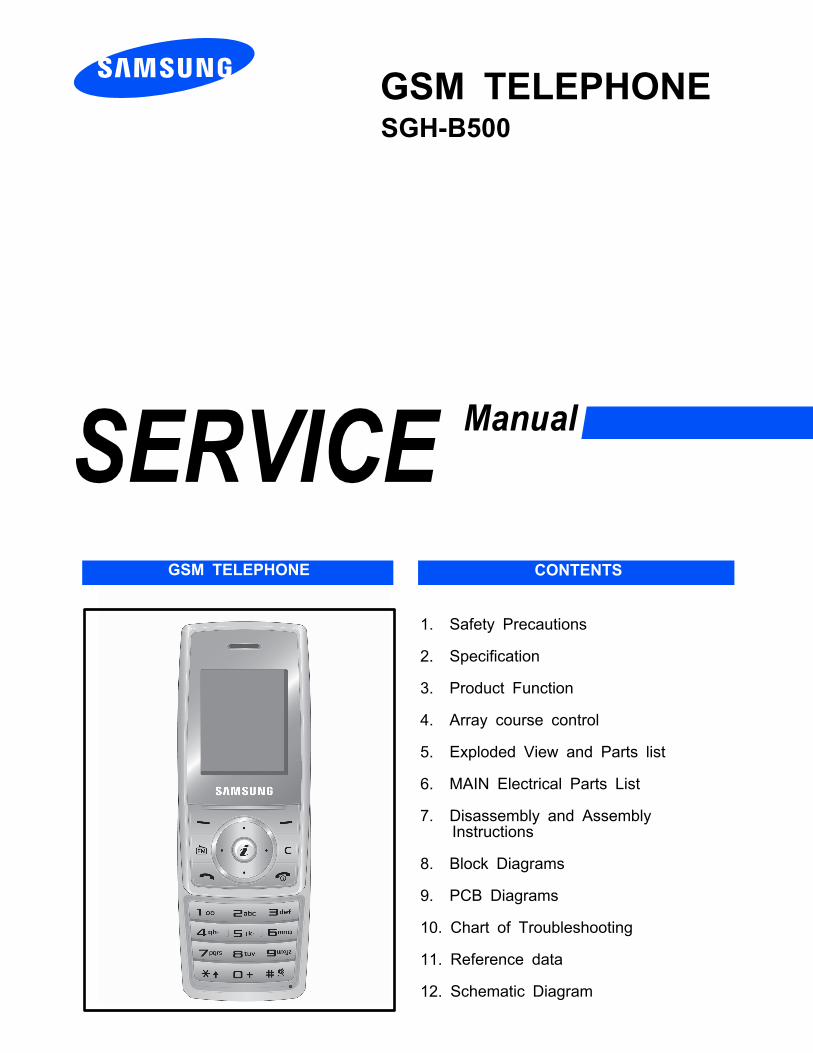
GSM TELEPHONESGH-B500
GSM TELEPHONE CONTENTS
1. Safety Precautions
2. Specification
3. Product Function
4. Array course control
5. Exploded View and Parts list
6. MAIN Electrical Parts List
7. Disassembly and AssemblyInstructions
8. Block Diagrams
9. PCB Diagrams
10. Chart of Troubleshooting
11. Reference data
12. Schematic Diagram
This Service Manual is a property of Samsung Electronics Co.,Ltd.Any unauthorized use of Manual can be punished under applicableInternational and/or domestic law.
Samsung Electronics Co.,Ltd.
2007. 11. Rev.1.0
ⓒ
Country Web SiteNorth America service.samsungportal.comLatin America latin.samsungportal.comCIS cis.samsungportal.comEurope europe.samsungportal.comChina china.samsungportal.comAsia asia.samsungportal.comMideast & Africa mea.samsungportal.com
GSPN (Global Service Partner Network)
SAMSUNG Proprietary-Contents may change without notice
1. Safety Precautions
1-1
This Document can not be used without Samsung's authorization
1-1. Repair Precaution
● Repair in Shield Box, during detailed tuning.Take specially care of tuning or test,because specipicty of cellular phone is sensitive for surrounding interference(RF noise).
● Be careful to use a kind of magnetic object or tool,because performance of parts is damaged by the influence of manetic force.
● Surely use a standard screwdriver when you disassemble this product,otherwise screw will be worn away.
● Use a thicken twisted wire when you measure level.A thicken twisted wire has low resistance, therefore error of measurement is few.
● Repair after separate Test Pack and Set because for short danger (for example anovercurrent and furious flames of parts etc) when you repair board in condition ofconnecting Test Pack and tuning on.
● Take specially care of soldering, because Land of PCB is small and weak in heat.
● Surely tune on/off while using AC power plug, because a repair of battery charger isdangerous when tuning ON/OFF PBA and Connector after disassembing charger.
● Don't use as you pleases after change other material than replacement registered on SECSystem.Otherwise engineer in charge isn't charged with problem that you don't keep this rules.

SAMSUNG Proprietary-Contents may change without notice
Safety Precautions
1-2
This Document can not be used without Samsung's authorization
1-2. ESD(Electrostatically Sensitive Devices) Precaution
Several semiconductor may be damaged easilly by static electricity. Such parts are called byESD(Electrostatically Sensitive Devices), for example IC,BGA chip etc. Read Precaution below.You can prevent from ESD damage by static electricity.
● Remove static electricity remained your body before you touch semiconductor or parts withsemiconductor. There are ways that you touch an earthed place or wear static electricityprevention string on wrist.
● Use earthed soldering steel when you connect or disconnect ESD.
● Use soldering removing tool to break static electricity. , otherwise ESD will be damaged bystatic electricity.
● Don't unpack until you set up ESD on product. Because most of ESD are packed by boxand aluminum plate to have conductive power,they are prevented from static electricity.
● You must maintain electric contact between ESD and place due to be set up until ESD isconnected completely to the proper place or a circuit board.
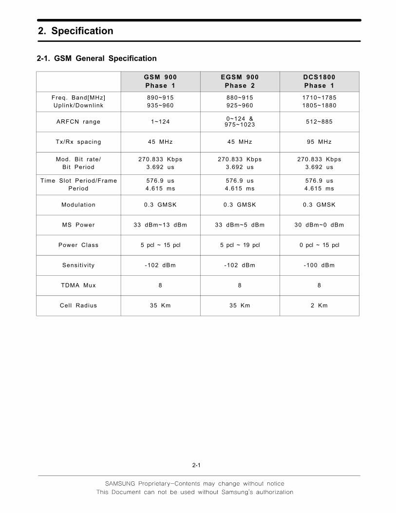
2. Specification
2-1
2-1. GSM General Specification
GSM 900Phase 1
EGSM 900Phase 2
DCS1800Phase 1
Freq. Band[MHz]Upl ink/Downl ink
890~915935~960
880~915925~960
1710~17851805~1880
ARFCN range 1~124 0~124 &975~1023 512~885
Tx/Rx spacing 45 MHz 45 MHz 95 MHz
Mod. Bit rate/Bi t Per iod
270.833 Kbps3.692 us
270.833 Kbps3.692 us
270.833 Kbps3.692 us
Time Slot Per iod/FramePeriod
576.9 us4.615 ms
576.9 us4.615 ms
576.9 us4.615 ms
Modulat ion 0.3 GMSK 0.3 GMSK 0.3 GMSK
MS Power 33 dBm~13 dBm 33 dBm~5 dBm 30 dBm~0 dBm
Power Class 5 pcl ~ 15 pcl 5 pcl ~ 19 pcl 0 pcl ~ 15 pcl
Sensi t iv i ty -102 dBm -102 dBm -100 dBm
TDMA Mux 8 8 8
Cel l Radius 35 Km 35 Km 2 Km
Specification
2-2
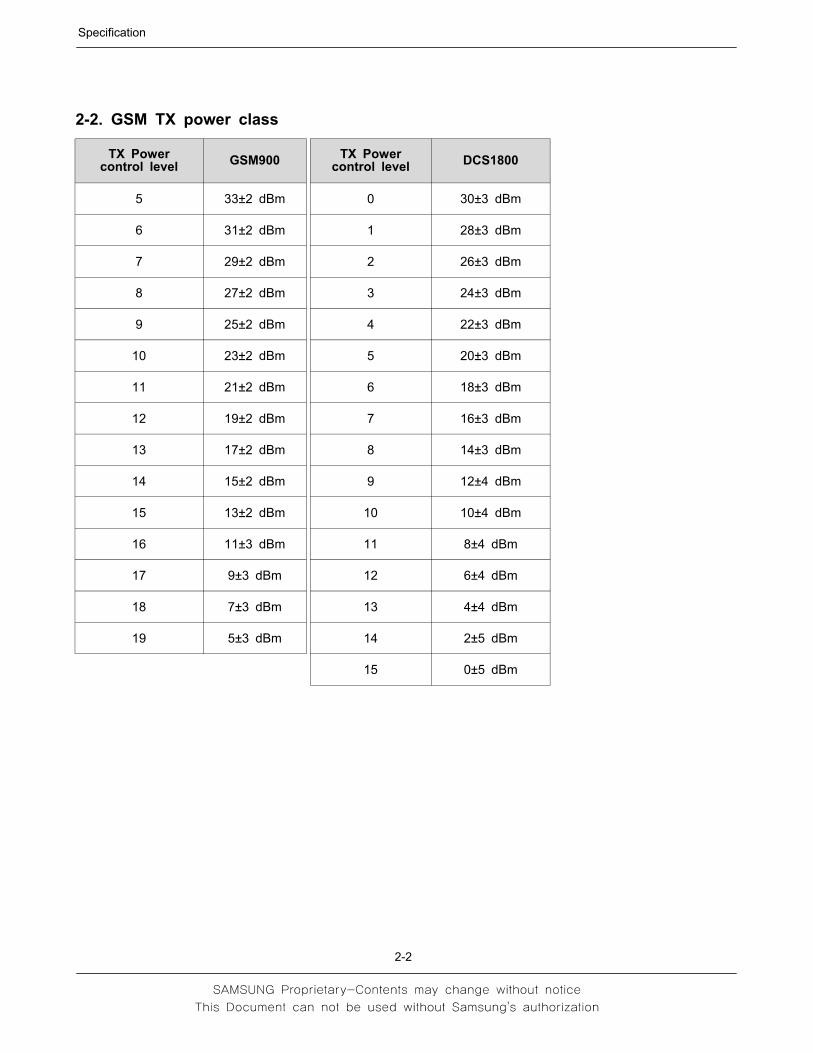
2-2. GSM TX power class
TX Powercontrol level GSM900
5 33±2 dBm
6 31±2 dBm
7 29±2 dBm
8 27±2 dBm
9 25±2 dBm
10 23±2 dBm
11 21±2 dBm
12 19±2 dBm
13 17±2 dBm
14 15±2 dBm
15 13±2 dBm
16 11±3 dBm
17 9±3 dBm
18 7±3 dBm
19 5±3 dBm
TX Powercontrol level DCS1800
0 30±3 dBm
1 28±3 dBm
2 26±3 dBm
3 24±3 dBm
4 22±3 dBm
5 20±3 dBm
6 18±3 dBm
7 16±3 dBm
8 14±3 dBm
9 12±4 dBm
10 10±4 dBm
11 8±4 dBm
12 6±4 dBm
13 4±4 dBm
14 2±5 dBm
15 0±5 dBm
SAMSUNG Proprietary-Contents may change without notice
3. Product Function
3-1
This Document can not be used without Samsung's authorization
Main Function- SDN (Service Dialling Numbers)- Music player- SOS message- FM radio
SAMSUNG Proprietary-Contents may change without notice
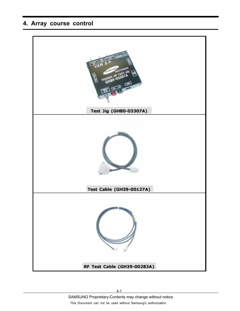
4. Array course control
4-1
This Document can not be used without Samsung's authorization
SAMSUNG Proprietary-Contents may change without notice
Array course control
4-2
This Document can not be used without Samsung's authorization
Software Downloading
4-1. Downloading Binary FilesㆍThree binary files for downloading B500
- B500XXYY.s3 : Main source code binary
4-2. Pre-requsite for DownloadingㆍDownloader Program(OptiFlash.exe)ㆍB500 Mobile PhoneㆍData CableㆍBinary files

SAMSUNG Proprietary-Contents may change without notice
Array course control
4-3
This Document can not be used without Samsung's authorization
4-3. S/W Downloader Program
1. Load the binary download program by executing the "Optiflash.exe"
2. Select the "Options" → "Settings" → "Generic" → "Specify hardwareplatform".
Choose hardware platform for the downloader file setting.Set the everything else as the default values which are shown below
SAMSUNG Proprietary-Contents may change without notice
Array course control
4-4
This Document can not be used without Samsung's authorization
3.Select the COM port when the download cable is connected
Up to twelve ports are supported. Additionally you can select the maximumtransfer speed OptiFlash will use to communicate with the phone. However,OptiFlash will use a slower speed if either the PC's or the phone's serialhardware is incapable of handling the selected speed
SAMSUNG Proprietary-Contents may change without notice
Array course control
4-5
This Document can not be used without Samsung's authorization
4. Select the "Flash&Verify" → "Browse"Set the directory path and choose the lastet s/w binary, for example"B500XXYY.s3", for the downloader binary setting.
Make sure that not to change the reserved memory regions.In case of B500 the reserved regions are :- 0x20fa0000 - 0x20fbffff0x20fd0000 - 0x20ffffff
SAMSUNG Proprietary-Contents may change without notice
Array course control
4-6
This Document can not be used without Samsung's authorization
5. Click "OK" button then press "Flash".(Before pressing 'Flash' button, push the button '*'and 'END' at the sametime. Then press 'Flash'.)
Downloader will upload the binary file as below for the downloading.
6. When downloading is finished successfully, there is a "All is well" message.
7. After finishing downloading, Certain memory resets should be done toguarantee the normal performance.
8. Confirm the downloaded version name and etc. :*#1234#
Full Reset :*2767*3855#
SAMSUNG Proprietary-Contents may change without notice
5. Exploded View and Parts List
5-1
This Document can not be used without Samsung's authorization
5-1. Cellular phone Exploded View
QMW02
QFU01
QMP01
QSP01
QRF01
QCR06QCR06
QAN01
QAR01QLC01
QPC01
QSC01
QCR06
QFL01
QMO01
QKP01
QME01
QMI01
QSH01
QSH03
QRE01
QBA01
QCR58
QBA00
QKP02
QME02
QSH02
QIF01
QRF03
QFR01
QFL02
QHI01
SAMSUNG Proprietary-Contents may change without notice
Exploded View and Parts List
5-2
This Document can not be used without Samsung's authorization
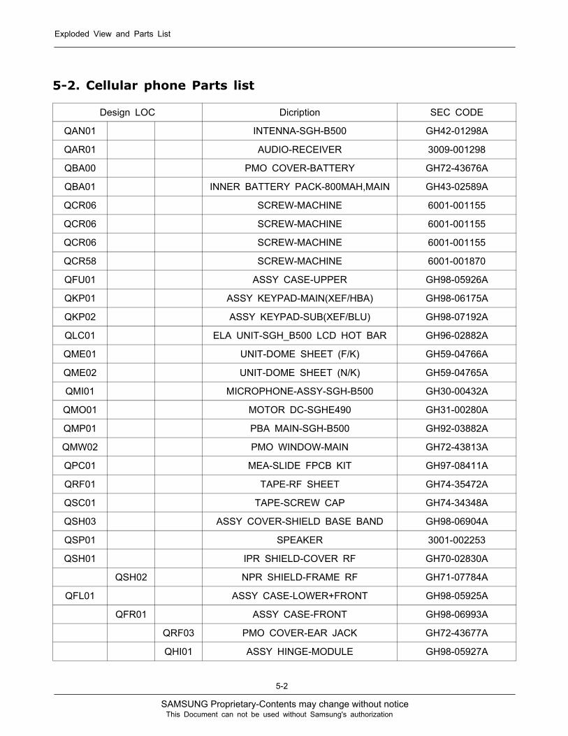
Design LOC Dicription SEC CODE
QAN01 INTENNA-SGH-B500 GH42-01298A
QAR01 AUDIO-RECEIVER 3009-001298
QBA00 PMO COVER-BATTERY GH72-43676A
QBA01 INNER BATTERY PACK-800MAH,MAIN GH43-02589A
QCR06 SCREW-MACHINE 6001-001155
QCR06 SCREW-MACHINE 6001-001155
QCR06 SCREW-MACHINE 6001-001155
QCR58 SCREW-MACHINE 6001-001870
QFU01 ASSY CASE-UPPER GH98-05926A
QKP01 ASSY KEYPAD-MAIN(XEF/HBA) GH98-06175A
QKP02 ASSY KEYPAD-SUB(XEF/BLU) GH98-07192A
QLC01 ELA UNIT-SGH_B500 LCD HOT BAR GH96-02882A
QME01 UNIT-DOME SHEET (F/K) GH59-04766A
QME02 UNIT-DOME SHEET (N/K) GH59-04765A
QMI01 MICROPHONE-ASSY-SGH-B500 GH30-00432A
QMO01 MOTOR DC-SGHE490 GH31-00280A
QMP01 PBA MAIN-SGH-B500 GH92-03882A
QMW02 PMO WINDOW-MAIN GH72-43813A
QPC01 MEA-SLIDE FPCB KIT GH97-08411A
QRF01 TAPE-RF SHEET GH74-35472A
QSC01 TAPE-SCREW CAP GH74-34348A
QSH03 ASSY COVER-SHIELD BASE BAND GH98-06904A
QSP01 SPEAKER 3001-002253
QSH01 IPR SHIELD-COVER RF GH70-02830A
QSH02 NPR SHIELD-FRAME RF GH71-07784A
QFL01 ASSY CASE-LOWER+FRONT GH98-05925A
QFR01 ASSY CASE-FRONT GH98-06993A
QRF03 PMO COVER-EAR JACK GH72-43677A
QHI01 ASSY HINGE-MODULE GH98-05927A
5-2. Cellular phone Parts list

SAMSUNG Proprietary-Contents may change without notice
Exploded View and Parts List
5-3
This Document can not be used without Samsung's authorization
QFL02 ASSY CASE-LOWER GH98-06994A
QRE01 ASSY CASE-REAR GH98-05923A
QIF01 PMO COVER-IF GH72-43675A

SAMSUNG Proprietary-Contents may change without notice
Exploded View and Parts List
5-4
This Document can not be used without Samsung's authorization
Dicription SEC CODEBAG PE 6902-000297
ADAPTOR-EU 220V TYPE(BLK) GH44-01334AEARPHONE-EARPHONE,10P,BLK(EU) GH59-04003A
LABEL(P)-UNIT SEAL GH68-00518BLABEL(P)-IMEI GH68-01335D
LABEL(R)-WATER SOAK GH68-09361ALABEL(R)-MAIN(EU) GH68-16382A
MANUAL USERS-EU ITALIAN GH68-16790ABOX(P)-UNIT MAIN(EU) GH69-06051A
TAPE INSU-FPCB CONN GH74-35379ATAPE GASK-SUB PCB GH74-35485A
TAPE GASK GH74-35486ATAPE-FPCB BACK GH74-35890A
VINYL-BOHO SLIDE GH74-36497AVINYL-BOHO LCD GH74-36898A
VINYL-BOHO REAR GH74-36899ACBF SIGNAL-SGHV200TEST GH39-00257BCBF SIGNAL-SGHV200TEST GH39-00257D
CBF SIGNAL-SPHA560 RF CABLE GH39-00397AINSTALL-TEST JIG BOX GH80-03312A
SAMSUNG Proprietary-Contents may change without notice
6. MAIN Electrical Parts List
6-1
This Document can not be used without Samsung's authorization
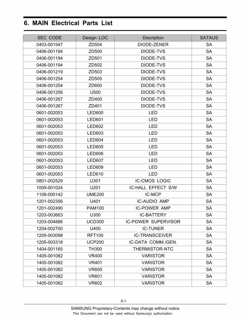
SEC CODE Design LOC Discription SATAUS0403-001547 ZD504 DIODE-ZENER SA0406-001194 ZD500 DIODE-TVS SA0406-001194 ZD501 DIODE-TVS SA0406-001194 ZD502 DIODE-TVS SA0406-001219 ZD503 DIODE-TVS SA0406-001254 ZD505 DIODE-TVS SA0406-001254 ZD600 DIODE-TVS SA0406-001256 U500 DIODE-TVS SA0406-001267 ZD400 DIODE-TVS SA0406-001267 ZD401 DIODE-TVS SA0601-002053 LED600 LED SA0601-002053 LED601 LED SA0601-002053 LED602 LED SA0601-002053 LED603 LED SA0601-002053 LED604 LED SA0601-002053 LED605 LED SA0601-002053 LED606 LED SA0601-002053 LED607 LED SA0601-002053 LED609 LED SA0601-002053 LED610 LED SA0801-002529 U301 IC-CMOS LOGIC SA1009-001024 U201 IC-HALL EFFECT S/W SA1108-000142 UME200 IC-MCP SA1201-002356 U401 IC-AUDIO AMP SA1201-002490 PAM100 IC-POWER AMP SA1203-003663 U300 IC-BATTERY SA1203-004886 UCD300 IC-POWER SUPERVISOR SA1204-002700 U400 IC-TUNER SA1205-003098 RFT100 IC-TRANSCEIVER SA1205-003318 UCP200 IC-DATA COMM./GEN. SA1404-001165 TH300 THERMISTOR-NTC SA1405-001082 VR400 VARISTOR SA1405-001082 VR401 VARISTOR SA1405-001082 VR600 VARISTOR SA1405-001082 VR601 VARISTOR SA1405-001082 VR602 VARISTOR SA

SAMSUNG Proprietary-Contents may change without notice
Main Electrical Parts List
6-2
This Document can not be used without Samsung's authorization
SEC CODE Design LOC Discription SATAUS1405-001082 VR603 VARISTOR SA1405-001082 VR610 VARISTOR SA1405-001082 VR613 VARISTOR SA1405-001082 VR614 VARISTOR SA1405-001183 VR609 VARISTOR SA1405-001183 VR611 VARISTOR SA1405-001183 VR612 VARISTOR SA2007-000139 R226 R-CHIP SA2007-000140 R518 R-CHIP SA2007-000143 R203 R-CHIP SA2007-000143 R210 R-CHIP SA2007-000144 R308 R-CHIP SA2007-000147 R206 R-CHIP SA2007-000147 R209 R-CHIP SA2007-000148 R100 R-CHIP SA2007-000148 R204 R-CHIP SA2007-000153 R402 R-CHIP SA2007-000153 R409 R-CHIP SA2007-000155 R305 R-CHIP SA2007-000157 R306 R-CHIP SA2007-000159 R307 R-CHIP SA2007-000162 R201 R-CHIP SA2007-000162 R202 R-CHIP SA2007-000162 R225 R-CHIP SA2007-000162 R300 R-CHIP SA2007-000162 R310 R-CHIP SA2007-000162 R403 R-CHIP SA2007-000162 R404 R-CHIP SA2007-000162 R500 R-CHIP SA2007-000162 R501 R-CHIP SA2007-000162 R502 R-CHIP SA2007-000162 R503 R-CHIP SA2007-000162 R504 R-CHIP SA2007-000162 R510 R-CHIP SA2007-000162 R524 R-CHIP SA2007-000171 R102 R-CHIP SA
SAMSUNG Proprietary-Contents may change without notice
Main Electrical Parts List
6-3
This Document can not be used without Samsung's authorization
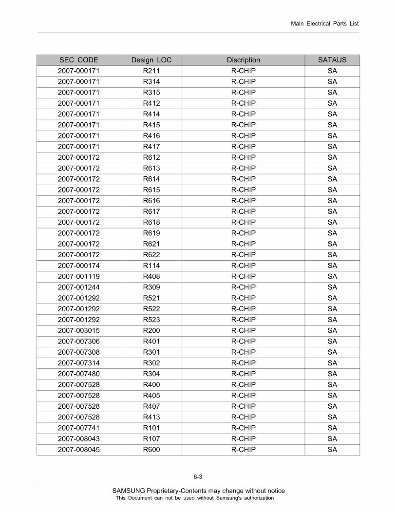
SEC CODE Design LOC Discription SATAUS2007-000171 R211 R-CHIP SA2007-000171 R314 R-CHIP SA2007-000171 R315 R-CHIP SA2007-000171 R412 R-CHIP SA2007-000171 R414 R-CHIP SA2007-000171 R415 R-CHIP SA2007-000171 R416 R-CHIP SA2007-000171 R417 R-CHIP SA2007-000172 R612 R-CHIP SA2007-000172 R613 R-CHIP SA2007-000172 R614 R-CHIP SA2007-000172 R615 R-CHIP SA2007-000172 R616 R-CHIP SA2007-000172 R617 R-CHIP SA2007-000172 R618 R-CHIP SA2007-000172 R619 R-CHIP SA2007-000172 R621 R-CHIP SA2007-000172 R622 R-CHIP SA2007-000174 R114 R-CHIP SA2007-001119 R408 R-CHIP SA2007-001244 R309 R-CHIP SA2007-001292 R521 R-CHIP SA2007-001292 R522 R-CHIP SA2007-001292 R523 R-CHIP SA2007-003015 R200 R-CHIP SA2007-007306 R401 R-CHIP SA2007-007308 R301 R-CHIP SA2007-007314 R302 R-CHIP SA2007-007480 R304 R-CHIP SA2007-007528 R400 R-CHIP SA2007-007528 R405 R-CHIP SA2007-007528 R407 R-CHIP SA2007-007528 R413 R-CHIP SA2007-007741 R101 R-CHIP SA2007-008043 R107 R-CHIP SA2007-008045 R600 R-CHIP SA
SAMSUNG Proprietary-Contents may change without notice
Main Electrical Parts List
6-4
This Document can not be used without Samsung's authorization
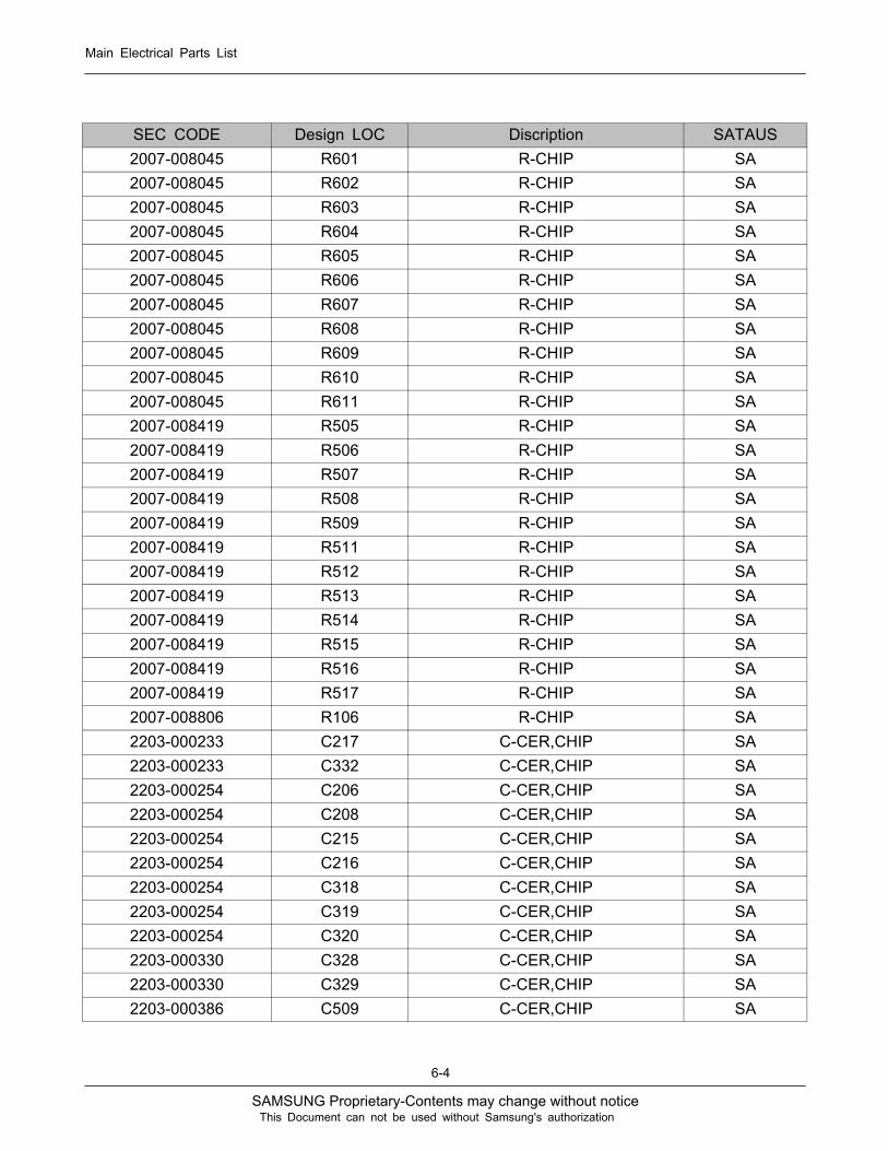
SEC CODE Design LOC Discription SATAUS2007-008045 R601 R-CHIP SA2007-008045 R602 R-CHIP SA2007-008045 R603 R-CHIP SA2007-008045 R604 R-CHIP SA2007-008045 R605 R-CHIP SA2007-008045 R606 R-CHIP SA2007-008045 R607 R-CHIP SA2007-008045 R608 R-CHIP SA2007-008045 R609 R-CHIP SA2007-008045 R610 R-CHIP SA2007-008045 R611 R-CHIP SA2007-008419 R505 R-CHIP SA2007-008419 R506 R-CHIP SA2007-008419 R507 R-CHIP SA2007-008419 R508 R-CHIP SA2007-008419 R509 R-CHIP SA2007-008419 R511 R-CHIP SA2007-008419 R512 R-CHIP SA2007-008419 R513 R-CHIP SA2007-008419 R514 R-CHIP SA2007-008419 R515 R-CHIP SA2007-008419 R516 R-CHIP SA2007-008419 R517 R-CHIP SA2007-008806 R106 R-CHIP SA2203-000233 C217 C-CER,CHIP SA2203-000233 C332 C-CER,CHIP SA2203-000254 C206 C-CER,CHIP SA2203-000254 C208 C-CER,CHIP SA2203-000254 C215 C-CER,CHIP SA2203-000254 C216 C-CER,CHIP SA2203-000254 C318 C-CER,CHIP SA2203-000254 C319 C-CER,CHIP SA2203-000254 C320 C-CER,CHIP SA2203-000330 C328 C-CER,CHIP SA2203-000330 C329 C-CER,CHIP SA2203-000386 C509 C-CER,CHIP SA

SAMSUNG Proprietary-Contents may change without notice
Main Electrical Parts List
6-5
This Document can not be used without Samsung's authorization
SEC CODE Design LOC Discription SATAUS2203-000627 C125 C-CER,CHIP SNA2203-000627 C500 C-CER,CHIP SNA2203-000627 C501 C-CER,CHIP SNA2203-000812 C111 C-CER,CHIP SA2203-000812 C113 C-CER,CHIP SA2203-000812 C114 C-CER,CHIP SA2203-000812 C336 C-CER,CHIP SA2203-000812 C337 C-CER,CHIP SA2203-000812 C339 C-CER,CHIP SA2203-000812 C340 C-CER,CHIP SA2203-000812 C413 C-CER,CHIP SA2203-000812 C414 C-CER,CHIP SA2203-000812 C415 C-CER,CHIP SA2203-000812 C416 C-CER,CHIP SA2203-000812 C633 C-CER,CHIP SA2203-000940 C629 C-CER,CHIP SA2203-000995 C202 C-CER,CHIP SA2203-000995 C502 C-CER,CHIP SA2203-000995 C503 C-CER,CHIP SA2203-000995 C630 C-CER,CHIP SA2203-001124 C317 C-CER,CHIP DNA2203-001201 C101 C-CER,CHIP SA2203-002709 C204 C-CER,CHIP SA2203-002709 C301 C-CER,CHIP SA2203-002709 C302 C-CER,CHIP SA2203-002709 C303 C-CER,CHIP SA2203-002709 C304 C-CER,CHIP SA2203-002709 C305 C-CER,CHIP SA2203-002709 C307 C-CER,CHIP SA2203-002709 C330 C-CER,CHIP SA2203-005234 C103 C-CER,CHIP SA2203-005482 C104 C-CER,CHIP SA2203-005482 C200 C-CER,CHIP SA2203-005482 C201 C-CER,CHIP SA2203-005482 C205 C-CER,CHIP SA2203-005482 C207 C-CER,CHIP SA
SAMSUNG Proprietary-Contents may change without notice
Main Electrical Parts List
6-6
This Document can not be used without Samsung's authorization
SEC CODE Design LOC Discription SATAUS2203-005482 C209 C-CER,CHIP SA2203-005482 C210 C-CER,CHIP SA2203-005482 C211 C-CER,CHIP SA2203-005482 C212 C-CER,CHIP SA2203-005483 C400 C-CER,CHIP SA2203-005483 C402 C-CER,CHIP SA2203-005483 C405 C-CER,CHIP SA2203-005483 C411 C-CER,CHIP SA2203-005682 C126 C-CER,CHIP SA2203-005682 C603 C-CER,CHIP SA2203-005682 C604 C-CER,CHIP SA2203-005682 C605 C-CER,CHIP SA2203-005682 C606 C-CER,CHIP SA2203-005682 C607 C-CER,CHIP SA2203-005682 C608 C-CER,CHIP SA2203-005682 C609 C-CER,CHIP SA2203-005682 C610 C-CER,CHIP SA2203-005682 C611 C-CER,CHIP SA2203-005682 C612 C-CER,CHIP SA2203-005682 C613 C-CER,CHIP SA2203-005682 C614 C-CER,CHIP SA2203-005682 C615 C-CER,CHIP SA2203-005682 C616 C-CER,CHIP SA2203-005682 C618 C-CER,CHIP SA2203-005682 C619 C-CER,CHIP SA2203-005682 C620 C-CER,CHIP SA2203-005682 C621 C-CER,CHIP SA2203-005682 C622 C-CER,CHIP SA2203-005682 C623 C-CER,CHIP SA2203-005682 C624 C-CER,CHIP SA2203-005682 C625 C-CER,CHIP SA2203-005682 C626 C-CER,CHIP SA2203-005682 C627 C-CER,CHIP SA2203-005682 C628 C-CER,CHIP SA2203-005683 C105 C-CER,CHIP SA2203-005683 C107 C-CER,CHIP SA
SAMSUNG Proprietary-Contents may change without notice
Main Electrical Parts List
6-7
This Document can not be used without Samsung's authorization
SEC CODE Design LOC Discription SATAUS2203-005719 C108 C-CER,CHIP SA2203-005719 C110 C-CER,CHIP SA2203-005719 C115 C-CER,CHIP SA2203-005719 C117 C-CER,CHIP SA2203-005719 C119 C-CER,CHIP SA2203-005731 C106 C-CER,CHIP SA2203-005731 C109 C-CER,CHIP SA2203-005736 C112 C-CER,CHIP SA2203-006048 C213 C-CER,CHIP SA2203-006048 C214 C-CER,CHIP SA2203-006048 C334 C-CER,CHIP SA2203-006048 C408 C-CER,CHIP SA2203-006048 C508 C-CER,CHIP SA2203-006048 C601 C-CER,CHIP SA2203-006048 C602 C-CER,CHIP SA2203-006048 C617 C-CER,CHIP SA2203-006048 C631 C-CER,CHIP SA2203-006137 C409 C-CER,CHIP SA2203-006137 C506 C-CER,CHIP SA2203-006194 C118 C-CER,CHIP SA2203-006194 C122 C-CER,CHIP SA2203-006260 C128 C-CER,CHIP SA2203-006348 C313 C-CER,CHIP SA2203-006361 C300 C-CER,CHIP SA2203-006361 C311 C-CER,CHIP SA2203-006399 C335 C-CER,CHIP SA2203-006423 C116 C-CER,CHIP SA2203-006423 C130 C-CER,CHIP SA2203-006423 C131 C-CER,CHIP SA2203-006423 C422 C-CER,CHIP SA2203-006462 C129 C-CER,CHIP SA2203-006474 C333 C-CER,CHIP SA2203-006556 C127 C-CER,CHIP SA2203-006562 C312 C-CER,CHIP SA2203-006562 C314 C-CER,CHIP SA2203-006562 C315 C-CER,CHIP SA

SAMSUNG Proprietary-Contents may change without notice
Main Electrical Parts List
6-8
This Document can not be used without Samsung's authorization
SEC CODE Design LOC Discription SATAUS2203-006562 C321 C-CER,CHIP SA2203-006562 C322 C-CER,CHIP SA2203-006562 C323 C-CER,CHIP SA2203-006562 C324 C-CER,CHIP SA2203-006562 C325 C-CER,CHIP SA2203-006562 C326 C-CER,CHIP SA2203-006562 C401 C-CER,CHIP SA2203-006562 C403 C-CER,CHIP SA2203-006562 C406 C-CER,CHIP SA2203-006562 C407 C-CER,CHIP SA2203-006562 C600 C-CER,CHIP SA2203-006626 C121 C-CER,CHIP SA2203-006648 C417 C-CER,CHIP SA2203-006648 C418 C-CER,CHIP SA2203-006838 C203 C-CER,CHIP SA2203-006838 C316 C-CER,CHIP SA2203-006838 C327 C-CER,CHIP SA2203-006838 C421 C-CER,CHIP SA2404-001381 TA402 C-TA,CHIP SA2404-001406 TA502 C-TA,CHIP SA2404-001414 TA400 C-TA,CHIP SA2404-001414 TA401 C-TA,CHIP SA2404-001415 TA100 C-TA,CHIP SA2703-001180 L103 INDUCTOR-SMD SA2703-001236 L108 INDUCTOR-SMD SA2703-001722 L106 INDUCTOR-SMD SA2703-001737 L101 INDUCTOR-SMD SA2703-001737 L102 INDUCTOR-SMD SA2703-001851 L504 INDUCTOR-SMD SA2703-002484 L105 INDUCTOR-SMD SA2703-002558 L402 INDUCTOR-SMD SA2703-002558 L403 INDUCTOR-SMD SA2703-003184 L300 INDUCTOR-SMD SA2801-004466 OSC300 CRYSTAL-SMD SA2801-004587 OSC100 CRYSTAL-SMD SA2904-001592 F101 FILTER-SAW SA
SAMSUNG Proprietary-Contents may change without notice
Main Electrical Parts List
6-9
This Document can not be used without Samsung's authorization
SEC CODE Design LOC Discription SATAUS2904-001599 F102 FILTER-SAW SA3301-001534 L400 BEAD-SMD SA3301-001534 L401 BEAD-SMD SA3301-001729 L200 BEAD-SMD SA3301-001812 L502 BEAD-SMD SA3301-001812 L503 BEAD-SMD SA3301-001885 L500 BEAD-SMD SA3301-001885 L501 BEAD-SMD SA3301-001885 L505 BEAD-SMD SA3301-001912 L404 BEAD-SMD SA3705-001358 RFS100 CONNECTOR-COAXIAL SA3709-001451 SIM600 CONNECTOR-CARD EDGE SA3710-001611 IFC500 SOCKET-INTERFACE SA3711-006119 HDC600 HEADER-BOARD TO BOARD SA3711-006228 BTC500 HEADER-BATTERY SA3722-002181 EAR500 JACK-EAR PHONE SA4302-001130 BAT300 BATTERY-LI(2ND) SAGH70-02367A FPC100 ICT-ON-BOARD CLIP SAGH70-02367A FPC101 ICT-ON-BOARD CLIP SAGH70-02367A FPC102 ICT-ON-BOARD CLIP SAGH70-02367A FPC103 ICT-ON-BOARD CLIP SAGH70-02367A FPC104 ICT-ON-BOARD CLIP SA
Please consult the GSPN website (Samsung Portal) for the most recent version of the product'spart list.
SAMSUNG Proprietary-Contents may change without notice
7. Disassembly and Assembly Instructions
7-1
This Document can not be used without Samsung's authorization
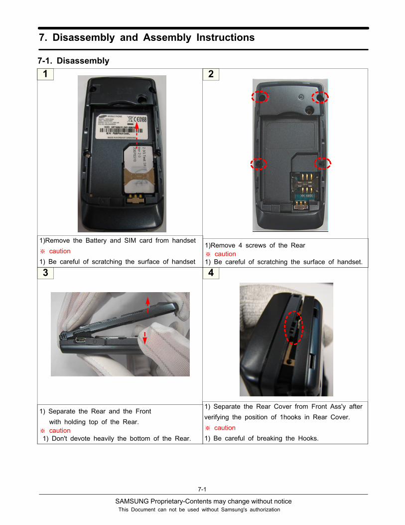
7-1. Disassembly1
43
2
1) Separate the Rear Cover from Front Ass'y afterverifying the position of 1hooks in Rear Cover.
※ caution1) Be careful of breaking the Hooks.
1)Remove the Battery and SIM card from handset
※ caution1) Be careful of scratching the surface of handset
1)Remove 4 screws of the Rear※ caution1) Be careful of scratching the surface of handset.
1) Separate the Rear and the Frontwith holding top of the Rear.
※ caution1) Don't devote heavily the bottom of the Rear.
SAMSUNG Proprietary-Contents may change without notice
Exploded View and Parts List
7-2
This Document can not be used without Samsung's authorization
5
87
6
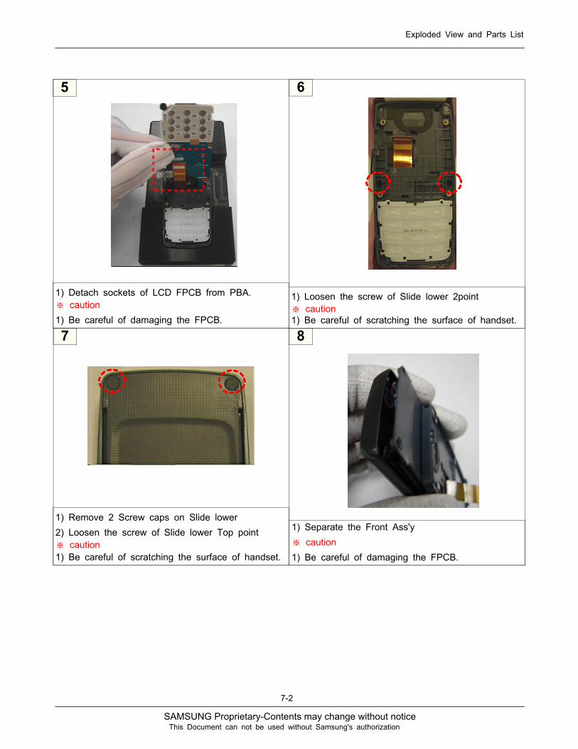
1) Loosen the screw of Slide lower 2point※ caution1) Be careful of scratching the surface of handset.
1) Detach sockets of LCD FPCB from PBA.※ caution1) Be careful of damaging the FPCB.
1) Remove 2 Screw caps on Slide lower2) Loosen the screw of Slide lower Top point※ caution1) Be careful of scratching the surface of handset.
1) Separate the Front Ass'y
※ caution1) Be careful of damaging the FPCB.

SAMSUNG Proprietary-Contents may change without notice
Exploded View and Parts List
7-3
This Document can not be used without Samsung's authorization
9
11
10
1) Separate the LCD module
※ caution1) Be careful of damaging LCD and FPCB
1) Separate the LCD module
※ caution1) Be careful of scratching the surface of handset.
1) Remove the KEY FPCB
※ caution1) Be careful of damaging the FPCB.
SAMSUNG Proprietary-Contents may change without notice
Exploded View and Parts List
7-4
This Document can not be used without Samsung's authorization
7-2. Assembly1
43
2
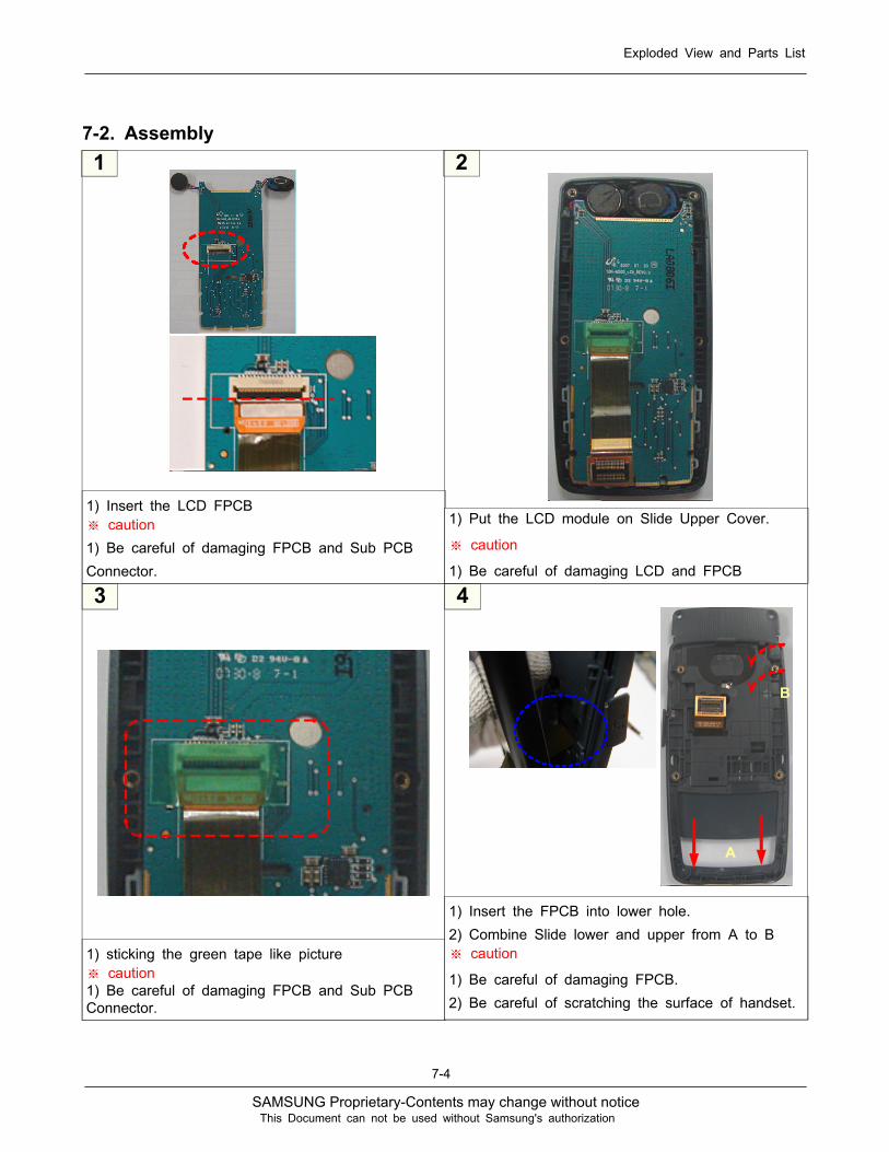
1) sticking the green tape like picture※ caution1) Be careful of damaging FPCB and Sub PCBConnector.
1) Insert the LCD FPCB※ caution1) Be careful of damaging FPCB and Sub PCBConnector.
1) Put the LCD module on Slide Upper Cover.
※ caution
1) Be careful of damaging LCD and FPCB
1) Insert the FPCB into lower hole.2) Combine Slide lower and upper from A to B※ caution
1) Be careful of damaging FPCB.2) Be careful of scratching the surface of handset.
A
B
SAMSUNG Proprietary-Contents may change without notice
Exploded View and Parts List
7-5
This Document can not be used without Samsung's authorization
5
87
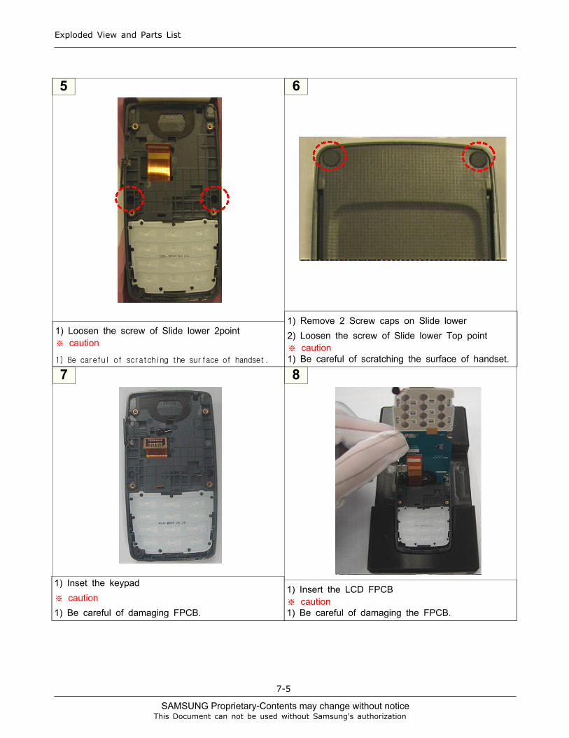
1) Insert the LCD FPCB※ caution1) Be careful of damaging the FPCB.
1) Loosen the screw of Slide lower 2point※ caution
1) Be careful of scratching the surface of handset.
1) Remove 2 Screw caps on Slide lower2) Loosen the screw of Slide lower Top point※ caution1) Be careful of scratching the surface of handset.
1) Inset the keypad
※ caution1) Be careful of damaging FPCB.
6
SAMSUNG Proprietary-Contents may change without notice
Exploded View and Parts List
7-6
This Document can not be used without Samsung's authorization
9
11
10
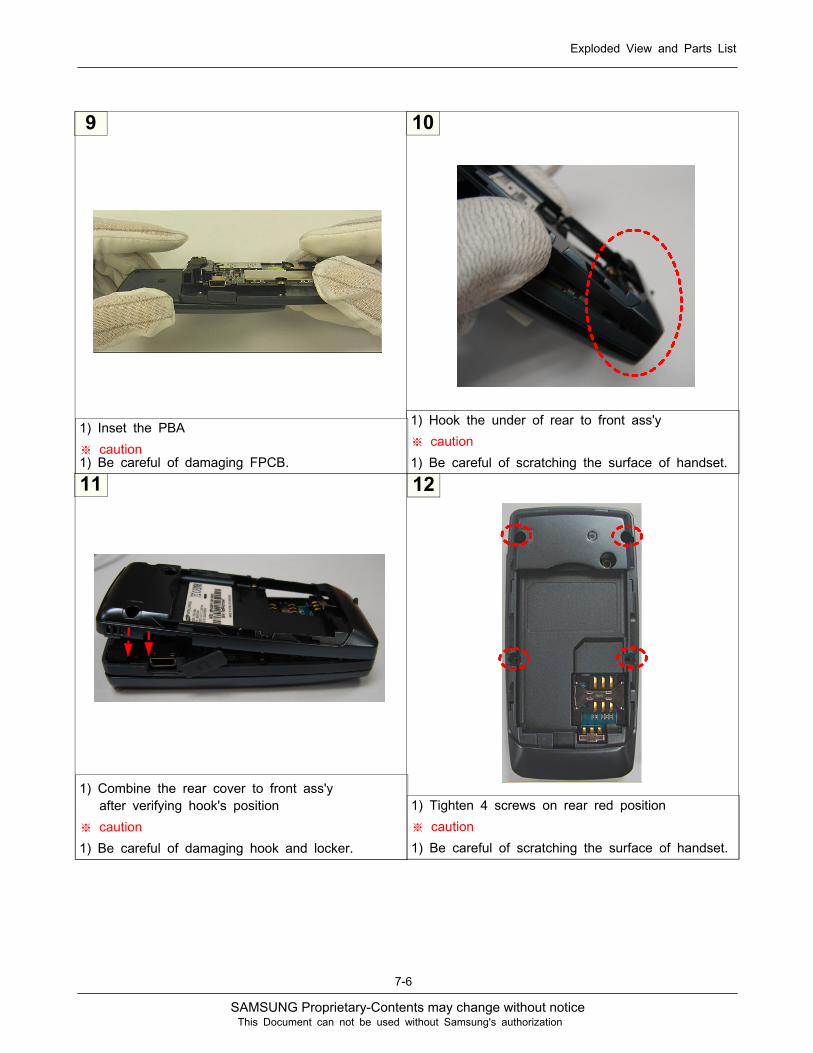
1) Hook the under of rear to front ass'y
※ caution1) Be careful of scratching the surface of handset.
1) Inset the PBA
※ caution1) Be careful of damaging FPCB.
1) Combine the rear cover to front ass'yafter verifying hook's position
※ caution1) Be careful of damaging hook and locker.
1) Tighten 4 screws on rear red position
※ caution1) Be careful of scratching the surface of handset.
12
SAMSUNG Proprietary-Contents may change without notice
8. Block Diagrams
8-1
This Document can not be used without Samsung's authorization
`

SAMSUNG Proprietary-Contents may change without notice
9. PCB Diagrams
9-1
This Document can not be used without Samsung's authorization
A(0)ADD_VALID
ANT100ANT101
BAT30 0
BTC500
C101C102
C103
C104
C105
C106
C107
C108
C109
C110
C111
C112
C113
C114
C115
C116
C117
C118
C119
C121
C122
C125
C126
C127
C128
C129
C130
C131
C200C
201
C202
C203C204
C205C206
C207
C208
C209C210
C211
C212
C215
C216
C217
C300
C301
C302
C303
C304
C305
C30 6
C307
C311
C312
C313
C314
C315
C316
C317
C318
C319C320
C321
C322C323
C324
C325
C326
C327
C328
C329
C330
C332
C33 3
C334
C335
C336C337
C338
C339C340
C400C401C402
C403
C404
C405
C406
C407
C408
C409
C410C
411
C412
C413
C414
C415C416
C417C418C421
C422
C500C501
C502
C503
C508
C509
C629
C630
C631
C632
C633
CP_OEN_SCP_WEN_S D(0)
EAR500
F101
F102
101
CPF
001
CPF
FPC102
FPC103
FPC10 4
G1 G2
G3G4
GND
GND_SW
IFC500
JCON200
JIG_ON
L101L10 2
L103
L104
L105L106
L108
L109
L112
L300L400
L401 L402L403
L500
L501
L502L503
L504
L505
MIC400
OSC100
OSC300
PAM100
R100
R101
R102
R106
R107
R114
R200
R202
R203
R204
R205
R206
R207
R208
R209
R210R
211
R224
R226
R300
R301
R302
R304R305
R306
R307
R308
R309R310
R314
R315
R400R401R402
R403
R404
R405
R406R407R408
R409
R412R
413 R414R415
R416R417
R500
R501
R502
R503
R504R
50 5R
50 6R
507R
50 8R
509R
511R
51 2R
513R
514R
515R
516R
517
R521R522
R523
R524
RAM_CS_SRDY_WAIT
RFS100
RFT100
ROM_CS_S
SC100
SDS_RXDSDS_TXD
SIM600
SM_CLK
SPK400
TA100
TA400
TA401
TA402
TA502
TH300
U300U301
U400
U401
U500
UC
D30 0
UC
P20 0
UME200
VBAT
VR400
VR401
VR500
ZD400
ZD401
ZD500ZD501ZD502
ZD503
ZD504

SAMSUNG Proprietary-Contents may change without notice
PCB Diagrams
9-2
This Document can not be used without Samsung's authorization
* 0
1 2 3
4 5 6
7 8 9
C21
3C
214
C506
C60
0
C60
1C
602 C
603
C60
4C
605
C60
6
C60
7C60
8
C60
9
C61
0
C61
1
C61
2C
613
C61
4
C61
5
C61
6
C61
7
C61
8C
619
C62
0C
621
C62
2
C62
3C
624
C62
5C
626
C62
7
C62
8
CNTL_DAT_CSP GND1
HD
C60
0L200
LED600
LED601
LED602
LED
603
LED
604
LED605
LED606
LED607
LED
609
LED
610
R201
R225
R510R518
R60
0R
601
R60
2R
603
R60
4R
605
R60
6R
607
R60
8R
609
R61
0R
611
R612
R613
R614
R615
R616R617
R618
R619
R621
R622
RTCK
SHAPE
TCKTDITDOTMS
TRSTN
U20
1
VCCD_1.8V
VR
600
VR
601
VR
602
VR60
3
VR606
VR607
VR608
VR609 VR610
VR611VR612
ZD600ZD601
SAMSUNG Proprietary-Contents may change without notice
10. Flow Chart of Troubleshooting
10-1
This Document can not be used without Samsung's authorization
10-1-1. Power ON
'Power On' does not work
Voltage >=3.3V
Download again
Charge the Battery
Pin#D6 >= 2.9V Check UCD300 and C325
Pin#F3 and pin#E14=2.9V Check UCD300 and C324
Freq = 26MHzVrms >=300mVVpp≒ 900mV
Check the clock generation circuit(related to OSC100)
Check the initial operation
END
No
Yes
Yes
Yes
Yes
Yes
No
No
No
No
pin#A6 = 1.8VNo
Yes
Check the current consumption
Check the Vbat Voltage
Check the pin of UCD300
Check the clock signal at pin#21 of RFT100
Current consumption>= 100mA
Yes
SAMSUNG Proprietary-Contents may change without notice
Flow Chart of Troubleshooting
10-2
This Document can not be used without Samsung's authorization
G 2G 5
IN1
OU
T3 4
OU
T
4 5B
S
DC
S_R
X6
GS
M_R
X7
GND8
GND9
F101
16GND
GS
M_I
N17
18N
C
DC
S_IN
19V
LOG
IC2
20GNDGND
21
VR
AM
P3
TX_E
N
1VB
ATT
GND10
ANT11
GND41213
GND3
14GND2
15GND1
PAM
100
AN
T101
C10
525
V
C11
0
C11
2
L106
C10
4
R10
2
C10
3
C11
3
ANT1
00
L105
L104
V_B
ATT
C10
7
L101
F102
2G5G
1IN
OU
T3 4
OU
T
R10
0
TA10
0
C10
8
L112
C10
9
C10
625
V
C11
4
C10
2
C11
1
C10
1L1
02
L103
1
G4
RFS
100
2A
C 3
G
BA
ND
_SE
LTX
_EN
VA
PC
DPC
S_PA
M_I
N
GSM
_LN
A_I
N_N
GS
M_L
NA
_IN
_P
DC
S_L
NA_
IN_P
DC
S_L
NA_
IN_N
GS
M_P
AM
_IN
VM
OD
_EN
SAMSUNG Proprietary-Contents may change without notice
Flow Chart of Troubleshooting
10-3
This Document can not be used without Samsung's authorization
C122C121
C115
C119VCCD_2.9V
10KR101
C116
R114
L108
C128
R106
C130
R107
C118
C126
V_BATT
C129
2
GND1
GND24
HOT
1
3HOT
C117
13
VDD
15
VLDO1
16
VLDO2
9 VLDO3
OSC100
TXOP_LO10
18V
AFC
VBAT
14
VC
C_B
BI
4
VC
C_B
BQ
24V
CC
_FE
1
VC
C_R
EF
17
VCC_TXVCO
12
32
RX850
31
RX850B
30
RX900
29
RX900B
6S
CLK
SD
ATA
5
SE
N7
TXOP_HI
11
QB
22
RE
FIN
20
RE
FIN
B19 21
RE
F_O
P
28
RX1800
RX1800B
2726
RX1900
RX1900B
25
GND
33
2I
3IB
8N
C
34N
CN
C35
Q23
RFT100
*L109
VRF_2.9V
C131
C127
C125
26MHZ_DBB
AFC
GSM_PAM_IN
DPCS_PAM_IN
RTX_I_PRTX_I_N
RTX_Q_P
RTX_Q_N
DCS_LNA_IN_N
DCS_LNA_IN_P
GSM_LNA_IN_N
GSM_LNA_IN_P
SBCKSBDT
SBLE

SAMSUNG Proprietary-Contents may change without notice
Flow Chart of Troubleshooting
10-4
This Document can not be used without Samsung's authorization

SAMSUNG Proprietary-Contents may change without notice
Flow Chart of Troubleshooting
10-5
This Document can not be used without Samsung's authorization
10-1-2. Initial
Initial Failure
The pin #A6 of UCD300 =
1.8V and
the pin #D6 of UCD300 =
2.9V ?
Check the UCD300(if it has some problem, it is to be replaced.)
Yes
No
Is the pin #P5 of UCD300
"Low → High" ?
Yes
NoCheck the UCD300
(if it has some problem, it is to be replaced.)
There is 32.768kHz wave
forms at the C328 and C329
Yes
NoCheck the UCD300
The voltage is "High" at the
C316,C317,C324,C325Check the UCD300
LCD display is O.K
No
Yes
Yes
Check the LCD part
No
Sound is O.K
Yes
NoCheck the Audio part
END
Yes

SAMSUNG Proprietary-Contents may change without notice
Flow Chart of Troubleshooting
10-6
This Document can not be used without Samsung's authorization

SAMSUNG Proprietary-Contents may change without notice
Flow Chart of Troubleshooting
10-7
This Document can not be used without Samsung's authorization
C208
R226
C210
R206
C209
R200
VRF_2.9V
C217
C202C200
VCCD_2.9V
U16
TEST2U17
NC
U2
NC
U3
U5
NC
AGPIOB4U6
IRQ3U9
T4
NC
T5
IRQ0T6
NC
T7
AGPIOA7U1
TCK U12
U13CGPIOA0
ACC1TXU15
RESETN
T12
T13TEST0
ACC1RX T14
ACC0RX_IRDARX T15
CGPIOA7_ACC0DCDT16
CGPIOA3_ACC0RTST17
USIMCLKT2
NC
T3
NC
R2
NC
R4
VD
DB
1P2
R5
NC
R6
IRQ2R7
CGPIOB4_IRQ5R8
USIMIO T1
ABBCLKT11
TDO
R1
SSP2TXDR10
VD
DB
1P2
R11
PWRKEEPR12
R13CGPIOA1
CGPIOA6_ACC0RI R14
ACC0TX_IRDATXR16
VD
DU
AR
T0R
17
AGPIOA0_CPWM0_APWM0
P2
AGPIOB6P3
AGPIOA1_CPWM1_APWM1P4
P5
NC
VD
D1P
8P
6
NC
P7
SSP2FSP8
IRQ1P9
CGPIOB6_IRQ7_USIMRST
N8
VD
D1P
8P
10
TDIP11
CLKREQP12
TRSTNP13
CLK32KHZP14
CGPIOA4_ACC0DSR P15
CGPIOA5_ACC0DTRP16
AGPIOB5
N15
OCTL0N16
VD
DR
FN
17
N2FLASHRSTN
BE1NN3
D02N4
NC
N5
SSP2CLKN7
CGPIOB3_IRQ4
VS
SM
7
CGPIOB5_IRQ6M8
SSP2RXDM9
CS3NN1
TMSN10
ABBAINTN11
OCTL1N13
N14CGPIOA2_ACC0CTS
OCTL6
VS
SM
11
OCTL2M14
OCTL5M15
VS
SR
FM
16
OCTL4M17
VD
DB
1P2
M2
D10M3
D01M4
L2
A00L3
A06L4
VD
D1P
8L5
CS2NL6
VS
SL8
D03M1
TEST1 M10
K8
VS
SK
9
VS
SL1
0
VS
SL1
2
VD
DB
1P2
L13
VD
DR
FL1
4
L15RXTXEN
ABBDINTL16
NC
K13
OCTL3K14
RXTXDATK15
D11K3
D08K4
A01K5
K6
VD
D1P
8
VS
SK
7
VS
S
J14
ABBDCLK J17
D04J4
NC
J6
VS
SJ8
VS
SK
10
VS
SK
11
SCUSTBK12
ABBDDATA
H5
VD
D1P
8H
6
VS
SH
7
VS
SH
8
VS
SH
9
D09J1
VS
SJ1
0
VS
SJ1
2
TXPSTB
H10
VS
SH
11
VD
D1P
8H
12
ABBDENH13
CTRLENRFH14
AGPIOB7 H15
OEN H3
D06H4
D14CTRLCLKRF
RTCKG16
A14G2
D15G3
VD
DB
1P2
G4
BE0NG5
VD
D1P
8G
6
G8
VS
S
VS
S
F4
F7V
DD
1P8
BOOT2_A23F8
CGPIOB2F9
VS
SG
10
VS
SG
12
VD
DA
1P20
G13
CTRLDATARFG14G15
F10
F11
VD
DS
SB
UF
VD
D3P
0F1
4
VD
DB
1P2
F15
VD
DA
1P21
F16
VD
DR
FCN
TLF1
7
D13F2
CS0NF3
D12
E17
A08E2
D07E3
D05E4
AGPIOB0_SMWAITN E5
A02E7
KEY00_PWRSWBUFE8
D00F1
VD
D1P
8
D9
WENE1
KEY10_TRACEPKT6E10
E11 KEY04_TRACEPKT0
NC
E13
USBRCVE14
NC
E15
E16
NC
SYSCLK
D16
A15D2
A07D3
CS1ND4
D5A12
BOOT0_A21D6
CGPIOB0_A24D7
CS4ND8
KEY11_TRACEPKT7
C7
CLKOUT_TRACECLKC8
KEY05_TRACEPKT1D10
KEY12_TRACESYNCD11
NC
D12
AGPIOA6D13
VD
D3P
0D
14
NC
D15
NC
USBEXTINT
AGPIOA4_IRDARXC14
I2CSDAC16
VD
DM
MC
C17
A16C2
C4A18
A04C5C6
A03
A17
BOOT1_A22
A05B5
VD
DB
1P2
B6
VD
D3P
0_V
DD
OTP
B7
BOOT3_A20C1
KEY08_TRACEPKT4C10 KEY07_TRACEPKT3C11
KEY02_PIPESTAT1C12
C13
KEY01_PIPESTAT0
USBOE B13
B14
VD
DB
1P2
I2CSCLB15
AGPIOA3_IRDATXB16
NC
B17
SMADDRVALID B2
A10B3
B4
A17
A11A2
SMCLKA3
A5BOOT4_A19
CGPIOB1 A6
KEY09_TRACEPKT5A9
A13B1
KEY06_TRACEPKT2B11
B12
NC
1
NC
2
A09A1
A12KEY03_PIPESTAT2
AGIPOA2_CLKOUT1A13
USBDP_ACC0RX A15
USBDM_ACC0TXA16
AGPIOA5
VCCD_1.8V
UCP200
VCCD_1.8V
R205
C206
R207 R208 R209
C212C211
C205
VCCD_1.8V
R211
C207
C201
VCCD_1.2AV
RTCK
A(24)
DEBUG_DSR
DEBUG_RI
DLC_DETECT
FM_SDA
DEBUG_TXD
TCK
I2C_DATI2C_CLKA(8)
A(7)A(6)A(5)A(4)A(3)A(2)A(1)
A(0:18)
D(12)D(13)D(14)D(15)
D(0:15)
A(0)
A(18)A(17)A(16)A(15)A(14)A(13)A(12)A(11)A(10)A(9)
KEY_ROW(2)KEY_ROW(3)KEY_ROW(4)
KEY_ROW(0:4)
KEY_COL(0)KEY_COL(1)KEY_COL(2)KEY_COL(3)
KEY_COL(0:4)
D(0)D(1)D(2)D(3)D(4)D(5)D(6)D(7)D(8)D(9)D(10)D(11)
CP_OEN
SBLE
ABB_EN
LOWER_BYTE
SBCKSBDT
ROM1_CS
PSW1_BUF
SM_RDY_WAIT
CP_WEN
A(21)
RAM1_CS
A(20)
A(22)
SM_ADDR_VALID
VLD
O_C
OR
EA
_S
A(19)
SM_CLK
KEY_COL(4)
KEY_ROW(0)KEY_ROW(1)
RTC_CLK
TRSTN
CLK_REQ
TDI
BATT_OPEN_CHECK
SCLK_PSC
UPPER_BYTE
FLASH_RST
BAND_SEL
DEBUG_CTS
AINT
TMS
SDO_PSC
FLIP_SNS
VMOD_ENTX_EN
LCD_CS
DINT
RTX_ENRTX_DAT
ABB_DAT
SCUSTBTXPSTB
RST
SDS_TXD
CHG_OFF
BL_EN
FM_INT
SIM1_CLK
DEBUG_RTS
DEBUG_DCD
SDS_RXD
TDO
26MHZ_ABB
SIM1_DAT
VIB_RING_EN
CHG_DET
PWR_KEEP
SDI_PSC
SIM1_RST
JACK_IN
CSN_PSC
FM_SCL
DEBUG_DTR
26MHZ_DBB
DEBUG_RXD
FM_BUS_EN
EAR_SW
SAMSUNG Proprietary-Contents may change without notice
Flow Chart of Troubleshooting
10-8
This Document can not be used without Samsung's authorization
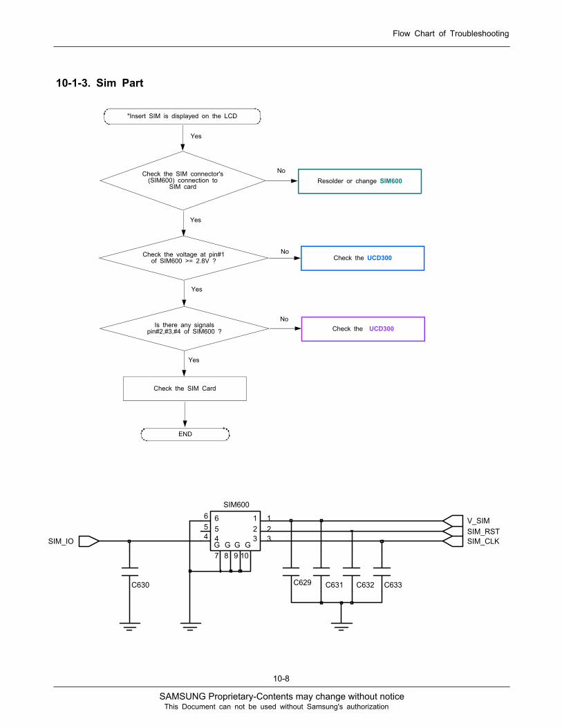
10-1-3. Sim Part
Check the voltage at pin#1of SIM600 >= 2.8V ?
"Insert SIM is displayed on the LCD
Check the SIM connector's(SIM600) connection to
SIM card
Check the UCD300
Resolder or change SIM600
END
No
Yes
Yes
Yes
Yes
No
NoIs there any signals
pin#2,#3,#4 of SIM600 ? Check the UCD300
Check the SIM Card
C633C631
7G G
8 9G G
10
1 122
3 34 455
6 6
SIM600
C630 C632C629
SIM_IO
V_SIM
SIM_CLKSIM_RST

SAMSUNG Proprietary-Contents may change without notice
Flow Chart of Troubleshooting
10-9
This Document can not be used without Samsung's authorization

SAMSUNG Proprietary-Contents may change without notice
Flow Chart of Troubleshooting
10-10
This Document can not be used without Samsung's authorization
10-1-4. Microphone Part
Is the assembled status ofmicrophone O.K?
Microphone does not work
Reassembled the microphone
Resolder or changeR402,C401,C400,C402,R400,R405,TA400,R401,C416,R415,C415,R417
END
No
Yes
Yes
Yes
Yes
No
Is microphone ok?No
Check UCD300
Check the reference voltage on mic path
VR401 ≒ 2.0V ?
Yes
①
②

SAMSUNG Proprietary-Contents may change without notice
Flow Chart of Troubleshooting
10-11
This Document can not be used without Samsung's authorization
R405
C402
R407
R401
C401
R400
C407
C411
R413
R408
R402
TA401
C400
C405
R409
TA400
EAR_MIC-MIC2_IN_N
V_MIC
MIC+
MIC-MIC1_IN_N
MIC1_IN_P
V_MIC
EAR_MIC+MIC2_IN_P

SAMSUNG Proprietary-Contents may change without notice
Flow Chart of Troubleshooting
10-12
This Document can not be used without Samsung's authorization

SAMSUNG Proprietary-Contents may change without notice
Flow Chart of Troubleshooting
10-13
This Document can not be used without Samsung's authorization
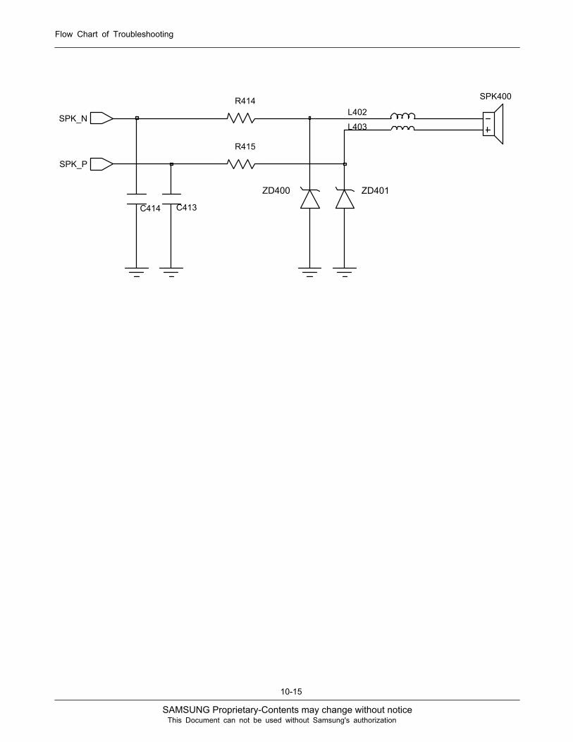
10-1-5. Receiver Part
10-1-6. Speaker Part
There is no sound from the Receiver
Is the terminal of ReceiverO.K ?
NoReplace the Receiver
Yes
No
Yes
Check UCD300
Check U101,U102 (LCD PCB Part)
Is there any signals at thepin#P11 and pin#R12 of
UCD300 ?
END
There is no sound from the Buzzer
Is the terminal of SpeakerO.K ? Replace the Speaker
Is there any signals at thepin#R13 and pin#R14 of
UCD300 ?Check U401,R414,R415
END
Yes
Yes
Yes
Yes
No
No
SAMSUNG Proprietary-Contents may change without notice
Flow Chart of Troubleshooting
10-14
This Document can not be used without Samsung's authorization
< LCD PCB Part >
SAMSUNG Proprietary-Contents may change without notice
Flow Chart of Troubleshooting
10-15
This Document can not be used without Samsung's authorization
R415
ZD401ZD400
L403
SPK400
C413C414
R414L402
SPK_P
SPK_N

SAMSUNG Proprietary-Contents may change without notice
Flow Chart of Troubleshooting
10-16
This Document can not be used without Samsung's authorization
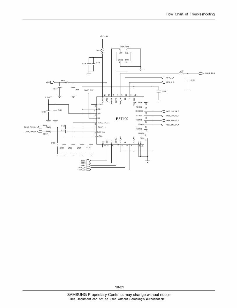
PAM100 CHECKpin11 ≥ -65dBm ?
10-2.RF
10-2-1. EGSM RX CONTINUOUS RX ON
RF INPUT : 62CH
AMP : -50dBm
NORMAL CONDITIONcatch the channel?
CHECKANT contact ?
RFT100pin 17 : 2.9V ?
PAM100 CHECKpin7 ≥ -65dBm ?
RFT100 CHECKpin29,30 ≥ -65dBm ?
PAM100,RFS100resolder or change
PAM100resolder or change
C108,C110,L106resolder or change
UCD300 pinF3,C316,C317
change or resolder
RFT100 CHECKpin 19,20
freq :26MHz ?Vp-p : 380mV?
OSC100change or resolder
RFT100resolder or change
UCD300 CHECK!!
RFT100pin 2,3,22,23 Vp-p
: 120mV ?
NO
YES
NO
NO
NO
NO
NO
NO
YES
YES
YES
YES
YES
YES
F101 CHECKpin3,4 ≥ -65dBm ?
F101resolder or change
YES
NO

SAMSUNG Proprietary-Contents may change without notice
Flow Chart of Troubleshooting
10-17
This Document can not be used without Samsung's authorization

SAMSUNG Proprietary-Contents may change without notice
Flow Chart of Troubleshooting
10-18
This Document can not be used without Samsung's authorization
PAM100 CHECKpin11 ≥ -65dBm ?
10-2-2. DCS RXCONTINUOUS RX ON
RF INPUT : 698CH
AMP : -50dBm
YES
NORMAL CONDITIONcatch the channel?
CHECKANT contact ?
RFT100pin 17 : 2.8V ?
PAM100 CHECKpin6 ≥ -65dBm ?
RFT100 CHECKpin27,28 ≥ -65dBm ?
PAM100,RFS100resolder or change
PAM100resolder or change
C105,C107,L105resolder or change
UCD300 pinF3, C317,C318change or resolder
RFT100 CHECKpin 19,20 :26MHz ?
Vp-p : 380mV?
OSC100change or resolder
RFT100resolder or change
UCD300 CHECK!!
RFT100 pin2,3,22,23 Vp-p
: 120mV ?
NO
YES
NO
NO
NO
NO
NO
YES
YES
YES
YES
YES
F102 CHECKpin3,4 ≥ -65dBm ?
F102resolder or change
YES
NO

SAMSUNG Proprietary-Contents may change without notice
Flow Chart of Troubleshooting
10-19
This Document can not be used without Samsung's authorization
10-2-3. EGSM TX
PAM100 pin11 :about 2~3 dBm?
RFS100,C101,L101,L102
check&change
PAM100pin4 : 2.8 V?
UCD300check & change
PAM100pin1 : 3.7 V?
NO NO
YES
YES
NO BATTERYcheck & change
PAM100pin 3 : 1.6V ?
YES
NO
PAM100 pin17about : -5dBm ?
YES
PAM100pin 5 : 2.9V?
YES
YES
PAM100change or resolder
NO
UCP200check
R100Check
NO
RFT100pin17 : 2.8V ?
UCD300pinF3,C316,C317
change or resolder
YES
RFT100pin19,20 : 26MHz
?Vp-p : 380mV?
RFT100pin2,3,22,23
:100mV?
YES
UCD300change or resolder
NO
NO
RFT100change or resolder
YES
NOOSC100
change or resolder
CONTINOUS TX ON CONDITIONTX POWER DAC: 600 CODE APPLIED
CH : 62RBW : 100KHzVBW : 100KHzSPAN : 10MHz
REF LEV. : 10dBmATT. : 20dB

SAMSUNG Proprietary-Contents may change without notice
Flow Chart of Troubleshooting
10-20
This Document can not be used without Samsung's authorization
10-2-4. DCS TX
CONTINUOUS TX ON CONDITIONCH : 698CH(DCS)
TX POWER CODE: 520 CODE ApliedRBW : 100KHzVBW : 100KHzSPAN : 10MHz
REF LEV. : 10dBmATT. : 20dB
PAM100 pin111 :about 2~3 dBm?
RFS100,C101,L101,L102
check&change
PAM100pin4 : 2.8 V?
UCD300check & change
PAM100pin1 : 3.7 V?
NO NO
YES
YES
NO BATTERYcheck & change
PAM100pin 3 : 1.6V ?
YES
NO
PAM100 pin19about : -5dBm ?
YES
PAM100pin 9 : 0V?
YES
YES
PAM100change or resolder
NO
UCD300check
R100Check
NO
RFT100pin17 : 2.8V ?
UCD300pinF3,C316,C317
change or resolder
YES
RFT100pin19,20 : 26MHz
?Vp-p : 380mV?
RFT100pin2,3,22,23
:100mV?
YES
UCD300change or resolder
NO
NO
YES
NOOSC100
change or resolder
RFT100change or resolder
SAMSUNG Proprietary-Contents may change without notice
Flow Chart of Troubleshooting
10-21
This Document can not be used without Samsung's authorization
C122C121
C115
C119VCCD_2.9V
R101
C116
R114
L108
C128
R106
C130
R107
C118
C126
V_BATT
C129
2
GND1
GND24
HOT
1
3HOT
C117
13
VDD
15
VLDO1
16
VLDO2
9 VLDO3
OSC100
TXOP_LO10
18VA
FC
VBAT
14
VCC
_BBI
4
VCC
_BBQ
24VC
C_F
E1
VC
C_R
EF17
VCC_TXVCO
12
32
RX850
31
RX850B
30
RX900
29
RX900B
6S
CLK
SDAT
A5
SEN
7
TXOP_HI
11
QB
22
RE
FIN
20
REF
INB
19 21R
EF_O
P
28
RX1800
RX1800B
2726
RX1900
RX1900B
25
GND
33
2I
3IB
8N
C
34N
CN
C35
Q23
RFT100
*L109
VRF_2.9V
C131
C127
C125
26MHZ_DBB
AFC
GSM_PAM_IN
DPCS_PAM_IN
RTX_I_PRTX_I_N
RTX_Q_P
RTX_Q_N
DCS_LNA_IN_N
DCS_LNA_IN_P
GSM_LNA_IN_N
GSM_LNA_IN_P
SBCKSBDT
SBLE

SAMSUNG Proprietary-Contents may change without notice
11. Reference data
11-1
This Document can not be used without Samsung's authorization
11-1. Reference Abbreviate
AAC: Advanced Audio Coding.AVC : Advanced Video Coding.BER : Bit Error RateBPSK: Binary Phase Shift KeyingCA : Conditional AccessCDM : Code Division MultiplexingC/I : Carrier to InterferenceDMB : Digital Multimedia BroadcastingEN : European StandardES : Elementary StreamETSI: European Telecommunications Standards InstituteMPEG: Moving Picture Experts GroupPN : Pseudo-random NoisePS : Pilot SymbolQPSK: Quadrature Phase Shift KeyingRS : Reed-SolomonSI : Service InformationTDM : Time Division MultiplexingTS : Transport Stream


![Home [] · 2021. 2. 24. · samsung samsung samsung samsung samsung advance advance advance advance advance advance advance advance advance advance 223sw 2233sw 2233sw 2233sw 933sn](https://static.fdocuments.in/doc/165x107/613cd1974c23507cb6359ff0/home-2021-2-24-samsung-samsung-samsung-samsung-samsung-advance-advance.jpg)