SAFC Hitech Insight Newsletter - March 2009
12
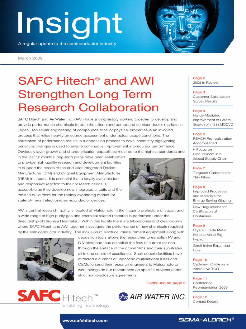
SAFC Hitech and Air Water Inc. (AWI) have a long history working together to develop and provide performance chemicals to both the silicon and compound semiconductor markets in Japan. Molecular engineering of compounds to tailor physical properties is an involved process that relies heavily on source assessment under actual usage conditions. The correlation of performance results in a deposition process to novel chemistry highlighting beneficial changes is used to ensure continuous improvement in precursor performance. Obviously layer growth and characterisation capabilities must be to the highest standards and in the last 12 months long-term plans have been established to provide high quality research and development facilities to support the needs of the end user Integrated Device Manufacturer (IDM) and Original Equipment Manufacturer (OEM) in Japan. It is essential that a locally available fast and responsive reaction to their research needs is accessible as they develop new integrated circuits and the tools to build them for the rapidly expanding market for state-of-the-art electronic semiconductor devices. AWI’s central research facility is located at Matsumoto in the Nagano prefecture of Japan and a wide range of high purity gas and chemical related research is performed under the directorship of Hirohisa Hiramatsu. Within this facility there are laboratories and clean rooms where SAFC Hitech and AWI together investigate the performance of new chemicals required by the semiconductor industry. The inclusion of electrical measurement equipment along with deposition tools allows the researcher to establish I-V and C-V plots and thus establish the flow of current (or not) through the surface of the grown films and their substrates all in one centre of excellence. Such superb facilities have attracted a number of Japanese multinational IDMs and OEMs to send their research engineers to Matsumoto to work alongside our researchers on specific projects under strict non-disclosure agreements. Continued on page 5 Insight A regular update to the semiconductor industry March 2009 SAFC Hitech ® and AWI Strengthen Long Term Research Collaboration Page 2 2008 in Review Page 3 Customer Satisfaction Survey Results Page 4 Halide Mediated Improvement of Lateral Growth of InN in MOCVD Page 6 REACH Pre-registration Accomplished A Focus on Procurement in a Global Supply Chain Page 7 Tungsten Carbonitride Thin Films Page 8 Improved Processes and Materials for Energy Saving Glazing New Regulations for Certification of Containers Page 9 Crystal Grade Metal Halides Make Big Impact Geoff Irvine Expanded Role Page 10 Cadmium Oxide as an Alternative TCO Page 11 Conference Representation 2009 Page 12 Contact Details www.safchitech.com
-
Upload
safc-global -
Category
Documents
-
view
151 -
download
2
description
2008 was an extremely successful year for SAFC Hitech with significant growthachieved despite the downturn in general economic conditions during the latter stages of the year. As well as increasing our revenues, we continued to invest inseveral areas: in expanding our manufacturing footprint in growth opportunity areas;in the development of new and innovative materials; and in the equipment with whichthese materials can be delivered to the process chamber most effectively.
Transcript of SAFC Hitech Insight Newsletter - March 2009
SAFC Hitech and Air Water Inc. (AWI) have a long history working together to develop and
provide performance chemicals to both the silicon and compound semiconductor markets in
Japan. Molecular engineering of compounds to tailor physical properties is an involved
process that relies heavily on source assessment under actual usage conditions. The
correlation of performance results in a deposition process to novel chemistry highlighting
beneficial changes is used to ensure continuous improvement in precursor performance.
Obviously layer growth and characterisation capabilities must be to the highest standards and
in the last 12 months long-term plans have been established
to provide high quality research and development facilities
to support the needs of the end user Integrated Device
Manufacturer (IDM) and Original Equipment Manufacturer
(OEM) in Japan. It is essential that a locally available fast
and responsive reaction to their research needs is
accessible as they develop new integrated circuits and the
tools to build them for the rapidly expanding market for
state-of-the-art electronic semiconductor devices.
AWI’s central research facility is located at Matsumoto in the Nagano prefecture of Japan and
a wide range of high purity gas and chemical related research is performed under the
directorship of Hirohisa Hiramatsu. Within this facility there are laboratories and clean rooms
where SAFC Hitech and AWI together investigate the performance of new chemicals required
by the semiconductor industry. The inclusion of electrical measurement equipment along with
deposition tools allows the researcher to establish I-V and
C-V plots and thus establish the flow of current (or not)
through the surface of the grown films and their substrates
all in one centre of excellence. Such superb facilities have
attracted a number of Japanese multinational IDMs and
OEMs to send their research engineers to Matsumoto to
work alongside our researchers on specific projects under
strict non-disclosure agreements.
Continued on page 5
InsightA regular update to the semiconductor industry
March 2009
SAFC Hitech® and AWIStrengthen Long TermResearch Collaboration
Page 22008 in Review
Page 3Customer SatisfactionSurvey Results
Page 4Halide MediatedImprovement of LateralGrowth of InN in MOCVD
Page 6REACH Pre-registrationAccomplished
A Focus onProcurement in aGlobal Supply Chain
Page 7Tungsten CarbonitrideThin Films
Page 8Improved Processesand Materials forEnergy Saving Glazing
New Regulations forCertification ofContainers
Page 9Crystal Grade MetalHalides Make BigImpact
Geoff Irvine ExpandedRole
Page 10Cadmium Oxide as anAlternative TCO
Page 11ConferenceRepresentation 2009
Page 12Contact Details
www.safchitech.com

2008 was an extremely successful year for SAFC Hitech with significant growth
achieved despite the downturn in general economic conditions during the latter
stages of the year. As well as increasing our revenues, we continued to invest in
several areas: in expanding our manufacturing footprint in growth opportunity areas;
in the development of new and innovative materials; and in the equipment with which
these materials can be delivered to the process chamber most effectively.
Page 2 SAFC Hitech News
2008 in Review - Barry Leese
During the year several effective campaigns have emphasised our ongoing commitment to leadership in the compound
semiconductor market, expanded our presence in the silicon semiconductor area and also entered into numerous
emerging markets for ‘performance’ or ‘specialist’ chemicals where we see substantial future business opportunities.
Investment in production facilities has seen the opening of our $9 million 5000ft² cleanroom at
Sheboygan, Wisconsin along with commissioning of additional plant capacity at
Bromborough, Haverhill and Taiwan. These expansions enable us to produce, package and
analyse products in multiple locations in higher volumes, completing the total supply chain to
ensure our customers an uninterrupted supply of the highest quality materials globally.
We hosted extremely successful media visits to both the Sheboygan and Bromborough
facilities in 2008. These visits not only gave us a chance to update our friends in the editorial
community about our ongoing investment program but also an opportunity to qualify these
investments in tangible terms by actually showing them around the expanded facilities.
Furthermore product developments were highlighted to demonstrate the advances made in
precursor technologies by our highly active Research team. In particular novel materials for
Germanium Antimony Telluride (GexSbyTez or GST) for use in high volume manufacturing phase change memory (PCM)
applications generated significant interest from several very large customers.
In October we announced the availability of our portfolio of Crystal Growth Halides representing the first launch from the
‘Performance Materials’ range of SAFC Hitech. This new element of product offerings focuses on applications outside
the “standard” Compound and Silicon areas to enhance our ability to service a wider
range of customers in the electronics and related industries. The rapidly-developing
solar market falls into this category with sol-gel, chemical bath deposition (CBD) and
other techniques as well as CVD requiring HVM of high quality chemicals. We are
already seeing major requirements for materials for CBD CIGS (copper indium
gallium selenide) and CdTe/CdSe (cadmium telluride/selenide) to complement the
existing range of CVD precursors. III-V and Si CVD sources complete the SAFC
Hitech ability to supply precursors to all the conventional competing technologies and
future investment in the organic electronics area will ensure full coverage of future
fabrication methods.
In addition to expanding our product range we have developed our equipment offering to enhance the delivery of
precursors to the deposition equipment. The introduction of the OM700, a bubbler that offers customers a cost-efficient
migration path to controlled precursor delivery for larger lot sizes, and the EpiVapor™, a cost-effective metalorganic
vapour phase distribution system that eliminates the need for localised tool bubblers and TCUs by delivering vapours
from highly volatile and sensitive pyrophoric liquids directly to MOCVD systems, has been very well received in the
market place. These enabling technologies afford a reduction in process downtime and increased safety controls.
Looking forward to 2009, we aim to maintain our highest standards of service to an expanding compound and silicon
semiconductor industry, to invest in locations and technologies that we feel will enhance our capabilities in emerging
areas such as photovoltaics, and to provide a stable supply chain to all of our customers.
Page 3
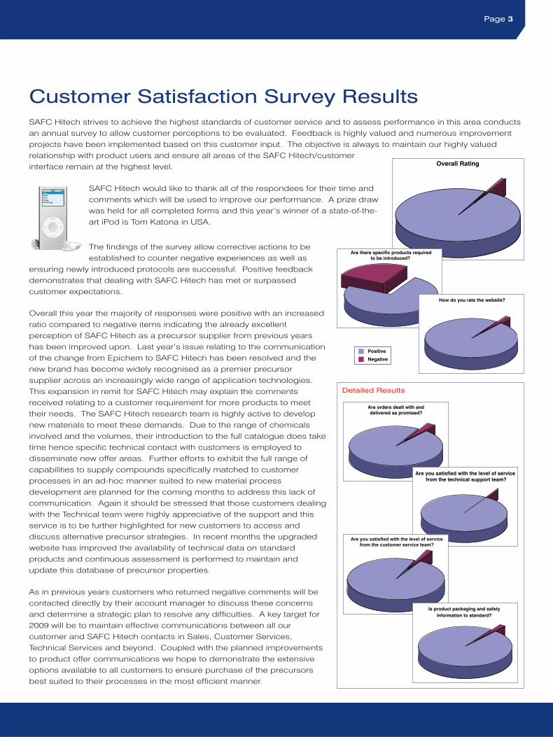
Customer Satisfaction Survey ResultsSAFC Hitech strives to achieve the highest standards of customer service and to assess performance in this area conductsan annual survey to allow customer perceptions to be evaluated. Feedback is highly valued and numerous improvementprojects have been implemented based on this customer input. The objective is always to maintain our highly valuedrelationship with product users and ensure all areas of the SAFC Hitech/customerinterface remain at the highest level.
SAFC Hitech would like to thank all of the respondees for their time andcomments which will be used to improve our performance. A prize drawwas held for all completed forms and this year’s winner of a state-of-the-art iPod is Tom Katona in USA.
Overall Rating
Positive
Negative
Detailed Results
Are orders dealt with and delivered as promised?
Are you satisfied with the level of service from the technical support team?
Are you satisfied with the level of servicefrom the customer service team?
Is product packaging and safetyinformation to standard?
The findings of the survey allow corrective actions to beestablished to counter negative experiences as well as
ensuring newly introduced protocols are successful. Positive feedbackdemonstrates that dealing with SAFC Hitech has met or surpassedcustomer expectations.
Overall this year the majority of responses were positive with an increasedratio compared to negative items indicating the already excellentperception of SAFC Hitech as a precursor supplier from previous yearshas been improved upon. Last year’s issue relating to the communicationof the change from Epichem to SAFC Hitech has been resolved and thenew brand has become widely recognised as a premier precursorsupplier across an increasingly wide range of application technologies.This expansion in remit for SAFC Hitech may explain the commentsreceived relating to a customer requirement for more products to meettheir needs. The SAFC Hitech research team is highly active to developnew materials to meet these demands. Due to the range of chemicalsinvolved and the volumes, their introduction to the full catalogue does taketime hence specific technical contact with customers is employed todisseminate new offer areas. Further efforts to exhibit the full range ofcapabilities to supply compounds specifically matched to customerprocesses in an ad-hoc manner suited to new material processdevelopment are planned for the coming months to address this lack ofcommunication. Again it should be stressed that those customers dealingwith the Technical team were highly appreciative of the support and thisservice is to be further highlighted for new customers to access anddiscuss alternative precursor strategies. In recent months the upgradedwebsite has improved the availability of technical data on standardproducts and continuous assessment is performed to maintain andupdate this database of precursor properties.
As in previous years customers who returned negative comments will becontacted directly by their account manager to discuss these concernsand determine a strategic plan to resolve any difficulties. A key target for2009 will be to maintain effective communications between all ourcustomer and SAFC Hitech contacts in Sales, Customer Services,Technical Services and beyond. Coupled with the planned improvementsto product offer communications we hope to demonstrate the extensiveoptions available to all customers to ensure purchase of the precursorsbest suited to their processes in the most efficient manner.
Are there specific products requiredto be introduced?
How do you rate the website?
In this work, we present our results regarding the progress in MOVPEgrowth of InN achieved in the INDOT project thanks to inputs from allpartners to optimise materials and processes (see inset for INDOTdetails or www.indot-project.net). First, we attempted to reproduce thesuccessful two-step growth method which is commonly used to formepitaxial GaN layers on a sapphire substrate, also with a large latticemismatch. In-depth analysis of the structure and morphology of a GaNnucleation layer in order to transpose this knowledge to theInN/GaN/sapphire system was performed. The detailed study of suchan annealed GaN buffer revealed the presence of a typical density of1011 per cm2 crystal grains, with a quality analysed by grazing X-raydiffraction that showed a full width at half maximum of 3600 arcsecondsfor the (10-10) diffraction peak. Such a test structure was producedusing the required low temperature MOVPE growth of InN on sapphire,however, it was not possible to obtain high crystal quality due to the lackof surface mobility and lateral growth, which limits the coalescence of InN during growth.
Due to the restriction of thermal energy that can be inputted to the InN system to avoid product evaporation duringgrowth, a novel chemical approach has been studied to enhance surface mobilities and allow high quality films to bedeposited. This technique involves modification of the gas phase chemistry to enhance lateral growth of InN by alteringthe surface species and increasing their ability to move on a surface even at the low temperatures dictated for InN. Indetail CBrCl3 was co-injected during growth to form volatile halides that have proven successful in enhancing the finaldeposited film quality significantly.
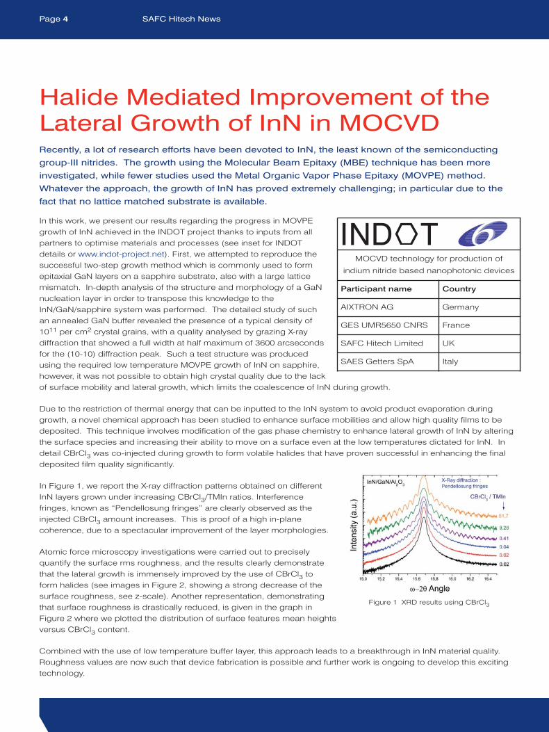
In Figure 1, we report the X-ray diffraction patterns obtained on differentInN layers grown under increasing CBrCl3/TMIn ratios. Interferencefringes, known as “Pendellosung fringes” are clearly observed as theinjected CBrCl3 amount increases. This is proof of a high in-planecoherence, due to a spectacular improvement of the layer morphologies.
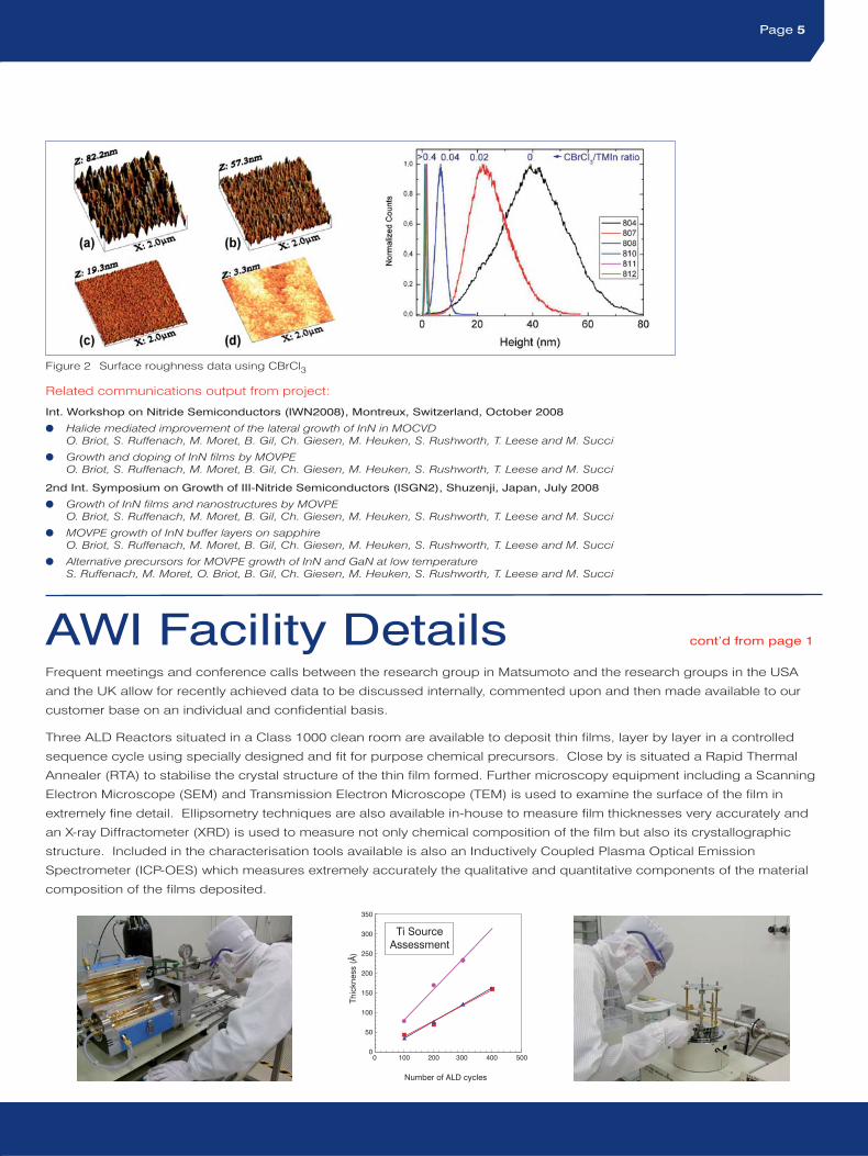
Atomic force microscopy investigations were carried out to preciselyquantify the surface rms roughness, and the results clearly demonstratethat the lateral growth is immensely improved by the use of CBrCl3 toform halides (see images in Figure 2, showing a strong decrease of thesurface roughness, see z-scale). Another representation, demonstratingthat surface roughness is drastically reduced, is given in the graph inFigure 2 where we plotted the distribution of surface features mean heightsversus CBrCl3 content.
Combined with the use of low temperature buffer layer, this approach leads to a breakthrough in InN material quality.Roughness values are now such that device fabrication is possible and further work is ongoing to develop this excitingtechnology.
Recently, a lot of research efforts have been devoted to InN, the least known of the semiconducting
group-III nitrides. The growth using the Molecular Beam Epitaxy (MBE) technique has been more
investigated, while fewer studies used the Metal Organic Vapor Phase Epitaxy (MOVPE) method.
Whatever the approach, the growth of InN has proved extremely challenging; in particular due to the
fact that no lattice matched substrate is available.
Page 4 SAFC Hitech News
Halide Mediated Improvement of theLateral Growth of InN in MOCVD
MOCVD technology for production of
indium nitride based nanophotonic devices
Participant name Country
AIXTRON AG Germany
GES UMR5650 CNRS France
SAFC Hitech Limited UK
SAES Getters SpA Italy
Figure 1 XRD results using CBrCl3
Page 5
Related communications output from project:
Int. Workshop on Nitride Semiconductors (IWN2008), Montreux, Switzerland, October 2008
● Halide mediated improvement of the lateral growth of InN in MOCVDO. Briot, S. Ruffenach, M. Moret, B. Gil, Ch. Giesen, M. Heuken, S. Rushworth, T. Leese and M. Succi
● Growth and doping of InN films by MOVPEO. Briot, S. Ruffenach, M. Moret, B. Gil, Ch. Giesen, M. Heuken, S. Rushworth, T. Leese and M. Succi
2nd Int. Symposium on Growth of III-Nitride Semiconductors (ISGN2), Shuzenji, Japan, July 2008
● Growth of InN films and nanostructures by MOVPEO. Briot, S. Ruffenach, M. Moret, B. Gil, Ch. Giesen, M. Heuken, S. Rushworth, T. Leese and M. Succi
● MOVPE growth of InN buffer layers on sapphireO. Briot, S. Ruffenach, M. Moret, B. Gil, Ch. Giesen, M. Heuken, S. Rushworth, T. Leese and M. Succi
● Alternative precursors for MOVPE growth of InN and GaN at low temperatureS. Ruffenach, M. Moret, O. Briot, B. Gil, Ch. Giesen, M. Heuken, S. Rushworth, T. Leese and M. Succi
AWI Facility Details cont’d from page 1
Frequent meetings and conference calls between the research group in Matsumoto and the research groups in the USA
and the UK allow for recently achieved data to be discussed internally, commented upon and then made available to our
customer base on an individual and confidential basis.
Three ALD Reactors situated in a Class 1000 clean room are available to deposit thin films, layer by layer in a controlled
sequence cycle using specially designed and fit for purpose chemical precursors. Close by is situated a Rapid Thermal
Annealer (RTA) to stabilise the crystal structure of the thin film formed. Further microscopy equipment including a Scanning
Electron Microscope (SEM) and Transmission Electron Microscope (TEM) is used to examine the surface of the film in
extremely fine detail. Ellipsometry techniques are also available in-house to measure film thicknesses very accurately and
an X-ray Diffractometer (XRD) is used to measure not only chemical composition of the film but also its crystallographic
structure. Included in the characterisation tools available is also an Inductively Coupled Plasma Optical Emission
Spectrometer (ICP-OES) which measures extremely accurately the qualitative and quantitative components of the material
composition of the films deposited.
Ti SourceAssessment
Number of ALD cycles
Thic
knes
s (Å
)
350
300
250
200
150
100
50
00 100 200 300 400 500
Figure 2 Surface roughness data using CBrCl3
Page 6 SAFC Hitech News
REACH Pre-registrationSuccessfully AccomplishedSigma-Aldrich is proud to announce that the first hurdle of the REACH legislation
process has been successfully completed by the pre-registering of several hundred
chemical substances.
On December 1st, 2008 at 24:00 GMT the official REACH pre-registration period ended. During the 6-month period prior
to this date importers and manufacturers of chemicals or formulations in quantities >1000kg per year in the EU had the
opportunity to pre-register their substances at the European Chemicals Agency (ECHA) to benefit from longer transition
periods for final registration. According to the latest info from the ECHA more than 47,000 companies have made more
than 2.2 million (!) pre-registrations for around 54,000 different substances - much higher than expected.
Sigma-Aldrich pre-registered over 1000 entries for 10 different legal entities in Europe. This was only the first little step of
a long ongoing and challenging process of REACH implementation, however, Sigma-Aldrich is committed to complying
with the highest safety standards to assure customer confidence and provide comprehensive information for chemical
handling and usage.
Information for customers about REACH can be found on our website:
http://www.sigmaaldrich.com/customer-service/reach.html
Sigma-Aldrich collectively purchases about one billion dollars per year of materials and services and a key factor is
ensuring the full value of the Company’s buying leverage to obtain the best quality items for the best price. Just as our
customers wish to obtain the best deal for our products we must review our own supply chain. This involves both
“direct” spend, the materials utilised in manufacturing end products sold to customers, as well as “indirect” spend - all
other goods and services needed to do business. Historically we have performed well in this area but there is always
room for improvement.
A global review is currently ongoing to ensure the most efficient
protocols are in place and the resulting benefits will be better
connectivity with suppliers and an enhanced supply chain which can
provide higher quality, time to delivery and value for money. IT solutions
will reduce paper usage in line with the corporate Green policy as well as
speeding cycle time, provide facile tracking of the status of the
requisition and purchase orders electronically including follow up with
vendors directly. These outcomes will in turn lead to reduced cost and
optimum value that can be passed on to our customers to maintain the
high quality of service they require and demand.
A Focus on Procurement in a Global Supply Chain
Sigma-Aldrich® Global Supply ChainCommon Processes - Seamless Integration - Outstanding Service
Page 7
Tungsten Carbonitride Thin FilmsA long-standing collaboration between University College London (UK) and SAFC Hitech has seen recent advances in the
field of coatings on glass. The principles behind these advances can be applied to a wide range of material systems and
have applications in a number of electronic devices to increase speed and reduce feature size.
Claire Carmalt's group at University College London, in collaboration with the SAFC Hitech
research team in Bromborough, used chemical vapour deposition (CVD) to produce thin films
of tungsten carbonitride (WNxCy) from new precursors. WNxCy can be used as an effective
barrier layer to prevent Cu migration from circuit wires into semiconducting components and
the application of CVD to apply coherent films over reduced areas significantly helps scaling
efficiencies.
The precursors investigated included a range of tungsten imido complexes to produce
compounds with ideal thermal properties for CVD. Careful tuning of the ligands surrounding
the tungsten centre was performed to optimise these thermal properties to enhance the
fabrication of tungsten carbonitride thin films in the parameter space necessary for devices. The decomposition
mechanism studies and explanation of observed thermal events for each precursor was key in determining storage stability,
transport properties and deposition temperature capabilities. A structured approach was followed to identify the highest
potential molecules in the shortest timeframe and then to demonstrate their effective use in CVD.
In practice four closely related precursors were established for growth trials and all yielded
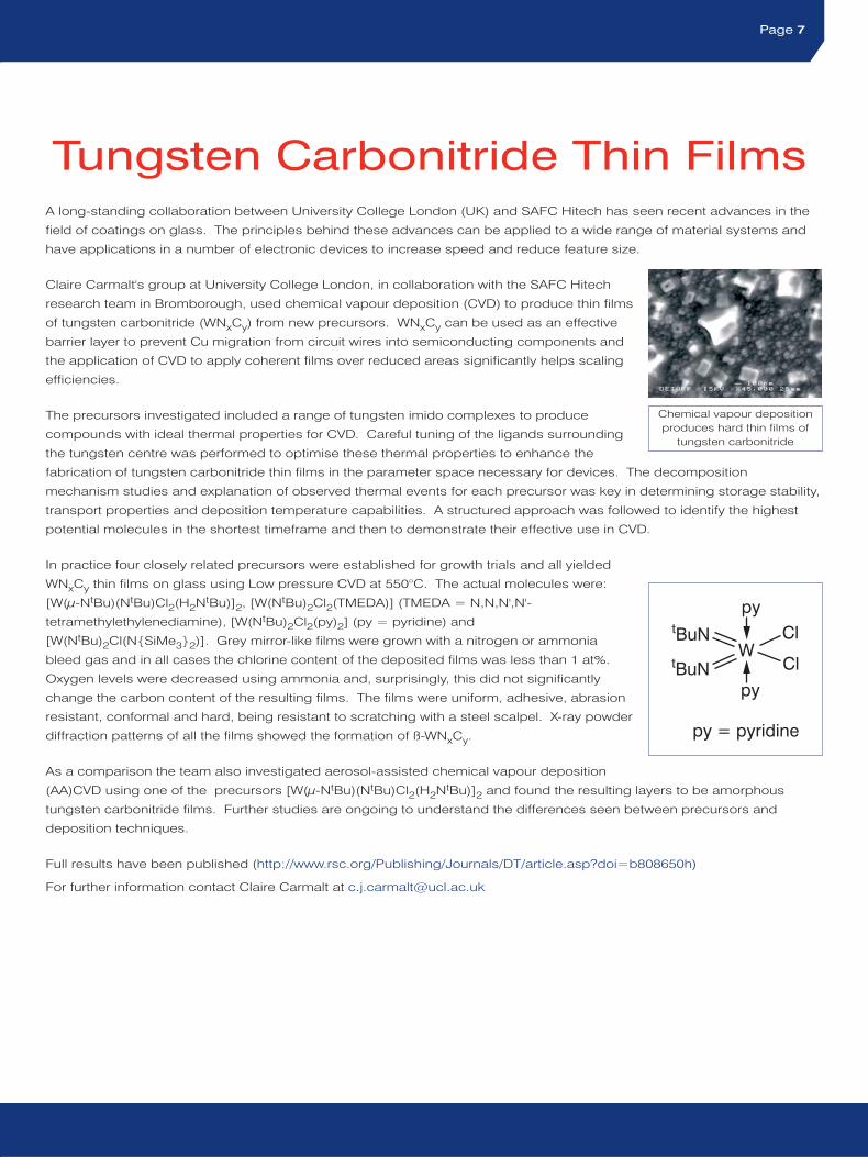
WNxCy thin films on glass using Low pressure CVD at 550°C. The actual molecules were:
[W(µ-NtBu)(NtBu)Cl2(H2NtBu)]2, [W(NtBu)2Cl2(TMEDA)] (TMEDA = N,N,N',N'-
tetramethylethylenediamine), [W(NtBu)2Cl2(py)2] (py = pyridine) and
[W(NtBu)2Cl(N{SiMe3}2)]. Grey mirror-like films were grown with a nitrogen or ammonia
bleed gas and in all cases the chlorine content of the deposited films was less than 1 at%.
Oxygen levels were decreased using ammonia and, surprisingly, this did not significantly
change the carbon content of the resulting films. The films were uniform, adhesive, abrasion
resistant, conformal and hard, being resistant to scratching with a steel scalpel. X-ray powder
diffraction patterns of all the films showed the formation of ß-WNxCy.
As a comparison the team also investigated aerosol-assisted chemical vapour deposition
(AA)CVD using one of the precursors [W(µ-NtBu)(NtBu)Cl2(H2NtBu)]2 and found the resulting layers to be amorphous
tungsten carbonitride films. Further studies are ongoing to understand the differences seen between precursors and
deposition techniques.
Full results have been published (http://www.rsc.org/Publishing/Journals/DT/article.asp?doi=b808650h)
For further information contact Claire Carmalt at [email protected]
Chemical vapour depositionproduces hard thin films of
tungsten carbonitride
pyCl
Cl
tBuN
tBuNpy
py = pyridine
W
Improved Processes and Materialsfor Energy Saving Glazing
Page 8 SAFC Hitech News
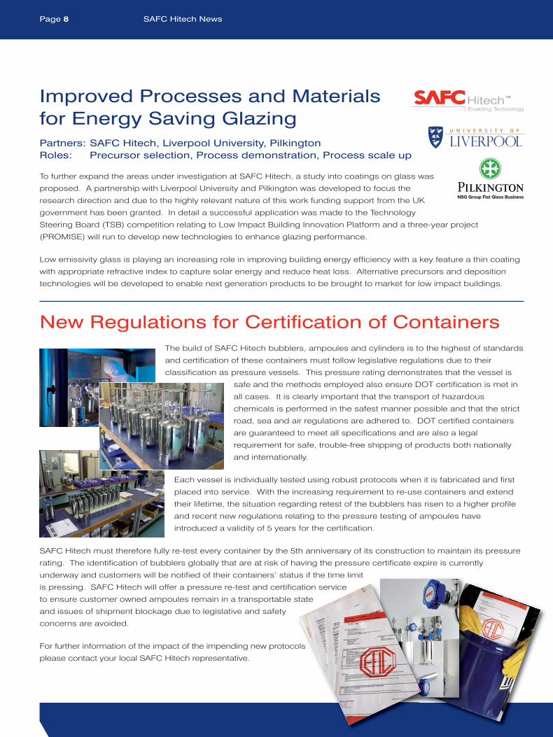
New Regulations for Certification of ContainersThe build of SAFC Hitech bubblers, ampoules and cylinders is to the highest of standards
and certification of these containers must follow legislative regulations due to their
classification as pressure vessels. This pressure rating demonstrates that the vessel is
safe and the methods employed also ensure DOT certification is met in
all cases. It is clearly important that the transport of hazardous
chemicals is performed in the safest manner possible and that the strict
road, sea and air regulations are adhered to. DOT certified containers
are guaranteed to meet all specifications and are also a legal
requirement for safe, trouble-free shipping of products both nationally
and internationally.
Each vessel is individually tested using robust protocols when it is fabricated and first
placed into service. With the increasing requirement to re-use containers and extend
their lifetime, the situation regarding retest of the bubblers has risen to a higher profile
and recent new regulations relating to the pressure testing of ampoules have
introduced a validity of 5 years for the certification.
SAFC Hitech must therefore fully re-test every container by the 5th anniversary of its construction to maintain its pressure
rating. The identification of bubblers globally that are at risk of having the pressure certificate expire is currently
underway and customers will be notified of their containers’ status if the time limit
is pressing. SAFC Hitech will offer a pressure re-test and certification service
to ensure customer owned ampoules remain in a transportable state
and issues of shipment blockage due to legislative and safety
concerns are avoided.
For further information of the impact of the impending new protocols
please contact your local SAFC Hitech representative.
To further expand the areas under investigation at SAFC Hitech, a study into coatings on glass was
proposed. A partnership with Liverpool University and Pilkington was developed to focus the
research direction and due to the highly relevant nature of this work funding support from the UK
government has been granted. In detail a successful application was made to the Technology
Steering Board (TSB) competition relating to Low Impact Building Innovation Platform and a three-year project
(PROMISE) will run to develop new technologies to enhance glazing performance.
Low emissivity glass is playing an increasing role in improving building energy efficiency with a key feature a thin coating
with appropriate refractive index to capture solar energy and reduce heat loss. Alternative precursors and deposition
technologies will be developed to enable next generation products to be brought to market for low impact buildings.
Partners: SAFC Hitech, Liverpool University, PilkingtonRoles: Precursor selection, Process demonstration, Process scale up
Page 9
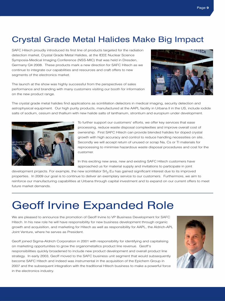
Crystal Grade Metal Halides Make Big ImpactSAFC Hitech proudly introduced its first line of products targeted for the radiation
detection market, Crystal Grade Metal Halides, at the IEEE Nuclear Science
Symposia-Medical Imaging Conference (NSS-MIC) that was held in Dresden,
Germany Q4 2008. These products mark a new direction for SAFC Hitech as we
continue to integrate our capabilities and resources and craft offers to new
segments of the electronics market.
The launch at the show was highly successful from the perspectives of sales
performance and branding with many customers visiting our booth for information
on the new product range.
The crystal grade metal halides find applications as scintillation detectors in medical imaging, security detection and
astrophysical equipment. Our high purity products, manufactured at the AAPL facility in Urbana Il in the US, include iodide
salts of sodium, cesium and thallium with new halide salts of lanthanum, strontium and europium under development.
To further support our customers’ efforts, we offer key services that ease
processing, reduce waste disposal complexities and improve overall cost of
ownership. First SAFC Hitech can provide blended halides for doped crystal
growth with high accuracy and control to reduce handling necessities on site.
Secondly we will accept return of unused or scrap Na, Cs or Tl materials for
reprocessing to minimise hazardous waste disposal procedures and cost for the
customer.
In this exciting new area, new and existing SAFC Hitech customers have
approached us for material supply and invitations to participate in joint
development projects. For example, the new scintillator SrI2:Eu has gained significant interest due to its improved
properties. In 2009 our goal is to continue to deliver an exemplary service to our customers. Furthermore, we aim to
reinforce our manufacturing capabilities at Urbana through capital investment and to expand on our current offers to meet
future market demands.
Geoff Irvine Expanded RoleWe are pleased to announce the promotion of Geoff Irvine to VP Business Development for SAFC
Hitech. In his new role he will have responsibility for new business development through organic
growth and acquisition, and marketing for Hitech as well as responsibility for AAPL, the Aldrich-APL
Joint Venture, where he serves as President.
Geoff joined Sigma-Aldrich Corporation in 2001 with responsibility for identifying and capitalising
on marketing opportunities to grow the organometallics product line revenue. Geoff’s
responsibilities quickly broadened to include new product development and overall product line
strategy. In early 2003, Geoff moved to the SAFC business unit segment that would subsequently
become SAFC Hitech and indeed was instrumental in the acquisition of the Epichem Group in
2007 and the subsequent integration with the traditional Hitech business to make a powerful force
in the electronics industry.
Cadmium Oxide as an Alternative TCOTransparent conducting oxides (TCOs) have found use in a broad array of applications including photovoltaic (PV) cells,
flat panel displays, and light emitting diodes. The dominant material system currently is indium tin oxide (ITO), however,
alternatives are being sought due to the price and availability of In. Face-centred cubic cadmium oxide has a relatively
low intrinsic band gap of 2.28 eV, while its low effective carrier mass allows for heavily doped samples which can have
band gaps as high as 3.35 eV. Sn-doped CdO has been shown to allow access to mobilities of 607 cm2 V-1 s-1 [1]
making it suitable for a large number of TCO applications.
CVD is particularly attractive for TCO synthesis because of its use in conformal, large volume, thin film manufacturing
processes. A key prerequisite for CVD is a volatile precursor and at present only a limited number of examples are
available. Historically, CdO films have been grown via CVD using the combination of dimethylcadmium as a precursor
and butanol as an oxygen source [2]. This dual-source approach leads, naturally, to speculation as to the likelihood of
organocadmium alkoxides as intermediates in this process, and thus such species would be potential single-source
precursors (SSP) in their own right. Indeed, work on the analogous ZnO process identified MeZn(OiPr) as just such an
SSP. [3]
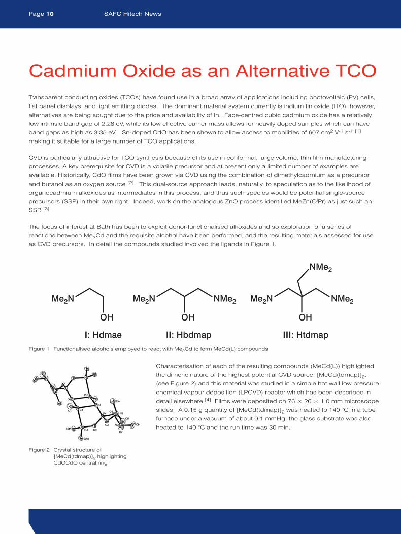
The focus of interest at Bath has been to exploit donor-functionalised alkoxides and so exploration of a series of
reactions between Me2Cd and the requisite alcohol have been performed, and the resulting materials assessed for use
as CVD precursors. In detail the compounds studied involved the ligands in Figure 1.
Page 10 SAFC Hitech News
Me2N
OH
Me2N
OH
NMe2 Me2N
OH
NMe2
NMe2
I: Hdmae II: Hbdmap III: HtdmapFigure 1 Functionalised alcohols employed to react with Me2Cd to form MeCd(L) compounds
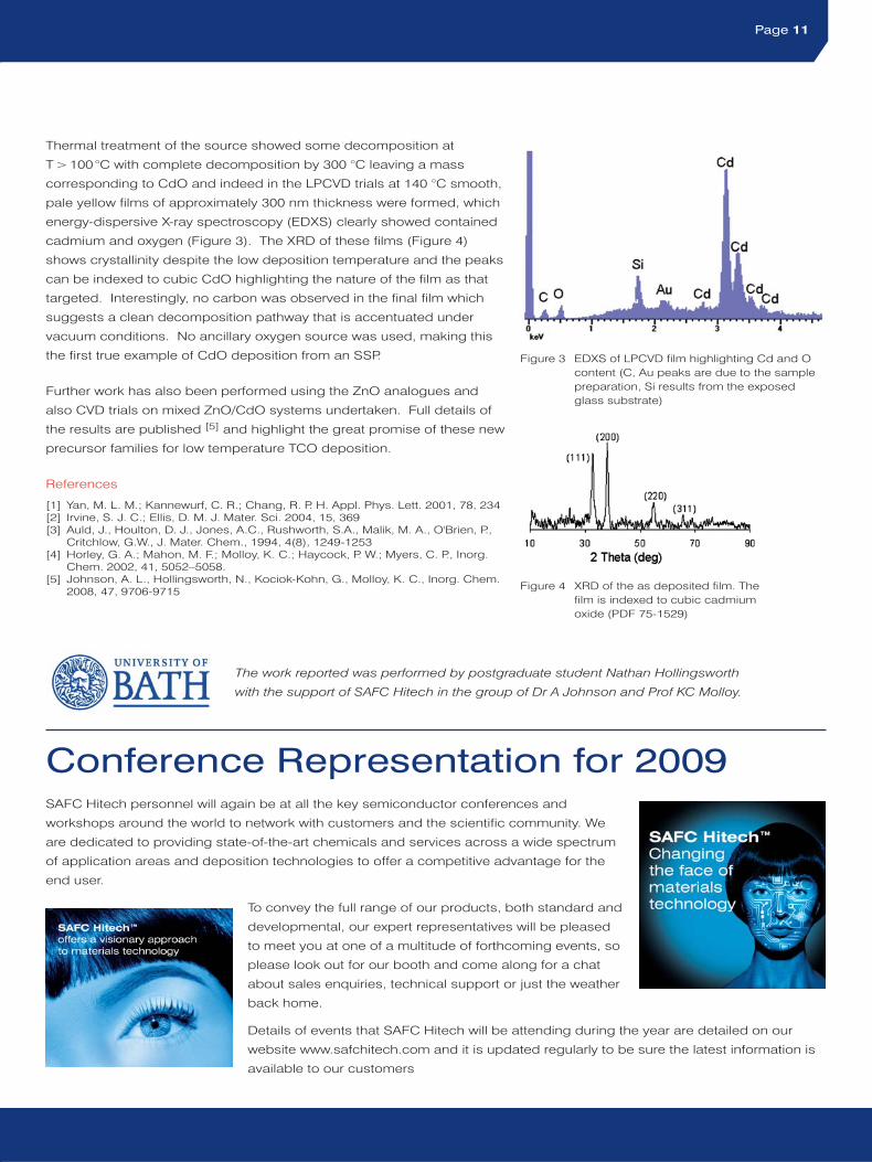
Characterisation of each of the resulting compounds (MeCd(L)) highlighted
the dimeric nature of the highest potential CVD source, [MeCd(tdmap)]2,
(see Figure 2) and this material was studied in a simple hot wall low pressure
chemical vapour deposition (LPCVD) reactor which has been described in
detail elsewhere.[4] Films were deposited on 76 × 26 × 1.0 mm microscope
slides. A 0.15 g quantity of [MeCd(tdmap)]2 was heated to 140 °C in a tube
furnace under a vacuum of about 0.1 mmHg; the glass substrate was also
heated to 140 °C and the run time was 30 min.
Figure 2 Crystal structure of[MeCd(tdmap)]2 highlightingCdOCdO central ring
Page 11
Thermal treatment of the source showed some decomposition at
T>100 °C with complete decomposition by 300 °C leaving a mass
corresponding to CdO and indeed in the LPCVD trials at 140 °C smooth,
pale yellow films of approximately 300 nm thickness were formed, which
energy-dispersive X-ray spectroscopy (EDXS) clearly showed contained
cadmium and oxygen (Figure 3). The XRD of these films (Figure 4)
shows crystallinity despite the low deposition temperature and the peaks
can be indexed to cubic CdO highlighting the nature of the film as that
targeted. Interestingly, no carbon was observed in the final film which
suggests a clean decomposition pathway that is accentuated under
vacuum conditions. No ancillary oxygen source was used, making this
the first true example of CdO deposition from an SSP.
Further work has also been performed using the ZnO analogues and
also CVD trials on mixed ZnO/CdO systems undertaken. Full details of
the results are published [5] and highlight the great promise of these new
precursor families for low temperature TCO deposition.
References
[1] Yan, M. L. M.; Kannewurf, C. R.; Chang, R. P. H. Appl. Phys. Lett. 2001, 78, 234[2] Irvine, S. J. C.; Ellis, D. M. J. Mater. Sci. 2004, 15, 369[3] Auld, J., Houlton, D. J., Jones, A.C., Rushworth, S.A., Malik, M. A., O'Brien, P.,
Critchlow, G.W., J. Mater. Chem., 1994, 4(8), 1249-1253[4] Horley, G. A.; Mahon, M. F.; Molloy, K. C.; Haycock, P. W.; Myers, C. P., Inorg.
Chem. 2002, 41, 5052–5058.[5] Johnson, A. L., Hollingsworth, N., Kociok-Kohn, G., Molloy, K. C., Inorg. Chem.
2008, 47, 9706-9715
Conference Representation for 2009SAFC Hitech personnel will again be at all the key semiconductor conferences and
workshops around the world to network with customers and the scientific community. We
are dedicated to providing state-of-the-art chemicals and services across a wide spectrum
of application areas and deposition technologies to offer a competitive advantage for the
end user.
To convey the full range of our products, both standard and
developmental, our expert representatives will be pleased
to meet you at one of a multitude of forthcoming events, so
please look out for our booth and come along for a chat
about sales enquiries, technical support or just the weather
back home.
Details of events that SAFC Hitech will be attending during the year are detailed on our
website www.safchitech.com and it is updated regularly to be sure the latest information is
available to our customers
Figure 4 XRD of the as deposited film. Thefilm is indexed to cubic cadmiumoxide (PDF 75-1529)
Figure 3 EDXS of LPCVD film highlighting Cd and Ocontent (C, Au peaks are due to the samplepreparation, Si results from the exposedglass substrate)
The work reported was performed by postgraduate student Nathan Hollingsworth
with the support of SAFC Hitech in the group of Dr A Johnson and Prof KC Molloy.

LHV
05340 - 508590
0039
© 2009 SAFC
All rights reserved. Reproduction forbidden without permission.
SAFC Hitech®, SAFC® and Sigma-Aldrich® are registered trademarks of
Sigma-Aldrich Biotechnology L.P. and Sigma-Aldrich Co.
United Kingdom SAFC Hitech, Power Road, Bromborough, Wirral,CH62 3QF Tel: +44 (0) 151 334 2774 Fax: +44 (0) 151 334 6422
United States SAFC Hitech, 1429 Hilldale Ave, Haverhill,Massachusetts, 01832-1300, USA Tel: 610 706 0606 Fax: 610 706 0888
Japan Daido Air Products Electronics Inc, 6-17-17,Shinbashi, Minato-Ku, Tokyo, 105 0004 Japan Tel: +81 3 3432 7032 Fax: +81 3 3578 7827
China SAFC Hitech, Block 8, Room 803, Mandarine City,HongXu Road, No 788, Shanghai, China, 201103 Tel: +86 21 6446 1686 Fax: +86 21 6405 4343
Korea Doje Corporation, 211-2 SongJeong-Dong,GwangJu, GyungGi-do 464-903 Korea Tel: +82 31 764 4907 Fax: +82 31 764 4961
Singapore DNIV, 10 Ang Mo Kio Street 65, #03-04,TECHPOINT, 569059, Singapore Tel: +65 6 483 3386 Fax: +65 6 483 2698
Taiwan SAFC Hitech, 10F No.28 Sec 3, Nan King EastRoad, Taipei 104, Taiwan Tel: +88 62 2509 1399 Fax: +88 62 2501 6279
Europe Fab Support AB, Dovregatan 18, SE-164 36 Kista,Sweden Tel: +46 (0) 8 5620 3330 Fax: +46 (0) 8 5716 2850
www.safchitech.com
Page 12 SAFC Hitech News
SAFC Hitech International Sites
Global email: [email protected]