S3C2440A - Keil · Samsung assumes no responsibility, ... S3C2440A Special Registers ... 2048 Byte...
596
S3C2440A 32-BIT CMOS MICROCONTROLLER USER'S MANUAL Revision 1
Transcript of S3C2440A - Keil · Samsung assumes no responsibility, ... S3C2440A Special Registers ... 2048 Byte...

S3C2440A
32-BIT CMOS
MICROCONTROLLER
USER'S MANUAL
Revision 1

Important Notice
The information in this publication has been carefullychecked and is believed to be entirely accurate at thetime of publication. Samsung assumes noresponsibility, however, for possible errors oromissions, or for any consequences resulting fromthe use of the information contained herein.
Samsung reserves the right to make changes in itsproducts or product specifications with the intent toimprove function or design at any time and withoutnotice and is not required to update thisdocumentation to reflect such changes.
This publication does not convey to a purchaser ofsemiconductor devices described herein any licenseunder the patent rights of Samsung or others.
Samsung makes no warranty, representation, orguarantee regarding the suitability of its products forany particular purpose, nor does Samsung assumeany liability arising out of the application or use of anyproduct or circuit and specifically disclaims any andall liability, including without limitation anyconsequential or incidental damages.
"Typical" parameters can and do vary in differentapplications. All operating parameters, including"Typicals" must be validated for each customerapplication by the customer's technical experts.
Samsung products are not designed, intended, orauthorized for use as components in systemsintended for surgical implant into the body, for otherapplications intended to support or sustain life, or forany other application in which the failure of theSamsung product could create a situation wherepersonal injury or death may occur.
Should the Buyer purchase or use a Samsungproduct for any such unintended or unauthorizedapplication, the Buyer shall indemnify and holdSamsung and its officers, employees, subsidiaries,affiliates, and distributors harmless against all claims,costs, damages, expenses, and reasonable attorneyfees arising out of, either directly or indirectly, anyclaim of personal injury or death that may beassociated with such unintended or unauthorized use,even if such claim alleges that Samsung wasnegligent regarding the design or manufacture of saidproduct.
S3C2440A 32-Bit CMOS MicrocontrollerUser's Manual, Revision 1Publication Number: 21-S3-C2440A-072004
© 2004 Samsung Electronics
All rights reserved. No part of this publication may be reproduced, stored in a retrieval system, or transmitted in anyform or by any means, electric or mechanical, by photocopying, recording, or otherwise, without the prior writtenconsent of Samsung Electronics.
Samsung Electronics' microcontroller business has been awarded full ISO-14001certification (BVQ1 Certificate No. 9330). All semiconductor products are designed andmanufactured in accordance with the highest quality standards and objectives.
Samsung Electronics Co., Ltd.San #24 Nongseo-Ri, Giheung- EupYongin-City, Gyeonggi-Do, KoreaC.P.O. Box #37, Suwon 449-900
TEL: (82)-(031)-209-1490FAX: (82) (331) 209-1909Home-Page URL: Http://www.samsungsemi.com/
Printed in the Republic of Korea
S3C2440A MICROCONTROLLER iii
Table of Contents
Chapter 1 Product Overview
Introduction.........................................................................................................................................1-1Features .............................................................................................................................................1-2Block Diagram ....................................................................................................................................1-5Pin Assignments.................................................................................................................................1-6Signal Descriptions..............................................................................................................................1-20S3C2440A Special Registers................................................................................................................1-26
Chapter 2 Programmer's Model
Overview.............................................................................................................................................2-1Processor Operating States .........................................................................................................2-1Switching State...........................................................................................................................2-1Memory Formats.........................................................................................................................2-1Big-Endian Format.......................................................................................................................2-2Little-Endian Format ....................................................................................................................2-2Instruction Length........................................................................................................................2-2Operating Modes .........................................................................................................................2-3Registers ....................................................................................................................................2-3The Program Status Registers ......................................................................................................2-7Exceptions .................................................................................................................................2-10Interrupt Latencies .......................................................................................................................2-15Reset .........................................................................................................................................2-15
iv S3C2440A MICROCONTROLLER
Table of Contents (Continued)
Chapter 3 ARM Instruction Set
Instruction Set Summay.......................................................................................................................3-1Format Summary ........................................................................................................................3-1Instruction Summary....................................................................................................................3-2
The Condition Field..............................................................................................................................3-4Branch and Exchange (Bx)...................................................................................................................3-5
Instruction Cycle Times................................................................................................................3-5Assembler Syntax .......................................................................................................................3-5Using R15 as an Operand ............................................................................................................3-5
Branch and Branch with Link (B, Bl)......................................................................................................3-7The Link Bit ................................................................................................................................3-7Instruction Cycle Times................................................................................................................3-7Assembler Syntax .......................................................................................................................3-8
Data Processing..................................................................................................................................3-9Cpsr Flags ..................................................................................................................................3-11Shifts .........................................................................................................................................3-12Immediate Operand Rotates .........................................................................................................3-16Writing to R15.............................................................................................................................3-16Using R15 as an Operandy...........................................................................................................3-16TEQ, TST, Cmp and Cmn Opcodes...............................................................................................3-16Instruction Cycle Times................................................................................................................3-16Assembler Syntax .......................................................................................................................3-17Examples ...................................................................................................................................3-17
Psr Transfer (MRS, MSR).....................................................................................................................3-18Operand Restrictions ...................................................................................................................3-18Reserved Bits..............................................................................................................................3-20Examples ...................................................................................................................................3-20Instruction Cycle Times................................................................................................................3-20Assembly Syntax ........................................................................................................................3-21Examples ...................................................................................................................................3-21
Multiply And Multiply-Accumulate (MUL, MLA).......................................................................................3-22Cpsr Flags ..................................................................................................................................3-24Instruction Cycle Times................................................................................................................3-24Assembler Syntax .......................................................................................................................3-24Examples ...................................................................................................................................3-24
Multiply Long And Multiply-Accumulate Long (MULL, MLAL) ...................................................................3-25Operand Restrictions ...................................................................................................................3-26Cpsr Flags ..................................................................................................................................3-26Instruction Cycle Times................................................................................................................3-26Assembler Syntax .......................................................................................................................3-27Examples ...................................................................................................................................3-27

S3C2440A MICROCONTROLLER v
Table of Contents (Continued)
Chapter 3 ARM Instruction Set (Continued)
Single Data Transfer (LDR, STR)...........................................................................................................3-28Offsets and Auto-Indexing ............................................................................................................3-29Shifted Register Offset .................................................................................................................3-29Bytes and Words ........................................................................................................................3-29Use of R15..................................................................................................................................3-31Example.....................................................................................................................................3-31Data Aborts ................................................................................................................................3-31Instruction Cycle Times................................................................................................................3-31Assembler Syntax .......................................................................................................................3-32Examples ...................................................................................................................................3-33
Halfword and Signed Data Transfer (LDRH/STRH/LDRSB/LDRSH) ...........................................................3-34Offsets and Auto-Indexing ............................................................................................................3-35Halfword Load and Stores.............................................................................................................3-36Use of R15..................................................................................................................................3-37Data Aborts ................................................................................................................................3-37Instruction Cycle Times................................................................................................................3-37Assembler Syntax .......................................................................................................................3-38Examples ...................................................................................................................................3-39
Block Data Transfer (LDM, STM)...........................................................................................................3-40The Register List .........................................................................................................................3-40Addressing Modes.......................................................................................................................3-41Address Alignment ......................................................................................................................3-41Use of the S Bit...........................................................................................................................3-43Use of R15 as The Base ..............................................................................................................3-43Inclusion of the Base in the Register List .......................................................................................3-44Data Aborts ................................................................................................................................3-44Instruction Cycle Times................................................................................................................3-44Assembler Syntax .......................................................................................................................3-45Examples ...................................................................................................................................3-46
Single Data Swap (SWP).....................................................................................................................3-47Bytes and Words ........................................................................................................................3-47Use of R15..................................................................................................................................3-48Data Aborts ................................................................................................................................3-48Instruction Cycle Times................................................................................................................3-48Assembler Syntax .......................................................................................................................3-48
Software Interrupt (SWI) .......................................................................................................................3-49Return from the Supervisor ...........................................................................................................3-49Comment Field............................................................................................................................3-49Instruction Cycle Times................................................................................................................3-49Assembler Syntax .......................................................................................................................3-50
Coprocessor Data Operations (CDP).....................................................................................................3-51Coprocessor Instructions..............................................................................................................3-51Instruction Cycle Times................................................................................................................3-52Examples ...................................................................................................................................3-52
vi S3C2440A MICROCONTROLLER
Table of Contents (Continued)
Chapter 3 ARM Instruction Set (Continued)
Coprocessor Data Transfers (LDC, STC)................................................................................................3-53The Coprocessor Fields ...............................................................................................................3-54Addressing Modes.......................................................................................................................3-54Address Alignment ......................................................................................................................3-54Data Aborts ................................................................................................................................3-54Assembler Syntax .......................................................................................................................3-55Examples ...................................................................................................................................3-55Coprocessor Register Transfers (MRC, MCR).................................................................................3-56The Coprocessor Fields ...............................................................................................................3-56Transfers to R15..........................................................................................................................3-57Transfers from R15 ......................................................................................................................3-57Instruction Cycle Times................................................................................................................3-57Assembler Syntax .......................................................................................................................3-57Examples ...................................................................................................................................3-57Undefined Instruction ...................................................................................................................3-58Instruction Cycle Times................................................................................................................3-58Assembler Syntax .......................................................................................................................3-58Instruction Set Examples .............................................................................................................3-59Using the Conditional Instructions .................................................................................................3-59Pseudo-Random Binary Sequence Generator.................................................................................3-61Multiplication by Constant Using the Barrel Shifter..........................................................................3-61Loading a Word from an Unknown Alignment .................................................................................3-63
Chapter 4 Thumb Instruction Set
Thumb Instruction Set Format...............................................................................................................4-1Format Summary ........................................................................................................................4-2Opcode Summary .......................................................................................................................4-3
Format 1: Move Shifted Register ...........................................................................................................4-5Operation....................................................................................................................................4-5Instruction Cycle Times................................................................................................................4-6Examples ...................................................................................................................................4-6
Format 2: Add/Subtract........................................................................................................................4-7Operation....................................................................................................................................4-7Instruction Cycle Times................................................................................................................4-8Examples ...................................................................................................................................4-8
Format 3: Move/Compare/Add/Subtract Immediate.................................................................................4-9Operations ..................................................................................................................................4-9Instruction Cycle Times................................................................................................................4-10Examples ...................................................................................................................................4-10

S3C2440A MICROCONTROLLER vii
Table of Contents (Continued)
Chapter 4 Thumb Instruction Set (Continued)
Format 4: ALU Operations....................................................................................................................4-11Operation....................................................................................................................................4-11Instruction Cycle Times................................................................................................................4-12Examples ...................................................................................................................................4-12
Format 5: Hi-Register Operations/Branch Exchange ...............................................................................4-13Operation....................................................................................................................................4-13Instruction Cycle Times................................................................................................................4-14The BX Instruction .......................................................................................................................4-14Examples ...................................................................................................................................4-15Using R15 As an Operand............................................................................................................4-15
Format 6: PC-Relative Load..................................................................................................................4-16Operation....................................................................................................................................4-16Instruction Cycle Times................................................................................................................4-17Examples ...................................................................................................................................4-17
Format 7: Load/Store With Register Offset.............................................................................................4-18Operation....................................................................................................................................4-19Instruction Cycle Times................................................................................................................4-19Examples ...................................................................................................................................4-19
Format 8: Load/Store Sign-Extended Byte/Halfword................................................................................4-20Operation....................................................................................................................................4-20Instruction Cycle Times................................................................................................................4-21Examples ...................................................................................................................................4-21
Format 9: Load/Store With Immediate Offset..........................................................................................4-22Operation....................................................................................................................................4-23Instruction Cycle Times................................................................................................................4-23Examples ...................................................................................................................................4-23
Format 10: Load/Store Halfword............................................................................................................4-24Operation....................................................................................................................................4-24Examples ...................................................................................................................................4-25
Format 11: SP-Relative Load/Store .......................................................................................................4-26Operation....................................................................................................................................4-26Instruction Cycle Times................................................................................................................4-27Examples ...................................................................................................................................4-27
Format 12: Load Address.....................................................................................................................4-28Operation....................................................................................................................................4-28Instruction Cycle Times................................................................................................................4-29Examples ...................................................................................................................................4-29
Format 13: Add Offset to Stack Pointer .................................................................................................4-30Operation....................................................................................................................................4-30Instruction Cycle Times................................................................................................................4-30Examples ...................................................................................................................................4-30
viii S3C2440A MICROCONTROLLER
Table of Contents (Continued)
Chapter 4 Thumb Instruction Set (Continued)
Format 14: Push/Pop Registers ............................................................................................................4-31Operation....................................................................................................................................4-31Instruction Cycle Times................................................................................................................4-32Examples ...................................................................................................................................4-32
Format 15: Multiple Load/Store.............................................................................................................4-33Operation....................................................................................................................................4-33Instruction Cycle Times................................................................................................................4-33Examples ...................................................................................................................................4-33
Format 16: Conditional Branch..............................................................................................................4-34Operation....................................................................................................................................4-34Instruction Cycle Times................................................................................................................4-35Examples ...................................................................................................................................4-35
Format 17: Software Interrupt................................................................................................................4-36Operation....................................................................................................................................4-36Instruction Cycle Times................................................................................................................4-36Examples ...................................................................................................................................4-36
Format 18: Unconditional Branch..........................................................................................................4-37Operation....................................................................................................................................4-37Examples ...................................................................................................................................4-37
Format 19: long branch with link ...........................................................................................................4-38Operation....................................................................................................................................4-38Instruction Cycle Times................................................................................................................4-39Examples ...................................................................................................................................4-39
Instruction Set Examples .....................................................................................................................4-40Multiplication by A Constant Using Shifts and Adds........................................................................4-40General Purpose Signed Divide.....................................................................................................4-41Division by a Constant .................................................................................................................4-43
S3C2440A MICROCONTROLLER ix
Table of Contents (Continued)
Chapter 5 Memory Controller
Overview.............................................................................................................................................5-1Function Description............................................................................................................................5-4
Bank0 Bus Width........................................................................................................................5-4Memory (SROM/SDRAM) Address Pin Connections.......................................................................5-4Sdram Bank Address Pin Connection Example..............................................................................5-5nWAIT Pin Operation ...................................................................................................................5-6nXBREQ/nXBACK Pin Operation...................................................................................................5-7Programmable Access Cycle .......................................................................................................5-12Bus Width & Wait Control Register (Bwscon).................................................................................5-14Bank Control Register (Bankconn: NGCS0-NGCS5) .......................................................................5-16Bank Control Register (Bankconn: NGCS6-NGCS7) .......................................................................5-17Refresh Control Register ..............................................................................................................5-18Banksize Register .......................................................................................................................5-19Sdram Mode Register Set Register (MRSR)...................................................................................5-20
Chapter 6 Nand Flash Contorller
Overview.............................................................................................................................................6-1Features .....................................................................................................................................6-1Block Diagram ............................................................................................................................6-2Boot Loader Function...................................................................................................................6-2Pin Configuration .........................................................................................................................6-3Nand Flash Memory Configuration Table........................................................................................6-3Nand Flash Memory Timing..........................................................................................................6-4
Software Mode ....................................................................................................................................6-5Steppingstone (4K-Byte SRAM)....................................................................................................6-6
Ecc (Error Correction Code)..................................................................................................................6-72048 Byte ECC Parity Code Assignment Table ..............................................................................6-716 Byte ECC Parity Code Assignment Table..................................................................................6-7ECC Module Features..................................................................................................................6-8ECC Programming Guide .............................................................................................................6-8Nand Flash Memory Mapping .......................................................................................................6-9Nand Flash Memory Configuration.................................................................................................6-10Nand Flash Configuration Register ................................................................................................6-12Control Register ..........................................................................................................................6-13Command Register......................................................................................................................6-15Address Register.........................................................................................................................6-15Data Register..............................................................................................................................6-15Main Data Area Register ..............................................................................................................6-16Spare Area Ecc Register.............................................................................................................6-17NFCON Status Register...............................................................................................................6-18ECC0/1 Status Register...............................................................................................................6-19Main Data Area ECC0 Status Register ..........................................................................................6-20Spare Area ECC Status Register ..................................................................................................6-20Block Address Register ...............................................................................................................6-21
x S3C2440A MICROCONTROLLER
Table of Contents (Continued)
Chapter 7 Clock & Power Management
Overview.............................................................................................................................................7-1Functional Description .........................................................................................................................7-2
Clock Architecture.......................................................................................................................7-2Clock Source Selection................................................................................................................7-2Phase Locked Loop (PLL) ............................................................................................................7-4Clock Control Logic .....................................................................................................................7-6Power Management .....................................................................................................................7-10
Clock Generator & Power Management Special Register ........................................................................7-20Lock Time Count Register (LOCKTIME).........................................................................................7-20PLL Control Register (MPLLCON & UPLLCON)..............................................................................7-21PLL Value Selection Table ...........................................................................................................7-21Clock Control Register (CLKCON).................................................................................................7-22Clock Slow Control (CLKSLOW) Register ......................................................................................7-23Clock Divider Control (CLKDIVN) Register......................................................................................7-24Camera Clock Divider (CAMDIVN) Register....................................................................................7-25
Chapter 8 DMA
Overview.............................................................................................................................................8-1DMA Request Sources ........................................................................................................................8-2DMA Operation ...................................................................................................................................8-2
External DMA DREQ/DACK Protocol ............................................................................................8-3Examples ...........................................................................................................................................8-6DMA Special Registers ........................................................................................................................8-7
DMA Initial Source (DISRC) Register.............................................................................................8-7DMA Initial Source Control (DISRCC) Register ...............................................................................8-7DMA Initial Destination (DIDST) Register .......................................................................................8-8DMA Initial Destination Control (DIDSTC) Register..........................................................................8-8DMA Control (DCON) Register......................................................................................................8-9DMA Status (DSTAT) Register......................................................................................................8-12DMA Current Source (DCSRC) Register ........................................................................................8-13Current Destination (DCDST) Register ...........................................................................................8-13DMA Mask Trigger (DMASKTRIG) Register....................................................................................8-14

S3C2440A MICROCONTROLLER xi
Table of Contents (Continued)
Chapter 9 I/O PORTS
Overview.............................................................................................................................................9-1Port Control Descriptions .....................................................................................................................9-7
Port Configuration Register (GPACON-GPJCON)............................................................................9-7Port Data Register (GPADAT-GPJDAT) .........................................................................................9-7Port Pull-Up Register (GPBUP-GPJUP).........................................................................................9-7Miscellaneous Control Register.....................................................................................................9-7External Interrupt Control Register.................................................................................................9-7
I/O Port Control Register ......................................................................................................................9-8Port A Control Registers (GPACON, GPADAT) ..............................................................................9-8Port B Control Registers (GPBCON, GPBDAT, GPBUP).................................................................9-10Port C Control Registers (GPCCON, GPCDAT, GPCUP).................................................................9-11Port D Control Registers (GPDCON, GPDDAT, GPDUP).................................................................9-13Port E Control Registers (GPECON, GPEDAT, GPEUP).................................................................9-15Port F Control Registers (GPFCON, GPFDAT) ...............................................................................9-17Port G Control Registers (GPGCON, GPGDAT) .............................................................................9-18Port H Control Registers (GPHCON, GPHDAT) ..............................................................................9-20Port J Control Registers (GPJCON, GPJDAT) ................................................................................9-21Miscellaneous Control Register (MISCCR) .....................................................................................9-23DCLK Control Registers (DCLKCON).............................................................................................9-25EXTINTn (External Interrupt Control Register n)...............................................................................9-26EINTFLTn (External Interrupt Filter Register n)................................................................................9-30EINTMASK (External Interrupt Mask Register) ...............................................................................9-31EINTPEND (External Interrupt Pending Register) ............................................................................9-32GSTATUSn (General Status Registers) .........................................................................................9-33DSCn (Drive Strength Control).......................................................................................................9-34DSCn (Drive Strength Control).......................................................................................................9-35MSLCON (Memory Sleep Control Register)....................................................................................9-36

xii S3C2440A MICROCONTROLLER
Table of Contents (Continued)
Chapter 10 Basic Timer
Overview.............................................................................................................................................10-1Feature.......................................................................................................................................10-1
PWM Timer Operation .........................................................................................................................10-3Prescaler & Divider ......................................................................................................................10-3Basic Timer Operation .................................................................................................................10-3Auto Reload & Double Buffering ....................................................................................................10-4Timer Initialization Using Manual Update Bit and Inverter Bit ............................................................10-5Timer Operation...........................................................................................................................10-6Pulse Width Modulation (PWM)....................................................................................................10-7Output Level Control ....................................................................................................................10-8Dead Zone Generator...................................................................................................................10-9DMA Request Mode ....................................................................................................................10-10
PWM Timer Control Registers ..............................................................................................................10-11Timer Configuration Register0 (TCFG0)..........................................................................................10-11Timer Configuration Register1 (TCFG1)..........................................................................................10-12Timer Control (TCON) Register......................................................................................................10-13Timer 0 Count Buffer Register & Compare Buffer Register (TCNTB0/TCMPB0)...................................10-15Timer 0 Count Observation Register (TCNTO0) ...............................................................................10-15Timer 1 Count Buffer Register & Compare Buffer Register (TCNTB1/TCMPB1)...................................10-16Timer 1 Count Observation Register (TCNTO1) ...............................................................................10-16Timer 2 Count Buffer Register & Compare Buffer Register (TCNTB2/TCMPB2)...................................10-17Timer 2 Count Observation Register (TCNTO2) ...............................................................................10-17Timer 3 Count Buffer Register & Compare Buffer Register (TCNTB3/TCMPB3)...................................10-18Timer 3 Count Observation Register (TCNTO3) ...............................................................................10-18Timer 4 Count Buffer Register (TCNTB4) ........................................................................................10-19Timer 4 Count Observation Register (TCNTO4) ...............................................................................10-19
S3C2440A MICROCONTROLLER xiii
Table of Contents (Continued)
Chapter 11 UART
Overview.............................................................................................................................................11-1Features .....................................................................................................................................11-1
Block Diagram ....................................................................................................................................11-2Uart Operation.............................................................................................................................11-3
Uart Special Registers .........................................................................................................................11-10Uart Line Control Register ............................................................................................................11-10Uart Control Register ...................................................................................................................11-11Uart FIFO Control Register ...........................................................................................................11-14Uart Modem Control Register........................................................................................................11-15Uart Tx/Rx Status Register...........................................................................................................11-16Uart Error Status Register ............................................................................................................11-17Uart FIFO Status Register............................................................................................................11-18Uart Modem Status Register ........................................................................................................11-19Uart Transmit Buffer Register (HOLDING Register & FIFO Register) .................................................11-20Uart Receive Buffer Register (HOLDING Register & FIFO Register) ..................................................11-20Uart Baud Rate Divisor Register....................................................................................................11-21
Chapter 12 USB HOST Controller
Overview.............................................................................................................................................12-1Usb Host Controller Special Registers ...................................................................................................12-2
OHCI Registers for Usb Host Controller .........................................................................................12-2

xiv S3C2440A MICROCONTROLLER
Table of Contents (Continued)
Chapter 13 USB Device Controller
Overview.............................................................................................................................................13-1Feature.......................................................................................................................................13-1
Usb Device Controller Special Registers ................................................................................................13-3Function Address Register (FUNC_ADDR_REG)............................................................................13-5Power Management Register (PWR_REG) ....................................................................................13-6Interrupt Register (EP_INT_REG/USB_INT_REG) ...........................................................................13-7Interrupt Enable Register (EP_INT_EN_REG/USB_INT_EN_REG)....................................................13-9Frame Number Register (FPAME_NUM1_REG/FRAME_NUM2_REG) .............................................13-10Index Register (INDEX_REG)........................................................................................................13-11MAX Packet Register (MAXP_REG)..............................................................................................13-11END Point0 Control Status Register (EP0_CSR) ............................................................................13-12END Point In Control Status Register (IN_CSR1_REG/IN_CSR2_REG) ............................................13-13END Point Out Control Status Register (OUT_CSR1_REG/OUT_CSR2_REG) ..................................13-15END Point Out Write Count Register (OUT_FIFO_CNT1_REG/OUT_FIFO_CNT2_REG).....................13-17END Point FIFO Register (EPN_FIFO_REG)..................................................................................13-17DMA Interface Control Register (EPN_DMA_CON) .........................................................................13-18DMA Unit Counter Register (EPN_DMA_UNIT) ...............................................................................13-19DMA FIFO Counter Register (EPN_DMA_FIFO) .............................................................................13-20DMA Total Transfer Counter Register (EPn_DMA_TTC_L, M, H) ......................................................13-21
Chapter 14 Interrupt Controller
Overview.............................................................................................................................................14-1Interrupt Controller Operation ........................................................................................................14-2Interrupt Sources .........................................................................................................................14-3Interrupt Sub Sources ..................................................................................................................14-4Interrupt Priority Generating Block.................................................................................................14-5Interrupt Priority...........................................................................................................................14-6
Interrupt Controller Special Registers.....................................................................................................14-7Source Pending (SRCPND) Register .............................................................................................14-7Interrupt Mode (INTMOD) Register.................................................................................................14-9Interrupt Mask (INTMSK) Register.................................................................................................14-11Priority Register (PRIORITY).........................................................................................................14-13Interrupt Pending (INTPND) Register..............................................................................................14-14Interrupt Offset (INTOFFSET) Register...........................................................................................14-16Sub Source Pending (SUBSRCPND) Register................................................................................14-17Interrupt Sub Mask (INTSUBMSK) Register ...................................................................................14-18
S3C2440A MICROCONTROLLER xv
Table of Contents (Continued)
Chapter 15 LCD Controller
Overview.............................................................................................................................................15-1Features .....................................................................................................................................15-1Common Features .......................................................................................................................15-2External Interface Signal ..............................................................................................................15-2Block Diagram ............................................................................................................................15-3
STN LCD Controller Operation ..............................................................................................................15-4Timing Generator (TIMEGEN) .......................................................................................................15-4Video Operation ..........................................................................................................................15-5Dithering and Frame Rate Control .................................................................................................15-7Memory Data Format (STN, BSWP = 0)........................................................................................15-9
TFT LCD Controller Operation ...............................................................................................................15-16Video Operation ..........................................................................................................................15-16Memory Data Format (TFT) ..........................................................................................................15-17256 Palette Usage (TFT) ..............................................................................................................15-21Samsung TFT LCD Panel(3.5” PORTRAIT/256K COLOR/REFLECTIVE A-SI/TRANSFLECTIVE A-SI TFT LCD).........................15-24Virtual Display (TFT/STN).............................................................................................................15-25LCD Power Enable (STN/TFT).......................................................................................................15-26LCD Controller Special Registers ..................................................................................................15-27Frame Buffer Start Address 1 Register ..........................................................................................15-33
Chapter 16 ADC & Touch Screen Interface
Overview.............................................................................................................................................16-1Features .....................................................................................................................................16-1
ADC & Touch Screen Interface Operation ..............................................................................................16-2Block Diagram ............................................................................................................................16-2Function Descriptions ..................................................................................................................16-3
ADC AND Touch Screen Interface Special Registers ..............................................................................16-5ADC Control Register (ADCCON)..................................................................................................16-5ADC Touch Screen Control Register (ADCTSC)..............................................................................16-6ADC Start Delay Register (ADCDLY).............................................................................................16-7ADC Conversion Data Register (ADCDAT0)....................................................................................16-8ADC Conversion Data Register (ADCDAT1)....................................................................................16-9ADC Touch Screen Up-Down INT Check Register (ADCUPDN) ........................................................16-9
xvi S3C2440A MICROCONTROLLER
Table of Contents (Continued)
Chapter 17 Real Time Clock
Overview.............................................................................................................................................17-1Features .....................................................................................................................................17-1Real Time Clock Operation...........................................................................................................17-2Leap Year Generator....................................................................................................................17-2Read/Write Registers...................................................................................................................17-2Backup Battery Operation ............................................................................................................17-2Alarm Function............................................................................................................................17-3TICK Time Interrupt ......................................................................................................................17-332.768kHz X-Tal Connection Example ..........................................................................................17-3
Real Time Clock Special Registers .......................................................................................................17-4Real Time Clock Control (RTCCON) Register .................................................................................17-4TICK Time Count (TICNT) Register ................................................................................................17-4RTC Alarm Control (RTCALM) Register..........................................................................................17-5ALARM Second Data (ALMSEC) Register .....................................................................................17-6ALARM Min Data (ALMMIN) Register............................................................................................17-6ALARM Hour Data (ALMHOUR) Register.......................................................................................17-6ALARM Date Data (ALMDATE) Register........................................................................................17-7ALARM Mon Data (ALMMON) Register .........................................................................................17-7ALARM Year Data (ALMYEAR) Register .......................................................................................17-7BCD Second (BCDSEC) Register .................................................................................................17-8BCD Minute (BCDMIN) Register....................................................................................................17-8BCD Hour (BCDHOUR) Register ...................................................................................................17-8BCD Date (BCDDATE) Register....................................................................................................17-9BCD Day (BCDDAY) Register.......................................................................................................17-9BCD Month (BCDMON) Register...................................................................................................17-9BCD Year (BCDYEAR) Register ...................................................................................................17-10
Chapter 18 Watchdog Timer
Overview.............................................................................................................................................18-1Features .....................................................................................................................................18-1Watchdog Timer Operation...........................................................................................................18-2Wtdat & Wtcnt ............................................................................................................................18-2Consideration of Debugging Environment .......................................................................................18-2
Watchdog Timer Special Registers .......................................................................................................18-3Watchdog Timer Control (WTCON) Register...................................................................................18-3Watchdog Timer Data (WTDAT) Register.......................................................................................18-4Watchdog Timer Count (WTCNT) Register .....................................................................................18-4
S3C2440A MICROCONTROLLER xvii
Table of Contents (Continued)
Chapter 19 MMC/SD/SDIO Controller
Features .............................................................................................................................................19-1Block Diagram ....................................................................................................................................19-1SD Operation ......................................................................................................................................19-2SDIO Operation...................................................................................................................................19-3SDI Special Registers ..........................................................................................................................19-4
SDI Control Register (SDICON).....................................................................................................19-4SDI Baud Rate Prescaler Register (SDIPRE) .................................................................................19-4SDI Command Argument Register (SDICmdArg).............................................................................19-5SDI Command Control Register (SDICmdCon)................................................................................19-5SDI Command Status Register (SDICmdSta) .................................................................................19-6SDI Response Register 0 (SDIRSP0) ............................................................................................19-6SDI Response Register 1 (SDIRSP1) ............................................................................................19-6SDI Response Register 2 (SDIRSP2) ............................................................................................19-7SDI Response Register 3 (SDIRSP3) ............................................................................................19-7SDI Data / Busy Timer Register (SDIDTimer)..................................................................................19-7SDI Block Size Register (SDIBSize)..............................................................................................19-7SDI Data Control Register (SDIDatCon) .........................................................................................19-8SDI Data Remain Counter Register (ADIDatCnt).............................................................................19-9SDI Data Status Register (ADIDatSta)...........................................................................................19-9SDI FIFO Status Register (SDIFSTA)............................................................................................19-10SDI Interrupt Mask Register (SDIIntMsk)........................................................................................19-11SDI Data Register (SDIDAT) .........................................................................................................19-12
Chapter 20 IIC-Bus Interface
Overview.............................................................................................................................................20-1IIC-Bus Interface..........................................................................................................................20-3Start and Stop Conditions ............................................................................................................20-3Data Transfer Format ...................................................................................................................20-4ACK Signal Transmission.............................................................................................................20-5Read-Write Operation ..................................................................................................................20-6Bus Arbitration Procedures...........................................................................................................20-6Abort Conditions..........................................................................................................................20-6Configuring IIC-Bus ......................................................................................................................20-6Flowcharts of Operations in Each Mode.........................................................................................20-7
IIC-Bus Interface Special Registers .......................................................................................................20-11Multi-Master IIC-Bus Control (IICCON) Register ..............................................................................20-11Multi-Master IIC-Bus Control/Status (IICSTAT) Register...................................................................20-12Multi-Master IIC-Bus Address (IICADD) Register.............................................................................20-13Multi-Master IIC-Bus Transmit/Receive Data Shift (IICDS) Register...................................................20-13Multi-Master IIC-Bus Line Contro l(IICLC) Register ..........................................................................20-14
xviii S3C2440A MICROCONTROLLER
Table of Contents (Continued)
Chapter 21 IIS-Bus Interface
Overview.............................................................................................................................................21-1Block Diagram ....................................................................................................................................21-2Functional Descriptions........................................................................................................................21-2
Transmit or Receive Only Mode ....................................................................................................21-2Dma Transfer ..............................................................................................................................21-3Transmit and Receive Mode..........................................................................................................21-3
Audio Serial Interface Format................................................................................................................21-3IIS-Bus Format ............................................................................................................................21-3MSB (Left) Justified .....................................................................................................................21-3Sampling Frequency and Master Clock .........................................................................................21-4
IIS-Bus Interface Special Registers .......................................................................................................21-5IIS Control (IISCON) Register........................................................................................................21-5IIS Mode Register (IISMOD) Register.............................................................................................21-6IIS Prescaler (IISPSR) Register.....................................................................................................21-7IIS FIFO Control (IISFCON) Register..............................................................................................21-8IIS FIFO (IISFIFO) Register...........................................................................................................21-8
Chapter 22 SPI
Overview.............................................................................................................................................22-1Features .....................................................................................................................................22-1Block Diagram ............................................................................................................................22-2
SPI Operation .....................................................................................................................................22-3Programming Procedure...............................................................................................................22-3SPI Transfer Format.....................................................................................................................22-4Transmitting Procedure for DMA ...................................................................................................22-5Receiving Procedure for DMA .......................................................................................................22-5
SPI Special Registers ..........................................................................................................................22-6SPI Control Register ....................................................................................................................22-6SPI Status Register.....................................................................................................................22-7SPI Pin Control Register ..............................................................................................................22-8SPI Baud Rate Prescaler Register ................................................................................................22-9SPI Tx Data Register ...................................................................................................................22-9SPI Rx Data Register...................................................................................................................22-9
S3C2440A MICROCONTROLLER xix
Table of Contents (Continued)
Chapter 23 Camera Interface
Overview.............................................................................................................................................23-1Features .....................................................................................................................................23-1Block Diagram ............................................................................................................................23-2Timing Diagram ...........................................................................................................................23-3
Camera Interface Operation ..................................................................................................................23-5Two DMA Paths ..........................................................................................................................23-5Clock Domain .............................................................................................................................23-5Frame Memory Hirerarchy ............................................................................................................23-6Memory Storing Method...............................................................................................................23-8Timing Diagram for Register Setting ..............................................................................................23-9Timing Diagram for Last IRQ.........................................................................................................23-10
Camera Interface Special Registers.......................................................................................................23-11Source Format Register ...............................................................................................................23-11Window Option Register...............................................................................................................23-12Global Control Register ................................................................................................................23-13Y1 Start Address Register............................................................................................................23-13Y2 Start Address Register............................................................................................................23-13Y3 Start Address Register............................................................................................................23-14Y4 Start Address Register............................................................................................................23-14CB1 Start Address Register .........................................................................................................23-14CB2 Start Address Register .........................................................................................................23-14CB3 Start Address Register .........................................................................................................23-15CB4 Start Address Register .........................................................................................................23-15CR1 Start Address Register .........................................................................................................23-15CR2 Start Address Register .........................................................................................................23-15CR3 Start Address Register .........................................................................................................23-16CR4 Start Address Register .........................................................................................................23-16Codec Target Format Register ......................................................................................................23-17Codec Dma Control Register ........................................................................................................23-19Register Setting Guide for Codec Scaler and Preview Scaler ...........................................................23-20Codec Pre-Scaler Control Register 1.............................................................................................23-21Codec Pre-Scaler Control Register 2.............................................................................................23-21Codec Main-Scaler Control Register..............................................................................................23-22Codec Dma Target Area Register..................................................................................................23-22Codec Status Register.................................................................................................................23-23RGB1 Start Address Register.......................................................................................................23-23RGB2 Start Address Register.......................................................................................................23-23RGB3 Start Address Register.......................................................................................................23-24RGB4 Start Address Register.......................................................................................................23-24Preview Target Format Register ....................................................................................................23-24Preview DMA Control Register ......................................................................................................23-25

xx S3C2440A MICROCONTROLLER
Table of Contents (Continued)
Chapter 23 Camera Interface (Continued)
Preview Pre-Scaler Control Register 1 ...........................................................................................23-25Preview Pre-Scaler Control Register 2 ...........................................................................................23-26Preview Main-Scaler Control Register ............................................................................................23-26Preview DMA Target Area Register................................................................................................23-26Preview Status Register ...............................................................................................................23-27Image Capture Enable Register.....................................................................................................23-27
Chapter 24 AC97 Controller
Overview.............................................................................................................................................24-1Features .....................................................................................................................................24-1
AC97 Controller Operation....................................................................................................................24-2Block Diagram ............................................................................................................................24-2Internal Data Path........................................................................................................................24-3
Operation Flow Chart ...........................................................................................................................24-4AC-Link Digital Interface Protocol..........................................................................................................24-5
AC-Link Output Frame (SDATA_OUT) ...........................................................................................24-6AC-Link Input Frame (SDATA_IN) .................................................................................................24-6
AC97 Powerdown ................................................................................................................................24-7AC97 Controller Special Registers ........................................................................................................24-9
AC97 Global Control Register (AC_GLBCTRL) ...............................................................................24-9AC97 Global Status Register (AC_GLBSTAT) ................................................................................24-10AC97 Codec Command Register (AC_CODEC_CMD).....................................................................24-10AC97 Codec Status Register (AC_CODEC_STAT) .........................................................................24-11AC97 PCM Out/In Channel FIFO Address Register (AC_PCMADDR) ...............................................24-11AC97 MIC in Channel FIFO Address Register (AC_MICADDR) ........................................................24-12AC97 PCM Out/In Channel FIFO Data Register (AC_PCMDATA).....................................................24-12AC97 MIC in Channel FIFO Data Register (AC_MICDATA)..............................................................24-12
S3C2440A MICROCONTROLLER xxi
Table of Contents (Continued)
Chapter 25 Bus Priorities
Overview.............................................................................................................................................25-1Bus Priority Map .........................................................................................................................25-1
Chapter 26 Mechanical Data
Package Dimensions ...........................................................................................................................26-1
Chapter 27 Electrical Data
Absolute Maximum Ratings..................................................................................................................27-1Recommended Operating Conditions.....................................................................................................27-2D.C. Electrical Characteristics..............................................................................................................27-3A.C. Electrical Characteristics..............................................................................................................27-8
S3C2440A MICROCONTROLLER xxiii
List of Figures
Figure Title PageNumber Number
1-1 S3C2440A Block Diagram................................................................................................1-51-2 S3C2440A Pin Assignments (289-FBGA)..........................................................................1-6
2-1 Big-Endian Addresses of Bytes within Words.....................................................................2-22-2 Little-Endian Addresses of Bytes within Words ..................................................................2-22-3 Register Organization in ARM State..................................................................................2-42-4 Register Organization in THUMB state ..............................................................................2-52-5 Mapping of THUMB State Registers onto ARM State Registers ...........................................2-62-6 Program Status Register Format.......................................................................................2-7
3-1 ARM Instruction Set Format .............................................................................................3-13-2 Branch and Exchange Instructions ....................................................................................3-53-3 Branch Instructions..........................................................................................................3-73-4 Data Processing Instructions ............................................................................................3-93-5 ARM Shift Operations ......................................................................................................3-123-6 Logical Shift Left..............................................................................................................3-123-7 Logical Shift Right ...........................................................................................................3-133-8 Arithmetic Shift Right .......................................................................................................3-133-9 Rotate Right....................................................................................................................3-143-10 Rotate Right Extended.....................................................................................................3-143-11 PSR Transfer ..................................................................................................................3-193-12 Multiply Instructions.........................................................................................................3-223-13 Multiply Long Instructions.................................................................................................3-253-14 Single Data Transfer Instructions.......................................................................................3-283-15 Little-Endian Offset Addressing.........................................................................................3-303-16 Halfword and Signed Data Transfer with Register Offset.......................................................3-343-17 Halfword and Signed Data Transfer with Immediate Offset and Auto-Indexing.........................3-353-18 Block Data Transfer Instructions .......................................................................................3-403-19 Post-Increment Addressing ..............................................................................................3-413-20 Pre-Increment Addressing ................................................................................................3-423-21 Post-Decrement Addressing.............................................................................................3-423-22 Pre-Decrement Addressing...............................................................................................3-433-23 Swap Instruction..............................................................................................................3-473-24 Software Interrupt Instruction ............................................................................................3-493-25 Coprocessor Data Operation Instruction.............................................................................3-513-26 Coprocessor Data Transfer Instructions .............................................................................3-533-27 Coprocessor Register Transfer Instructions ........................................................................3-563-28 Undefined Instruction .......................................................................................................3-58

xxiv S3C2440A MICROCONTROLLER
List of Figures (Continued)
Figure Title PageNumber Number
4-1 THUMB Instruction Set Formats .......................................................................................4-24-2 Format 1.........................................................................................................................4-54-3 Format 2.........................................................................................................................4-74-4 Format 3.........................................................................................................................4-94-5 Format 4.........................................................................................................................4-114-6 Format 5.........................................................................................................................4-134-7 Format 6.........................................................................................................................4-164-8 Format 7.........................................................................................................................4-184-9 Format 8.........................................................................................................................4-204-10 Format 9.........................................................................................................................4-224-11 Format 10.......................................................................................................................4-244-12 Format 11.......................................................................................................................4-264-13 Format 12.......................................................................................................................4-284-14 Format 13.......................................................................................................................4-304-15 Format 14.......................................................................................................................4-314-16 Format 15.......................................................................................................................4-334-17 Format 16.......................................................................................................................4-344-18 Format 17.......................................................................................................................4-364-19 Format 18.......................................................................................................................4-374-20 Format 19.......................................................................................................................4-38
5-1 S3C2440A Memory Map after Reset .................................................................................5-25-2 S3C2440A External nWAIT Timing Diagram (Tacc=4) .........................................................5-65-3 S3C2440A nXBREQ/nXBACK Timing Diagram ...................................................................5-75-4 Memory Interface with 8-bit ROM ......................................................................................5-85-5 Memory Interface with 8-bit ROM x 2.................................................................................5-85-6 Memory Interface with 8-bit ROM x 4.................................................................................5-95-7 Memory Interface with 16-bit ROM ....................................................................................5-95-8 Memory Interface with 16-bit SRAM ..................................................................................5-105-9 Memory Interface with 16-bit SRAM x 2.............................................................................5-105-10 Memory Interface with 16-bit SDRAM (4Mx16, 4banks).......................................................5-115-11 Memory Interface with 16-bit SDRAM (4Mx16x4Bank * 2ea)................................................5-115-12 S3C2440A nGCS Timing Diagram.....................................................................................5-125-13 S3C2440A SDRAM Timing Diagram..................................................................................5-13

S3C2440A MICROCONTROLLER xxv
List of Figures (Continued)
Figure Title PageNumber Number
6-1 NAND Flash Controller Block Diagram...............................................................................6-26-2 NAND Flash Controller Boot Loader Block Diagram ............................................................6-26-3 CLE & ALE Timing (TACLS=1, TWRPH0=0, TWRPH1=0)...................................................6-46-4 nWE & nRE Timing (TWRPH0=0, TWRPH1=0)..................................................................6-46-5 NAND Flash Memory Mapping..........................................................................................6-96-6 A 8-bit NAND Flash Memory Interface...............................................................................6-106-7 Two 8-bit NAND Flash Memory Interface............................................................................6-106-8 A 16-bit NAND Flash Memory Interface .............................................................................6-11
7-1 Clock Generator Block Diagram........................................................................................7-37-2 PLL (Phase-Locked Loop) Block Diagram..........................................................................7-57-3 Main Oscillator Circuit Examples ......................................................................................7-57-4 Power-On Reset Sequence (when the external clock source is a crystal oscillator) ...............7-67-5 Changing Slow Clock by Setting PMS Value......................................................................7-77-6 Example of Internal Clock Change.....................................................................................7-87-7 The Clock Distribution Block Diagram................................................................................7-107-8 Power Management State Diagram ...................................................................................7-117-9 Issuing Exit_from_Slow_mode Command in PLL on State...................................................7-137-10 Issuing Exit_from_Slow_mode Command After Lock Time...................................................7-137-11 Issuing Exit_from_Slow_mode Command and the Instant PLL_on
Command Simultaneously................................................................................................7-147-12 SLEEP Mode..................................................................................................................7-17
8-1 Basic DMA Timing Diagram..............................................................................................8-38-2 Demand/Handshake Mode Comparison .............................................................................8-48-3 Burst 4 Transfer Size.......................................................................................................8-58-4 Single service in Demand Mode with Unit Transfer Size.......................................................8-68-5 Single service in Handshake Mode with Unit Transfer Size ..................................................8-68-6 Whole service in Handshake Mode with Unit Transfer Size..................................................8-6
10-1 16-bit PWM Timer Block Diagram .....................................................................................10-210-2 Timer Operations .............................................................................................................10-310-3 Example of Double Buffering Function ...............................................................................10-410-4 Example of a Timer Operation...........................................................................................10-610-5 Example of PWM............................................................................................................10-710-6 Inverter On/Off .................................................................................................................10-810-7 The Wave Form When a Dead Zone Feature is Enabled......................................................10-910-8 Timer4 DMA Mode Operation............................................................................................10-10
xxvi S3C2440A MICROCONTROLLER
List of Figures (Continued)
Figure Title PageNumber Number
11-1 UART Block Diagram (with FIFO)......................................................................................11-211-2 UART AFC interface ........................................................................................................11-411-3 Example showing UART Receiving 5 Characters with 2 Errors .............................................11-611-4 IrDA Function Block Diagram............................................................................................11-811-5 Serial I/O Frame Timing Diagram (Normal UART)................................................................11-911-6 Infrared Transmit Mode Frame Timing Diagram...................................................................11-911-7 Infrared Receive Mode Frame Timing Diagram....................................................................11-911-8 nCTS and Delta CTS Timing Diagram ................................................................................11-19
12-1 USB Host Controller Block Diagram ..................................................................................12-1
13-1 USB Device Controller Block Diagram ...............................................................................13-2
14-1 Interrupt Process Diagram................................................................................................14-114-2 Priority Generating Block .................................................................................................14-5
15-1 LCD Controller Block Diagram ..........................................................................................15-315-2 Monochrome Display Types (STN) ....................................................................................15-1215-3 Color Display Types (STN) ...............................................................................................15-1315-4 8-bit Single Scan Display Type STN LCD Timing ................................................................15-1515-5 16BPP Display Types (TFT) .............................................................................................15-2215-6 TFT LCD Timing Example.................................................................................................15-2315-7 Example of Scrolling in Virtual Display (Single Scan)..........................................................15-2515-8 Example of PWREN Function (PWREN=1, INVPWREN=0) ................................................15-26
16-1 ADC and Touch Screen Interface Functional Block Diagram ................................................16-216-2 ADC and Touch Screen Operation signal ...........................................................................16-4
17-1 Real Time Clock Block Diagram........................................................................................17-217-2 Main Oscillator Circuit Example........................................................................................17-3
18-1 Watchdog Timer Block Diagram........................................................................................18-2
19-1 SD Interface Block Diagram..............................................................................................19-1
20-1 IIC-Bus Block Diagram.....................................................................................................20-220-2 Start and Stop Condition ..................................................................................................20-320-3 IIC-Bus Interface Data Format ...........................................................................................20-420-4 Data Transfer on the IIC-Bus .............................................................................................20-520-5 Acknowledge on the IIC-Bus .............................................................................................20-520-6 Operations for Master/Transmitter Mode ............................................................................20-720-7 Operations for Master/Receiver Mode ................................................................................20-820-8 Operations for Slave/Transmitter Mode ..............................................................................20-920-9 Operations for Slave/Receiver Mode ..................................................................................20-10
S3C2440A MICROCONTROLLER xxvii
List of Figures (Continued)
Figure Title PageNumber Number
21-1 IIS-Bus Block Diagram.....................................................................................................21-221-2 IIS-Bus and MSB (Left)-justified Data Interface Formats ......................................................21-4
22-1 SPI Block Diagram ..........................................................................................................22-222-2 SPI Transfer Format.........................................................................................................22-4
23-1 CAMIF Overview..............................................................................................................23-223-2 ITU-R BT 601 Input Timing Diagram...................................................................................23-323-3 ITU-R BT 656 Input Timing Diagram...................................................................................23-323-4 Two DMA Paths ..............................................................................................................23-523-5 CAMIF Clock Generation..................................................................................................23-623-6 Ping-Pong Memory Hierarchy ...........................................................................................23-723-7 Memory Storing Style ......................................................................................................23-823-8 Timing Diagram for Register Setting ..................................................................................23-923-9 Timing diagram for last IRQ ..............................................................................................23-1023-10 Window Offset Scheme....................................................................................................23-1223-11 Image Mirror and Rotation ................................................................................................23-1823-12 Scaling Scheme..............................................................................................................23-20
24-1 AC97 Block Diagram .......................................................................................................24-224-2 Internal Data Path............................................................................................................24-324-3 AC97 Operation Flow Chart ..............................................................................................24-424-4 Bi-directional AC-link Frame with Slot Assignments............................................................24-524-5 AC-link Output Frame ......................................................................................................24-624-6 AC-link Input Frame.........................................................................................................24-624-7 AC97 Powerdown Timing Diagram.....................................................................................24-724-8 AC97 Power down/Power up Flow.....................................................................................24-8
26-1 289-FBGA-1414 Package Dimension 1 (Top View) .............................................................26-126-2 289-FBGA-1414 Package Dimension 2 (Bottom View) ........................................................26-2
27-1 Power Consumption Example Comparison when Applied DVS Scheme................................27-727-2 XTIpll Clock Timing Diagram .............................................................................................27-827-3 EXTCLK Clock Input Timing Diagram.................................................................................27-827-4 EXTCLK/HCLK in case when EXTCLK is used Without the PLL ...........................................27-827-5 HCLK/CLKOUT/SCLK in case when EXTCLK is used .........................................................27-927-6 Manual Reset Input Timing Diagram ..................................................................................27-927-7 Power-On Oscillation Setting Timing Diagram ....................................................................27-1027-8 Sleep Mode Return Oscillation Setting Timing Diagram.......................................................27-1127-9 ROM/SRAM Burst READ Timing Diagram (I)
(Tacs=0, Tcos=0, Tacc=2, Toch=0, Tcah=0, PMC=0, ST=0, DW=16bit)...............................27-1227-10 ROM/SRAM Burst READ Timing Diagram (II)
(Tacs=0, Tcos=0, Tacc=2, Toch=0, Tcah=0, PMC=0, ST=1, DW=16bit)...............................27-13

xxviii S3C2440A MICROCONTROLLER
List of Figures (Continued)
Figure Title PageNumber Number
27-11 External Bus Request in ROM/SRAM Cycle(Tacs=0, Tcos=0, Tacc=8, Toch=0, Tcah=0, PMC=0, ST=0) ...............................................27-14
27-12 ROM/SRAM READ Timing Diagram (I)(Tacs=2, Tcos=2, Tacc=4, Toch=2, Tcah=2, PMC=0, ST=0) ...............................................27-15
27-13 ROM/SRAM READ Timing Diagram (II)(Tacs=2, Tcos=2, Tacc=4, Toch=2, Tcah=2cycle, PMC=0, ST=1) .......................................27-16
27-14 ROM/SRAM WRITE Timing Diagram (I)(Tacs=2,Tcos=2,Tacc=4,Toch=2, Tcah=2, PMC=0, ST=0...................................................27-17
27-15 ROM/SRAM WRITE Timing Diagram (II)(Tacs=2, Tcos=2, Tacc=4, Toch=2, Tcah=2, PMC=0, ST=1) ...............................................27-18
27-16 External nWAIT READ Timing Diagram(Tacs=0, Tcos=0, Tacc=6, Toch=0, Tcah=0, PMC=0, ST=0) ...............................................27-19
27-17 External nWAIT WRITE Timing Diagram(Tacs=0, Tcos=0, Tacc=4, Toch=0, Tcah=0, PMC=0, ST=0) ...............................................27-19
27-18 Masked-ROM Single READ Timing Diagram (Tacs=2, Tcos=2, Tacc=8, PMC=01/10/11) .......27-2027-19 Masked-ROM Consecutive READ Timing Diagram
(Tacs=0, Tcos=0, Tacc=3, Tpac=2, PMC=01/10/11)...........................................................27-2027-20 SDRAM Single Burst READ Timing Diagram (Trp=2, Trcd=2, Tcl=2, DW=16bit)....................27-2127-21 External Bus Request in SDRAM Timing Diagram (Trp=2, Trcd=2, Tcl=2).............................27-2227-22 SDRAM MRS Timing Diagram ..........................................................................................27-2327-23 SDRAM Single READ Timing Diagram (I) (Trp=2, Trcd=2, Tcl=2) .........................................27-2427-24 SDRAM Single READ Timing Diagram (II) (Trp=2, Trcd=2, Tcl=3).........................................27-2527-25 SDRAM Auto Refresh Timing Diagram (Trp=2, Trc=4) .........................................................27-2627-26 SDRAM Page Hit-Miss READ Timing Diagram (Trp=2, Trcd=2, Tcl=2)..................................27-2727-27 SDRAM Self Refresh Timing Diagram (Trp=2, Trc=4) ..........................................................27-2827-28 SDRAM Single Write Timing Diagram (Trp=2, Trcd=2) ........................................................27-2927-29 SDRAM Page Hit-Miss Write Timing Diagram (Trp=2, Trcd=2, Tcl=2)...................................27-3027-30 External DMA Timing Diagram (Handshake, Single transfer)................................................27-3127-31 TFT LCD Controller Timing Diagram...................................................................................27-3127-32 IIS Interface Timing Diagram .............................................................................................27-3227-33 IIC Interface Timing Diagram.............................................................................................27-3227-34 SD/MMC Interface Timing Diagram....................................................................................27-3327-35 SPI Interface Timing Diagram (CPHA=1, CPOL=1) .............................................................27-3327-36 NAND Flash Address/Command Timing Diagram ...............................................................27-3427-37 NAND Flash Timing Diagram ............................................................................................27-34
S3C2440A MICROCONTROLLER xxix
List of Tables
Table Title PageNumber Number
1-1 289-Pin FBGA Pin Assignments – Pin Number Order (Sheet 1 of 3).....................................1-71-2 S3C2440A 289-Pin FBGA Pin Assignments (Sheet 1 of 9)..................................................1-101-3 S3C2440A Signal Descriptions (Sheet 1 of 6).....................................................................1-201-4 S3C2440A Special Registers (Sheet 1 of 14) .....................................................................1-26
2-1 PSR Mode Bit Values ......................................................................................................2-92-2 Exception Entry/Exit........................................................................................................2-112-3 Exception Vectors ...........................................................................................................2-13
3-1 The ARM Instruction Set ..................................................................................................3-23-2 Condition Code Summary.................................................................................................3-43-3 ARM Data Processing Instructions....................................................................................3-113-4 Incremental Cycle Times ..................................................................................................3-163-5 Assembler Syntax Descriptions ........................................................................................3-273-6 Addressing Mode Names .................................................................................................3-45
4-1 THUMB Instruction Set Opcodes ......................................................................................4-34-2 Summary of Format 1 Instructions ....................................................................................4-54-3 Summary of Format 2 Instructions ....................................................................................4-74-4 Summary of Format 3 Instructions ....................................................................................4-94-5 Summary of Format 4 Instructions ....................................................................................4-114-6 Summary of Format 5 Instructions ....................................................................................4-134-7 Summary of PC-Relative Load Instruction ..........................................................................4-164-8 Summary of Format 7 Instructions ....................................................................................4-194-9 Summary of Format 8 Instructions ....................................................................................4-204-10 Summary of Format 9 Instructions ....................................................................................4-234-11 Halfword Data Transfer Instructions ...................................................................................4-244-12 SP-Relative Load/Store Instructions ..................................................................................4-264-13 Load Address..................................................................................................................4-284-14 The ADD SP Instruction ...................................................................................................4-304-15 PUSH and POP Instructions.............................................................................................4-314-16 The Multiple Load/Store Instructions..................................................................................4-334-17 The Conditional Branch Instructions ..................................................................................4-344-18 The SWI Instruction .........................................................................................................4-364-19 Summary of Branch Instruction.........................................................................................4-374-20 The BL Instruction ...........................................................................................................4-39
5-1 Bank 6/7 Addresses ........................................................................................................5-35-2 SDRAM Bank Address Configuration Example...................................................................5-5
7-1 Clock Source Selection at Boot-Up ...................................................................................7-27-2 Clock and Power State in Each Power Mode .....................................................................7-117-3 CLKSLOW and CLKDIVN Register Settings for SLOW Clock example.................................7-127-4 Pin configuration table in Sleep mode................................................................................7-16
xxx S3C2440A MICROCONTROLLER
List of Tables (Continued)
Table Title PageNumber Number
8-1 DMA Request Sources for Each Channel...........................................................................8-2
9-1 S3C2440A Port Configuration (Sheet 1 of 5).......................................................................9-2
11-1 Interrupts in Connection with FIFO ...................................................................................11-5
15-1 Relation Between VCLK and CLKVAL (STN, HCLK = 60MHz).............................................15-515-2 Dither Duty Cycle Examples.............................................................................................15-715-3 Relation between VCLK and CLKVAL (TFT, HCLK = 60MHz) ..............................................15-1615-4 5:6:5 Format ...................................................................................................................15-2115-5 5:5:5:1 Format ................................................................................................................15-2115-6 MV Value for Each Display Mode......................................................................................15-41
21-1 CODEC clock (CODECLK = 256 or 384fs).........................................................................21-421-2 Usable Serial Bit Clock Frequency (IISCLK = 16 or 32 or 48fs) ............................................21-4
23-1 Camera Interface Signal Description..................................................................................23-123-2 Video Timing Reference Codes of ITU-656 Format ..............................................................23-4
27-1 Absolute Maximum Rating ...............................................................................................27-127-2 Recommended Operating Conditions.................................................................................27-227-3 Normal I/O PAD DC Electrical Characteristics....................................................................27-327-4 USB DC Electrical Characteristics ....................................................................................27-627-5 S3C2440 Power Supply Voltage and Current......................................................................27-627-6 Typical Current Decrease by CLKCON Register .................................................................27-727-7 Clock Timing Constants ...................................................................................................27-3527-8 ROM/SRAM Bus Timing Constants...................................................................................27-3627-9 Memory Interface Timing Constants ..................................................................................27-3627-10 External Bus Request Timing Constants............................................................................27-3727-11 DMA Controller Module Signal Timing Constants................................................................27-3727-12 TFT LCD Controller Module Signal Timing Constants ..........................................................27-3827-13 IIS Controller Module Signal Timing Constants ...................................................................27-3827-14 IIC BUS Controller Module Signal Timing ...........................................................................27-3927-15 SD/MMC Interface Transmit/Receive Timing Constants .......................................................27-3927-16 SPI Interface Transmit/Receive Timing Constants ...............................................................27-4027-17 USB Electrical Specifications ...........................................................................................27-4027-18 USB Full Speed Output Buffer Electrical Characteristics .....................................................27-4127-19 USB Low Speed Output Buffer Electrical Characteristics.....................................................27-4127-20 NAND Flash Interface Timing Constants ............................................................................27-42
S3C2440A RISC MICROPROCESSOR PRODUCT OVERVIEW
1-1
1 PRODUCT OVERVIEW
INTRODUCTION
This user’s manual describes SAMSUNG's S3C2440A 16/32-bit RISC microprocessor. SAMSUNG’s S3C2440A isdesigned to provide hand-held devices and general applications with low-power, and high-performance micro-controller solution in small die size. To reduce total system cost, the S3C2440A includes the following components.
The S3C2440A is developed with ARM920T core, 0.13um CMOS standard cells and a memory complier. Its low-power, simple, elegant and fully static design is particularly suitable for cost- and power-sensitive applications. Itadopts a new bus architecture known as Advanced Micro controller Bus Architecture (AMBA).
The S3C2440A offers outstanding features with its CPU core, a 16/32-bit ARM920T RISC processor designed byAdvanced RISC Machines, Ltd. The ARM920T implements MMU, AMBA BUS, and Harvard cache architecture withseparate 16KB instruction and 16KB data caches, each with an 8-word line length.
By providing a complete set of common system peripherals, the S3C2440A minimizes overall system costs andeliminates the need to configure additional components. The integrated on-chip functions that are described in thisdocument include:
• Around 1.2V internal, 1.8V/2.5V/3.3V memory, 3.3V external I/O microprocessor with 16KB I-Cache/16KB D-Cache/MMU
• External memory controller (SDRAM Control and Chip Select logic)
• LCD controller (up to 4K color STN and 256K color TFT) with LCD-dedicated DMA
• 4-ch DMA controllers with external request pins
• 3-ch UARTs (IrDA1.0, 64-Byte Tx FIFO, and 64-Byte Rx FIFO)
• 2-ch SPls
• IIC bus interface (multi-master support)
• IIS Audio CODEC interface
• AC’97 CODEC interface
• SD Host interface version 1.0 & MMC Protocol version 2.11 compatible
• 2-ch USB Host controller / 1-ch USB Device controller (ver 1.1)
• 4-ch PWM timers / 1-ch Internal timer / Watch Dog Timer
• 8-ch 10-bit ADC and Touch screen interface
• RTC with calendar function
• Camera interface (Max. 4096 x 4096 pixels input support. 2048 x 2048 pixel input support for scaling)
• 130 General Purpose I/O ports / 24-ch external interrupt source
• Power control: Normal, Slow, Idle and Sleep mode
• On-chip clock generator with PLL
PRODUCT OVERVIEW S3C2440A RISC MICROPROCESSOR
1-2
FEATURES
Architecture
• Integrated system for hand-held devices andgeneral embedded applications.
• 16/32-Bit RISC architecture and powerfulinstruction set with ARM920T CPU core.
• Enhanced ARM architecture MMU to supportWinCE, EPOC 32 and Linux.
• Instruction cache, data cache, write buffer andPhysical address TAG RAM to reduce the effect ofmain memory bandwidth and latency onperformance.
• ARM920T CPU core supports the ARM debugarchitecture.
• Internal Advanced Microcontroller Bus Architecture(AMBA) (AMBA2.0, AHB/APB).
System Manager
• Little/Big Endian support.
• Support Fast bus mode and Asynchronous busmode.
• Address space: 128M bytes for each bank (total1G bytes).
• Supports programmable 8/16/32-bit data bus widthfor each bank.
• Fixed bank start address from bank 0 to bank 6.
• Programmable bank start address and bank sizefor bank 7.
• Eight memory banks:
– Six memory banks for ROM, SRAM, and others. – Two memory banks for ROM/SRAM/
Synchronous DRAM.
• Complete Programmable access cycles for allmemory banks.
• Supports external wait signals to expand the buscycle.
• Supports self-refresh mode in SDRAM for power-down.
• Supports various types of ROM for booting(NOR/NAND Flash, EEPROM, and others).
NAND Flash Boot Loader
• Supports booting from NAND flash memory.
• 4KB internal buffer for booting.
• Supports storage memory for NAND flash memoryafter booting.
• Supports Advanced NAND flash
Cache Memory
• 64-way set-associative cache with I-Cache (16KB)and D-Cache (16KB).
• 8words length per line with one valid bit and twodirty bits per line.
• Pseudo random or round robin replacementalgorithm.
• Write-through or write-back cache operation toupdate the main memory.
• The write buffer can hold 16 words of data and fouraddresses.
Clock & Power Manager
• On-chip MPLL and UPLL:UPLL generates the clock to operate USBHost/Device.MPLL generates the clock to operate MCU atmaximum 400Mhz @ 1.3V.
• Clock can be fed selectively to each function blockby software.
• Power mode : Normal, Slow, Idle, and SleepmodeNormal mode : Normal operating modeSlow mode : Low frequency clock without PLLIdle mode : The clock for only CPU is stopped.Sleep mode : The Core power including allperipherals is shut down.
• Woken up by EINT[15:0] or RTC alarm interruptfrom Sleep mode
S3C2440A RISC MICROPROCESSOR PRODUCT OVERVIEW
1-3
FEATURES (Continued)
Interrupt Controller
• 60 Interrupt sources(One Watch dog timer, 5 timers, 9 UARTs, 24external interrupts, 4 DMA, 2 RTC, 2 ADC, 1 IIC, 2SPI, 1 SDI, 2 USB, 1 LCD, 1 Battery Fault, 1NAND and 2 Camera), 1 AC97
• Level/Edge mode on external interrupt source
• Programmable polarity of edge and level
• Supports Fast Interrupt request (FIQ) for veryurgent interrupt request
Timer with Pulse Width Modulation (PWM)
• 4-ch 16-bit Timer with PWM / 1-ch 16-bit internaltimer with DMA-based or interrupt-based operation
• Programmable duty cycle, frequency, and polarity
• Dead-zone generation
• Supports external clock sources
RTC (Real Time Clock)
• Full clock feature: msec, second, minute, hour,date, day, month, and year
• 32.768 KHz operation
• Alarm interrupt
• Time tick interrupt
General Purpose Input/Output Ports
• 24 external interrupt ports
• 130 Multiplexed input/output ports
DMA Controller
• 4-ch DMA controller
• Supports memory to memory, IO to memory,memory to IO, and IO to IO transfers
• Burst transfer mode to enhance the transfer rate
LCD Controller STN LCD Displays Feature
• Supports 3 types of STN LCD panels: 4-bit dualscan, 4-bit single scan, 8-bit single scan displaytype
• Supports monochrome mode, 4 gray levels, 16gray levels, 256 colors and 4096 colors for STNLCD
• Supports multiple screen size
– Typical actual screen size: 640x480, 320x240, 160x160, and others.– Maximum frame buffer size is 4 Mbytes.– Maximum virtual screen size in 256 color mode: 4096x1024, 2048x2048, 1024x4096 and others
TFT(Thin Film Transistor) Color Displays Feature
• Supports 1, 2, 4 or 8 bpp (bit-per-pixel) palettecolor displays for color TFT
• Supports 16, 24 bpp non-palette true-colordisplays for color TFT
• Supports maximum 16M color TFT at 24 bpp mode
• LPC3600 Timing controller embedded forLTS350Q1-PD1/2(SAMSUNG 3.5” Portrait / 256K-color/ Reflective a-Si TFT LCD)
• LCC3600 Timing controller embedded forLTS350Q1-PE1/2(SAMSUNG 3.5” Portrait / 256K-color/ Transflective a-Si TFT LCD)
• Supports multiple screen size
– Typical actual screen size: 640x480, 320x240, 160x160, and others.– Maximum frame buffer size is 4Mbytes.– Maximum virtual screen size in 64K color mode: 2048x1024, and others
UART
• 3-channel UART with DMA-based or interrupt-based operation
• Supports 5-bit, 6-bit, 7-bit, or 8-bit serial datatransmit/receive (Tx/Rx)
• Supports external clocks for the UART operation(UEXTCLK)
• Programmable baud rate
• Supports IrDA 1.0
• Loopback mode for testing
• Each channel has internal 64-byte Tx FIFO and64-byte Rx FIFO.
PRODUCT OVERVIEW S3C2440A RISC MICROPROCESSOR
1-4
FEATURES (Continued)
A/D Converter & Touch Screen Interface
• 8-ch multiplexed ADC
• Max. 500KSPS and 10-bit Resolution
• Internal FET for direct Touch screen interface
Watchdog Timer
• 16-bit Watchdog Timer
• Interrupt request or system reset at time-out
IIC-Bus Interface
• 1-ch Multi-Master IIC-Bus
• Serial, 8-bit oriented and bi-directional datatransfers can be made at up to 100 Kbit/s inStandard mode or up to 400 Kbit/s in Fast mode.
IIS-Bus Interface
• 1-ch IIS-bus for audio interface with DMA-basedoperation
• Serial, 8-/16-bit per channel data transfers
• 128 Bytes (64-Byte + 64-Byte) FIFO for Tx/Rx
• Supports IIS format and MSB-justified data format
AC97 Audio-CODEC Interface
• Support 16-bit samples
• 1-ch stereo PCM inputs/ 1-ch stereo PCM outputs
1-ch MIC input
USB Host
• 2-port USB Host
• Complies with OHCI Rev. 1.0
• Compatible with USB Specification version 1.1
USB Device
• 1-port USB Device
• 5 Endpoints for USB Device
• Compatible with USB Specification version 1.1
SD Host Interface
• Normal, Interrupt and DMA data transfer mode(byte, halfword, word transfer)
• DMA burst4 access support (only word transfer)
• Compatible with SD Memory Card Protocol version1.0
• Compatible with SDIO Card Protocol version 1.0
• 64 Bytes FIFO for Tx/Rx
• Compatible with Multimedia Card Protocol version2.11
SPI Interface
• Compatible with 2-ch Serial Peripheral InterfaceProtocol version 2.11
• 2x8 bits Shift register for Tx/Rx
• DMA-based or interrupt-based operation
Camera Interface
• ITU-R BT 601/656 8-bit mode support
• DZI (Digital Zoom In) capability
• Programmable polarity of video sync signals
• Max. 4096 x 4096 pixels input support (2048 x2048 pixel input support for scaling)
• Image mirror and rotation (X-axis mirror, Y-axismirror, and 180° rotation)
• Camera output format (RGB 16/24-bit and YCbCr4:2:0/4:2:2 format)
Operating Voltage Range
• Core: 1.20V for 300MHz 1.30V for 400MHzMemory: 1.8V/ 2.5V/3.0V/3.3V
• I/O: 3.3V
Operating Frequency
• Fclk Up to 400MHz
• Hclk Up to 136MHz
• Pclk Up to 68MHz
Package
• 289-FBGA
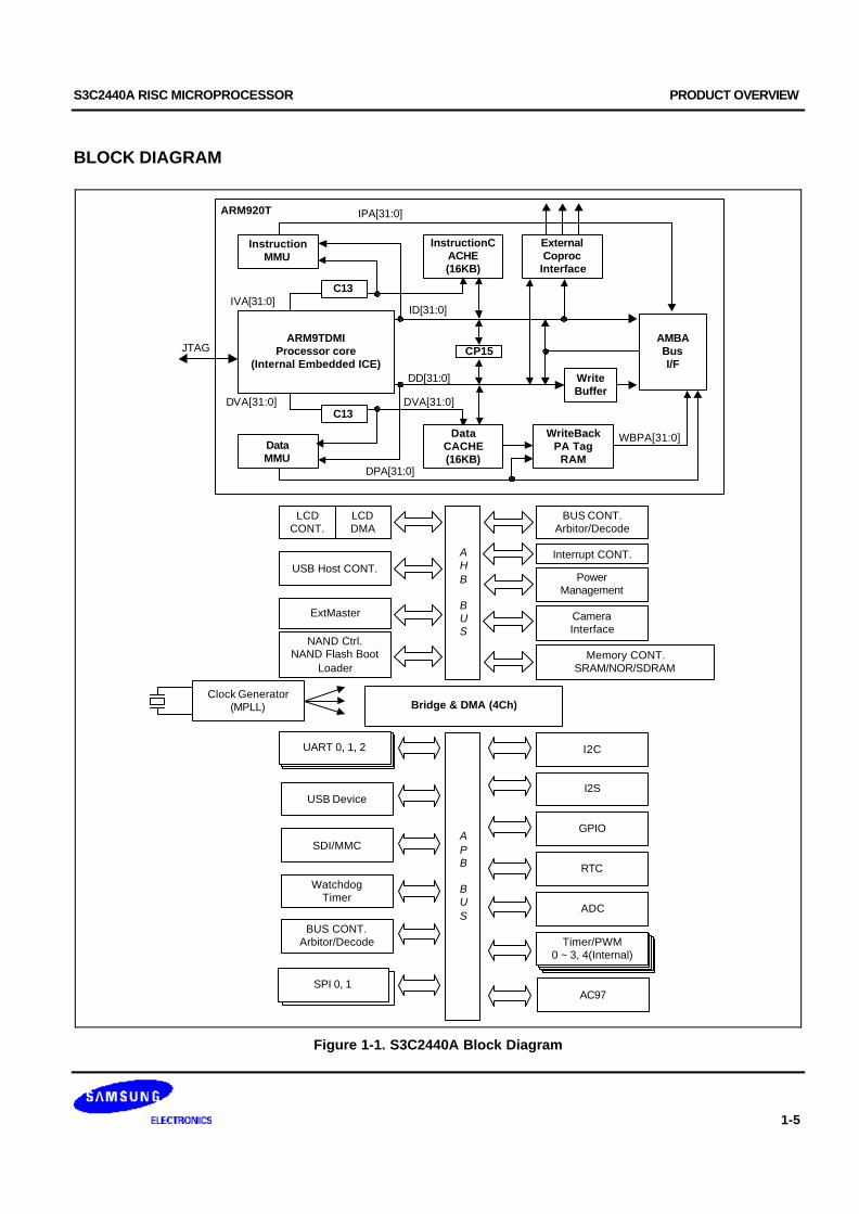
S3C2440A RISC MICROPROCESSOR PRODUCT OVERVIEW
1-5
BLOCK DIAGRAM
ARM920T
ARM9TDMIProcessor core
(Internal Embedded ICE)DD[31:0]
WriteBackPA Tag
RAMDataMMU
C13DVA[31:0]DVA[31:0]
InstructionCACHE(16KB)
InstructionMMU
ExternalCoproc
Interface
C13
ID[31:0]
IPA[31:0]
IVA[31:0]
CP15
WriteBuffer
AMBABusI/F
JTAG
DataCACHE(16KB)
WBPA[31:0]
DPA[31:0]
Bridge & DMA (4Ch)Clock Generator
(MPLL)
AHB
BUS
Memory CONT.SRAM/NOR/SDRAM
BUS CONT.Arbitor/Decode
PowerManagement
Interrupt CONT.USB Host CONT.
ExtMaster
LCDDMA
LCDCONT.
APB
BUS
I2C
GPIO
I2S
RTC
SPI
ADC
SDI/MMC
USB Device
WatchdogTimer
BUS CONT.Arbitor/Decode Timer/PWM
0 ~ 3, 4(Internal)
SPI 0, 1
UART 0, 1, 2
NAND Ctrl.NAND Flash Boot
Loader
CameraInterface
AC97
Figure 1-1. S3C2440A Block Diagram

PRODUCT OVERVIEW S3C2440A RISC MICROPROCESSOR
1-6
PIN ASSIGNMENTS
BOTTOM VIEW
U
T
R
P
N
M
L
K
J
H
G
F
E
D
C
B
A
1 2 3 4 5 6 7 8 9 10 11 12 13 14 15 16 17
Figure 1-2. S3C2440A Pin Assignments (289-FBGA)
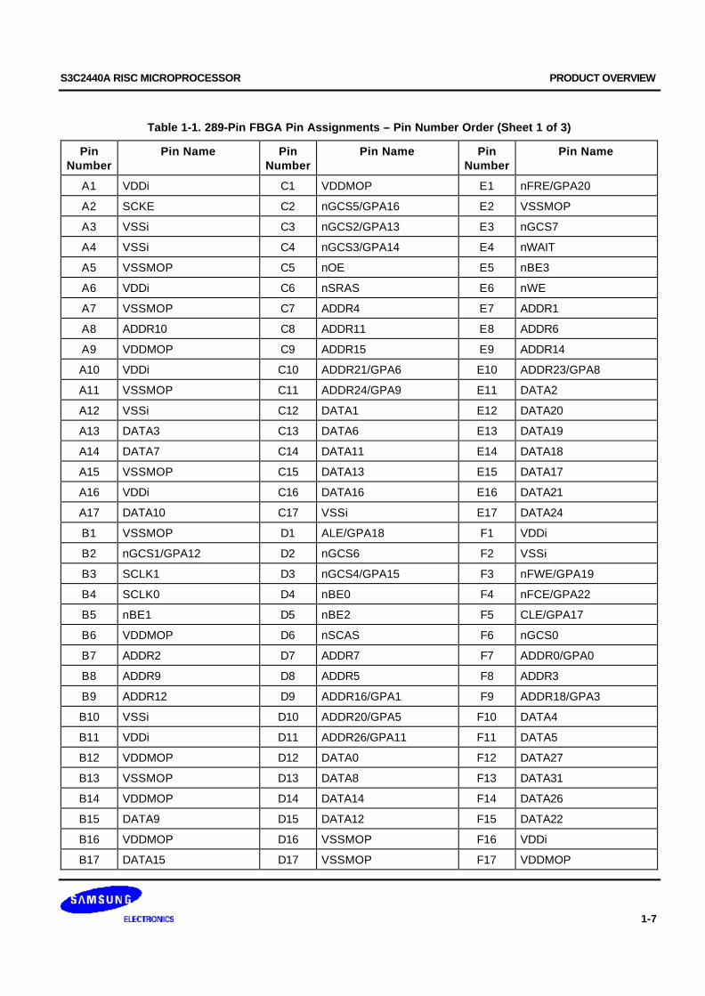
S3C2440A RISC MICROPROCESSOR PRODUCT OVERVIEW
1-7
Table 1-1. 289-Pin FBGA Pin Assignments – Pin Number Order (Sheet 1 of 3)
PinNumber
Pin Name PinNumber
Pin Name PinNumber
Pin Name
A1 VDDi C1 VDDMOP E1 nFRE/GPA20
A2 SCKE C2 nGCS5/GPA16 E2 VSSMOP
A3 VSSi C3 nGCS2/GPA13 E3 nGCS7
A4 VSSi C4 nGCS3/GPA14 E4 nWAIT
A5 VSSMOP C5 nOE E5 nBE3
A6 VDDi C6 nSRAS E6 nWE
A7 VSSMOP C7 ADDR4 E7 ADDR1
A8 ADDR10 C8 ADDR11 E8 ADDR6
A9 VDDMOP C9 ADDR15 E9 ADDR14
A10 VDDi C10 ADDR21/GPA6 E10 ADDR23/GPA8
A11 VSSMOP C11 ADDR24/GPA9 E11 DATA2
A12 VSSi C12 DATA1 E12 DATA20
A13 DATA3 C13 DATA6 E13 DATA19
A14 DATA7 C14 DATA11 E14 DATA18
A15 VSSMOP C15 DATA13 E15 DATA17
A16 VDDi C16 DATA16 E16 DATA21
A17 DATA10 C17 VSSi E17 DATA24
B1 VSSMOP D1 ALE/GPA18 F1 VDDi
B2 nGCS1/GPA12 D2 nGCS6 F2 VSSi
B3 SCLK1 D3 nGCS4/GPA15 F3 nFWE/GPA19
B4 SCLK0 D4 nBE0 F4 nFCE/GPA22
B5 nBE1 D5 nBE2 F5 CLE/GPA17
B6 VDDMOP D6 nSCAS F6 nGCS0
B7 ADDR2 D7 ADDR7 F7 ADDR0/GPA0
B8 ADDR9 D8 ADDR5 F8 ADDR3
B9 ADDR12 D9 ADDR16/GPA1 F9 ADDR18/GPA3
B10 VSSi D10 ADDR20/GPA5 F10 DATA4
B11 VDDi D11 ADDR26/GPA11 F11 DATA5
B12 VDDMOP D12 DATA0 F12 DATA27
B13 VSSMOP D13 DATA8 F13 DATA31
B14 VDDMOP D14 DATA14 F14 DATA26
B15 DATA9 D15 DATA12 F15 DATA22
B16 VDDMOP D16 VSSMOP F16 VDDi
B17 DATA15 D17 VSSMOP F17 VDDMOP
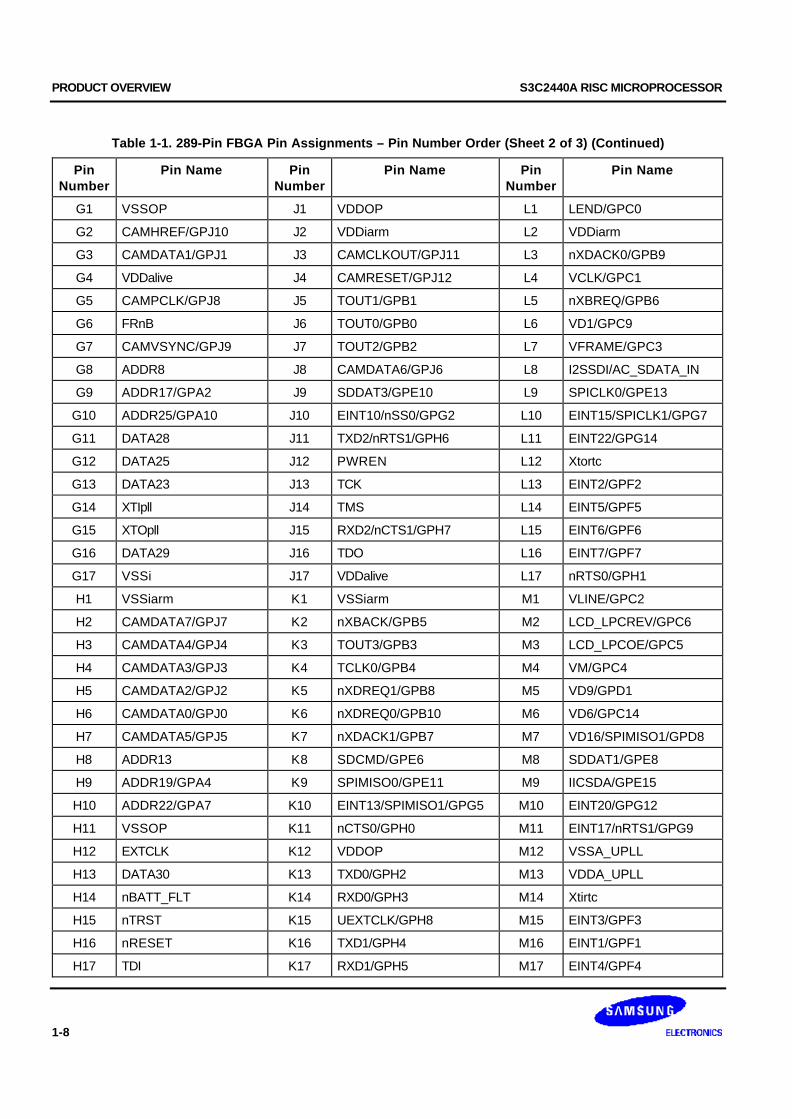
PRODUCT OVERVIEW S3C2440A RISC MICROPROCESSOR
1-8
Table 1-1. 289-Pin FBGA Pin Assignments – Pin Number Order (Sheet 2 of 3) (Continued)
PinNumber
Pin Name PinNumber
Pin Name PinNumber
Pin Name
G1 VSSOP J1 VDDOP L1 LEND/GPC0
G2 CAMHREF/GPJ10 J2 VDDiarm L2 VDDiarm
G3 CAMDATA1/GPJ1 J3 CAMCLKOUT/GPJ11 L3 nXDACK0/GPB9
G4 VDDalive J4 CAMRESET/GPJ12 L4 VCLK/GPC1
G5 CAMPCLK/GPJ8 J5 TOUT1/GPB1 L5 nXBREQ/GPB6
G6 FRnB J6 TOUT0/GPB0 L6 VD1/GPC9
G7 CAMVSYNC/GPJ9 J7 TOUT2/GPB2 L7 VFRAME/GPC3
G8 ADDR8 J8 CAMDATA6/GPJ6 L8 I2SSDI/AC_SDATA_IN
G9 ADDR17/GPA2 J9 SDDAT3/GPE10 L9 SPICLK0/GPE13
G10 ADDR25/GPA10 J10 EINT10/nSS0/GPG2 L10 EINT15/SPICLK1/GPG7
G11 DATA28 J11 TXD2/nRTS1/GPH6 L11 EINT22/GPG14
G12 DATA25 J12 PWREN L12 Xtortc
G13 DATA23 J13 TCK L13 EINT2/GPF2
G14 XTIpll J14 TMS L14 EINT5/GPF5
G15 XTOpll J15 RXD2/nCTS1/GPH7 L15 EINT6/GPF6
G16 DATA29 J16 TDO L16 EINT7/GPF7
G17 VSSi J17 VDDalive L17 nRTS0/GPH1
H1 VSSiarm K1 VSSiarm M1 VLINE/GPC2
H2 CAMDATA7/GPJ7 K2 nXBACK/GPB5 M2 LCD_LPCREV/GPC6
H3 CAMDATA4/GPJ4 K3 TOUT3/GPB3 M3 LCD_LPCOE/GPC5
H4 CAMDATA3/GPJ3 K4 TCLK0/GPB4 M4 VM/GPC4
H5 CAMDATA2/GPJ2 K5 nXDREQ1/GPB8 M5 VD9/GPD1
H6 CAMDATA0/GPJ0 K6 nXDREQ0/GPB10 M6 VD6/GPC14
H7 CAMDATA5/GPJ5 K7 nXDACK1/GPB7 M7 VD16/SPIMISO1/GPD8
H8 ADDR13 K8 SDCMD/GPE6 M8 SDDAT1/GPE8
H9 ADDR19/GPA4 K9 SPIMISO0/GPE11 M9 IICSDA/GPE15
H10 ADDR22/GPA7 K10 EINT13/SPIMISO1/GPG5 M10 EINT20/GPG12
H11 VSSOP K11 nCTS0/GPH0 M11 EINT17/nRTS1/GPG9
H12 EXTCLK K12 VDDOP M12 VSSA_UPLL
H13 DATA30 K13 TXD0/GPH2 M13 VDDA_UPLL
H14 nBATT_FLT K14 RXD0/GPH3 M14 Xtirtc
H15 nTRST K15 UEXTCLK/GPH8 M15 EINT3/GPF3
H16 nRESET K16 TXD1/GPH4 M16 EINT1/GPF1
H17 TDI K17 RXD1/GPH5 M17 EINT4/GPF4

S3C2440A RISC MICROPROCESSOR PRODUCT OVERVIEW
1-9
Table 1-1. 289-Pin FBGA Pin Assignments – Pin Number Order (Sheet 3 of 3) (Continued)
PinNumber
Pin Name PinNumber
Pin Name PinNumber
Pin Name
N1 VSSOP P15 AIN3 T12 VDDOP
N2 VD0/GPC8 P16 XP/AIN7 T13 OM3
N3 VD4/GPC12 P17 UPLLCAP T14 VSSA_ADC
N4 VD2/GPC10 R1 VD3/GPC11 T15 OM0
N5 VD10/GPD2 R2 VD8/GPD0 T16 YM/AIN4
N6 VD15/GPD7 R3 VD11/GPD3 T17 YP/AIN5
N7 VD22/nSS1/GPD14 R4 VD13/GPD5 U1 VDDiarm
N8 SDCLK/GPE5 R5 VD18/SPICLK1/GPD10 U2 VDDiarm
N9 EINT8/GPG0 R6 VD21 /GPD13 U3 VSSOP
N10 EINT18/nCTS1/GPG10 R7 I2SSCLK/AC_BIT_CLK U4 VSSiarm
N11 DP0 R8 SDDAT0/GPE7 U5 VD23/nSS0/GPD15
N12 DN1/PDN0 R9 CLKOUT0/GPH9 U6 I2SSDO/AC_SDATA_OUT
N13 nRSTOUT/GPA21 R10 EINT11/nSS1/GPG3 U7 VSSiarm
N14 MPLLCAP R11 EINT14/SPIMOSI1/GPG6 U8 IICSCL/GPE14
N15 VDD_RTC R12 NCON U9 VSSOP
N16 VDDA_MPLL R13 OM1 U10 VSSiarm
N17 EINT0/GPF0 R14 AIN0 U11 VDDi
P1 LCD_LPCREVB/GPC7 R15 AIN2 U12 EINT19/TCLK1/GPG11
P2 VD5/GPC13 R16 XM/AIN6 U13 EINT23/GPG15
P3 VD7/GPC15 R17 VSSA_MPLL U14 DP1/PDP0
P4 VD12/GPD4 T1 VSSiarm U15 VSSOP
P5 VD14/GPD6 T2 VSSiarm U16 Vref
P6 VD20/GPD12 T3 VDDOP U17 AIN1
P7 I2SLRCK/AC_SYNC T4 VD17/SPIMOSI1/GPD9
P8 SDDAT2/GPE9 T5 VD19/GPD11
P9 SPIMOSI0/GPE12 T6 VDDiarm
P10 CLKOUT1/GPH10 T7 CDCLK/AC_nRESET
P11 EINT12/LCD_PWREN/GPG4
T8 VDDiarm
P12 DN0 T9 EINT9/GPG1
P13 OM2 T10 EINT16/GPG8
P14 VDDA_ADC T11 EINT21/GPG13
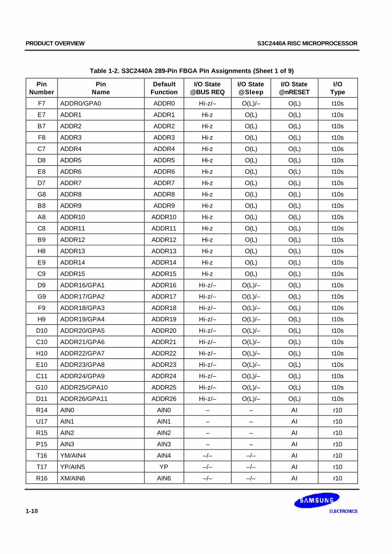
PRODUCT OVERVIEW S3C2440A RISC MICROPROCESSOR
1-10
Table 1-2. S3C2440A 289-Pin FBGA Pin Assignments (Sheet 1 of 9)
PinNumber
PinName
DefaultFunction
I/O State@BUS REQ
I/O State@Sleep
I/O State@nRESET
I/OType
F7 ADDR0/GPA0 ADDR0 Hi-z/– O(L)/– O(L) t10s
E7 ADDR1 ADDR1 Hi-z O(L) O(L) t10s
B7 ADDR2 ADDR2 Hi-z O(L) O(L) t10s
F8 ADDR3 ADDR3 Hi-z O(L) O(L) t10s
C7 ADDR4 ADDR4 Hi-z O(L) O(L) t10s
D8 ADDR5 ADDR5 Hi-z O(L) O(L) t10s
E8 ADDR6 ADDR6 Hi-z O(L) O(L) t10s
D7 ADDR7 ADDR7 Hi-z O(L) O(L) t10s
G8 ADDR8 ADDR8 Hi-z O(L) O(L) t10s
B8 ADDR9 ADDR9 Hi-z O(L) O(L) t10s
A8 ADDR10 ADDR10 Hi-z O(L) O(L) t10s
C8 ADDR11 ADDR11 Hi-z O(L) O(L) t10s
B9 ADDR12 ADDR12 Hi-z O(L) O(L) t10s
H8 ADDR13 ADDR13 Hi-z O(L) O(L) t10s
E9 ADDR14 ADDR14 Hi-z O(L) O(L) t10s
C9 ADDR15 ADDR15 Hi-z O(L) O(L) t10s
D9 ADDR16/GPA1 ADDR16 Hi-z/– O(L)/– O(L) t10s
G9 ADDR17/GPA2 ADDR17 Hi-z/– O(L)/– O(L) t10s
F9 ADDR18/GPA3 ADDR18 Hi-z/– O(L)/– O(L) t10s
H9 ADDR19/GPA4 ADDR19 Hi-z/– O(L)/– O(L) t10s
D10 ADDR20/GPA5 ADDR20 Hi-z/– O(L)/– O(L) t10s
C10 ADDR21/GPA6 ADDR21 Hi-z/– O(L)/– O(L) t10s
H10 ADDR22/GPA7 ADDR22 Hi-z/– O(L)/– O(L) t10s
E10 ADDR23/GPA8 ADDR23 Hi-z/– O(L)/– O(L) t10s
C11 ADDR24/GPA9 ADDR24 Hi-z/– O(L)/– O(L) t10s
G10 ADDR25/GPA10 ADDR25 Hi-z/– O(L)/– O(L) t10s
D11 ADDR26/GPA11 ADDR26 Hi-z/– O(L)/– O(L) t10s
R14 AIN0 AIN0 – – AI r10
U17 AIN1 AIN1 – – AI r10
R15 AIN2 AIN2 – – AI r10
P15 AIN3 AIN3 – – AI r10
T16 YM/AIN4 AIN4 –/– –/– AI r10
T17 YP/AIN5 YP –/– –/– AI r10
R16 XM/AIN6 AIN6 –/– –/– AI r10
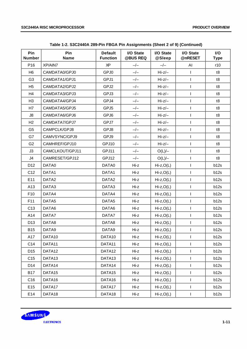
S3C2440A RISC MICROPROCESSOR PRODUCT OVERVIEW
1-11
Table 1-2. S3C2440A 289-Pin FBGA Pin Assignments (Sheet 2 of 9) (Continued)
PinNumber
PinName
DefaultFunction
I/O State@BUS REQ
I/O State@Sleep
I/O State@nRESET
I/OType
P16 XP/AIN7 XP –/– –/– AI r10
H6 CAMDATA0/GPJ0 GPJ0 –/– Hi-z/– I t8
G3 CAMDATA1/GPJ1 GPJ1 –/– Hi-z/– I t8
H5 CAMDATA2/GPJ2 GPJ2 –/– Hi-z/– I t8
H4 CAMDATA3/GPJ3 GPJ3 –/– Hi-z/– I t8
H3 CAMDATA4/GPJ4 GPJ4 –/– Hi-z/– I t8
H7 CAMDATA5/GPJ5 GPJ5 –/– Hi-z/– I t8
J8 CAMDATA6/GPJ6 GPJ6 –/– Hi-z/– I t8
H2 CAMDATA7/GPJ7 GPJ7 –/– Hi-z/– I t8
G5 CAMPCLK/GPJ8 GPJ8 –/– Hi-z/– I t8
G7 CAMVSYNC/GPJ9 GPJ9 –/– Hi-z/– I t8
G2 CAMHREF/GPJ10 GPJ10 –/– Hi-z/– I t8
J3 CAMCLKOUT/GPJ11 GPJ11 –/– O(L)/– I t8
J4 CAMRESET/GPJ12 GPJ12 –/– O(L)/– I t8
D12 DATA0 DATA0 Hi-z Hi-z,O(L) I b12s
C12 DATA1 DATA1 Hi-z Hi-z,O(L) I b12s
E11 DATA2 DATA2 Hi-z Hi-z,O(L) I b12s
A13 DATA3 DATA3 Hi-z Hi-z,O(L) I b12s
F10 DATA4 DATA4 Hi-z Hi-z,O(L) I b12s
F11 DATA5 DATA5 Hi-z Hi-z,O(L) I b12s
C13 DATA6 DATA6 Hi-z Hi-z,O(L) I b12s
A14 DATA7 DATA7 Hi-z Hi-z,O(L) I b12s
D13 DATA8 DATA8 Hi-z Hi-z,O(L) I b12s
B15 DATA9 DATA9 Hi-z Hi-z,O(L) I b12s
A17 DATA10 DATA10 Hi-z Hi-z,O(L) I b12s
C14 DATA11 DATA11 Hi-z Hi-z,O(L) I b12s
D15 DATA12 DATA12 Hi-z Hi-z,O(L) I b12s
C15 DATA13 DATA13 Hi-z Hi-z,O(L) I b12s
D14 DATA14 DATA14 Hi-z Hi-z,O(L) I b12s
B17 DATA15 DATA15 Hi-z Hi-z,O(L) I b12s
C16 DATA16 DATA16 Hi-z Hi-z,O(L) I b12s
E15 DATA17 DATA17 Hi-z Hi-z,O(L) I b12s
E14 DATA18 DATA18 Hi-z Hi-z,O(L) I b12s
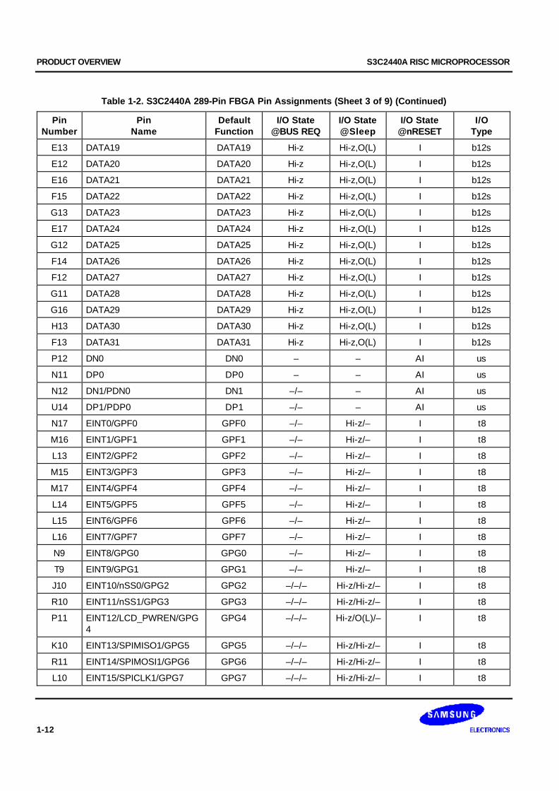
PRODUCT OVERVIEW S3C2440A RISC MICROPROCESSOR
1-12
Table 1-2. S3C2440A 289-Pin FBGA Pin Assignments (Sheet 3 of 9) (Continued)
PinNumber
PinName
DefaultFunction
I/O State@BUS REQ
I/O State@Sleep
I/O State@nRESET
I/OType
E13 DATA19 DATA19 Hi-z Hi-z,O(L) I b12s
E12 DATA20 DATA20 Hi-z Hi-z,O(L) I b12s
E16 DATA21 DATA21 Hi-z Hi-z,O(L) I b12s
F15 DATA22 DATA22 Hi-z Hi-z,O(L) I b12s
G13 DATA23 DATA23 Hi-z Hi-z,O(L) I b12s
E17 DATA24 DATA24 Hi-z Hi-z,O(L) I b12s
G12 DATA25 DATA25 Hi-z Hi-z,O(L) I b12s
F14 DATA26 DATA26 Hi-z Hi-z,O(L) I b12s
F12 DATA27 DATA27 Hi-z Hi-z,O(L) I b12s
G11 DATA28 DATA28 Hi-z Hi-z,O(L) I b12s
G16 DATA29 DATA29 Hi-z Hi-z,O(L) I b12s
H13 DATA30 DATA30 Hi-z Hi-z,O(L) I b12s
F13 DATA31 DATA31 Hi-z Hi-z,O(L) I b12s
P12 DN0 DN0 – – AI us
N11 DP0 DP0 – – AI us
N12 DN1/PDN0 DN1 –/– – AI us
U14 DP1/PDP0 DP1 –/– – AI us
N17 EINT0/GPF0 GPF0 –/– Hi-z/– I t8
M16 EINT1/GPF1 GPF1 –/– Hi-z/– I t8
L13 EINT2/GPF2 GPF2 –/– Hi-z/– I t8
M15 EINT3/GPF3 GPF3 –/– Hi-z/– I t8
M17 EINT4/GPF4 GPF4 –/– Hi-z/– I t8
L14 EINT5/GPF5 GPF5 –/– Hi-z/– I t8
L15 EINT6/GPF6 GPF6 –/– Hi-z/– I t8
L16 EINT7/GPF7 GPF7 –/– Hi-z/– I t8
N9 EINT8/GPG0 GPG0 –/– Hi-z/– I t8
T9 EINT9/GPG1 GPG1 –/– Hi-z/– I t8
J10 EINT10/nSS0/GPG2 GPG2 –/–/– Hi-z/Hi-z/– I t8
R10 EINT11/nSS1/GPG3 GPG3 –/–/– Hi-z/Hi-z/– I t8
P11 EINT12/LCD_PWREN/GPG4
GPG4 –/–/– Hi-z/O(L)/– I t8
K10 EINT13/SPIMISO1/GPG5 GPG5 –/–/– Hi-z/Hi-z/– I t8
R11 EINT14/SPIMOSI1/GPG6 GPG6 –/–/– Hi-z/Hi-z/– I t8
L10 EINT15/SPICLK1/GPG7 GPG7 –/–/– Hi-z/Hi-z/– I t8

S3C2440A RISC MICROPROCESSOR PRODUCT OVERVIEW
1-13
Table 1-2. S3C2440A 289-Pin FBGA Pin Assignments (Sheet 4 of 9) (Continued)
PinNumber
PinName
DefaultFunction
I/O State@BUS REQ
I/O State@Sleep
I/O State@nRESET
I/OType
T10 EINT16/GPG8 GPG8 –/– Hi-z/– I t8
M11 EINT17/nRTS1/GPG9 GPG9 –/–/– Hi-z/O(H)/– I t8
N10 EINT18/nCTS1/GPG10 GPG10 –/–/– Hi-z/Hi-z/– I t8
U12 EINT19/TCLK1/GPG11 GPG11 –/–/– Hi-z/Hi-z/– I t12
M10 EINT20/GPG12 GPG12 –/– Hi-z/– I t12
T11 EINT21/GPG13 GPG13 –/– Hi-z/– I t12
L11 EINT22/GPG14 GPG14 –/– Hi-z/– I t12
U13 EINT23/GPG15 GPG15 –/– Hi-z/– I t12
H12 EXTCLK EXTCLK – – AI is
P17 UPLLCAP UPLLCAP – – AI r50
N14 MPLLCAP MPLLCAP – – AI r50
H14 nBATT_FLT nBATT_FLT – – I is
D4 nBE0 nBE0 Hi-z Hi-z,O(H) O(H) t10s
B5 nBE1 nBE1 Hi-z Hi-z,O(H) O(H) t10s
D5 nBE2 nBE2 Hi-z Hi-z,O(H) O(H) t10s
E5 nBE3 nBE3 Hi-z Hi-z,O(H) O(H) t10s
R12 NCON NCON – – I is
G6 FRnB FRnB – Hi-z,O(L) I d2s
F3 nFWE/GPA19 GPA19 O(H)/– Hi-z,O(H)/– O(H) t10s
E1 nFRE/GPA20 GPA20 O(H)/– Hi-z,O(H)/– O(H) t10s
F4 nFCE/GPA22 GPA21 O(H)/– Hi-z,O(H)/– O(H) t10s
F5 CLE/GPA17 GPA17 O(L)/– Hi-z,O(L)/– O(L) t10s
D1 ALE/GPA18 GPA18 O(L)/– Hi-z,O(L)/– O(L) t10s
N13 nRSTOUT/GPA21 GPA21 –/– O(L)/– O(L) b8
C5 nOE nOE Hi-z Hi-z,O(H) O(H) t10s
H16 nRESET nRESET – – I is
F6 nGCS0 nGCS0 Hi-z Hi-z,O(H) O(H) t10s
B2 nGCS1/GPA12 GPA12 Hi-z/– Hi-z,O(H)/– O(H) t10s
C3 nGCS2/GPA13 GPA13 Hi-z/– Hi-z,O(H)/– O(H) t10s
C4 nGCS3/GPA14 GPA14 Hi-z/– Hi-z,O(H)/– O(H) t10s
D3 nGCS4/GPA15 GPA15 Hi-z/– Hi-z,O(H)/– O(H) t10s
C2 nGCS5/GPA16 GPA16 Hi-z/– Hi-z,O(H)/– O(H) t10s
D2 nGCS6 nGCS6 Hi-z Hi-z,O(H) O(H) t10s

PRODUCT OVERVIEW S3C2440A RISC MICROPROCESSOR
1-14
Table 1-2. S3C2440A 289-Pin FBGA Pin Assignments (Sheet 5 of 9) (Continued)
PinNumber
PinName
DefaultFunction
I/O State@BUS REQ
I/O State@Sleep
I/O State@nRESET
I/OType
E3 nGCS7 nGCS7 Hi-z Hi-z,O(H) O(H) t10s
D6 nSCAS nSCAS Hi-z Hi-z,O(H) O(H) t10s
C6 nSRAS nSRAS Hi-z Hi-z,O(H) O(H) t10s
H15 nTRST nTRST I – I is
E4 nWAIT nWAIT – Hi-z,O(L) I d2s
E6 nWE nWE Hi-z Hi-z,O(H) O(H) t10s
J6 TOUT0/GPB0 GPB0 –/– O(L)/– I t8
J5 TOUT1/GPB1 GPB1 –/– O(L)/– I t8
J7 TOUT2/GPB2 GPB2 –/– O(L)/– I t8
K3 TOUT3/GPB3 GPB3 –/– O(L)/– I t8
K4 TCLK0/GPB4 GPB4 –/– –/– I t8
K2 nXBACK/GPB5 GPB5 –/– O(H)/– I t8
L5 nXBREQ/GPB6 GPB6 –/– –/– I t8
K7 nXDACK1/GPB7 GPB7 –/– O(H)/– I t8
K5 nXDREQ1/GPB8 GPB8 –/– –/– I t8
L3 nXDACK0/GPB9 GPB9 –/– O(H)/– I t8
K6 nXDREQ0/GPB10 GPB10 –/– –/– I t8
T15 OM0 OM0 – – I is
R13 OM1 OM1 – – I is
P13 OM2 OM2 – – I is
T13 OM3 OM3 – – I is
J12 PWREN PWREN O(H) O(L) O(H) b8
K11 nCTS0/GPH0 GPH0 –/– –/– I t8
L17 nRTS0/GPH1 GPH1 –/– O(H)/– I t8
K13 TXD0/GPH2 GPH2 –/– O(H)/– I t8
K14 RXD0/GPH3 GPH3 –/– –/– I t8
K16 TXD1/GPH4 GPH4 –/– O(H)/– I t8
K17 RXD1/GPH5 GPH5 –/– –/– I t8
J11 TXD2/nRTS1/GPH6 GPH6 –/–/– O(H)/O(H)/– I t8
J15 RXD2/nCTS1/GPH7 GPH7 –/–/– Hi-z/Hi-z/– I t8
K15 UEXTCLK/GPH8 GPH8 –/– Hi-z/– I t8
R9 CLKOUT0/GPH9 GPH9 –/– O(L)/– I t12
P10 CLKOUT1/GPH10 GPH10 –/– O(L)/– I t12
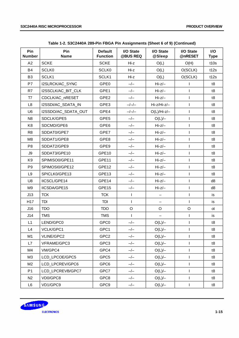
S3C2440A RISC MICROPROCESSOR PRODUCT OVERVIEW
1-15
Table 1-2. S3C2440A 289-Pin FBGA Pin Assignments (Sheet 6 of 9) (Continued)
PinNumber
PinName
DefaultFunction
I/O State@BUS REQ
I/O State@Sleep
I/O State@nRESET
I/OType
A2 SCKE SCKE Hi-z O(L) O(H) t10s
B4 SCLK0 SCLK0 Hi-z O(L) O(SCLK) t12s
B3 SCLK1 SCLK1 Hi-z O(L) O(SCLK) t12s
P7 I2SLRCK/AC_SYNC GPE0 –/– Hi-z/– I t8
R7 I2SSCLK/AC_BIT_CLK GPE1 –/– Hi-z/– I t8
T7 CDCLK/AC_nRESET GPE2 –/– Hi-z/– I t8
L8 I2SSDI/AC_SDATA_IN GPE3 –/–/– Hi-z/Hi-z/– I t8
U6 I2SSDO/AC_SDATA_OUT GPE4 –/–/– O(L)/Hi-z/– I t8
N8 SDCLK/GPE5 GPE5 –/– O(L)/– I t8
K8 SDCMD/GPE6 GPE6 –/– Hi-z/– I t8
R8 SDDAT0/GPE7 GPE7 –/– Hi-z/– I t8
M8 SDDAT1/GPE8 GPE8 –/– Hi-z/– I t8
P8 SDDAT2/GPE9 GPE9 –/– Hi-z/– I t8
J9 SDDAT3/GPE10 GPE10 –/– Hi-z/– I t8
K9 SPIMISO0/GPE11 GPE11 –/– Hi-z/– I t8
P9 SPIMOSI0/GPE12 GPE12 –/– Hi-z/– I t8
L9 SPICLK0/GPE13 GPE13 –/– Hi-z/– I t8
U8 IICSCL/GPE14 GPE14 –/– Hi-z/– I d8
M9 IICSDA/GPE15 GPE15 –/– Hi-z/– I d8
J13 TCK TCK I – I is
H17 TDI TDI I – I is
J16 TDO TDO O O O ot
J14 TMS TMS I – I is
L1 LEND/GPC0 GPC0 –/– O(L)/– I t8
L4 VCLK/GPC1 GPC1 –/– O(L)/– I t8
M1 VLINE/GPC2 GPC2 –/– O(L)/– I t8
L7 VFRAME/GPC3 GPC3 –/– O(L)/– I t8
M4 VM/GPC4 GPC4 –/– O(L)/– I t8
M3 LCD_LPCOE/GPC5 GPC5 –/– O(L)/– I t8
M2 LCD_LPCREV/GPC6 GPC6 –/– O(L)/– I t8
P1 LCD_LPCREVB/GPC7 GPC7 –/– O(L)/– I t8
N2 VD0/GPC8 GPC8 –/– O(L)/– I t8
L6 VD1/GPC9 GPC9 –/– O(L)/– I t8
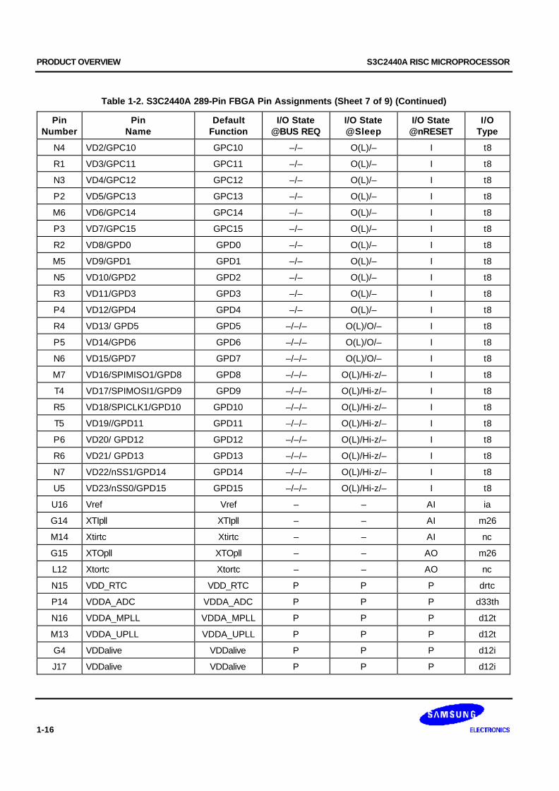
PRODUCT OVERVIEW S3C2440A RISC MICROPROCESSOR
1-16
Table 1-2. S3C2440A 289-Pin FBGA Pin Assignments (Sheet 7 of 9) (Continued)
PinNumber
PinName
DefaultFunction
I/O State@BUS REQ
I/O State@Sleep
I/O State@nRESET
I/OType
N4 VD2/GPC10 GPC10 –/– O(L)/– I t8
R1 VD3/GPC11 GPC11 –/– O(L)/– I t8
N3 VD4/GPC12 GPC12 –/– O(L)/– I t8
P2 VD5/GPC13 GPC13 –/– O(L)/– I t8
M6 VD6/GPC14 GPC14 –/– O(L)/– I t8
P3 VD7/GPC15 GPC15 –/– O(L)/– I t8
R2 VD8/GPD0 GPD0 –/– O(L)/– I t8
M5 VD9/GPD1 GPD1 –/– O(L)/– I t8
N5 VD10/GPD2 GPD2 –/– O(L)/– I t8
R3 VD11/GPD3 GPD3 –/– O(L)/– I t8
P4 VD12/GPD4 GPD4 –/– O(L)/– I t8
R4 VD13/ GPD5 GPD5 –/–/– O(L)/O/– I t8
P5 VD14/GPD6 GPD6 –/–/– O(L)/O/– I t8
N6 VD15/GPD7 GPD7 –/–/– O(L)/O/– I t8
M7 VD16/SPIMISO1/GPD8 GPD8 –/–/– O(L)/Hi-z/– I t8
T4 VD17/SPIMOSI1/GPD9 GPD9 –/–/– O(L)/Hi-z/– I t8
R5 VD18/SPICLK1/GPD10 GPD10 –/–/– O(L)/Hi-z/– I t8
T5 VD19//GPD11 GPD11 –/–/– O(L)/Hi-z/– I t8
P6 VD20/ GPD12 GPD12 –/–/– O(L)/Hi-z/– I t8
R6 VD21/ GPD13 GPD13 –/–/– O(L)/Hi-z/– I t8
N7 VD22/nSS1/GPD14 GPD14 –/–/– O(L)/Hi-z/– I t8
U5 VD23/nSS0/GPD15 GPD15 –/–/– O(L)/Hi-z/– I t8
U16 Vref Vref – – AI ia
G14 XTIpll XTIpll – – AI m26
M14 Xtirtc Xtirtc – – AI nc
G15 XTOpll XTOpll – – AO m26
L12 Xtortc Xtortc – – AO nc
N15 VDD_RTC VDD_RTC P P P drtc
P14 VDDA_ADC VDDA_ADC P P P d33th
N16 VDDA_MPLL VDDA_MPLL P P P d12t
M13 VDDA_UPLL VDDA_UPLL P P P d12t
G4 VDDalive VDDalive P P P d12i
J17 VDDalive VDDalive P P P d12i
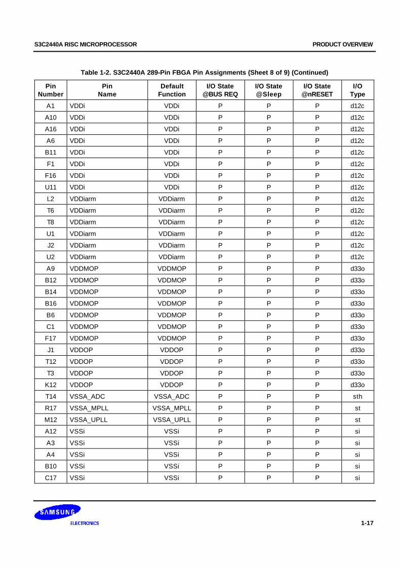
S3C2440A RISC MICROPROCESSOR PRODUCT OVERVIEW
1-17
Table 1-2. S3C2440A 289-Pin FBGA Pin Assignments (Sheet 8 of 9) (Continued)
PinNumber
PinName
DefaultFunction
I/O State@BUS REQ
I/O State@Sleep
I/O State@nRESET
I/OType
A1 VDDi VDDi P P P d12c
A10 VDDi VDDi P P P d12c
A16 VDDi VDDi P P P d12c
A6 VDDi VDDi P P P d12c
B11 VDDi VDDi P P P d12c
F1 VDDi VDDi P P P d12c
F16 VDDi VDDi P P P d12c
U11 VDDi VDDi P P P d12c
L2 VDDiarm VDDiarm P P P d12c
T6 VDDiarm VDDiarm P P P d12c
T8 VDDiarm VDDiarm P P P d12c
U1 VDDiarm VDDiarm P P P d12c
J2 VDDiarm VDDiarm P P P d12c
U2 VDDiarm VDDiarm P P P d12c
A9 VDDMOP VDDMOP P P P d33o
B12 VDDMOP VDDMOP P P P d33o
B14 VDDMOP VDDMOP P P P d33o
B16 VDDMOP VDDMOP P P P d33o
B6 VDDMOP VDDMOP P P P d33o
C1 VDDMOP VDDMOP P P P d33o
F17 VDDMOP VDDMOP P P P d33o
J1 VDDOP VDDOP P P P d33o
T12 VDDOP VDDOP P P P d33o
T3 VDDOP VDDOP P P P d33o
K12 VDDOP VDDOP P P P d33o
T14 VSSA_ADC VSSA_ADC P P P sth
R17 VSSA_MPLL VSSA_MPLL P P P st
M12 VSSA_UPLL VSSA_UPLL P P P st
A12 VSSi VSSi P P P si
A3 VSSi VSSi P P P si
A4 VSSi VSSi P P P si
B10 VSSi VSSi P P P si
C17 VSSi VSSi P P P si

PRODUCT OVERVIEW S3C2440A RISC MICROPROCESSOR
1-18
Table 1-2. S3C2440A 289-Pin FBGA Pin Assignments (Sheet 9 of 9) (Continued)
PinNumber
PinName
DefaultFunction
I/O State@BUS REQ
I/O State@Sleep
I/O State@nRESET
I/OType
F2 VSSi VSSi P P P si
G17 VSSi VSSi P P P si
H1 VSSiarm VSSiarm P P P si
K1 VSSiarm VSSiarm P P P si
T1 VSSiarm VSSiarm P P P si
T2 VSSiarm VSSiarm P P P si
U10 VSSiarm VSSiarm P P P si
U4 VSSiarm VSSiarm P P P si
U7 VSSiarm VSSiarm P P P si
A11 VSSMOP VSSMOP P P P so
A15 VSSMOP VSSMOP P P P so
A5 VSSMOP VSSMOP P P P so
A7 VSSMOP VSSMOP P P P so
B1 VSSMOP VSSMOP P P P so
B13 VSSMOP VSSMOP P P P so
D16 VSSMOP VSSMOP P P P so
D17 VSSMOP VSSMOP P P P so
E2 VSSMOP VSSMOP P P P so
G1 VSSOP VSSOP P P P so
N1 VSSOP VSSOP P P P so
U15 VSSOP VSSOP P P P so
U3 VSSOP VSSOP P P P so
U9 VSSOP VSSOP P P P so
H11 VSSOP VSSOP P P P so
NOTES:1. The @BUS REQ. shows the pin state at the external bus, which is used by the other bus master.2. ' – ‘ mark indicates the unchanged pin state at Bus Request mode.3. Hi-z or Pre means Hi-z or early state and it is determined by the setting of MISCCR register.4. AI/AO means analog input/analog output.5. P, I, and O mean power, input and output respectively.6. The I/O state @nRESET shows the pin status in the @nRESET duration below.
nRESET
FCLK
@nRESET4 OSCin
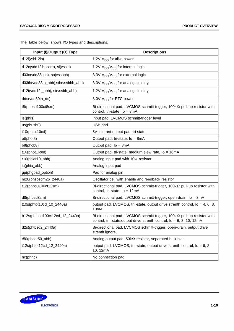
S3C2440A RISC MICROPROCESSOR PRODUCT OVERVIEW
1-19
The table below shows I/O types and descriptions.
Input (I)/Output (O) Type Descriptions
d12i(vdd12ih) 1.2V VDD for alive power
d12c(vdd12ih_core), si(vssih) 1.2V VDD/VSS for internal logic
d33o(vdd33oph), so(vssoph) 3.3V VDD/VSS for external logic
d33th(vdd33th_abb),sth(vssbbh_abb) 3.3V VDD/VSS for analog circuitry
d12t(vdd12t_abb), st(vssbb_abb) 1.2V VDD/VSS for analog circuitry
drtc(vdd30th_rtc) 3.0V VDD for RTC power
t8(phbsu100ct8sm) Bi-directional pad, LVCMOS schmitt-trigger, 100kΩ pull-up resistor withcontrol, tri-state, Io = 8mA
is(phis) Input pad, LVCMOS schmitt-trigger level
us(pbusb0) USB pad
t10(phtot10cd) 5V tolerant output pad, tri-state.
ot(phot8) Output pad, tri-state, Io = 8mA
b8(phob8) Output pad, Io = 8mA
t16(phot16sm) Output pad, tri-state, medium slew rate, Io = 16mA
r10(phiar10_abb) Analog input pad with 10Ω resistor
ia(phia_abb) Analog input pad
gp(phgpad_option) Pad for analog pin
m26(phsoscm26_2440a) Oscillator cell with enable and feedback resistor
t12(phbsu100ct12sm) Bi-directional pad, LVCMOS schmitt-trigger, 100kΩ pull-up resistor withcontrol, tri-state, Io = 12mA
d8(phbsd8sm) Bi-directional pad, LVCMOS schmitt-trigger, open drain, Io = 8mA
t10s(phtot10cd_10_2440a) output pad, LVCMOS, tri -state, output drive strenth control, Io = 4, 6, 8,10mA
b12s(phtbsu100ct12cd_12_2440a) Bi-directional pad, LVCMOS schmitt-trigger, 100kΩ pull-up resistor withcontrol, tri -state,output drive strenth control, Io = 6, 8, 10, 12mA
d2s(phtbsd2_2440a) Bi-directional pad, LVCMOS schmitt-trigger, open-drain, output drivestrenth ignore,
r50(phoar50_abb) Analog output pad, 50kΩ resistor, separated bulk-bias
t12s(phtot12cd_12_2440a) output pad, LVCMOS, tri -state, output drive strenth control, Io = 6, 8,10, 12mA
nc(phnc) No connection pad

PRODUCT OVERVIEW S3C2440A RISC MICROPROCESSOR
1-20
SIGNAL DESCRIPTIONS
Table 1-3. S3C2440A Signal Descriptions (Sheet 1 of 6)
Signal Input/Output DescriptionsBus ControllerOM[1:0] I OM[1:0] sets S3C2440A in the TEST mode, which is used only at fabrication.
Also, it determines the bus width of nGCS0. The pull-up/down resistordetermines the logic level during RESET cycle.00: Nand-boot 01: 16-bit 10: 32-bit 11: Test mode
ADDR[26:0] O ADDR[26:0] (Address Bus) outputs the memory address of the correspondingbank .
DATA[31:0] IO DATA[31:0] (Data Bus) inputs data during memory read and outputs data duringmemory write. The bus width is programmable among 8/16/32-bit.
nGCS[7:0] O nGCS[7:0] (General Chip Select) are activated when the address of a memory iswithin the address region of each bank. The number of access cycles and thebank size can be programmed.
nWE O nWE (Write Enable) indicates that the current bus cycle is a write cycle.nOE O nOE (Output Enable) indicates that the current bus cycle is a read cycle.nXBREQ I nXBREQ (Bus Hold Request) allows another bus master to request control of the
local bus. BACK active indicates that bus control has been granted.nXBACK O nXBACK (Bus Hold Acknowledge) indicates that the S3C2440A has surrendered
control of the local bus to another bus master.nWAIT I nWAIT requests to prolong a current bus cycle. As long as nWAIT is L, the
current bus cycle cannot be completed.SDRAM/SRAMnSRAS O SDRAM row address strobenSCAS O SDRAM column address strobenSCS[1:0] O SDRAM chip selectDQM[3:0] O SDRAM data maskSCLK[1:0] O SDRAM clockSCKE O SDRAM clock enablenBE[3:0] O Upper byte/lower byte enable (In case of 16-bit SRAM)nWBE[3:0] O Write byte enableNAND FlashCLE O Command latch enableALE O Address latch enablenFCE O Nand flash chip enablenFRE O Nand flash read enablenFWE O Nand flash write enableNCON I Nand flash configuration * If NAND flash controller isn’t used, it
has to be pull-up. (VDDMOP)FRnB I Nand flash ready/busy

S3C2440A RISC MICROPROCESSOR PRODUCT OVERVIEW
1-21
Table 1-3. S3C2440A Signal Descriptions (Sheet 2 of 6) (Continued)
Signal Input/Output
Descriptions
LCD Control Unit
VD[23:0] O STN/TFT/SEC TFT: LCD data bus
LCD_PWREN O STN/TFT/SEC TFT: LCD panel power enable control signal
VCLK O STN/TFT: LCD clock signal
VFRAME O STN: LCD frame signal
VLINE O STN: LCD line signal
VM O STN: VM alternates the polarity of the row and column voltage
VSYNC O TFT: Vertical synchronous signal
HSYNC O TFT: Horizontal synchronous signal
VDEN O TFT: Data enable signal
LEND O TFT: Line end signal
STV O SEC TFT: SEC(Samsung Electronics Company) TFT LCD panel control signal
CPV O SEC TFT: SEC(Samsung Electronics Company) TFT LCD panel control signal
LCD_HCLK O SEC TFT: SEC(Samsung Electronics Company) TFT LCD panel control signal
TP O SEC TFT: SEC(Samsung Electronics Company) TFT LCD panel control signal
STH O SEC TFT: SEC(Samsung Electronics Company) TFT LCD panel control signal
LCD_LPCOE O SEC TFT: Timing control signal for specific TFT LCD
LCD_LPCREV O SEC TFT: Timing control signal for specific TFT LCD
LCD_LPCREVB O SEC TFT: Timing control signal for specific TFT LCD
CAMERA Interface
CAMRESET O Software reset to the camera
CAMCLKOUT O Master clock to the camera
CAMPCLK I Pixel clock from camera
CAMHREF I Horizontal sync signal from camera
CAMVSYNC I Vertical sync signal from camera
CAMDATA[7:0] I Pixel data for YCbCr
Interrupt Control Unit
EINT[23:0] I External interrupt request
DMA
nXDREQ[1:0] I External DMA request
nXDACK[1:0] O External DMA acknowledge
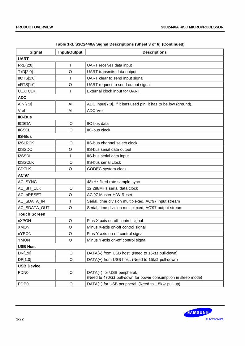
PRODUCT OVERVIEW S3C2440A RISC MICROPROCESSOR
1-22
Table 1-3. S3C2440A Signal Descriptions (Sheet 3 of 6) (Continued)
Signal Input/Output Descriptions
UART
RxD[2:0] I UART receives data input
TxD[2:0] O UART transmits data output
nCTS[1:0] I UART clear to send input signal
nRTS[1:0] O UART request to send output signal
UEXTCLK I External clock input for UART
ADC
AIN[7:0] AI ADC input[7:0]. If it isn’t used pin, it has to be low (ground).
Vref AI ADC Vref
IIC-Bus
IICSDA IO IIC-bus data
IICSCL IO IIC-bus clock
IIS-Bus
I2SLRCK IO IIS-bus channel select clock
I2SSDO O IIS-bus serial data output
I2SSDI I IIS-bus serial data input
I2SSCLK IO IIS-bus serial clock
CDCLK O CODEC system clock
AC’97
AC_SYNC 48kHz fixed rate sample sync
AC_BIT_CLK IO 12.288MHz serial data clock
AC_nRESET O AC’97 Master H/W Reset
AC_SDATA_IN I Serial, time division multiplexed, AC’97 input stream
AC_SDATA_OUT O Serial, time division multiplexed, AC’97 output stream
Touch Screen
nXPON O Plus X-axis on-off control signal
XMON O Minus X-axis on-off control signal
nYPON O Plus Y-axis on-off control signal
YMON O Minus Y-axis on-off control signal
USB Host
DN[1:0] IO DATA(–) from USB host. (Need to 15kΩ pull-down)
DP[1:0] IO DATA(+) from USB host. (Need to 15kΩ pull-down)
USB Device
PDN0 IO DATA(–) for USB peripheral.(Need to 470kΩ pull-down for power consumption in sleep mode)
PDP0 IO DATA(+) for USB peripheral. (Need to 1.5kΩ pull-up)
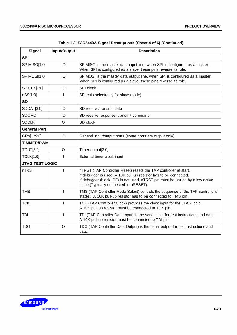
S3C2440A RISC MICROPROCESSOR PRODUCT OVERVIEW
1-23
Table 1-3. S3C2440A Signal Descriptions (Sheet 4 of 6) (Continued)
Signal Input/Output Description
SPI
SPIMISO[1:0] IO SPIMISO is the master data input line, when SPI is configured as a master.When SPI is configured as a slave, these pins reverse its role.
SPIMOSI[1:0] IO SPIMOSI is the master data output line, when SPI is configured as a master.When SPI is configured as a slave, these pins reverse its role.
SPICLK[1:0] IO SPI clock
nSS[1:0] I SPI chip select(only for slave mode)
SD
SDDAT[3:0] IO SD receive/transmit data
SDCMD IO SD receive response/ transmit command
SDCLK O SD clock
General Port
GPn[129:0] IO General input/output ports (some ports are output only)
TIMMER/PWM
TOUT[3:0] O Timer output[3:0]
TCLK[1:0] I External timer clock input
JTAG TEST LOGIC
nTRST I nTRST (TAP Controller Reset) resets the TAP controller at start.If debugger is used, A 10K pull-up resistor has to be connected.If debugger (black ICE) is not used, nTRST pin must be issued by a low activepulse (Typically connected to nRESET).
TMS I TMS (TAP Controller Mode Select) controls the sequence of the TAP controller'sstates. A 10K pull-up resistor has to be connected to TMS pin.
TCK I TCK (TAP Controller Clock) provides the clock input for the JTAG logic.A 10K pull-up resistor must be connected to TCK pin.
TDI I TDI (TAP Controller Data Input) is the serial input for test instructions and data.A 10K pull-up resistor must be connected to TDI pin.
TDO O TDO (TAP Controller Data Output) is the serial output for test instructions anddata.
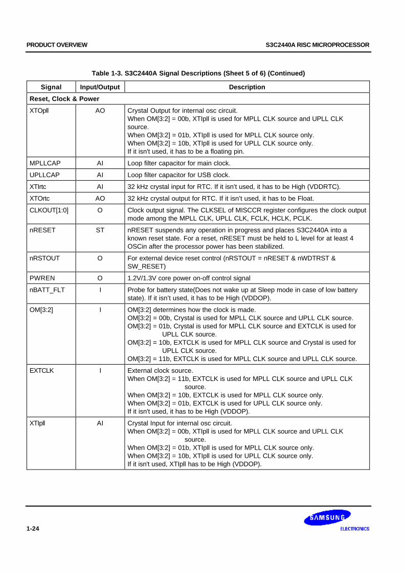
PRODUCT OVERVIEW S3C2440A RISC MICROPROCESSOR
1-24
Table 1-3. S3C2440A Signal Descriptions (Sheet 5 of 6) (Continued)
Signal Input/Output Description
Reset, Clock & Power
XTOpll AO Crystal Output for internal osc circuit.When OM[3:2] = 00b, XTIpll is used for MPLL CLK source and UPLL CLKsource.When OM[3:2] = 01b, XTIpll is used for MPLL CLK source only.When OM[3:2] = 10b, XTIpll is used for UPLL CLK source only.If it isn't used, it has to be a floating pin.
MPLLCAP AI Loop filter capacitor for main clock.
UPLLCAP AI Loop filter capacitor for USB clock.
XTIrtc AI 32 kHz crystal input for RTC. If it isn’t used, it has to be High (VDDRTC).
XTOrtc AO 32 kHz crystal output for RTC. If it isn’t used, it has to be Float.
CLKOUT[1:0] O Clock output signal. The CLKSEL of MISCCR register configures the clock outputmode among the MPLL CLK, UPLL CLK, FCLK, HCLK, PCLK.
nRESET ST nRESET suspends any operation in progress and places S3C2440A into aknown reset state. For a reset, nRESET must be held to L level for at least 4OSCin after the processor power has been stabilized.
nRSTOUT O For external device reset control (nRSTOUT = nRESET & nWDTRST &SW_RESET)
PWREN O 1.2V/1.3V core power on-off control signal
nBATT_FLT I Probe for battery state(Does not wake up at Sleep mode in case of low batterystate). If it isn’t used, it has to be High (VDDOP).
OM[3:2] I OM[3:2] determines how the clock is made.OM[3:2] = 00b, Crystal is used for MPLL CLK source and UPLL CLK source.OM[3:2] = 01b, Crystal is used for MPLL CLK source and EXTCLK is used for UPLL CLK source.OM[3:2] = 10b, EXTCLK is used for MPLL CLK source and Crystal is used for UPLL CLK source.OM[3:2] = 11b, EXTCLK is used for MPLL CLK source and UPLL CLK source.
EXTCLK I External clock source.When OM[3:2] = 11b, EXTCLK is used for MPLL CLK source and UPLL CLK source.When OM[3:2] = 10b, EXTCLK is used for MPLL CLK source only.When OM[3:2] = 01b, EXTCLK is used for UPLL CLK source only.If it isn't used, it has to be High (VDDOP).
XTIpll AI Crystal Input for internal osc circuit.When OM[3:2] = 00b, XTIpll is used for MPLL CLK source and UPLL CLK source.When OM[3:2] = 01b, XTIpll is used for MPLL CLK source only.When OM[3:2] = 10b, XTIpll is used for UPLL CLK source only.If it isn't used, XTIpll has to be High (VDDOP).
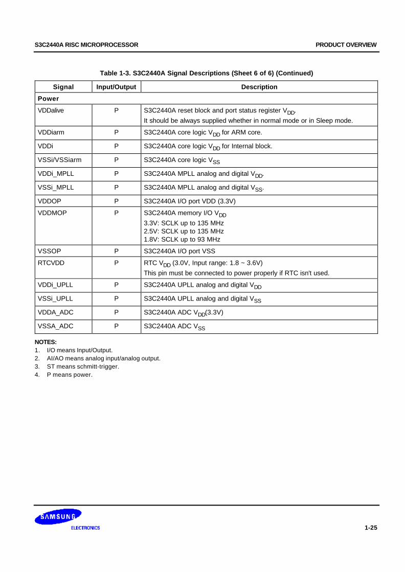
S3C2440A RISC MICROPROCESSOR PRODUCT OVERVIEW
1-25
Table 1-3. S3C2440A Signal Descriptions (Sheet 6 of 6) (Continued)
Signal Input/Output Description
Power
VDDalive P S3C2440A reset block and port status register VDD.
It should be always supplied whether in normal mode or in Sleep mode.
VDDiarm P S3C2440A core logic VDD for ARM core.
VDDi P S3C2440A core logic VDD for Internal block.
VSSi/VSSiarm P S3C2440A core logic VSS
VDDi_MPLL P S3C2440A MPLL analog and digital VDD.
VSSi_MPLL P S3C2440A MPLL analog and digital VSS.
VDDOP P S3C2440A I/O port VDD (3.3V)
VDDMOP P S3C2440A memory I/O VDD3.3V: SCLK up to 135 MHz2.5V: SCLK up to 135 MHz1.8V: SCLK up to 93 MHz
VSSOP P S3C2440A I/O port VSS
RTCVDD P RTC VDD (3.0V, Input range: 1.8 ~ 3.6V)
This pin must be connected to power properly if RTC isn't used.
VDDi_UPLL P S3C2440A UPLL analog and digital VDD
VSSi_UPLL P S3C2440A UPLL analog and digital VSS
VDDA_ADC P S3C2440A ADC VDD(3.3V)
VSSA_ADC P S3C2440A ADC VSS
NOTES:1. I/O means Input/Output.2. AI/AO means analog input/analog output.3. ST means schmitt-trigger.4. P means power.
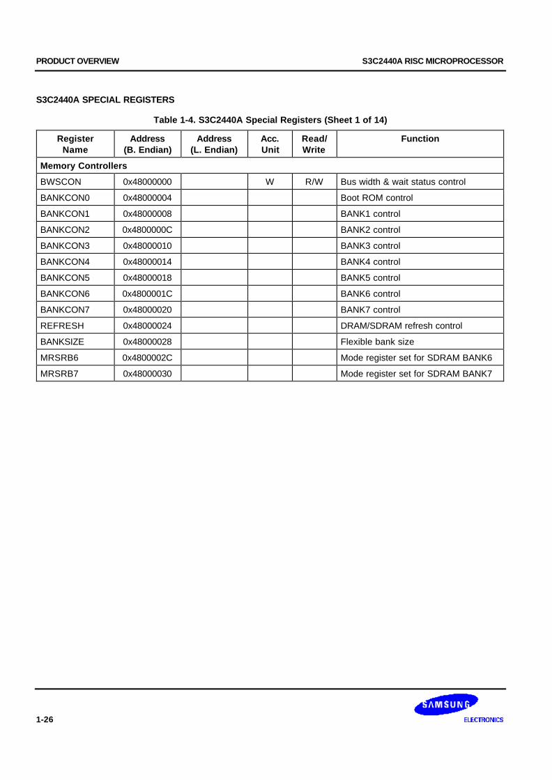
PRODUCT OVERVIEW S3C2440A RISC MICROPROCESSOR
1-26
S3C2440A SPECIAL REGISTERS
Table 1-4. S3C2440A Special Registers (Sheet 1 of 14)
RegisterName
Address(B. Endian)
Address(L. Endian)
Acc.Unit
Read/Write
Function
Memory Controllers
BWSCON 0x48000000 W R/W Bus width & wait status control
BANKCON0 0x48000004 Boot ROM control
BANKCON1 0x48000008 BANK1 control
BANKCON2 0x4800000C BANK2 control
BANKCON3 0x48000010 BANK3 control
BANKCON4 0x48000014 BANK4 control
BANKCON5 0x48000018 BANK5 control
BANKCON6 0x4800001C BANK6 control
BANKCON7 0x48000020 BANK7 control
REFRESH 0x48000024 DRAM/SDRAM refresh control
BANKSIZE 0x48000028 Flexible bank size
MRSRB6 0x4800002C Mode register set for SDRAM BANK6
MRSRB7 0x48000030 Mode register set for SDRAM BANK7

S3C2440A RISC MICROPROCESSOR PRODUCT OVERVIEW
1-27
Table 1-4. S3C2440A Special Registers (Sheet 2 of 14) (Continued)
Register Name Address(B. Endian)
Address(L. Endian)
Acc.Unit
Read/Write
Function
USB Host Controller
HcRevision 0x49000000 ← W Control and status group
HcControl 0x49000004
HcCommonStatus 0x49000008
HcInterruptStatus 0x4900000C
HcInterruptEnable 0x49000010
HcInterruptDisable 0x49000014
HcHCCA 0x49000018 Memory pointer group
HcPeriodCuttentED 0x4900001C
HcControlHeadED 0x49000020
HcControlCurrentED 0x49000024
HcBulkHeadED 0x49000028
HcBulkCurrentED 0x4900002C
HcDoneHead 0x49000030 Frame counter group
HcRmInterval 0x49000034
HcFmRemaining 0x49000038
HcFmNumber 0x4900003C
HcPeriodicStart 0x49000040
HcLSThreshold 0x49000044
HcRhDescriptorA 0x49000048 Root hub group
HcRhDescriptorB 0x4900004C
HcRhStatus 0x49000050
HcRhPortStatus1 0x49000054
HcRhPortStatus2 0x49000058
Interrupt Controller
SRCPND 0X4A000000 ← W R/W Interrupt request status
INTMOD 0X4A000004 W Interrupt mode control
INTMSK 0X4A000008 R/W Interrupt mask control
PRIORITY 0X4A00000C W IRQ priority control
INTPND 0X4A000010 R/W Interrupt request status
INTOFFSET 0X4A000014 R Interrupt request source offset
SUBSRCPND 0X4A000018 R/W Sub source pending
INTSUBMSK 0X4A00001C R/W Interrupt sub mask

PRODUCT OVERVIEW S3C2440A RISC MICROPROCESSOR
1-28
Table 1-4. S3C2440A Special Registers (Sheet 3 of 14) (Continued)
RegisterName
Address(B. Endian)
Address(L. Endian)
Acc.Unit
Read/Write
Function
DMA
DISRC0 0x4B000000 ← W R/W DMA 0 initial source
DISRCC0 0x4B000004 DMA 0 initial source control
DIDST0 0x4B000008 DMA 0 initial destination
DIDSTC0 0x4B00000C DMA 0 initial destination control
DCON0 0x4B000010 DMA 0 control
DSTAT0 0x4B000014 R DMA 0 count
DCSRC0 0x4B000018 DMA 0 current source
DCDST0 0x4B00001C DMA 0 current destination
DMASKTRIG0 0x4B000020 R/W DMA 0 mask trigger
DISRC1 0x4B000040 DMA 1 initial source
DISRCC1 0x4B000044 DMA 1 initial source control
DIDST1 0x4B000048 DMA 1 initial destination
DIDSTC1 0x4B00004C DMA 1 initial destination control
DCON1 0x4B000050 DMA 1 control
DSTAT1 0x4B000054 R DMA 1 count
DCSRC1 0x4B000058 DMA 1 current source
DCDST1 0x4B00005C DMA 1 current destination
DMASKTRIG1 0x4B000060 R/W DMA 1 mask trigger
DISRC2 0x4B000080 DMA 2 initial source
DISRCC2 0x4B000084 DMA 2 initial source control
DIDST2 0x4B000088 DMA 2 initial destination
DIDSTC2 0x4B00008C DMA 2 initial destination control
DCON2 0x4B000090 DMA 2 control
DSTAT2 0x4B000094 R DMA 2 count
DCSRC2 0x4B000098 DMA 2 current source
DCDST2 0x4B00009C DMA 2 current destination
DMASKTRIG2 0x4B0000A0 R/W DMA 2 mask trigger
DISRC3 0x4B0000C0 ← W R/W DMA 3 initial source
DISRCC3 0x4B0000C4 DMA 3 initial source control
DIDST3 0x4B0000C8 DMA 3 initial destination
DIDSTC3 0x4B0000CC DMA 3 initial destination control
DCON3 0x4B0000D0 DMA 3 control
DSTAT3 0x4B0000D4 R DMA 3 count
DCSRC3 0x4B0000D8 DMA 3 current source
DCDST3 0x4B0000DC DMA 3 current destination
DMASKTRIG3 0x4B0000E0 R/W DMA 3 mask trigger
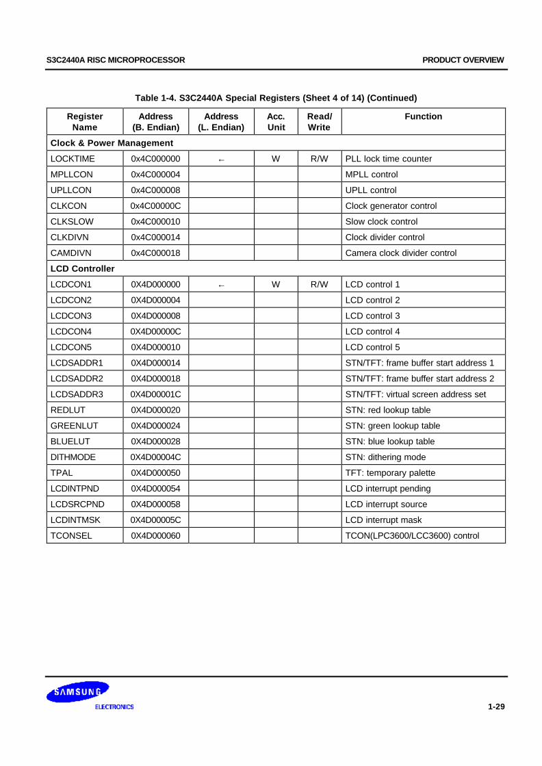
S3C2440A RISC MICROPROCESSOR PRODUCT OVERVIEW
1-29
Table 1-4. S3C2440A Special Registers (Sheet 4 of 14) (Continued)
RegisterName
Address(B. Endian)
Address(L. Endian)
Acc.Unit
Read/Write
Function
Clock & Power Management
LOCKTIME 0x4C000000 ← W R/W PLL lock time counter
MPLLCON 0x4C000004 MPLL control
UPLLCON 0x4C000008 UPLL control
CLKCON 0x4C00000C Clock generator control
CLKSLOW 0x4C000010 Slow clock control
CLKDIVN 0x4C000014 Clock divider control
CAMDIVN 0x4C000018 Camera clock divider control
LCD Controller
LCDCON1 0X4D000000 ← W R/W LCD control 1
LCDCON2 0X4D000004 LCD control 2
LCDCON3 0X4D000008 LCD control 3
LCDCON4 0X4D00000C LCD control 4
LCDCON5 0X4D000010 LCD control 5
LCDSADDR1 0X4D000014 STN/TFT: frame buffer start address 1
LCDSADDR2 0X4D000018 STN/TFT: frame buffer start address 2
LCDSADDR3 0X4D00001C STN/TFT: virtual screen address set
REDLUT 0X4D000020 STN: red lookup table
GREENLUT 0X4D000024 STN: green lookup table
BLUELUT 0X4D000028 STN: blue lookup table
DITHMODE 0X4D00004C STN: dithering mode
TPAL 0X4D000050 TFT: temporary palette
LCDINTPND 0X4D000054 LCD interrupt pending
LCDSRCPND 0X4D000058 LCD interrupt source
LCDINTMSK 0X4D00005C LCD interrupt mask
TCONSEL 0X4D000060 TCON(LPC3600/LCC3600) control

PRODUCT OVERVIEW S3C2440A RISC MICROPROCESSOR
1-30
Table 1-4. S3C2440A Special Registers (Sheet 5 of 14) (Continued)
RegisterName
Address(B. Endian)
Address(L. Endian)
Acc.Unit
Read/Write
Function
NAND Flash
NFCONF 0x4E000000 ← W R/W NAND flash configuration
NFCONT 0x4E000004 NAND flash control
NFCMD 0x4E000008 NAND flash command
NFADDR 0x4E00000C NAND flash address
NFDATA 0x4E000010 NAND flash data
NFMECC0 0x4E000014 NAND flash main area ECC0/1
NFMECC1 0x4E000018 NAND flash main area ECC2/3
NFSECC 0x4E00001C NAND flash spare area ECC
NFSTAT 0x4E000020 NAND flash operation status
NFESTAT0 0x4E000024 NAND flash ECC status for I/O[7:0]
NFESTAT1 0x4E000028 NAND flash ECC status for I/O[15:8]
NFMECC0 0x4E00002C R NAND flash main area ECC0 status
NFMECC1 0x4E000030 NAND flash main area ECC1 status
NFSECC 0x4E000034 NAND flash spare area ECC status
NFSBLK 0x4E000038 R/W NAND flash start block address
NFEBLK 0x4E00003C NAND flash end block address
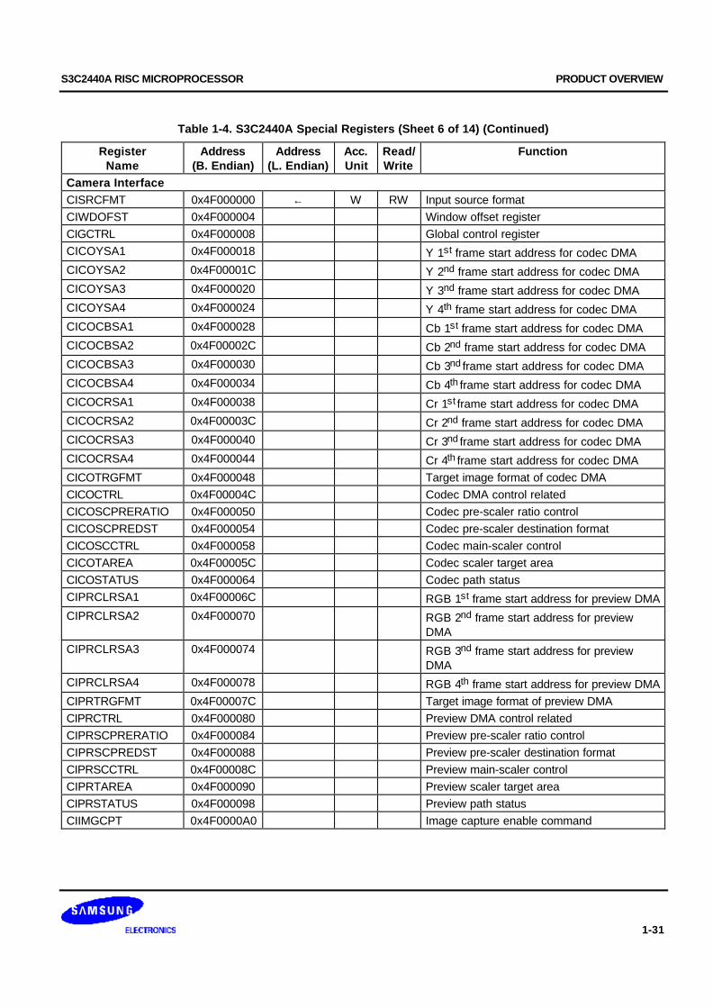
S3C2440A RISC MICROPROCESSOR PRODUCT OVERVIEW
1-31
Table 1-4. S3C2440A Special Registers (Sheet 6 of 14) (Continued)
RegisterName
Address(B. Endian)
Address(L. Endian)
Acc.Unit
Read/Write
Function
Camera InterfaceCISRCFMT 0x4F000000 ← W RW Input source formatCIWDOFST 0x4F000004 Window offset registerCIGCTRL 0x4F000008 Global control registerCICOYSA1 0x4F000018 Y 1st frame start address for codec DMACICOYSA2 0x4F00001C Y 2nd frame start address for codec DMACICOYSA3 0x4F000020 Y 3nd frame start address for codec DMACICOYSA4 0x4F000024 Y 4th frame start address for codec DMACICOCBSA1 0x4F000028 Cb 1st frame start address for codec DMACICOCBSA2 0x4F00002C Cb 2nd frame start address for codec DMACICOCBSA3 0x4F000030 Cb 3nd frame start address for codec DMACICOCBSA4 0x4F000034 Cb 4th frame start address for codec DMACICOCRSA1 0x4F000038 Cr 1st frame start address for codec DMACICOCRSA2 0x4F00003C Cr 2nd frame start address for codec DMACICOCRSA3 0x4F000040 Cr 3nd frame start address for codec DMACICOCRSA4 0x4F000044 Cr 4th frame start address for codec DMACICOTRGFMT 0x4F000048 Target image format of codec DMACICOCTRL 0x4F00004C Codec DMA control relatedCICOSCPRERATIO 0x4F000050 Codec pre-scaler ratio controlCICOSCPREDST 0x4F000054 Codec pre-scaler destination formatCICOSCCTRL 0x4F000058 Codec main-scaler controlCICOTAREA 0x4F00005C Codec scaler target areaCICOSTATUS 0x4F000064 Codec path statusCIPRCLRSA1 0x4F00006C RGB 1st frame start address for preview DMACIPRCLRSA2 0x4F000070 RGB 2nd frame start address for preview
DMACIPRCLRSA3 0x4F000074 RGB 3nd frame start address for preview
DMACIPRCLRSA4 0x4F000078 RGB 4th frame start address for preview DMACIPRTRGFMT 0x4F00007C Target image format of preview DMACIPRCTRL 0x4F000080 Preview DMA control relatedCIPRSCPRERATIO 0x4F000084 Preview pre-scaler ratio controlCIPRSCPREDST 0x4F000088 Preview pre-scaler destination formatCIPRSCCTRL 0x4F00008C Preview main-scaler controlCIPRTAREA 0x4F000090 Preview scaler target areaCIPRSTATUS 0x4F000098 Preview path statusCIIMGCPT 0x4F0000A0 Image capture enable command

PRODUCT OVERVIEW S3C2440A RISC MICROPROCESSOR
1-32
Table 1-4. S3C2440A Special Registers (Sheet 7 of 14) (Continued)
RegisterName
Address(B. Endian)
Address(L. Endian)
Acc. Unit Read/Write
Function
UART
ULCON0 0x50000000 ← W R/W UART 0 line control
UCON0 0x50000004 UART 0 control
UFCON0 0x50000008 UART 0 FIFO control
UMCON0 0x5000000C UART 0 modem control
UTRSTAT0 0x50000010 R UART 0 Tx/Rx status
UERSTAT0 0x50000014 UART 0 Rx error status
UFSTAT0 0x50000018 UART 0 FIFO status
UMSTAT0 0x5000001C UART 0 modem status
UTXH0 0x50000023 0x50000020 B W UART 0 transmission hold
URXH0 0x50000027 0x50000024 R UART 0 receive buffer
UBRDIV0 0x50000028 ← W R/W UART 0 baud rate divisor
ULCON1 0x50004000 UART 1 line control
UCON1 0x50004004 UART 1 control
UFCON1 0x50004008 UART 1 FIFO control
UMCON1 0x5000400C UART 1 modem control
UTRSTAT1 0x50004010 R UART 1 Tx/Rx status
UERSTAT1 0x50004014 UART 1 Rx error status
UFSTAT1 0x50004018 UART 1 FIFO status
UMSTAT1 0x5000401C UART 1 modem status
UTXH1 0x50004023 0x50004020 B W UART 1 transmission hold
URXH1 0x50004027 0x50004024 R UART 1 receive buffer
UBRDIV1 0x50004028 ← W R/W UART 1 baud rate divisor
ULCON2 0x50008000 UART 2 line control
UCON2 0x50008004 UART 2 control
UFCON2 0x50008008 UART 2 FIFO control
UTRSTAT2 0x50008010 R UART 2 Tx/Rx status
UERSTAT2 0x50008014 UART 2 Rx error status
UFSTAT2 0x50008018 UART 2 FIFO status
UTXH2 0x50008023 0x50008020 B W UART 2 transmission hold
URXH2 0x50008027 0x50008024 R UART 2 receive buffer
UBRDIV2 0x50008028 ← W R/W UART 2 baud rate divisor
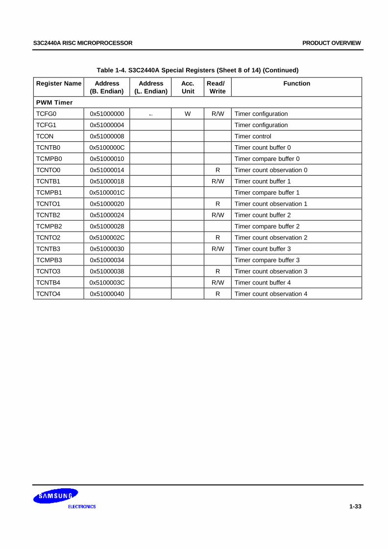
S3C2440A RISC MICROPROCESSOR PRODUCT OVERVIEW
1-33
Table 1-4. S3C2440A Special Registers (Sheet 8 of 14) (Continued)
Register Name Address(B. Endian)
Address(L. Endian)
Acc.Unit
Read/Write
Function
PWM Timer
TCFG0 0x51000000 ← W R/W Timer configuration
TCFG1 0x51000004 Timer configuration
TCON 0x51000008 Timer control
TCNTB0 0x5100000C Timer count buffer 0
TCMPB0 0x51000010 Timer compare buffer 0
TCNTO0 0x51000014 R Timer count observation 0
TCNTB1 0x51000018 R/W Timer count buffer 1
TCMPB1 0x5100001C Timer compare buffer 1
TCNTO1 0x51000020 R Timer count observation 1
TCNTB2 0x51000024 R/W Timer count buffer 2
TCMPB2 0x51000028 Timer compare buffer 2
TCNTO2 0x5100002C R Timer count observation 2
TCNTB3 0x51000030 R/W Timer count buffer 3
TCMPB3 0x51000034 Timer compare buffer 3
TCNTO3 0x51000038 R Timer count observation 3
TCNTB4 0x5100003C R/W Timer count buffer 4
TCNTO4 0x51000040 R Timer count observation 4
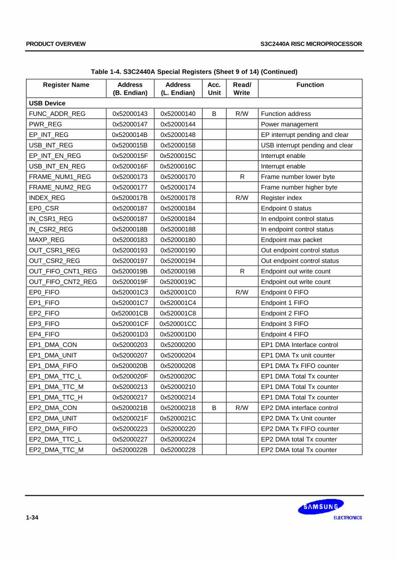
PRODUCT OVERVIEW S3C2440A RISC MICROPROCESSOR
1-34
Table 1-4. S3C2440A Special Registers (Sheet 9 of 14) (Continued)
Register Name Address(B. Endian)
Address(L. Endian)
Acc.Unit
Read/Write
Function
USB Device
FUNC_ADDR_REG 0x52000143 0x52000140 B R/W Function address
PWR_REG 0x52000147 0x52000144 Power management
EP_INT_REG 0x5200014B 0x52000148 EP interrupt pending and clear
USB_INT_REG 0x5200015B 0x52000158 USB interrupt pending and clear
EP_INT_EN_REG 0x5200015F 0x5200015C Interrupt enable
USB_INT_EN_REG 0x5200016F 0x5200016C Interrupt enable
FRAME_NUM1_REG 0x52000173 0x52000170 R Frame number lower byte
FRAME_NUM2_REG 0x52000177 0x52000174 Frame number higher byte
INDEX_REG 0x5200017B 0x52000178 R/W Register index
EP0_CSR 0x52000187 0x52000184 Endpoint 0 status
IN_CSR1_REG 0x52000187 0x52000184 In endpoint control status
IN_CSR2_REG 0x5200018B 0x52000188 In endpoint control status
MAXP_REG 0x52000183 0x52000180 Endpoint max packet
OUT_CSR1_REG 0x52000193 0x52000190 Out endpoint control status
OUT_CSR2_REG 0x52000197 0x52000194 Out endpoint control status
OUT_FIFO_CNT1_REG 0x5200019B 0x52000198 R Endpoint out write count
OUT_FIFO_CNT2_REG 0x5200019F 0x5200019C Endpoint out write count
EP0_FIFO 0x520001C3 0x520001C0 R/W Endpoint 0 FIFO
EP1_FIFO 0x520001C7 0x520001C4 Endpoint 1 FIFO
EP2_FIFO 0x520001CB 0x520001C8 Endpoint 2 FIFO
EP3_FIFO 0x520001CF 0x520001CC Endpoint 3 FIFO
EP4_FIFO 0x520001D3 0x520001D0 Endpoint 4 FIFO
EP1_DMA_CON 0x52000203 0x52000200 EP1 DMA Interface control
EP1_DMA_UNIT 0x52000207 0x52000204 EP1 DMA Tx unit counter
EP1_DMA_FIFO 0x5200020B 0x52000208 EP1 DMA Tx FIFO counter
EP1_DMA_TTC_L 0x5200020F 0x5200020C EP1 DMA Total Tx counter
EP1_DMA_TTC_M 0x52000213 0x52000210 EP1 DMA Total Tx counter
EP1_DMA_TTC_H 0x52000217 0x52000214 EP1 DMA Total Tx counter
EP2_DMA_CON 0x5200021B 0x52000218 B R/W EP2 DMA interface control
EP2_DMA_UNIT 0x5200021F 0x5200021C EP2 DMA Tx Unit counter
EP2_DMA_FIFO 0x52000223 0x52000220 EP2 DMA Tx FIFO counter
EP2_DMA_TTC_L 0x52000227 0x52000224 EP2 DMA total Tx counter
EP2_DMA_TTC_M 0x5200022B 0x52000228 EP2 DMA total Tx counter

S3C2440A RISC MICROPROCESSOR PRODUCT OVERVIEW
1-35
Table 1-4. S3C2440A Special Registers (Sheet 10 of 14) (Continued)
Register Name Address(B. Endian)
Address(L. Endian)
Acc.Unit
Read/Write
Function
USB Device (Continued)
EP2_DMA_TTC_H 0x5200022F 0x5200022C EP2 DMA Total Tx counter
EP3_DMA_CON 0x52000243 0x52000240 EP3 DMA Interface control
EP3_DMA_UNIT 0x52000247 0x52000244 EP3 DMA Tx Unit counter
EP3_DMA_FIFO 0x5200024B 0x52000248 EP3 DMA Tx FIFO counter
EP3_DMA_TTC_L 0x5200024F 0x5200024C EP3 DMA Total Tx counter
EP3_DMA_TTC_M 0x52000253 0x52000250 EP3 DMA Total Tx counter
EP3_DMA_TTC_H 0x52000257 0x52000254 EP3 DMA Total Tx counter
EP4_DMA_CON 0x5200025B 0x52000258 EP4 DMA Interface control
EP4_DMA_UNIT 0x5200025F 0x5200025C EP4 DMA Tx Unit counter
EP4_DMA_FIFO 0x52000263 0x52000260 EP4 DMA Tx FIFO counter
EP4_DMA_TTC_L 0x52000267 0x52000264 EP4 DMA Total Tx counter
EP4_DMA_TTC_M 0x5200026B 0x52000268 EP4 DMA Total Tx counter
EP4_DMA_TTC_H 0x5200026F 0x5200026C EP4 DMA Total Tx counter
Watchdog Timer
WTCON 0x53000000 ← W R/W Watchdog timer mode
WTDAT 0x53000004 Watchdog timer data
WTCNT 0x53000008 Watchdog timer count
IIC
IICCON 0x54000000 ← W R/W IIC control
IICSTAT 0x54000004 IIC status
IICADD 0x54000008 IIC address
IICDS 0x5400000C IIC data shift
IICLC 0x54000010 IIC multi-master line control
IIS
IISCON 0x55000000,02 0x55000000 HW,W R/W IIS control
IISMOD 0x55000004,06 0x55000004 IIS mode
IISPSR 0x55000008,0A 0x55000008 IIS prescaler
IISFCON 0x5500000C,0E 0x5500000C IIS FIFO control
IISFIFO 0x55000012 0x55000010 HW IIS FIFO entry
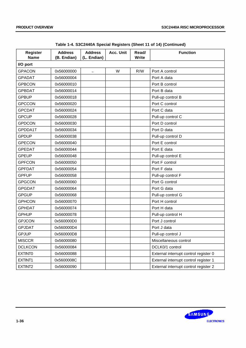
PRODUCT OVERVIEW S3C2440A RISC MICROPROCESSOR
1-36
Table 1-4. S3C2440A Special Registers (Sheet 11 of 14) (Continued)
RegisterName
Address(B. Endian)
Address(L. Endian)
Acc. Unit Read/Write
Function
I/O port
GPACON 0x56000000 ← W R/W Port A control
GPADAT 0x56000004 Port A data
GPBCON 0x56000010 Port B control
GPBDAT 0x56000014 Port B data
GPBUP 0x56000018 Pull-up control B
GPCCON 0x56000020 Port C control
GPCDAT 0x56000024 Port C data
GPCUP 0x56000028 Pull-up control C
GPDCON 0x56000030 Port D control
GPDDA1T 0x56000034 Port D data
GPDUP 0x56000038 Pull-up control D
GPECON 0x56000040 Port E control
GPEDAT 0x56000044 Port E data
GPEUP 0x56000048 Pull-up control E
GPFCON 0x56000050 Port F control
GPFDAT 0x56000054 Port F data
GPFUP 0x56000058 Pull-up control F
GPGCON 0x56000060 Port G control
GPGDAT 0x56000064 Port G data
GPGUP 0x56000068 Pull-up control G
GPHCON 0x56000070 Port H control
GPHDAT 0x56000074 Port H data
GPHUP 0x56000078 Pull-up control H
GPJCON 0x560000D0 Port J control
GPJDAT 0x560000D4 Port J data
GPJUP 0x560000D8 Pull-up control J
MISCCR 0x56000080 Miscellaneous control
DCLKCON 0x56000084 DCLK0/1 control
EXTINT0 0x56000088 External interrupt control register 0
EXTINT1 0x5600008C External interrupt control register 1
EXTINT2 0x56000090 External interrupt control register 2
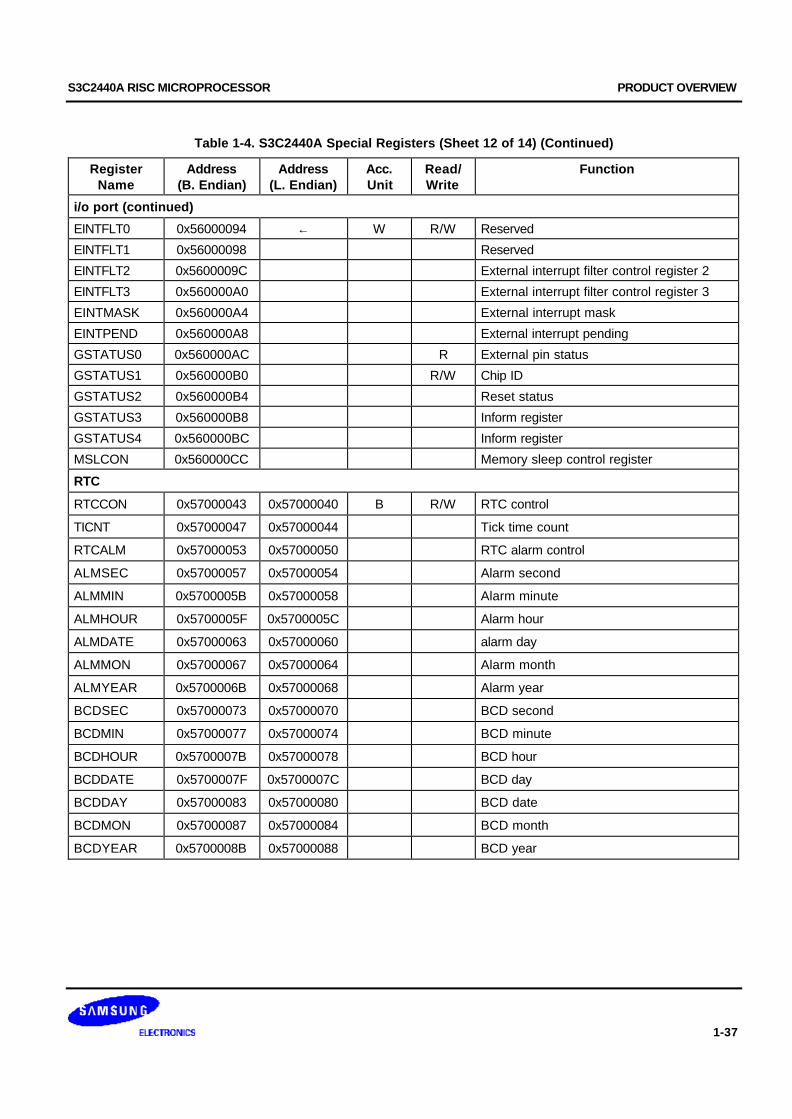
S3C2440A RISC MICROPROCESSOR PRODUCT OVERVIEW
1-37
Table 1-4. S3C2440A Special Registers (Sheet 12 of 14) (Continued)
RegisterName
Address(B. Endian)
Address(L. Endian)
Acc.Unit
Read/Write
Function
i/o port (continued)
EINTFLT0 0x56000094 ← W R/W Reserved
EINTFLT1 0x56000098 Reserved
EINTFLT2 0x5600009C External interrupt filter control register 2
EINTFLT3 0x560000A0 External interrupt filter control register 3
EINTMASK 0x560000A4 External interrupt mask
EINTPEND 0x560000A8 External interrupt pending
GSTATUS0 0x560000AC R External pin status
GSTATUS1 0x560000B0 R/W Chip ID
GSTATUS2 0x560000B4 Reset status
GSTATUS3 0x560000B8 Inform register
GSTATUS4 0x560000BC Inform register
MSLCON 0x560000CC Memory sleep control register
RTC
RTCCON 0x57000043 0x57000040 B R/W RTC control
TICNT 0x57000047 0x57000044 Tick time count
RTCALM 0x57000053 0x57000050 RTC alarm control
ALMSEC 0x57000057 0x57000054 Alarm second
ALMMIN 0x5700005B 0x57000058 Alarm minute
ALMHOUR 0x5700005F 0x5700005C Alarm hour
ALMDATE 0x57000063 0x57000060 alarm day
ALMMON 0x57000067 0x57000064 Alarm month
ALMYEAR 0x5700006B 0x57000068 Alarm year
BCDSEC 0x57000073 0x57000070 BCD second
BCDMIN 0x57000077 0x57000074 BCD minute
BCDHOUR 0x5700007B 0x57000078 BCD hour
BCDDATE 0x5700007F 0x5700007C BCD day
BCDDAY 0x57000083 0x57000080 BCD date
BCDMON 0x57000087 0x57000084 BCD month
BCDYEAR 0x5700008B 0x57000088 BCD year

PRODUCT OVERVIEW S3C2440A RISC MICROPROCESSOR
1-38
Table 1-4. S3C2440A Special Registers (Sheet 13 of 14) (Continued)
RegisterName
Address(B. Endian)
Address(L. Endian)
Acc. Unit Read/Write
Function
A/D Converter
ADCCON 0x58000000 ← W R/W ADC control
ADCTSC 0x58000004 ADC touch screen control
ADCDLY 0x58000008 ADC start or interval delay
ADCDAT0 0x5800000C R ADC conversion data
ADCDAT1 0x58000010 ADC conversion data
ADCUPDN 0x58000014 R/W Stylus up or down interrupt status
SPI
SPCON0,1 0x59000000,20 ← W R/W SPI control
SPSTA0,1 0x59000004,24 R SPI status
SPPIN0,1 0x59000008,28 R/W SPI pin control
SPPRE0,1 0x5900000C,2C SPI baud rate prescaler
SPTDAT0,1 0x59000010,30 SPI Tx data
SPRDAT0,1 0x59000014,34 R SPI Rx data
SD Interface
SDICON 0x5A000000 ← W R/W SDI control
SDIPRE 0x5A000004 SDI baud rate prescaler
SDICARG 0x5A000008 SDI command argument
SDICCON 0x5A00000C SDI command control
SDICSTA 0x5A000010 R/(C) SDI command status
SDIRSP0 0x5A000014 R SDI response
SDIRSP1 0x5A000018 SDI response
SDIRSP2 0x5A00001C SDI response
SDIRSP3 0x5A000020 SDI response
SDIDTIMER 0x5A000024 R/W SDI data / busy timer
SDIBSIZE 0x5A000028 SDI block size
SDIDCON 0x5A00002C SDI data control
SDIDCNT 0x5A000030 R SDI data remain counter
SDIDSTA 0x5A000034 R/(C) SDI data status
SDIFSTA 0x5A000038 R SDI FIFO status
SDIIMSK 0x5A00003C ← W SDI interrupt mask
SDIDAT 0x5A000043 0x5A000040 B R/W SDI data
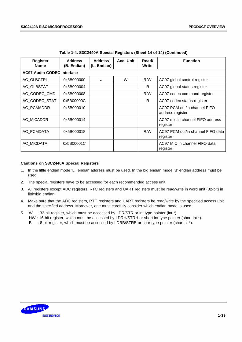
S3C2440A RISC MICROPROCESSOR PRODUCT OVERVIEW
1-39
Table 1-4. S3C2440A Special Registers (Sheet 14 of 14) (Continued)
RegisterName
Address(B. Endian)
Address(L. Endian)
Acc. Unit Read/Write
Function
AC97 Audio-CODEC Interface
AC_GLBCTRL 0x5B000000 ← W R/W AC97 global control register
AC_GLBSTAT 0x5B000004 R AC97 global status register
AC_CODEC_CMD 0x5B000008 R/W AC97 codec command register
AC_CODEC_STAT 0x5B00000C R AC97 codec status register
AC_PCMADDR 0x5B000010 AC97 PCM out/in channel FIFOaddress register
AC_MICADDR 0x5B000014 AC97 mic in channel FIFO addressregister
AC_PCMDATA 0x5B000018 R/W AC97 PCM out/in channel FIFO dataregister
AC_MICDATA 0x5B00001C AC97 MIC in channel FIFO dataregister
Cautions on S3C2440A Special Registers
1. In the little endian mode ‘L’, endian address must be used. In the big endian mode ‘B’ endian address must beused.
2. The special registers have to be accessed for each recommended access unit.
3. All registers except ADC registers, RTC registers and UART registers must be read/write in word unit (32-bit) inlittle/big endian.
4. Make sure that the ADC registers, RTC registers and UART registers be read/write by the specified access unitand the specified address. Moreover, one must carefully consider which endian mode is used.
5. W : 32-bit register, which must be accessed by LDR/STR or int type pointer (int *).HW : 16-bit register, which must be accessed by LDRH/STRH or short int type pointer (short int *).B : 8-bit register, which must be accessed by LDRB/STRB or char type pointer (char int *).
S3C2440A RISC MICROPROCESSOR PROGRAMMER'S MODEL
2-1
2 PROGRAMMER'S MODEL
OVERVIEW
S3C2440A is developed using the advanced ARM920T core, which has been designed by Advanced RISC Machines, Ltd.
PROCESSOR OPERATING STATES
From the programmer's point of view, the ARM920T can be in one of the two states:
• ARM state which executes 32-bit, word-aligned ARM instructions
• THUMB state is a state which can execute 16-bit, halfword-aligned THUMB instructions. In this state, the PC uses bit 1 to select between alternate halfwords
NOTE
Transition between these two states does not affect the processor mode or the contents of the registers.
SWITCHING STATE
Entering THUMB State
Entry into THUMB state can be achieved by executing a BX instruction with the state bit (bit 0) set in the operand register.
Transition to THUMB state will also occur automatically on return from an exception (IRQ, FIQ, UNDEF, ABORT, SWI etc.), if the exception is entered with the processor in THUMB state.
Entering ARM State
Entry into ARM state can be done by the following methods:-
• On execution of the BX instruction with the state bit clear in the operand register.
• On the processor taking an exception (IRQ, FIQ, RESET, UNDEF, ABORT, SWI etc.). In this case, the PC is placed in the exception mode's link register, and execution commences at the exception's vector address.
MEMORY FORMATS
ARM920T views memory as a linear collection of bytes numbered upwards from zero. Bytes 0 to 3 hold the first stored word, bytes 4 to 7 the second and so on. ARM920T can treat words in memory as being stored either in Big-Endian or Little-Endian format.

PROGRAMMER'S MODEL S3C2440A RISC MICROPROCESSOR
2-2
BIG-ENDIAN FORMAT
In Big-Endian format, the most significant byte of a word is stored at the lowest numbered byte and the least significant byte at the highest numbered byte. Byte 0 of the memory system is therefore connected to data lines 31 through 24.
31 24
8
4
0
23 16
9
5
1
10
6
2
11
7
3
15 8 7 0
4
0
8
Higher Address
Lower Address
Word Address
Most significant byte is at lowest addressWord is addressed by byte address of most significant byte
Figure 2-1. Big-Endian Addresses of Bytes within Words
LITTLE-ENDIAN FORMAT
In Little-Endian format, the lowest numbered byte in a word is considered the word's least significant byte, and the highest numbered byte the most significant. Byte 0 of the memory system is therefore connected to data lines 7 through 0.
31 24
11
7
3
23 16
10
6
2
9
5
1
8
4
0
15 8 7 0
4
0
8
Higher Address
Lower Address
Word Address
Least significant byte is at lowest addressWord is addressed by byte address of least significant byte
Figure 2-2. Little-Endian Addresses of Bytes within Words
INSTRUCTION LENGTH
Instructions are either 32 bits long (in ARM state) or 16 bits long (in THUMB state).
Data Types
ARM920T supports byte (8-bit), halfword (16-bit) and word (32-bit) data types. Words must be aligned to four-byte boundaries and half words to two-byte boundaries.
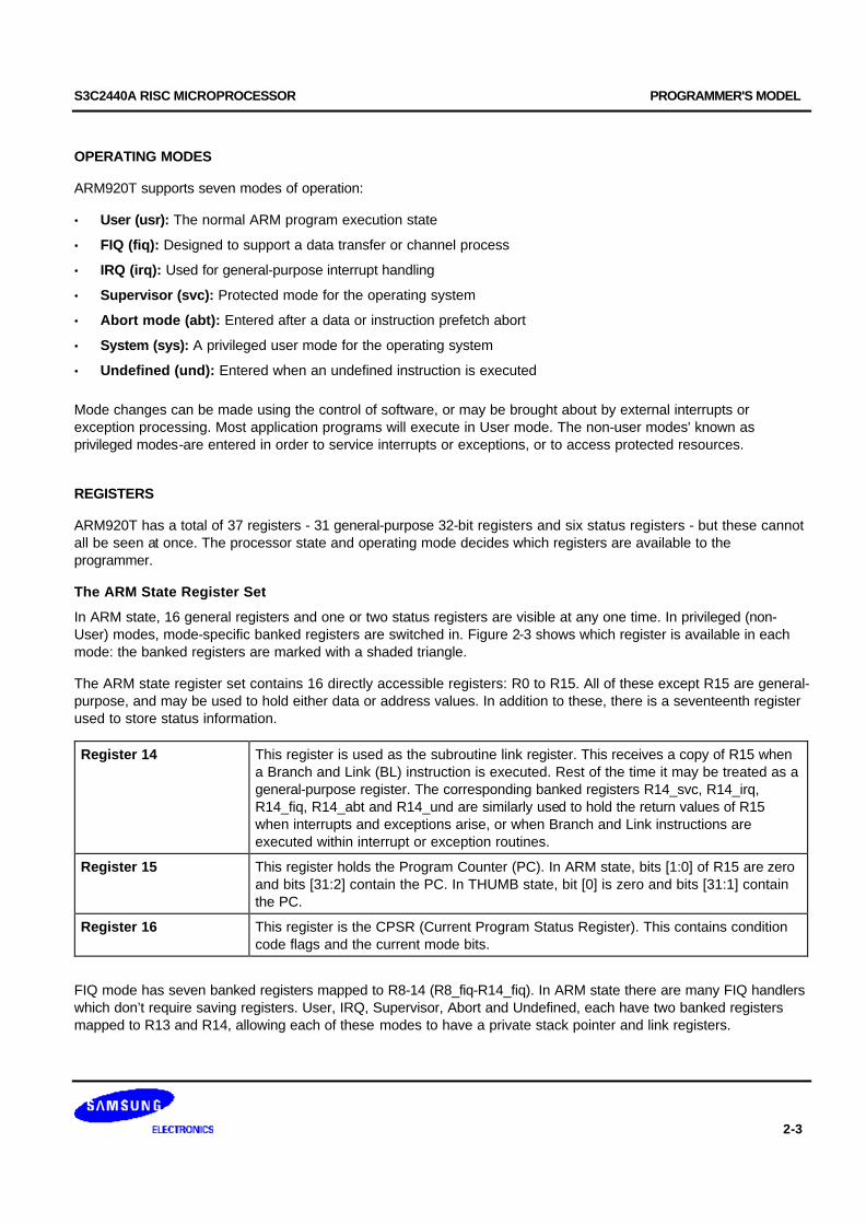
S3C2440A RISC MICROPROCESSOR PROGRAMMER'S MODEL
2-3
OPERATING MODES
ARM920T supports seven modes of operation:
• User (usr): The normal ARM program execution state
• FIQ (fiq): Designed to support a data transfer or channel process
• IRQ (irq): Used for general-purpose interrupt handling
• Supervisor (svc): Protected mode for the operating system
• Abort mode (abt): Entered after a data or instruction prefetch abort
• System (sys): A privileged user mode for the operating system
• Undefined (und): Entered when an undefined instruction is executed
Mode changes can be made using the control of software, or may be brought about by external interrupts or exception processing. Most application programs will execute in User mode. The non-user modes' known as privileged modes-are entered in order to service interrupts or exceptions, or to access protected resources.
REGISTERS
ARM920T has a total of 37 registers - 31 general-purpose 32-bit registers and six status registers - but these cannot all be seen at once. The processor state and operating mode decides which registers are available to the programmer.
The ARM State Register Set
In ARM state, 16 general registers and one or two status registers are visible at any one time. In privileged (non-User) modes, mode-specific banked registers are switched in. Figure 2-3 shows which register is available in each mode: the banked registers are marked with a shaded triangle.
The ARM state register set contains 16 directly accessible registers: R0 to R15. All of these except R15 are general-purpose, and may be used to hold either data or address values. In addition to these, there is a seventeenth register used to store status information.
Register 14 This register is used as the subroutine link register. This receives a copy of R15 when a Branch and Link (BL) instruction is executed. Rest of the time it may be treated as a general-purpose register. The corresponding banked registers R14_svc, R14_irq, R14_fiq, R14_abt and R14_und are similarly used to hold the return values of R15 when interrupts and exceptions arise, or when Branch and Link instructions are executed within interrupt or exception routines.
Register 15 This register holds the Program Counter (PC). In ARM state, bits [1:0] of R15 are zero and bits [31:2] contain the PC. In THUMB state, bit [0] is zero and bits [31:1] contain the PC.
Register 16 This register is the CPSR (Current Program Status Register). This contains condition code flags and the current mode bits.
FIQ mode has seven banked registers mapped to R8-14 (R8_fiq-R14_fiq). In ARM state there are many FIQ handlers which don’t require saving registers. User, IRQ, Supervisor, Abort and Undefined, each have two banked registers mapped to R13 and R14, allowing each of these modes to have a private stack pointer and link registers.

PROGRAMMER'S MODEL S3C2440A RISC MICROPROCESSOR
2-4
r0r1r2r3
r4r5r6r7
r9r8
r10r11r12r13r14r15 (PC)
r0r1r2r3
r4r5r6r7
r9r8
r10r11r12r13_ svc
r14_ svc
r15 (PC)
r0r1r2r3
r4r5r6r7
r9_ fiq
r10_ fiq
r11_ fiq
r12_ fiq
r13_ fiq
r14_ fiq
r15 (PC)
r8_ fiq
r0r1r2r3
r4r5r6r7
r9r8
r10r11r12r13_ abt
r14_ abt
r15 (PC)
r0r1r2r3
r4r5r6r7
r9r8
r10r11r12r13_ irq
r14_ irq
r15 (PC)
r0r1r2r3
r4r5r6r7
r9r8
r10r11r12r13_ und
r14_ und
r15 (PC)
System & User FIQ Supervisor IRQAbort Undefined
ARM State General Registers and Program Counter
ARM State Program Status Registers
CPSR CPSRSPSR_fiq
CPSRSPSR_svc
CPSRSPSR_abt
CPSRSPSR_irq
CPSRSPSR_und
= banked register
Figure 2-3. Register Organization in ARM State
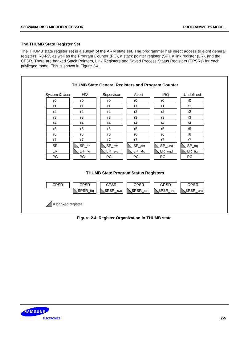
S3C2440A RISC MICROPROCESSOR PROGRAMMER'S MODEL
2-5
The THUMB State Register Set
The THUMB state register set is a subset of the ARM state set. The programmer has direct access to eight general registers, R0-R7, as well as the Program Counter (PC), a stack pointer register (SP), a link register (LR), and the CPSR. There are banked Stack Pointers, Link Registers and Saved Process Status Registers (SPSRs) for each privileged mode. This is shown in Figure 2-4.
r0r1r2
r3r4
r5r6r7
LRSP
PC
System & User FIQ Supervisor IRQAbort Undefined
THUMB State General Registers and Program Counter
THUMB State Program Status Registers
CPSR CPSR
SPSR_fiq
CPSR
SPSR_ svc
CPSR
SPSR_abt
CPSR
SPSR_ irq
CPSR
SPSR_und
= banked register
LR_ fiq
r0r1r2
r3r4
r5r6r7
SP_fiq
PCLR_svc
r0r1r2
r3r4
r5r6r7
SP_svc
PCLR_und
r0r1r2
r3r4
r5r6r7
SP_und
PCLR_fiq
r0r1r2
r3r4
r5r6r7
SP_fiq
PCLR_abt
r0r1r2
r3r4
r5r6r7
SP_abt
PC
Figure 2-4. Register Organization in THUMB state

PROGRAMMER'S MODEL S3C2440A RISC MICROPROCESSOR
2-6
The relationship between ARM and THUMB state registers
The relationship between ARM and THUMB state registers are as below:-
• THUMB state R0-R7 and ARM state R0-R7 are identical
• THUMB state CPSR and SPSRs and ARM state CPSR and SPSRs are identical
• THUMB state SP maps onto ARM state R13
• THUMB state LR maps onto ARM state R14
• The THUMB state Program Counter maps onto the ARM state Program Counter (R15)
This relationship is shown in Figure 2-5.
THUMB State
(CPSR)(SPSR)
Stack Pointer (r13)Link Register (r14)
Program Counter (r15)
r0r1r2r3r4r5r6r7r8r9r10r11r12
(CPSR)(SPSR)
Stack Pointer (SP)Link Register (LR)
Program Counter (PC)
r0r1r2r3r4r5r6r7
ARM State
Lo-R
egis
ters
Hi-R
egis
ters
Figure 2-5. Mapping of THUMB State Registers onto ARM State Registers

S3C2440A RISC MICROPROCESSOR PROGRAMMER'S MODEL
2-7
Accessing Hi-Registers in THUMB State
In THUMB state, registers R8-R15 ("Hi registers") are not part of the standard register set. However, the assembly language programmer has limited access to them, and can use them for fast temporary storage.
A value may be transferred from a register in the range R0-R7 (a Lo register) to a Hi register and from a Hi register to a Lo register, using special variants of the MOV instruction. Hi register values can also be compared against or added to Lo register values with the CMP and ADD instructions. For more information, Please refer to Figure 3-34.
THE PROGRAM STATUS REGISTERS
The ARM920T contains a Current Program Status Register (CPSR), plus five Saved Program Status Registers (SPSRs) for use by exception handlers. These register's functions are:
• Hold information about the most recently performed ALU operation
• Control the enabling and disabling of interrupts
• Set the processor operating mode
The arrangement of bits is shown in Figure 2-6.
31
Condition Code Flags
Overflow
N Z C V I F T M4 M3 M2 M1 M0
30 29 2728 26 25 24 23 8 7 6 5 4 3 2 1 0
(Resverved) Control Bits
Carry/Borrow/ExtendZeroNegative/Less Than
Mode bitsState bitsFIQ disableIRQ disable
~ ~~ ~
Figure 2-6. Program Status Register Format
PROGRAMMER'S MODEL S3C2440A RISC MICROPROCESSOR
2-8
The Condition Code Flags
The N, Z, C and V bits are the condition code flags. These may be changed as a result of arithmetic and logical operations, and may be tested to determine whether an instruction should be executed.
In ARM state, all instructions may be executed conditionally: see Table 3-2 for details.
In THUMB state, only the Branch instruction is capable of conditional execution: see Figure 3-46 for details.
The Control Bits
The bottom 8 bits of a PSR (incorporating I, F, T and M[4:0]) are known collectively as the control bits. These will be changed when an exception arises. If the processor is operating in a privileged mode, they can also be manipulated by software.
The T bit This reflects the operating state. When this bit is set, the processor is executed in THUMB state, or otherwise it is executing in ARM state. This is reflected on the TBIT external signal.
Note: That the software must never change the state of the TBIT in the CPSR. If this happens, the processor will enter an unpredictable state.
Interrupt disable bits I and F bits are the interrupt disable bits. When set, these disable the IRQ and FIQ interrupts respectively.
The mode bits The M4, M3, M2, M1 and M0 bits (M[4:0]) are the mode bits. These determine the processor's operating mode, as shown in Table 2-1. Not all combinations of the mode bits define a valid processor mode. Only those explicitly described shall be used. The user should be aware that if any illegal value is programmed into the mode bits, M[4:0], then the processor will enter an unrecoverable state. If this occurs, reset should be applied.
Reserved bits
The remaining bits in the PSRs are reserved. When changing a PSR's flag or control bits, you must ensure that these unused bits are not altered. Also, your program should not rely on them containing specific values, since in future processors they may read as one or zero.

S3C2440A RISC MICROPROCESSOR PROGRAMMER'S MODEL
2-9
Table 2-1. PSR Mode Bit Values
M[4:0] Mode Visible THUMB state registers Visible ARM state registers
10000 User R7..R0, LR, SP PC, CPSR
R14..R0, PC, CPSR
10001 FIQ R7..R0, LR_fiq, SP_fiq PC, CPSR, SPSR_fiq
R7..R0, R14_fiq..R8_fiq, PC, CPSR, SPSR_fiq
10010 IRQ R7..R0, LR_irq, SP_irq PC, CPSR, SPSR_irq
R12..R0, R14_irq, R13_irq, PC, CPSR, SPSR_irq
10011 Supervisor R7..R0, LR_svc, SP_svc, PC, CPSR, SPSR_svc
R12..R0, R14_svc, R13_svc, PC, CPSR, SPSR_svc
10111 Abort R7..R0, LR_abt, SP_abt, PC, CPSR, SPSR_abt
R12..R0, R14_abt, R13_abt, PC, CPSR, SPSR_abt
11011 Undefined R7..R0 LR_und, SP_und, PC, CPSR, SPSR_und
R12..R0, R14_und, R13_und, PC, CPSR
11111 System R7..R0, LR, SP PC, CPSR
R14..R0, PC, CPSR
Reserved bits The remaining bits in the PSR's are reserved. While changing a PSR's flag or control bits, you must ensure that these unused bits are not altered. Also, your program should not rely on them containing specific values, since in future processors they may read as one or zero.

PROGRAMMER'S MODEL S3C2440A RISC MICROPROCESSOR
2-10
EXCEPTIONS
Exceptions arise whenever the normal flow of a program has to be halted temporarily, for example to service an interrupt from a peripheral. Before an exception can be handled, the current processor state must be preserved so that the original program can resume when the handler routine has finished.
It is possible for several exceptions to arise at the same time. If this happens, they are dealt with in a fixed order. See Exception Priorities on page 2-14.
Action on Entering an Exception
While handling an exception, the ARM920T does following activities:
1. Preserves the address of the next instruction in the appropriate Link Register. If the exception has been entered from ARM state, then the address of the next instruction is copied into the Link Register (that is, current PC + 4 or PC + 8 depending on the exception. See Table 2-2 on for details). If the exception has been entered from THUMB state, then the value written into the Link Register is the current PC offset by a value such that the program resumes from the correct place on return from the exception. This means that the exception handler need not determine which state the exception was entered from. For example, in the case of SWI, MOVS PC, R14_svc will always return to the next instruction regardless of whether the SWI was executed in ARM or THUMB state.
2. Copies the CPSR into the appropriate SPSR
3. Forces the CPSR mode bits to a value which depends on the exception
4. Forces the PC to fetch the next instruction from the relevant exception vector
It may also set the interrupt disable flags to prevent otherwise unmanageable nestings of exceptions.
If the processor is in THUMB state when an exception occurs, it will automatically switch into ARM state when the PC is loaded with the exception vector address.
Action on Leaving an Exception
On completion, the exception handler:
1. Moves the Link Register, minus an offset where appropriate, to the PC. (The offset will vary depending on the type of exception.)
2. Copies the SPSR back to the CPSR
3. Clears the interrupt disable flags, if they were set on entry
NOTE
An explicit switch back to THUMB state is never needed, since restoring the CPSR from the SPSR automatically sets the T bit to the value it held immediately prior to the exception.
S3C2440A RISC MICROPROCESSOR PROGRAMMER'S MODEL
2-11
Exception Entry/Exit Summary
Table 2-2 summarizes the PC value preserved in the relevant R14 on exception entry, and the recommended instruction for exiting the exception handler.
Table 2-2. Exception Entry/Exit
Return Instruction Previous State Notes
ARM R14_x THUMB R14_x
BL MOV PC, R14 PC + 4 PC + 2 (1)
SWI MOVS PC, R14_svc PC + 4 PC + 2 (1)
UDEF MOVS PC, R14_und PC + 4 PC + 2 (1)
FIQ SUBS PC, R14_fiq, #4 PC + 4 PC + 4 (2)
IRQ SUBS PC, R14_irq, #4 PC + 4 PC + 4 (2)
PABT SUBS PC, R14_abt, #4 PC + 4 PC + 4 (1)
DABT SUBS PC, R14_abt, #8 PC + 8 PC + 8 (3)
RESET NA – – (4)
NOTES: 1. Where PC is the address of the BL/SWI/Undefined Instruction fetch which had the prefetch abort. 2. Where PC is the address of the instruction which did not get executed since the FIQ or IRQ took priority. 3. Where PC is the address of the Load or Store instruction which generated the data abort. 4. The value saved in R14_svc upon reset is unpredictable.
FIQ
The FIQ (Fast Interrupt Request) exception is designed to support a data transfer or channel process, and in ARM state has sufficient private registers to remove the need for register saving (thus minimizing the overhead of context switching).
FIQ is externally generated by taking the nFIQ input LOW. This input can except either synchronous or asynchronous transitions, depending on the state of the ISYNC input signal. When ISYNC is LOW, nFIQ and nIRQ are considered asynchronous, and a cycle delay for synchronization is incurred before the interrupt can affect the processor flow.
Irrespective of whether the exception was entered from ARM or Thumb state, a FIQ handler should leave the interrupt by executing
SUBS PC,R14_fiq,#4
FIQ may be disabled by setting the CPSR's F flag (but note that this is not possible from User mode). If the F flag is clear, ARM920T checks for a LOW level on the output of the FIQ synchronizer at the end of each instruction.

PROGRAMMER'S MODEL S3C2440A RISC MICROPROCESSOR
2-12
IRQ
The IRQ (Interrupt Request) exception is a normal interrupt caused by a LOW level on the nIRQ input. IRQ has a lower priority than FIQ and is masked out when a FIQ sequence is entered. It may be disabled at any time by setting I bit in the CPSR, though this can only be done from a privileged (non-User) mode.
Irrespective of whether the exception was entered from ARM or Thumb state, an IRQ handler should return from the interrupt by executing
SUBS PC,R14_irq,#4
Abort
An abort indicates that the current memory access cannot be completed. It can be signaled by the external ABORT input. ARM920T checks for the abort exception during memory access cycles.
There are two types of abort:
• Prefetch Abort: occurs during an instruction prefetch.
• Data Abort: occurs during a data access.
If a prefetch abort occurs, the prefetched instruction is marked as invalid, but the exception will not be taken until the instruction reaches the head of the pipeline. If the instruction is not executed – the abort doesn’t take place because a branch occurs while it is in the pipeline -.
If a data abort occurs, the action taken depends on the instruction type:
• Single data transfer instructions (LDR, STR) write back modified base registers: the Abort handler must be aware of this.
• The swap instruction (SWP) is aborted as though it had not been executed.
• Block data transfer instructions (LDM, STM) complete. If write-back is set, the base is updated. If the instruction would have overwritten the base with data (ie it has the base in the transfer list), the overwriting is prevented. All register overwriting is prevented after an abort is indicated, which means in particular that R15 (always the last register to be transferred) is preserved in an aborted LDM instruction.
The abort mechanism allows the implementation of a demand paged virtual memory system. In such a system the processor is allowed to generate arbitrary addresses. When the data at an address is unavailable, the Memory Management Unit (MMU) signals an abort. The abort handler must then work out the cause of the abort, make the requested data available, and retry the aborted instruction. The application program needs no knowledge of the amount of memory available to it, nor is its state in any way affected by the abort.
After fixing the reason for the abort, the handler should execute the following irrespective of the state (ARM or Thumb):
SUBS PC,R14_abt,#4 ; for a prefetch abort, or SUBS PC,R14_abt,#8 ; for a data abort
This restores both the PC and the CPSR, and retries the aborted instruction.
S3C2440A RISC MICROPROCESSOR PROGRAMMER'S MODEL
2-13
Software Interrupt
The Software Interrupt Instruction (SWI) is used for entering Supervisor mode, usually to request a particular supervisor function. A SWI handler should return by executing the following irrespective of the state (ARM or Thumb):
MOV PC,R14_svc
This restores the PC and CPSR, and returns to the instruction following the SWI.
NOTE
nFIQ, nIRQ, ISYNC, LOCK, BIGEND, and ABORT pins exist only in the ARM920T CPU core.
Undefined Instruction
When ARM920T comes across an instruction which cannot be handled, it takes the undefined instruction trap. This mechanism may be used to extend either the THUMB or ARM instruction set by software emulation.
After emulating the failed instruction, the trap handler should execute the following irrespective of the state (ARM or Thumb):
MOVS PC,R14_und
This restores the CPSR and returns to the instruction following the undefined instruction.
Exception Vectors
The following table shows the exception vector addresses.
Table 2-3. Exception Vectors
Address Exception Mode in Entry
0x00000000 Reset Supervisor
0x00000004 Undefined instruction Undefined
0x00000008 Software Interrupt Supervisor
0x0000000C Abort (prefetch) Abort
0x00000010 Abort (data) Abort
0x00000014 Reserved Reserved
0x00000018 IRQ IRQ
0x0000001C FIQ FIQ
PROGRAMMER'S MODEL S3C2440A RISC MICROPROCESSOR
2-14
Exception Priorities
When multiple exceptions arise at the same time, a fixed priority system determines the order in which they are handled:
Highest priority:
1. Reset
2. Data abort
3. FIQ
4. IRQ
5. Prefetch abort
Lowest priority:
6. Undefined Instruction, Software interrupt.
Not All Exceptions Can Occur at Once:
Undefined Instruction and Software Interrupt are mutually exclusive, since they each correspond to particular (non-overlapping) decodings of the current instruction.
If a data abort occurs at the same time as a FIQ, and FIQs are enabled (ie the CPSR's F flag is clear), ARM920T enters the data abort handler and then immediately proceeds to the FIQ vector. A normal return from FIQ will cause the data abort handler to resume execution. Placing data abort at a higher priority than FIQ is necessary to ensure that the transfer error does not escape detection. The time for this exception entry should be added to worst-case FIQ latency calculations.
S3C2440A RISC MICROPROCESSOR PROGRAMMER'S MODEL
2-15
INTERRUPT LATENCIES
The worst case latency for FIQ, assuming that it is enabled, consists of the longest time the request can take to pass through the synchronizer (Tsyncmax if asynchronous), plus the time for the longest instruction to complete (Tldm, the longest instruction is an LDM which loads all the registers including the PC), plus the time for the data abort entry (Texc), plus the time for FIQ entry (Tfiq). At the end of this time ARM920T will be executing the instruction at 0x1C.
Tsyncmax is 3 processor cycles, Tldm is 20 cycles, Texc is 3 cycles, and Tfiq is 2 cycles. The total time is therefore 28 processor cycles. This is just over 1.4 microseconds in a system which uses a continuous 20 MHz processor clock. The maximum IRQ latency calculation is similar, but must allow for the fact that FIQ has higher priority and could delay entry into the IRQ handling routine for an arbitrary length of time. The minimum latency for FIQ or IRQ consists of the shortest time the request can take through the synchronizer (Tsyncmin) plus Tfiq. This is 4 processor cycles.
RESET
When the nRESET signal goes LOW, ARM920T abandons the executing instruction and then continues to fetch instructions from incrementing word addresses.
When nRESET goes HIGH again, ARM920T:
1. Overwrites R14_svc and SPSR_svc by copying the current values of the PC and CPSR into them. The value of the saved PC and SPSR is not defined.
2. Forces M[4:0] to 10011 (Supervisor mode), sets the I and F bits in the CPSR, and clears the CPSR's T bit.
3. Forces the PC to fetch the next instruction from address 0x00.
4. Execution resumes in ARM state.

PROGRAMMER'S MODEL S3C2440A RISC MICROPROCESSOR
2-16
NOTES
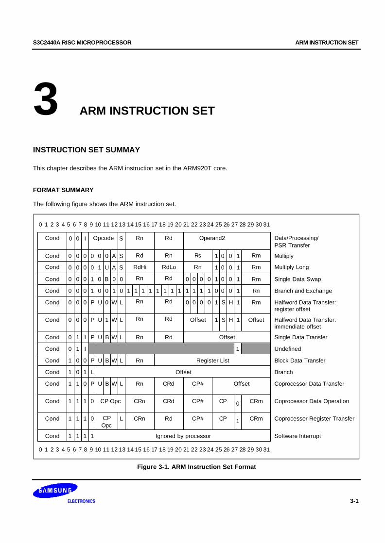
S3C2440A RISC MICROPROCESSOR ARM INSTRUCTION SET
3-1
3 ARM INSTRUCTION SET
INSTRUCTION SET SUMMAY
This chapter describes the ARM instruction set in the ARM920T core.
FORMAT SUMMARY
The following figure shows the ARM instruction set.
Cond Rn Data/Processing/PSR Transfer
0 0 I SOpcode
0 0 0 P U 0 W L
0 0 0 P U 1 W L
0 1 I P U B W L
0 1 I
1 0 0 P U B W L
11 11 1 1 11
1 0 L1
1 1 0 P U B W L
1 1 11
1 1 01
1 1 01 L
Rd
Rd
RnRdHi RdLo
Rn
Rn
Rn
Rn
Rd
Rd
Rd
Rn Register List
Rn
CRn
CRn
CRd
Rd
CP Opc
CPOpc
Operand2
Rs
Rm
Rm
Rm
Rm
Rn
Rn
Rd
Offset Offset
CRd OffsetCP#
CP#
CP#
CP
CP
CRm
CRm
Ignored by processor
0
1
Offset
Cond
Cond
Cond
Cond
Cond
Cond
Cond
Cond
Cond
Cond
Cond
Cond
Cond
Cond
0 0 0 0 00 A S
A SU10 0 00
0 0 0 0 0 01 B
1 00 010 0 0
1
1
1
1
1
1
0
0
0
0
H
H
0
0
0
0
S
S
1
1
1
0
1
1
1
0
0
1
0
0
1
0
0
1
0
0
1
Multiply
Multiply Long
Single Data Swap
Branch and Exchange
Halfword Data Transfer:register offset
Halfword Data Transfer:immendiate offset
Single Data Transfer
Undefined
Block Data Transfer
Branch
Coprocessor Register Transfer
Coprocessor Data Operation
Coprocessor Data Transfer
Software Interrupt
Offset
2726252423222120191817161513 14121110 313029289876543210
2726252423222120191817161513 14121110 313029289876543210
Figure 3-1. ARM Instruction Set Format
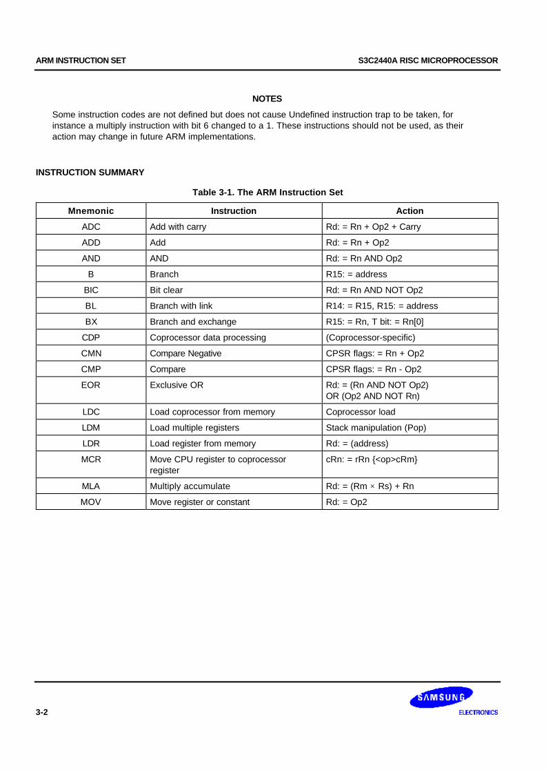
ARM INSTRUCTION SET S3C2440A RISC MICROPROCESSOR
3-2
NOTES
Some instruction codes are not defined but does not cause Undefined instruction trap to be taken, forinstance a multiply instruction with bit 6 changed to a 1. These instructions should not be used, as theiraction may change in future ARM implementations.
INSTRUCTION SUMMARY
Table 3-1. The ARM Instruction Set
Mnemonic Instruction Action
ADC Add with carry Rd: = Rn + Op2 + Carry
ADD Add Rd: = Rn + Op2
AND AND Rd: = Rn AND Op2
B Branch R15: = address
BIC Bit clear Rd: = Rn AND NOT Op2
BL Branch with link R14: = R15, R15: = address
BX Branch and exchange R15: = Rn, T bit: = Rn[0]
CDP Coprocessor data processing (Coprocessor-specific)
CMN Compare Negative CPSR flags: = Rn + Op2
CMP Compare CPSR flags: = Rn - Op2
EOR Exclusive OR Rd: = (Rn AND NOT Op2)OR (Op2 AND NOT Rn)
LDC Load coprocessor from memory Coprocessor load
LDM Load multiple registers Stack manipulation (Pop)
LDR Load register from memory Rd: = (address)
MCR Move CPU register to coprocessorregister
cRn: = rRn <op>cRm
MLA Multiply accumulate Rd: = (Rm × Rs) + Rn
MOV Move register or constant Rd: = Op2
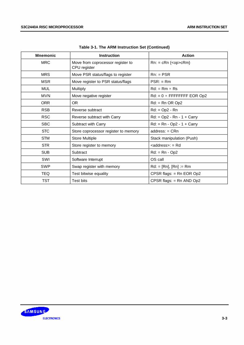
S3C2440A RISC MICROPROCESSOR ARM INSTRUCTION SET
3-3
Table 3-1. The ARM Instruction Set (Continued)
Mnemonic Instruction Action
MRC Move from coprocessor register toCPU register
Rn: = cRn <op>cRm
MRS Move PSR status/flags to register Rn: = PSR
MSR Move register to PSR status/flags PSR: = Rm
MUL Multiply Rd: = Rm × Rs
MVN Move negative register Rd: = 0 × FFFFFFFF EOR Op2
ORR OR Rd: = Rn OR Op2
RSB Reverse subtract Rd: = Op2 - Rn
RSC Reverse subtract with Carry Rd: = Op2 - Rn - 1 + Carry
SBC Subtract with Carry Rd: = Rn - Op2 - 1 + Carry
STC Store coprocessor register to memory address: = CRn
STM Store Multiple Stack manipulation (Push)
STR Store register to memory <address>: = Rd
SUB Subtract Rd: = Rn - Op2
SWI Software Interrupt OS call
SWP Swap register with memory Rd: = [Rn], [Rn] := Rm
TEQ Test bitwise equality CPSR flags: = Rn EOR Op2
TST Test bits CPSR flags: = Rn AND Op2
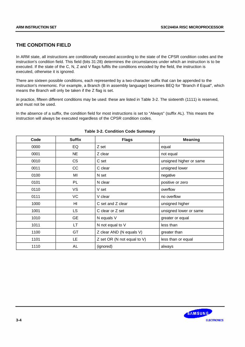
ARM INSTRUCTION SET S3C2440A RISC MICROPROCESSOR
3-4
THE CONDITION FIELD
In ARM state, all instructions are conditionally executed according to the state of the CPSR condition codes and theinstruction's condition field. This field (bits 31:28) determines the circumstances under which an instruction is to beexecuted. If the state of the C, N, Z and V flags fulfils the conditions encoded by the field, the instruction isexecuted, otherwise it is ignored.
There are sixteen possible conditions, each represented by a two-character suffix that can be appended to theinstruction's mnemonic. For example, a Branch (B in assembly language) becomes BEQ for "Branch if Equal", whichmeans the Branch will only be taken if the Z flag is set.
In practice, fifteen different conditions may be used: these are listed in Table 3-2. The sixteenth (1111) is reserved,and must not be used.
In the absence of a suffix, the condition field for most instructions is set to "Always" (suffix AL). This means theinstruction will always be executed regardless of the CPSR condition codes.
Table 3-2. Condition Code Summary
Code Suffix Flags Meaning
0000 EQ Z set equal
0001 NE Z clear not equal
0010 CS C set unsigned higher or same
0011 CC C clear unsigned lower
0100 MI N set negative
0101 PL N clear positive or zero
0110 VS V set overflow
0111 VC V clear no overflow
1000 HI C set and Z clear unsigned higher
1001 LS C clear or Z set unsigned lower or same
1010 GE N equals V greater or equal
1011 LT N not equal to V less than
1100 GT Z clear AND (N equals V) greater than
1101 LE Z set OR (N not equal to V) less than or equal
1110 AL (ignored) always
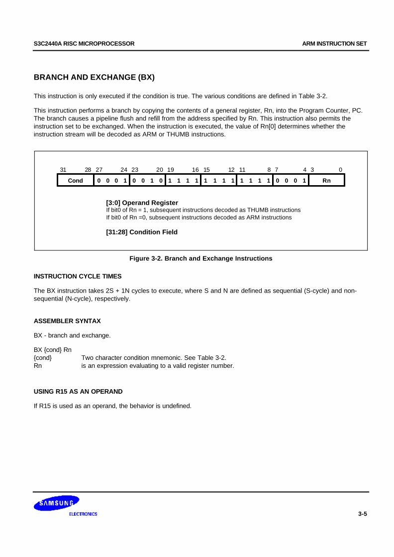
S3C2440A RISC MICROPROCESSOR ARM INSTRUCTION SET
3-5
BRANCH AND EXCHANGE (BX)
This instruction is only executed if the condition is true. The various conditions are defined in Table 3-2.
This instruction performs a branch by copying the contents of a general register, Rn, into the Program Counter, PC.The branch causes a pipeline flush and refill from the address specified by Rn. This instruction also permits theinstruction set to be exchanged. When the instruction is executed, the value of Rn[0] determines whether theinstruction stream will be decoded as ARM or THUMB instructions.
31 2427 19 15 8 7 0
00 0 1 10 0 0 11 1 1 11 1 1 11 1 1 00 0 1Cond Rn
28 16 111223 20 4 3
[3:0] Operand RegisterIf bit0 of Rn = 1, subsequent instructions decoded as THUMB instructionsIf bit0 of Rn =0, subsequent instructions decoded as ARM instructions
[31:28] Condition Field
Figure 3-2. Branch and Exchange Instructions
INSTRUCTION CYCLE TIMES
The BX instruction takes 2S + 1N cycles to execute, where S and N are defined as sequential (S-cycle) and non-sequential (N-cycle), respectively.
ASSEMBLER SYNTAX
BX - branch and exchange.
BX cond Rncond Two character condition mnemonic. See Table 3-2.Rn is an expression evaluating to a valid register number.
USING R15 AS AN OPERAND
If R15 is used as an operand, the behavior is undefined.
ARM INSTRUCTION SET S3C2440A RISC MICROPROCESSOR
3-6
Examples
ADR R0, Into_THUMB + 1 Generate branch target address and set bit 0 high – hence it comes inTHUMB state
BX R0 Branch and change to THUMB state.
CODE16 Assemble subsequent code as
Into_THUMB THUMB instructions
ADR R5, Back_to_ARM Generate branch target to word aligned addresshence bit 0 is low and so change back to ARM state.
BX R5 Branch and change back to ARM state.
ALIGN Word alignment
CODE32 Assemble subsequent code as ARM instructions
Back_to_ARM –

S3C2440A RISC MICROPROCESSOR ARM INSTRUCTION SET
3-7
BRANCH AND BRANCH WITH LINK (B, BL)
The instruction is only executed if the condition is true. The various conditions are defined Table 3-2. The instructionencoding is shown in Figure 3-3, below.
31 2427
Cond Offset
28 23
[24] Link bit0 = Branch 1 = Branch with link
[31:28] Condition Field
25
101 L
0
Figure 3-3. Branch Instructions
Branch instruction contains a signed 2's complement 24 bit offset. This is shifted left two bits, sign extended to 32bits, and added to the PC. The instruction can therefore specify a branch of +/- 32Mbytes. The branch offset musttake account of the prefetch operation, which causes the PC to be 2 words (8 bytes) ahead of the current instruction.
Branches beyond +/- 32Mbytes must use an offset or absolute destination which has been previously loaded into aregister. In this case the PC should be manually saved in R14 if a Branch with Link type operation is required.
THE LINK BIT
Branch with Link (BL) writes the old PC into the link register (R14) of the current bank. The PC value written into R14is adjusted to allow for the prefetch, and contains the address of the instruction following the branch and linkinstruction. Note that the CPSR is not saved with the PC and R14[1:0] are always cleared.
To return from a routine called by Branch with Link use MOV PC,R14 if the link register is still valid or LDMRn!,..PC if the link register has been saved onto a stack pointed to by Rn.
INSTRUCTION CYCLE TIMES
Branch and Branch with Link instructions take 2S + 1N incremental cycles, where S and N are defined as sequential(S-cycle) and internal (I-cycle).
ARM INSTRUCTION SET S3C2440A RISC MICROPROCESSOR
3-8
ASSEMBLER SYNTAX
Items in “” are optional. Items in “<>” must be present.
BLcond <expression>
L Used to request the Branch with Link form of the instruction.
If absent, R14 will not be affected by the instruction.
cond A two-character mnemonic as shown in Table 3-2.
If absent then AL (ALways) will be used.
<expression> The destination. The assembler calculates the offset
Examples
here BAL here ; Assembles to 0xEAFFFFFE (note effect of PC offset).B there ; Always condition used as default.CMP R1,#0 ; Compare R1 with zero and branch to fred
if R1 was zero, otherwise continue.BEQ fred ; Continue to next instruction.BL sub+ROM ; Call subroutine at computed address.ADDS R1,#1 ; Add 1 to register 1, setting CPSR flags
on the result then call subroutine ifBLCC sub ; the C flag is clear, which will be the
case unless R1 held 0xFFFFFFFF.
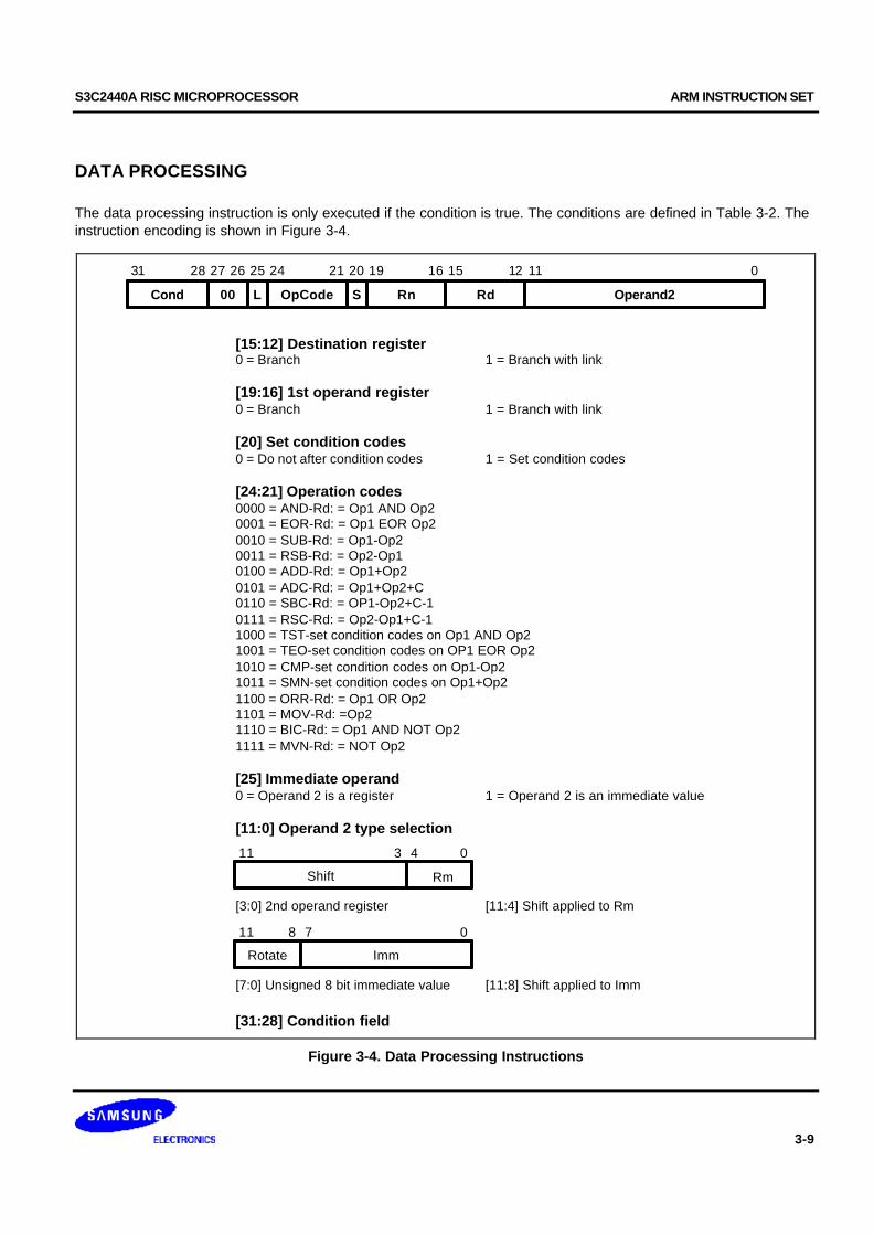
S3C2440A RISC MICROPROCESSOR ARM INSTRUCTION SET
3-9
DATA PROCESSING
The data processing instruction is only executed if the condition is true. The conditions are defined in Table 3-2. Theinstruction encoding is shown in Figure 3-4.
31 2427 19 15
Cond Operand2
28 16 111221
[15:12] Destination register0 = Branch 1 = Branch with link
[19:16] 1st operand register0 = Branch 1 = Branch with link
[20] Set condition codes0 = Do not after condition codes 1 = Set condition codes
[24:21] Operation codes0000 = AND-Rd: = Op1 AND Op20001 = EOR-Rd: = Op1 EOR Op20010 = SUB-Rd: = Op1-Op20011 = RSB-Rd: = Op2-Op10100 = ADD-Rd: = Op1+Op20101 = ADC-Rd: = Op1+Op2+C0110 = SBC-Rd: = OP1-Op2+C-10111 = RSC-Rd: = Op2-Op1+C-11000 = TST-set condition codes on Op1 AND Op21001 = TEO-set condition codes on OP1 EOR Op21010 = CMP-set condition codes on Op1-Op21011 = SMN-set condition codes on Op1+Op21100 = ORR-Rd: = Op1 OR Op21101 = MOV-Rd: =Op21110 = BIC-Rd: = Op1 AND NOT Op21111 = MVN-Rd: = NOT Op2
[25] Immediate operand0 = Operand 2 is a register 1 = Operand 2 is an immediate value
[11:0] Operand 2 type selection
26 25
00 L
20
OpCode S Rn Rd
0
Rotate
Shift Rm
[3:0] 2nd operand register [11:4] Shift applied to Rm
311 04
811 07
Imm
[7:0] Unsigned 8 bit immediate value [11:8] Shift applied to Imm
[31:28] Condition field
Figure 3-4. Data Processing Instructions
ARM INSTRUCTION SET S3C2440A RISC MICROPROCESSOR
3-10
The instruction produces a result by performing a specified arithmetic or logical operation on one or two operands.The first operand is always a register (Rn).
The second operand may be a shifted register (Rm) or a rotated 8 bit immediate value (Imm) according to the value ofthe I bit in the instruction. The condition codes in the CPSR may be preserved or updated as a result of thisinstruction, according to the value of the S bit in the instruction.
Certain operations (TST, TEQ, CMP, CMN) do not write the result to Rd. They are used only to perform tests and toset the condition codes on the result and always have the S bit set. The instructions and their effects are listed inTable 3-3.
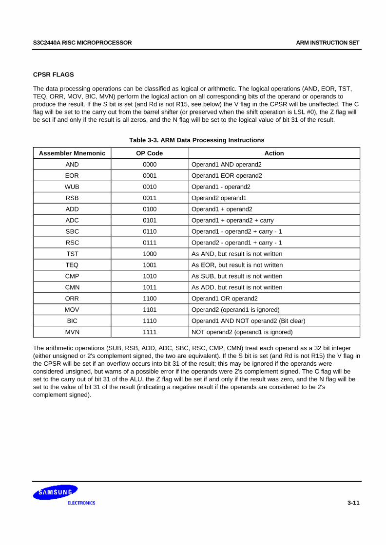
S3C2440A RISC MICROPROCESSOR ARM INSTRUCTION SET
3-11
CPSR FLAGS
The data processing operations can be classified as logical or arithmetic. The logical operations (AND, EOR, TST,TEQ, ORR, MOV, BIC, MVN) perform the logical action on all corresponding bits of the operand or operands toproduce the result. If the S bit is set (and Rd is not R15, see below) the V flag in the CPSR will be unaffected. The Cflag will be set to the carry out from the barrel shifter (or preserved when the shift operation is LSL #0), the Z flag willbe set if and only if the result is all zeros, and the N flag will be set to the logical value of bit 31 of the result.
Table 3-3. ARM Data Processing Instructions
Assembler Mnemonic OP Code Action
AND 0000 Operand1 AND operand2
EOR 0001 Operand1 EOR operand2
WUB 0010 Operand1 - operand2
RSB 0011 Operand2 operand1
ADD 0100 Operand1 + operand2
ADC 0101 Operand1 + operand2 + carry
SBC 0110 Operand1 - operand2 + carry - 1
RSC 0111 Operand2 - operand1 + carry - 1
TST 1000 As AND, but result is not written
TEQ 1001 As EOR, but result is not written
CMP 1010 As SUB, but result is not written
CMN 1011 As ADD, but result is not written
ORR 1100 Operand1 OR operand2
MOV 1101 Operand2 (operand1 is ignored)
BIC 1110 Operand1 AND NOT operand2 (Bit clear)
MVN 1111 NOT operand2 (operand1 is ignored)
The arithmetic operations (SUB, RSB, ADD, ADC, SBC, RSC, CMP, CMN) treat each operand as a 32 bit integer(either unsigned or 2's complement signed, the two are equivalent). If the S bit is set (and Rd is not R15) the V flag inthe CPSR will be set if an overflow occurs into bit 31 of the result; this may be ignored if the operands wereconsidered unsigned, but warns of a possible error if the operands were 2's complement signed. The C flag will beset to the carry out of bit 31 of the ALU, the Z flag will be set if and only if the result was zero, and the N flag will beset to the value of bit 31 of the result (indicating a negative result if the operands are considered to be 2'scomplement signed).
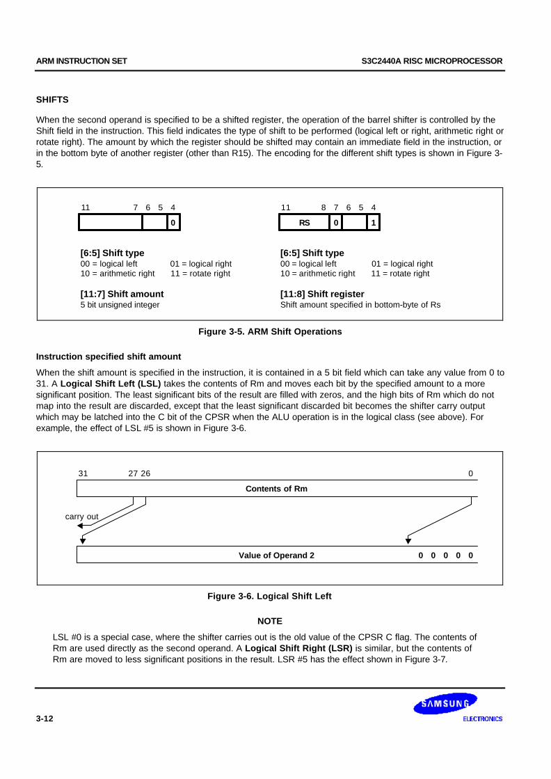
ARM INSTRUCTION SET S3C2440A RISC MICROPROCESSOR
3-12
SHIFTS
When the second operand is specified to be a shifted register, the operation of the barrel shifter is controlled by theShift field in the instruction. This field indicates the type of shift to be performed (logical left or right, arithmetic right orrotate right). The amount by which the register should be shifted may contain an immediate field in the instruction, orin the bottom byte of another register (other than R15). The encoding for the different shift types is shown in Figure 3-5.
0
[6:5] Shift type00 = logical left 01 = logical right10 = arithmetic right 11 = rotate right
[11:7] Shift amount5 bit unsigned integer
[6:5] Shift type00 = logical left 01 = logical right10 = arithmetic right 11 = rotate right
[11:8] Shift registerShift amount specified in bottom-byte of Rs
456711
1
456711 8
0RS
Figure 3-5. ARM Shift Operations
Instruction specified shift amount
When the shift amount is specified in the instruction, it is contained in a 5 bit field which can take any value from 0 to31. A Logical Shift Left (LSL) takes the contents of Rm and moves each bit by the specified amount to a moresignificant position. The least significant bits of the result are filled with zeros, and the high bits of Rm which do notmap into the result are discarded, except that the least significant discarded bit becomes the shifter carry outputwhich may be latched into the C bit of the CPSR when the ALU operation is in the logical class (see above). Forexample, the effect of LSL #5 is shown in Figure 3-6.
31 27 26
Contents of Rm
Value of Operand 2
carry out
0
0
0000
Figure 3-6. Logical Shift Left
NOTE
LSL #0 is a special case, where the shifter carries out is the old value of the CPSR C flag. The contents ofRm are used directly as the second operand. A Logical Shift Right (LSR) is similar, but the contents ofRm are moved to less significant positions in the result. LSR #5 has the effect shown in Figure 3-7.
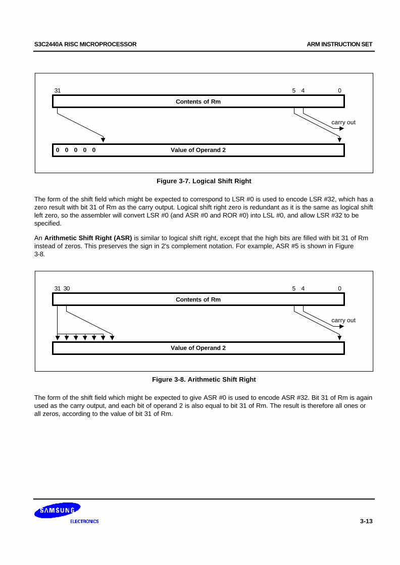
S3C2440A RISC MICROPROCESSOR ARM INSTRUCTION SET
3-13
31
Contents of Rm
Value of Operand 2
0
carry out
45
00000
Figure 3-7. Logical Shift Right
The form of the shift field which might be expected to correspond to LSR #0 is used to encode LSR #32, which has azero result with bit 31 of Rm as the carry output. Logical shift right zero is redundant as it is the same as logical shiftleft zero, so the assembler will convert LSR #0 (and ASR #0 and ROR #0) into LSL #0, and allow LSR #32 to bespecified.
An Arithmetic Shift Right (ASR) is similar to logical shift right, except that the high bits are filled with bit 31 of Rminstead of zeros. This preserves the sign in 2's complement notation. For example, ASR #5 is shown in Figure3-8.
31
Contents of Rm
Value of Operand 2
0
carry out
4530
Figure 3-8. Arithmetic Shift Right
The form of the shift field which might be expected to give ASR #0 is used to encode ASR #32. Bit 31 of Rm is againused as the carry output, and each bit of operand 2 is also equal to bit 31 of Rm. The result is therefore all ones orall zeros, according to the value of bit 31 of Rm.
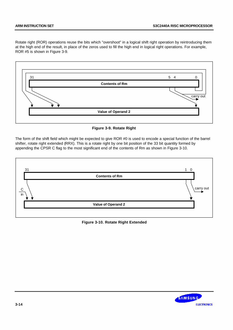
ARM INSTRUCTION SET S3C2440A RISC MICROPROCESSOR
3-14
Rotate right (ROR) operations reuse the bits which "overshoot" in a logical shift right operation by reintroducing themat the high end of the result, in place of the zeros used to fill the high end in logical right operations. For example,ROR #5 is shown in Figure 3-9.
31
Contents of Rm
Value of Operand 2
0
carry out
45
Figure 3-9. Rotate Right
The form of the shift field which might be expected to give ROR #0 is used to encode a special function of the barrelshifter, rotate right extended (RRX). This is a rotate right by one bit position of the 33 bit quantity formed byappending the CPSR C flag to the most significant end of the contents of Rm as shown in Figure 3-10.
31
Contents of Rm
Value of Operand 2
01
carry outCin
Figure 3-10. Rotate Right Extended
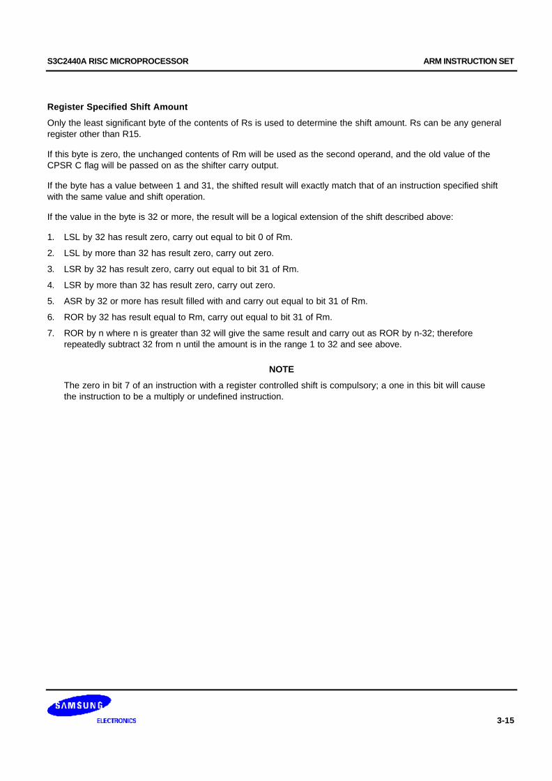
S3C2440A RISC MICROPROCESSOR ARM INSTRUCTION SET
3-15
Register Specified Shift Amount
Only the least significant byte of the contents of Rs is used to determine the shift amount. Rs can be any generalregister other than R15.
If this byte is zero, the unchanged contents of Rm will be used as the second operand, and the old value of theCPSR C flag will be passed on as the shifter carry output.
If the byte has a value between 1 and 31, the shifted result will exactly match that of an instruction specified shiftwith the same value and shift operation.
If the value in the byte is 32 or more, the result will be a logical extension of the shift described above:
1. LSL by 32 has result zero, carry out equal to bit 0 of Rm.
2. LSL by more than 32 has result zero, carry out zero.
3. LSR by 32 has result zero, carry out equal to bit 31 of Rm.
4. LSR by more than 32 has result zero, carry out zero.
5. ASR by 32 or more has result filled with and carry out equal to bit 31 of Rm.
6. ROR by 32 has result equal to Rm, carry out equal to bit 31 of Rm.
7. ROR by n where n is greater than 32 will give the same result and carry out as ROR by n-32; thereforerepeatedly subtract 32 from n until the amount is in the range 1 to 32 and see above.
NOTE
The zero in bit 7 of an instruction with a register controlled shift is compulsory; a one in this bit will causethe instruction to be a multiply or undefined instruction.
ARM INSTRUCTION SET S3C2440A RISC MICROPROCESSOR
3-16
IMMEDIATE OPERAND ROTATES
The immediate operand rotate field is a 4 bit unsigned integer which specifies a shift operation on the 8 bit immediatevalue. This value is zero extended to 32 bits, and then subject to a rotate right by twice the value in the rotate field.This enables many common constants to be generated, for example all powers of 2.
WRITING TO R15
When Rd is a register other than R15, the condition code flags in the CPSR may be updated from the ALU flags asdescribed above.
When Rd is R15 and the S flag in the instruction is not set the result of the operation is placed in R15 and the CPSRis unaffected.
When Rd is R15 and the S flag is set the result of the operation is placed in R15 and the SPSR corresponding to thecurrent mode is moved to the CPSR. This allows state changes which automatically restore both PC and CPSR.This form of instruction should not be used in User mode.
USING R15 AS AN OPERANDY
If R15 (the PC) is used as an operand in a data processing instruction the register is used directly.
The PC value will be the address of the instruction, plus 8 or 12 bytes due to instruction prefetching. If the shiftamount is specified in the instruction, the PC will be 8 bytes ahead. If a register is used to specify the shift amountthe PC will be 12 bytes ahead.
TEQ, TST, CMP AND CMN OPCODES
NOTE
TEQ, TST, CMP and CMN do not write the result of their operation but do set flags in the CPSR. Anassembler should always set the S flag for these instructions even if this is not specified in the mnemonic.
The TEQP form of the TEQ instruction used in earlier ARM processors must not be used: the PSR transferoperations should be used instead.
The action of TEQP in the ARM920T is to move SPSR_<mode> to the CPSR if the processor is in a privileged modeand to do nothing if in User mode.
INSTRUCTION CYCLE TIMES
Data Processing instructions vary in the number of incremental cycles taken as follows:
Table 3-4. Incremental Cycle Times
Processing Type Cycles
Normal data processing 1S
Data processing with register specified shift 1S + 1I
Data processing with PC written 2S + 1N
Data processing with register specified shift and PC written 2S + 1N +1I
NOTE: S, N and I are as defined sequential (S-cycle), non-sequential (N-cycle), and internal (I-cycle) respectively.

S3C2440A RISC MICROPROCESSOR ARM INSTRUCTION SET
3-17
ASSEMBLER SYNTAX
• MOV,MVN (single operand instructions).<opcode>condS Rd,<Op2>
• CMP,CMN,TEQ,TST (instructions which do not produce a result).<opcode>cond Rn,<Op2>
• AND,EOR,SUB,RSB,ADD,ADC,SBC,RSC,ORR,BIC<opcode>condS Rd,Rn,<Op2>
where:
<Op2> Rm,<shift> or,<#expression>
cond A two-character condition mnemonic. See Table 3-2.
S Set condition codes if S present (implied for CMP, CMN, TEQ, TST).
Rd, Rn and Rm Expressions evaluating to a register number.
<#expression> If this is used, the assembler will attempt to generate a shifted immediate 8-bit field tomatch the expression. If this is impossible, it will give an error.
<shift> <Shiftname> <register> or <shiftname> #expression, or RRX (rotate right one bit withextend).
<shiftname>s ASL, LSL, LSR, ASR, ROR. (ASL is a synonym for LSL, they assemble to the samecode.)
EXAMPLES
ADDEQ R2,R4,R5 ; If the Z flag is set make R2:=R4+R5TEQS R4,#3 ; Test R4 for equality with 3.
; (The S is in fact redundant as the; assembler inserts it automatically.)
SUB R4,R5,R7,LSR R2 ; Logical right shift R7 by the number in; the bottom byte of R2, subtract result; from R5, and put the answer into R4.
MOV PC,R14 ; Return from subroutine.MOVS PC,R14 ; Return from exception and restore CPSR
; from SPSR_mode.
ARM INSTRUCTION SET S3C2440A RISC MICROPROCESSOR
3-18
PSR TRANSFER (MRS, MSR)
The instruction is only executed if the condition is true. The various conditions are defined in Table 3-2.
The MRS and MSR instructions are formed from a subset of the Data Processing operations and are implementedusing the TEQ, TST, CMN and CMP instructions without the S flag set. The encoding is shown in Figure 3-11.
These instructions allow access to the CPSR and SPSR registers. The MRS instruction allows the contents of theCPSR or SPSR_<mode> to be moved to a general register. The MSR instruction allows the contents of a generalregister to be moved to the CPSR or SPSR_<mode> register.
The MSR instruction also allows an immediate value or register contents to be transferred to the condition code flags(N,Z,C and V) of CPSR or SPSR_<mode> without affecting the control bits. In this case, the top four bits of thespecified register contents or 32 bit immediate value are written to the top four bits of the relevant PSR.
OPERAND RESTRICTIONS
• In user mode, the control bits of the CPSR are protected from change, so only the condition code flags of theCPSR can be changed. In other (privileged) modes the entire CPSR can be changed.
• Note that the software must never change the state of the T bit in the CPSR. If this happens, the processor willenter an unpredictable state.
• The SPSR register which is accessed depends on the mode at the time of execution. For example, onlySPSR_fiq is accessible when the processor is in FIQ mode.
• You must not specify R15 as the source or destination register.
• Also, do not attempt to access an SPSR in User mode, since no such register exists.
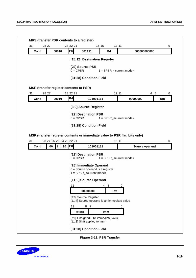
S3C2440A RISC MICROPROCESSOR ARM INSTRUCTION SET
3-19
MSR (transfer register contents or immediate value to PSR flag bits only)
Cond Source operandPd 101001111
31 222728 11122123
I 1000
26 25 24 0
Cond 0000000000010 Pd 101001111
31 222728 11122123
Rm
MSR (transfer register contents to PSR)
4 3 0
Cond 00000000000000010 RdPs 001111
31 2227 1528 16 11122123
MRS (transfer PSR contents to a register)
0
[3:0] Source Register
[22] Destination PSR0 = CPSR 1 = SPSR_<current mode>
[31:28] Condition Field
[15:12] Destination Register
[22] Source PSR0 = CPSR 1 = SPSR_<current mode>
[31:28] Condition Field
[3:0] Source Register[11:4] Source operand is an immediate value
[7:0] Unsigned 8 bit immediate value[11:8] Shift applied to Imm
[22] Destination PSR0 = CPSR 1 = SPSR_<current mode>
[25] Immediate Operand0 = Source operand is a register1 = SPSR_<current mode>
[11:0] Source Operand
[31:28] Condition Field
00000000 Rm
11 4 3 0
Rotate Imm
11 08 7
Figure 3-11. PSR Transfer
ARM INSTRUCTION SET S3C2440A RISC MICROPROCESSOR
3-20
RESERVED BITS
Only twelve bits of the PSR are defined in ARM920T (N,Z,C,V,I,F, T & M[4:0]); the remaining bits are reserved for usein future versions of the processor. Refer to Figure 2-6 for a full description of the PSR bits.
To ensure the maximum compatibility between ARM920T programs and future processors, the following rules shouldbe observed:
• The reserved bits should be preserved while changing the value in a PSR.
• Programs should not rely on specific values from the reserved bits while checking the PSR status, since theymay read as one or zero in future processors.
A read-modify-write strategy should therefore be used when altering the control bits of any PSR register; this involvestransferring the appropriate PSR register to a general register using the MRS instruction, changing only the relevantbits and then transferring the modified value back to the PSR register using the MSR instruction.
EXAMPLES
The following sequence performs a mode change:
MRS R0,CPSR ; Take a copy of the CPSR.BIC R0,R0,#0x1F ; Clear the mode bits.ORR R0,R0,#new_mode ; Select new modeMSR CPSR,R0 ; Write back the modified CPSR.
When the aim is simply to change the condition code flags in a PSR, a value can be written directly to the flag bitswithout disturbing the control bits. The following instruction sets the N,Z,C and V flags:
MSR CPSR_flg,#0xF0000000 ; Set all the flags regardless of their previous state; (does not affect any control bits).
No attempt should be made to write an 8 bit immediate value into the whole PSR since such an operation cannotpreserve the reserved bits.
INSTRUCTION CYCLE TIMES
PSR transfers take 1S incremental cycles, where S is defined as Sequential (S-cycle).
S3C2440A RISC MICROPROCESSOR ARM INSTRUCTION SET
3-21
ASSEMBLY SYNTAX
• MRS - transfer PSR contents to a registerMRScond Rd,<psr>
• MSR - transfer register contents to PSRMSRcond <psr>,Rm
• MSR - transfer register contents to PSR flag bits onlyMSRcond <psrf>,Rm
The most significant four bits of the register contents are written to the N,Z,C & V flags respectively.
• MSR - transfer immediate value to PSR flag bits onlyMSRcond <psrf>,<#expression>
The expression should symbolise a 32 bit value of which the most significant four bits are written to the N,Z,C and Vflags respectively.
Key:
cond Two-character condition mnemonic. See Table 3-2..
Rd and Rm Expressions evaluating to a register number other than R15
<psr> CPSR, CPSR_all, SPSR or SPSR_all. (CPSR and CPSR_all are synonyms as are SPSRand SPSR_all)
<psrf> CPSR_flg or SPSR_flg
<#expression> Where this is used, the assembler will attempt to generate a shifted immediate 8-bit fieldto match the expression. If this is impossible, it will give an error.
EXAMPLES
In User mode the instructions behave as follows:
MSR CPSR_all,Rm ; CPSR[31:28] <- Rm[31:28]MSR CPSR_flg,Rm ; CPSR[31:28] <- Rm[31:28]MSR CPSR_flg,#0xA0000000 ; CPSR[31:28] <- 0xA (set N,C; clear Z,V)MRS Rd,CPSR ; Rd[31:0] <- CPSR[31:0]
In privileged modes the instructions behave as follows:
MSR CPSR_all,Rm ; CPSR[31:0] <- Rm[31:0]MSR CPSR_flg,Rm ; CPSR[31:28] <- Rm[31:28]MSR CPSR_flg,#0x50000000 ; CPSR[31:28] <- 0x5 (set Z,V; clear N,C)MSR SPSR_all,Rm ; SPSR_<mode>[31:0]<- Rm[31:0]MSR SPSR_flg,Rm ; SPSR_<mode>[31:28] <- Rm[31:28]MSR SPSR_flg,#0xC0000000 ; SPSR_<mode>[31:28] <- 0xC (set N,Z; clear C,V)MRS Rd,SPSR ; Rd[31:0] <- SPSR_<mode>[31:0]

ARM INSTRUCTION SET S3C2440A RISC MICROPROCESSOR
3-22
MULTIPLY AND MULTIPLY-ACCUMULATE (MUL, MLA)
The instruction is only executed if the condition is true. The various conditions are defined in Table 3-2. Theinstruction encoding is shown in Figure 3-12.
The multiply and multiply-accumulate instructions use an 8 bit Booth's algorithm to perform integer multiplication.
31 27 19 15
Cond
28 16 111221 20
S Rd Rn
[15:12][11:8][3:0] Operand Registers[19:16] Destination Register
[20] Set Condition Code0 = Do not after condition codes1 = Set condition codes
[21] Accumulate0 = Multiply only1 = Multiply and accumulate
[31:28] Condition Field
22
1 0 0 1Rs RmA00 0 0 0 0
8 7 4 3 0
Figure 3-12. Multiply Instructions
The multiply form of the instruction gives Rd:=Rm*Rs. Rn is ignored, and should be set to zero for compatibility withpossible future upgrades to the instruction set. The multiply-accumulate form gives Rd:=Rm*Rs+Rn, which can savean explicit ADD instruction in some circumstances. Both forms of the instruction work on operands which may beconsidered as signed (2's complement) or unsigned integers.
The results of a signed multiply and of an unsigned multiply of 32 bit operands differ only in the upper 32 bits - thelow 32 bits of the signed and unsigned results are identical. As these instructions only produce the low 32 bits of amultiply, they can be used for both signed and unsigned multiplies.
For example consider the multiplication of the operands:Operand A Operand B Result0xFFFFFFF6 0x0000001 0xFFFFFF38
S3C2440A RISC MICROPROCESSOR ARM INSTRUCTION SET
3-23
If the Operands Are Interpreted as Signed
Operand A has the value -10, operand B has the value 20, and the result is -200 which is correctly represented as0xFFFFFF38.
If the Operands Are Interpreted as Unsigned
Operand A has the value 4294967286, operand B has the value 20 and the result is 85899345720, which isrepresented as 0x13FFFFFF38, so the least significant 32 bits are 0xFFFFFF38.
Operand Restrictions
The destination register Rd must not be the same as the operand register Rm. R15 must not be used as an operandor as the destination register.
All other register combinations will give correct results, and Rd, Rn and Rs may use the same register whenrequired.
ARM INSTRUCTION SET S3C2440A RISC MICROPROCESSOR
3-24
CPSR FLAGS
Setting the CPSR flags is optional, and is controlled by the S bit in the instruction. The N (Negative) and Z (Zero)flags are set correctly on the result (N is made equal to bit 31 of the result, and Z is set if and only if the result iszero). The C (Carry) flag is set to a meaningless value and the V (oVerflow) flag is unaffected.
INSTRUCTION CYCLE TIMES
MUL takes 1S + mI and MLA 1S + (m+1)I cycles to execute, where S and I are defined as sequential (S-cycle) andinternal (I-cycle), respectively.
m The number of 8 bit multiplier array cycles is required to complete the multiply, which iscontrolled by the value of the multiplier operand specified by Rs. Its possible values are as follows
1 If bits [32:8] of the multiplier operand are all zero or all one.
2 If bits [32:16] of the multiplier operand are all zero or all one.
3 If bits [32:24] of the multiplier operand are all zero or all one.
4 In all other cases.
ASSEMBLER SYNTAX
MULcondS Rd,Rm,RsMLAcondS Rd,Rm,Rs,Rn
cond Two-character condition mnemonic. See Table 3-2..
S Set condition codes if S present
Rd, Rm, Rs and Rn Expressions evaluating to a register number other than R15.
EXAMPLES
MUL R1,R2,R3 ; R1:=R2*R3MLAEQS R1,R2,R3,R4 ; Conditionally R1:=R2*R3+R4, Setting condition codes.
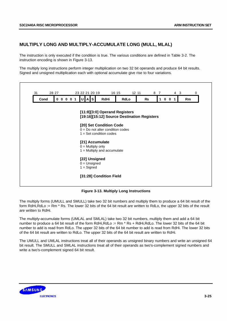
S3C2440A RISC MICROPROCESSOR ARM INSTRUCTION SET
3-25
MULTIPLY LONG AND MULTIPLY-ACCUMULATE LONG (MULL, MLAL)
The instruction is only executed if the condition is true. The various conditions are defined in Table 3-2. Theinstruction encoding is shown in Figure 3-13.
The multiply long instructions perform integer multiplication on two 32 bit operands and produce 64 bit results.Signed and unsigned multiplication each with optional accumulate give rise to four variations.
31 27 19 15
Cond
28 16 11122123
U
20
S RdHi RdLo
[11:8][3:0] Operand Registers[19:16][15:12] Source Destination Registers
[20] Set Condition Code0 = Do not alter condition codes1 = Set condition codes
[21] Accumulate0 = Multiply only1 = Multiply and accumulate
[22] Unsigned0 = Unsigned1 = Signed
[31:28] Condition Field
22
00 0 0 1 1 0 0 1Rs RmA
8 7 4 3 0
Figure 3-13. Multiply Long Instructions
The multiply forms (UMULL and SMULL) take two 32 bit numbers and multiply them to produce a 64 bit result of theform RdHi,RdLo := Rm * Rs. The lower 32 bits of the 64 bit result are written to RdLo, the upper 32 bits of the resultare written to RdHi.
The multiply-accumulate forms (UMLAL and SMLAL) take two 32 bit numbers, multiply them and add a 64 bitnumber to produce a 64 bit result of the form RdHi,RdLo := Rm * Rs + RdHi,RdLo. The lower 32 bits of the 64 bitnumber to add is read from RdLo. The upper 32 bits of the 64 bit number to add is read from RdHi. The lower 32 bitsof the 64 bit result are written to RdLo. The upper 32 bits of the 64 bit result are written to RdHi.
The UMULL and UMLAL instructions treat all of their operands as unsigned binary numbers and write an unsigned 64bit result. The SMULL and SMLAL instructions treat all of their operands as two's-complement signed numbers andwrite a two's-complement signed 64 bit result.
ARM INSTRUCTION SET S3C2440A RISC MICROPROCESSOR
3-26
OPERAND RESTRICTIONS
• R15 must not be used as an operand or as a destination register.
• RdHi, RdLo, and Rm must all specify different registers.
CPSR FLAGS
Setting the CPSR flags is optional, and is controlled by the S bit in the instruction. The N and Z flags are setcorrectly on the result (N is equal to bit 63 of the result, Z is set if and only if all 64 bits of the result are zero). Boththe C and V flags are set to meaningless values.
INSTRUCTION CYCLE TIMES
MULL takes 1S + (m+1)I and MLAL 1S + (m+2)I cycles to execute, where m is the number of 8 bit multiplier arraycycles required to complete the multiply, which is controlled by the value of the multiplier operand specified by Rs.
Its possible values are as follows:
For Signed INSTRUCTIONS SMULL, SMLAL:
• If bits [31:8] of the multiplier operand are all zero or all one.
• If bits [31:16] of the multiplier operand are all zero or all one.
• If bits [31:24] of the multiplier operand are all zero or all one.
• In all other cases.
For Unsigned Instructions UMULL, UMLAL:
• If bits [31:8] of the multiplier operand are all zero.
• If bits [31:16] of the multiplier operand are all zero.
• If bits [31:24] of the multiplier operand are all zero.
• In all other cases.
S and I are defined as sequential (S-cycle) and internal (I-cycle), respectively.

S3C2440A RISC MICROPROCESSOR ARM INSTRUCTION SET
3-27
ASSEMBLER SYNTAX
Table 3-5. Assembler Syntax Descriptions
Mnemonic Description Purpose
UMULLcondS RdLo,RdHi,Rm,Rs Unsigned Multiply Long 32 x 32 = 64
UMLALcondS RdLo,RdHi,Rm,Rs Unsigned Multiply & Accumulate Long 32 x 32 + 64 = 64
SMULLcondS RdLo,RdHi,Rm,Rs Signed Multiply Long 32 x 32 = 64
SMLALcondS RdLo,RdHi,Rm,Rs Signed Multiply & Accumulate Long 32 x 32 + 64 = 64
where:
cond Two-character condition mnemonic. See Table 3-2.
S Set condition codes if S present
RdLo, RdHi, Rm, Rs Expressions evaluating to a register number other than R15.
EXAMPLES
UMULL R1,R4,R2,R3 ; R4,R1:=R2*R3UMLALS R1,R5,R2,R3 ; R5,R1:=R2*R3+R5,R1 also setting condition codes
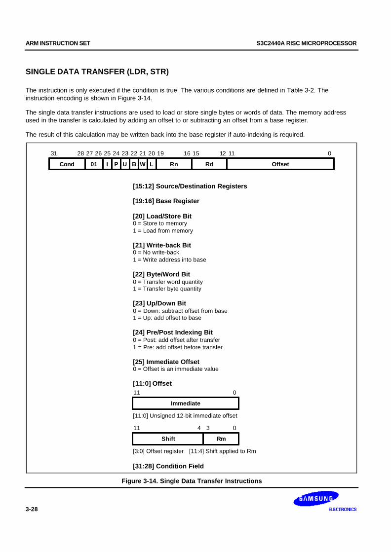
ARM INSTRUCTION SET S3C2440A RISC MICROPROCESSOR
3-28
SINGLE DATA TRANSFER (LDR, STR)
The instruction is only executed if the condition is true. The various conditions are defined in Table 3-2. Theinstruction encoding is shown in Figure 3-14.
The single data transfer instructions are used to load or store single bytes or words of data. The memory addressused in the transfer is calculated by adding an offset to or subtracting an offset from a base register.
The result of this calculation may be written back into the base register if auto-indexing is required.
31 27 19 15 0
Cond
28 16 11122123
B
20
L Rn Rd
22
01 I P U OffsetW
26 2425
[15:12] Source/Destination Registers
[19:16] Base Register
[20] Load/Store Bit0 = Store to memory1 = Load from memory
[21] Write-back Bit0 = No write-back1 = Write address into base
[22] Byte/Word Bit0 = Transfer word quantity1 = Transfer byte quantity
[23] Up/Down Bit0 = Down: subtract offset from base1 = Up: add offset to base
[24] Pre/Post Indexing Bit0 = Post: add offset after transfer1 = Pre: add offset before transfer
[25] Immediate Offset0 = Offset is an immediate value
[11:0] Offset
Shift
Immediate
[11:0] Unsigned 12-bit immediate offset
11
11
Rm
[3:0] Offset register [11:4] Shift applied to Rm
[31:28] Condition Field
0
4 3 0
Figure 3-14. Single Data Transfer Instructions
S3C2440A RISC MICROPROCESSOR ARM INSTRUCTION SET
3-29
OFFSETS AND AUTO-INDEXING
The offset from the base may be either a 12 bit unsigned binary immediate value in the instruction, or a secondregister (possibly shifted in some way). The offset may be added to (U=1) or subtracted from (U=0) the base registerRn. The offset modification may be performed either before (pre-indexed, P=1) or after (post-indexed, P=0) the baseis used as the transfer address.
The W bit gives optional auto increment and decrement addressing modes. The modified base value may be writtenback into the base (W=1), or the old base value may be kept (W=0). In the case of post-indexed addressing, thewrite back bit is redundant and is always set to zero, since the old base value can be retained by setting the offset tozero. Therefore post-indexed data transfers always write back the modified base. The only use of the W bit in a post-indexed data transfer is in privileged mode code, where setting the W bit forces non-privileged mode for the transfer,allowing the operating system to generate a user address in a system where the memory management hardwaremakes suitable use of this hardware.
SHIFTED REGISTER OFFSET
The 8 shift control bits are described in the data processing instructions section. However, the register specified shiftamounts are not available in this instruction class. See Figure 3-5.
BYTES AND WORDS
This instruction class may be used to transfer a byte (B=1) or a word (B=0) between an ARM920T register andmemory.
The action of LDR(B) and STR(B) instructions is influenced by the BIGEND control signal of ARM920T core. The twopossible configurations are described below.
Little-Endian Configuration
A byte load (LDRB) expects the data on data bus inputs 7 through 0 if the supplied address is on a word boundary,on data bus inputs 15 through 8, if it is a word address plus one byte, and so on. The selected byte is placed in thebottom 8 bits of the destination register, and the remaining bits of the register are filled with zeros. Please see Figure2-2.
A byte store (STRB) repeats the bottom 8 bits of the source register four times across data bus outputs 31 through0. The external memory system should activate the appropriate byte subsystem to store the data.
A word load (LDR) will normally use a word aligned address. However, an address offset from a word boundary willcause the data to be rotated into the register so that the addressed byte occupies bits 0 to 7. This means that half-words accessed at offsets 0 and 2 from the word boundary will be correctly loaded into bits 0 through 15 of theregister. Two shift operations are then required to clear or to sign extend the upper 16 bits.
A word store (STR) should generate a word aligned address. The word presented to the data bus is not affected if theaddress is not word aligned. That is, bit 31 of the register being stored always appears on data bus output 31.

ARM INSTRUCTION SET S3C2440A RISC MICROPROCESSOR
3-30
LDR from word aligned address
A+3
A
A+2
A+1
memory
24
16
8
0
A
B
C
D
register
24
16
8
0
A
B
C
D
LDR from address offset by 2
A+3
A
A+2
A+1
memory
24
16
8
0
A
B
C
D
register
24
16
8
0
A
B
C
D
Figure 3-15. Little-Endian Offset Addressing
Big-Endian Configuration
A byte load (LDRB) expects the data on data bus inputs 31 through 24 if the supplied address is on a wordboundary, on data bus inputs 23 through 16 if it is a word address plus one byte, and so on. The selected byte isplaced in the bottom 8 bits of the destination register and the remaining bits of the register are filled with zeros.Please see Figure 2-1.
A byte store (STRB) repeats the bottom 8 bits of the source register four times across data bus outputs 31 through0. The external memory system should activate the appropriate byte subsystem to store the data.
A word load (LDR) should generate a word aligned address. An address offset of 0 or 2 from a word boundary willcause the data to be rotated into the register so that the addressed byte occupies bits 31 through 24. This meansthat half-words accessed at these offsets will be correctly loaded into bits 16 through 31 of the register. A shiftoperation is then required to move (and optionally sign extend) the data into the bottom 16 bits. An address offset of1 or 3 from a word boundary will cause the data to be rotated into the register so that the addressed byte occupiesbits 15 through 8.
A word store (STR) should generate a word aligned address. The word presented to the data bus is not affected if theaddress is not word aligned. That is, bit 31 of the register being stored always appears on data bus output 31.
S3C2440A RISC MICROPROCESSOR ARM INSTRUCTION SET
3-31
USE OF R15
Write-back must not be specified if R15 is specified as the base register (Rn). While using R15 as the base register,you must remember it contains an address of 8 bytes on from the address of the current instruction.
R15 must not be specified as the register offset (Rm).
When R15 is the source register (Rd) of a register store (STR) instruction, the stored value will be address of theinstruction plus 12.
Restriction are made depending on the use of base register
When configured for late aborts, the following example code is difficult to unwind as the base register, Rn, getsupdated before the abort handler starts. Sometimes it may be impossible to calculate the initial value.
After an abort, the following example code is difficult to unwind as the base register, Rn, gets updated before theabort handler starts. Sometimes it may be impossible to calculate the initial value.
EXAMPLE:
LDR R0,[R1],R1
Therefore a post-indexed LDR or STR where Rm is the same register as Rn should not be used.
DATA ABORTS
A transfer to or from a legal address may cause problems for a memory management system. For instance, in asystem which uses virtual memory the required data may be absent from main memory. The memory manager cansignal a problem by taking the processor ABORT input HIGH whereupon the Data Abort trap will be taken. It is up tothe system software to resolve the cause of the problem, then the instruction can be restarted and the originalprogram continued.
INSTRUCTION CYCLE TIMES
Normal LDR instructions take 1S + 1N + 1I and LDR PC take 2S + 2N +1I incremental cycles, where S,N and I aredefined as sequential (S-cycle), non-sequential (N-cycle), and internal (I-cycle), respectively. STR instructions take2N incremental cycles to execute.
ARM INSTRUCTION SET S3C2440A RISC MICROPROCESSOR
3-32
ASSEMBLER SYNTAX
<LDR|STR>condBT Rd,<Address>
where:
LDR Load from memory into a register
STR Store from a register into memory
cond Two-character condition mnemonic. See Table 3-2.
B If B is present then byte transfer, otherwise word transfer
T If T is present the W bit will be set in a post-indexed instruction, forcing non-privilegedmode for the transfer cycle. T is not allowed when a pre-indexed addressing mode isspecified or implied.
Rd An expression evaluating to a valid register number.
Rn and Rm Expressions evaluating to a register number. If Rn is R15 then the assembler willsubtract 8 from the offset value to allow for ARM920T pipelining.In this case base write-back should not be specified.
<Address>can be:
1 An expression which generates an address:The assembler will attempt to generate an instruction using the PC as a base and acorrected immediate offset to address the location given by evaluating the expression.This will be a PC relative, pre-indexed address. If the address is out of range, an errorwill be generated.
2 A pre-indexed addressing specification:[Rn] offset of zero[Rn,<#expression>]! offset of <expression> bytes[Rn,+/-Rm,<shift>]! offset of +/- contents of index register, shifted
by <shift>
3 A post-indexed addressing specification:[Rn],<#expression> offset of <expression> bytes[Rn],+/-Rm,<shift> offset of +/- contents of index register, shifted as
by <shift>.
<shift> General shift operation (see data processing instructions) but you cannot specify the shiftamount by a register.
! Writes back the base register (set the W bit) if! is present.
S3C2440A RISC MICROPROCESSOR ARM INSTRUCTION SET
3-33
EXAMPLES
STR R1,[R2,R4]! ; Store R1 at R2+R4 (both of which are registers); and write back address to R2.
STR R1,[R2],R4 ; Store R1 at R2 and write back R2+R4 to R2.LDR R1,[R2,#16] ; Load R1 from contents of R2+16, but don't write back.LDR R1,[R2,R3,LSL#2] ; Load R1 from contents of R2+R3*4.LDREQB R1,[R6,#5] ; Conditionally load byte at R6+5 into
; R1 bits 0 to 7, filling bits 8 to 31 with zeros.STR R1,PLACE ; Generate PC relative offset to address PLACE.PLACE
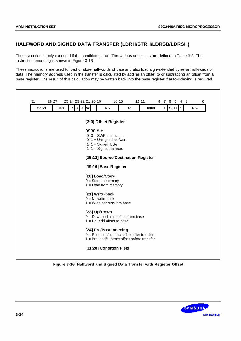
ARM INSTRUCTION SET S3C2440A RISC MICROPROCESSOR
3-34
HALFWORD AND SIGNED DATA TRANSFER (LDRH/STRH/LDRSB/LDRSH)
The instruction is only executed if the condition is true. The various conditions are defined in Table 3-2. Theinstruction encoding is shown in Figure 3-16.
These instructions are used to load or store half-words of data and also load sign-extended bytes or half-words ofdata. The memory address used in the transfer is calculated by adding an offset to or subtracting an offset from abase register. The result of this calculation may be written back into the base register if auto-indexing is required.
31 27 19 15
Cond
28 16 11122123
0
20
L Rn Rd
[3:0] Offset Register
[6][5] S H 0 0 = SWP instruction 0 1 = Unsigned halfword 1 1 = Signed byte 1 1 = Signed halfword
[15:12] Source/Destination Register
[19:16] Base Register
[20] Load/Store0 = Store to memory1 = Load from memory
[21] Write-back0 = No write-back1 = Write address into base
[23] Up/Down0 = Down: subtract offset from base1 = Up: add offset to base
[24] Pre/Post Indexing0 = Post: add/subtract offset after transfer1 = Pre: add/subtract offset bofore transfer
[31:28] Condition Field
22
000 P U 0000W
2425
1 RmS H 1
8 7 6 5 4 3 0
Figure 3-16. Halfword and Signed Data Transfer with Register Offset
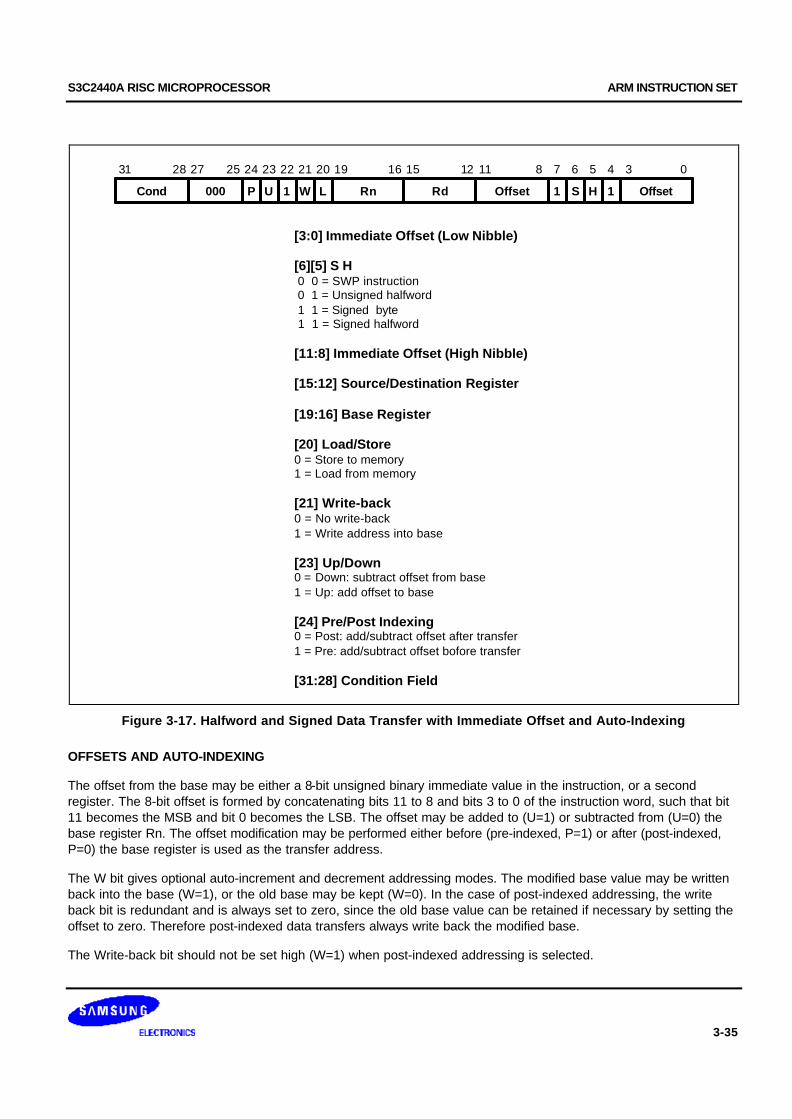
S3C2440A RISC MICROPROCESSOR ARM INSTRUCTION SET
3-35
31 27 19 15
Cond
28 16 11122123
1
20
L Rn Rd
[3:0] Immediate Offset (Low Nibble)
[6][5] S H 0 0 = SWP instruction 0 1 = Unsigned halfword 1 1 = Signed byte 1 1 = Signed halfword
[11:8] Immediate Offset (High Nibble)
[15:12] Source/Destination Register
[19:16] Base Register
[20] Load/Store0 = Store to memory1 = Load from memory
[21] Write-back0 = No write-back1 = Write address into base
[23] Up/Down0 = Down: subtract offset from base1 = Up: add offset to base
[24] Pre/Post Indexing0 = Post: add/subtract offset after transfer1 = Pre: add/subtract offset bofore transfer
[31:28] Condition Field
22
000 P U OffsetW
2425
1 OffsetS H 1
8 7 6 5 4 3 0
Figure 3-17. Halfword and Signed Data Transfer with Immediate Offset and Auto-Indexing
OFFSETS AND AUTO-INDEXING
The offset from the base may be either a 8-bit unsigned binary immediate value in the instruction, or a secondregister. The 8-bit offset is formed by concatenating bits 11 to 8 and bits 3 to 0 of the instruction word, such that bit11 becomes the MSB and bit 0 becomes the LSB. The offset may be added to (U=1) or subtracted from (U=0) thebase register Rn. The offset modification may be performed either before (pre-indexed, P=1) or after (post-indexed,P=0) the base register is used as the transfer address.
The W bit gives optional auto-increment and decrement addressing modes. The modified base value may be writtenback into the base (W=1), or the old base may be kept (W=0). In the case of post-indexed addressing, the writeback bit is redundant and is always set to zero, since the old base value can be retained if necessary by setting theoffset to zero. Therefore post-indexed data transfers always write back the modified base.
The Write-back bit should not be set high (W=1) when post-indexed addressing is selected.
ARM INSTRUCTION SET S3C2440A RISC MICROPROCESSOR
3-36
HALFWORD LOAD AND STORES
Setting S=0 and H=1 may be used to transfer unsigned Half-words between an ARM920T register and memory.
The action of LDRH and STRH instructions is influenced by the BIGEND control signal. The two possibleconfigurations are described in the section below.
Signed byte and halfword loads
The S bit controls the loading of sign-extended data. When S=1 the H bit selects between Bytes (H=0) and Half-words (H=1). The L bit should not be set low (Store) when Signed (S=1) operations have been selected.
The LDRSB instruction loads the selected Byte into bits 7 to 0 of the destination register and bits 31 to 8 of thedestination register are set to the value of bit 7, the sign bit.
The LDRSH instruction loads the selected Half-word into bits 15 to 0 of the destination register and bits 31 to 16 ofthe destination register are set to the value of bit 15, the sign bit.
The action of the LDRSB and LDRSH instructions is influenced by the BIGEND control signal. The two possibleconfigurations are described in the following section.
Endianness and byte/halfword selection
Little-Endian Configuration
A signed byte load (LDRSB) expects data on data bus inputs 7 through to 0 if the supplied address is on a wordboundary, on data bus inputs 15 through to 8 if it is a word address plus one byte, and so on. The selected byte isplaced in the bottom 8 bit of the destination register, and the remaining bits of the register are filled with the sign bit,bit 7 of the byte. Please see Figure 2-2.
A halfword load (LDRSH or LDRH) expects data on data bus inputs 15 through to 0 if the supplied address is on aword boundary and on data bus inputs 31 through to 16 if it is a halfword boundary, (A[1]=1).The supplied addressshould always be on a halfword boundary. If bit 0 of the supplied address is HIGH then the ARM920T will load anunpredictable value. The selected halfword is placed in the bottom 16 bits of the destination register. For unsignedhalf-words (LDRH), the top 16 bits of the register are filled with zeros and for signed half-words (LDRSH) the top 16bits are filled with the sign bit, bit 15 of the halfword.
A halfword store (STRH) repeats the bottom 16 bits of the source register twice across the data bus outputs 31through to 0. The external memory system should activate the appropriate halfword subsystem to store the data.Note that the address must be halfword aligned, if bit 0 of the address is HIGH this will cause unpredictablebehaviour.
S3C2440A RISC MICROPROCESSOR ARM INSTRUCTION SET
3-37
Big-Endian Configuration
A signed byte load (LDRSB) expects data on data bus inputs 31 through to 24 if the supplied address is on a wordboundary, on data bus inputs 23 through to 16 if it is a word address plus one byte, and so on. The selected byte isplaced in the bottom 8 bit of the destination register, and the remaining bits of the register are filled with the sign bit,bit 7 of the byte. Please see Figure 2-1.
A halfword load (LDRSH or LDRH) expects data on data bus inputs 31 through to 16 if the supplied address is on aword boundary and on data bus inputs 15 through to 0 if it is a halfword boundary, (A[1]=1). The supplied addressshould always be on a halfword boundary. If bit 0 of the supplied address is HIGH then the ARM920T will load anunpredictable value. The selected halfword is placed in the bottom 16 bits of the destination register. For unsignedhalf-words (LDRH), the top 16 bits of the register are filled with zeros and for signed half-words (LDRSH) the top 16bits are filled with the sign bit, bit 15 of the halfword.
A halfword store (STRH) repeats the bottom 16 bits of the source register twice across the data bus outputs 31through to 0. The external memory system should activate the appropriate halfword subsystem to store the data.
NOTE
Please note that the address must be halfword aligned, if bit 0 of the address is HIGH this will causeunpredictable behavior.
USE OF R15
Write-back should not be specified if R15 is specified as the base register (Rn). While using R15 as the baseregister you must remember it contains address 8 bytes on from the address of the current instruction.
R15 should not be specified as the register offset (Rm).
When R15 is the source register (Rd) of a Half-word store (STRH) instruction, the stored address will be address ofthe instruction plus 12.
DATA ABORTS
A transfer to or from a legal address may cause problems for a memory management system. For instance, in asystem which uses virtual memory the required data may be absent from the main memory. The memory managercan signal a problem by taking the processor ABORT input HIGH whereupon the Data Abort trap will be taken. It isup to the system software to resolve the cause of the problem, then the instruction can be restarted and the originalprogram continued.
INSTRUCTION CYCLE TIMES
Normal LDR(H,SH,SB) instructions take 1S + 1N + 1I. LDR(H,SH,SB) PC take 2S + 2N + 1I incremental cycles.S,N and I are defined as sequential (S-cycle), non-sequential (N-cycle), and internal (I-cycle), respectively. STRHinstructions take 2N incremental cycles to execute.
ARM INSTRUCTION SET S3C2440A RISC MICROPROCESSOR
3-38
ASSEMBLER SYNTAX
<LDR|STR>cond<H|SH|SB> Rd,<address>
LDR Load from memory into a register
STR Store from a register into memory
cond Two-character condition mnemonic. See Table 3-2.
H Transfer halfword quantity
SB Load sign extended byte (Only valid for LDR)
SH Load sign extended halfword (Only valid for LDR)
Rd An expression evaluating to a valid register number.
<address> can be:
1 An expression which generates an address:The assembler will attempt to generate an instruction using the PC as a base and a
corrected immediate offset to address the location given by evaluating the expression. This willbe a PC relative, pre-indexed address. If the address is out of range, an error will begenerated.
2 A pre-indexed addressing specification:[Rn] offset of zero[Rn,<#expression>]! offset of <expression> bytes[Rn,+/-Rm]! offset of +/- contents of index register
3 A post-indexed addressing specification:[Rn],<#expression> offset of <expression> bytes[Rn],+/-Rm offset of +/- contents of index register.
4 Rn and Rm are expressions evaluating to a register number. If Rn is R15 then theassembler will subtract 8 from the offset value to allow for ARM920T pipelining. In this case
base write-back should not be specified.
! Writes back the base register (set the W bit) if ! is present.
S3C2440A RISC MICROPROCESSOR ARM INSTRUCTION SET
3-39
EXAMPLES
LDRH R1,[R2,-R3]! ; Load R1 from the contents of the halfword address; contained in R2-R3 (both of which are registers); and write back address to R2
STRH R3,[R4,#14] ; Store the halfword in R3 at R14+14 but don't write back.LDRSB R8,[R2],#-223 ; Load R8 with the sign extended contents of the byte
; address contained in R2 and write back R2-223 to R2.LDRNESH R11,[R0] ; Conditionally load R11 with the sign extended contents
; of the halfword address contained in R0.HERE ; Generate PC relative offset to address FRED.STRH R5, [PC,#(FRED-HERE-8)]; Store the halfword in R5 at address FREDFRED
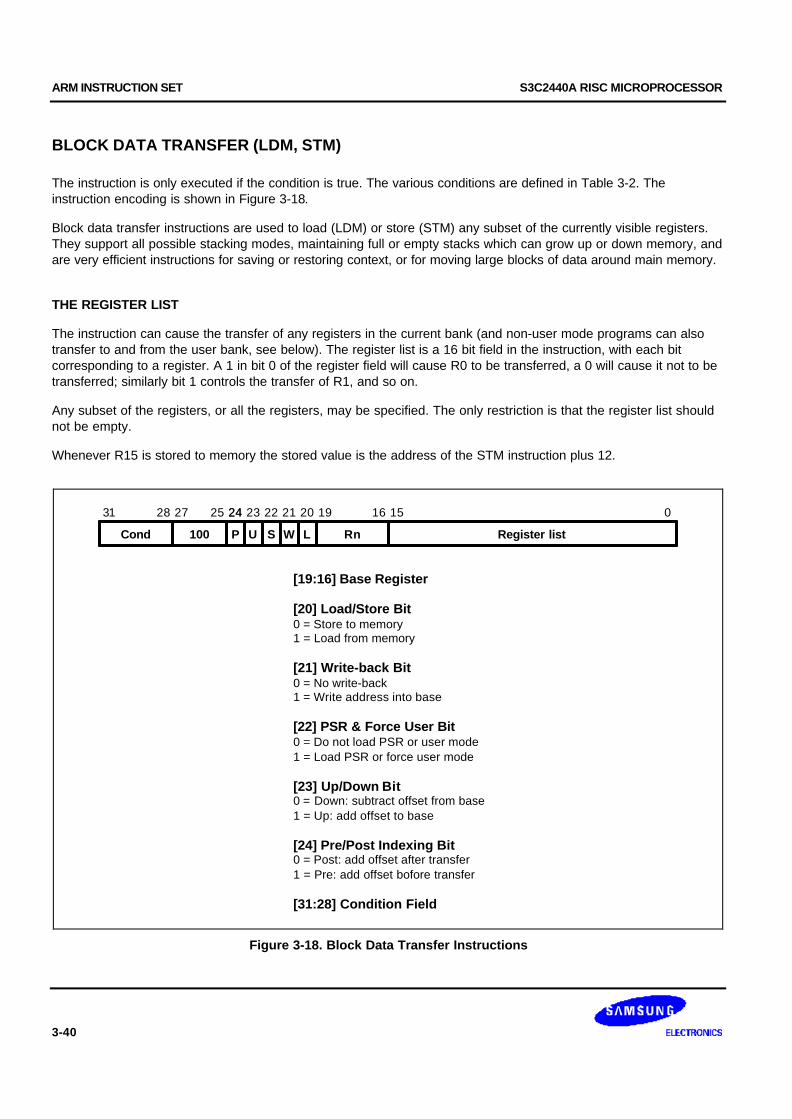
ARM INSTRUCTION SET S3C2440A RISC MICROPROCESSOR
3-40
BLOCK DATA TRANSFER (LDM, STM)
The instruction is only executed if the condition is true. The various conditions are defined in Table 3-2. Theinstruction encoding is shown in Figure 3-18.
Block data transfer instructions are used to load (LDM) or store (STM) any subset of the currently visible registers.They support all possible stacking modes, maintaining full or empty stacks which can grow up or down memory, andare very efficient instructions for saving or restoring context, or for moving large blocks of data around main memory.
THE REGISTER LIST
The instruction can cause the transfer of any registers in the current bank (and non-user mode programs can alsotransfer to and from the user bank, see below). The register list is a 16 bit field in the instruction, with each bitcorresponding to a register. A 1 in bit 0 of the register field will cause R0 to be transferred, a 0 will cause it not to betransferred; similarly bit 1 controls the transfer of R1, and so on.
Any subset of the registers, or all the registers, may be specified. The only restriction is that the register list shouldnot be empty.
Whenever R15 is stored to memory the stored value is the address of the STM instruction plus 12.
31 27 19 15
Cond
28 162123
S
20
L Rn
[19:16] Base Register
[20] Load/Store Bit0 = Store to memory1 = Load from memory
[21] Write-back Bit0 = No write-back1 = Write address into base
[22] PSR & Force User Bit0 = Do not load PSR or user mode1 = Load PSR or force user mode
[23] Up/Down Bit0 = Down: subtract offset from base1 = Up: add offset to base
[24] Pre/Post Indexing Bit0 = Post: add offset after transfer1 = Pre: add offset bofore transfer
[31:28] Condition Field
22
100 P U W
2425
Register list
24 0
Figure 3-18. Block Data Transfer Instructions

S3C2440A RISC MICROPROCESSOR ARM INSTRUCTION SET
3-41
ADDRESSING MODES
The transfer addresses are determined by the contents of the base register (Rn), the pre/post bit (P) and the up/down bit (U). The registers are transferred in the order lowest to highest, so R15 (if in the list) will always betransferred last. The lowest register also gets transferred to/from the lowest memory address. By way of illustration,consider the transfer of R1, R5 and R7 in the case where Rn=0x1000 and write back of the modified base is required(W=1). Figure 3.19-22 show the sequence of register transfers, the addresses used, and the value of Rn after theinstruction has completed.
In all cases, had write back of the modified base not been required (W=0), Rn would have retained its initial value of0x1000 unless it was also in the transfer list of a load multiple register instruction, when it would have beenoverwritten with the loaded value. (Please check the meaning again)*****
ADDRESS ALIGNMENT
The address should normally be a word aligned quantity and non-word aligned addresses should not affect theinstruction. However, the bottom 2 bits of the address will appear on A[1:0] and might be interpreted by the memorysystem.
1 2
3 4
Rn R1
R1R5
R1R5R7
Rn
0x100C
0x1000
0x0FF4
0x100C
0x1000
0x0FF4
0x100C
0x1000
0x0FF4
0x100C
0x1000
0x0FF4
Figure 3-19. Post-Increment Addressing
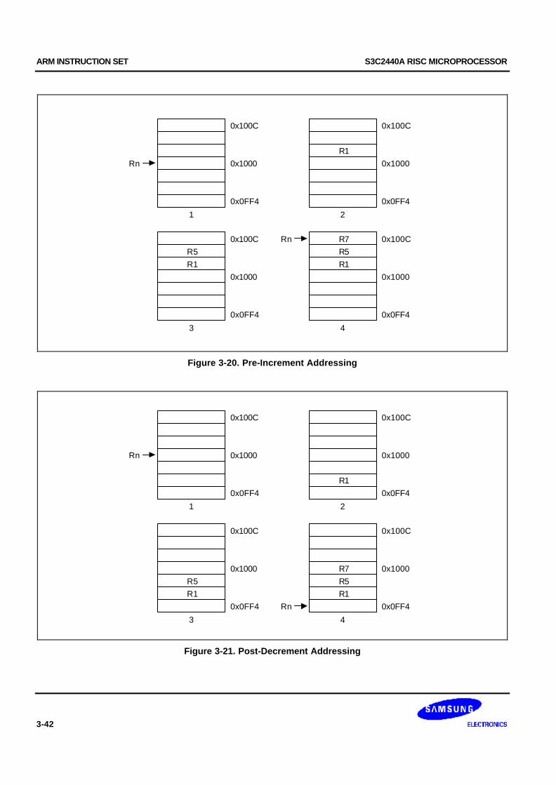
ARM INSTRUCTION SET S3C2440A RISC MICROPROCESSOR
3-42
Rn
1
R1
R1
2
R5
3
R1R5
4
R7Rn
0x100C
0x1000
0x0FF4
0x100C
0x1000
0x0FF4
0x100C
0x1000
0x0FF4
0x100C
0x1000
0x0FF4
Figure 3-20. Pre-Increment Addressing
Rn
1
R1
R1
2
R5
3
R1R5
4
R7
Rn
0x100C
0x1000
0x0FF4
0x100C
0x1000
0x0FF4
0x100C
0x1000
0x0FF4
0x100C
0x1000
0x0FF4
Figure 3-21. Post-Decrement Addressing

S3C2440A RISC MICROPROCESSOR ARM INSTRUCTION SET
3-43
Rn
1
R1
R1
2
R5
3
R1R5
4
R7
Rn
0x100C
0x1000
0x0FF4
0x100C
0x1000
0x0FF4
0x100C
0x1000
0x0FF4
0x100C
0x1000
0x0FF4
Figure 3-22. Pre-Decrement Addressing
USE OF THE S BIT
When the S bit is set in a LDM/STM instruction it depends on R15 is available in the transfer list and on the type ofinstruction. The S bit should only be set if the instruction is to execute in a privileged mode.
LDM with R15 in Transfer List and S Bit Set (Mode Changes)
If the instruction is a LDM then SPSR_<mode> is transferred to CPSR at the same time as R15 is loaded.
STM with R15 in Transfer List and S Bit Set (User Bank Transfer)
The registers transferred are taken from the User bank rather than the bank corresponding to the current mode. Thisis useful for saving the user state on process switches. Base write-back should not be used when this mechanism isemployed.
R15 not in List and S Bit Set (User Bank Transfer)
For both LDM and STM instructions, the User bank registers are transferred rather than the register bankcorresponding to the current mode. This is useful for saving the user state on process switches. Base write-backshould not be used when this mechanism is employed.
When the instruction is LDM, care must be taken not to read from a banked register during the following cycle(inserting a dummy instruction such as MOV R0, R0 after the LDM will ensure safety).
USE OF R15 AS THE BASE
R15 should not be used as the base register in any LDM or STM instruction.
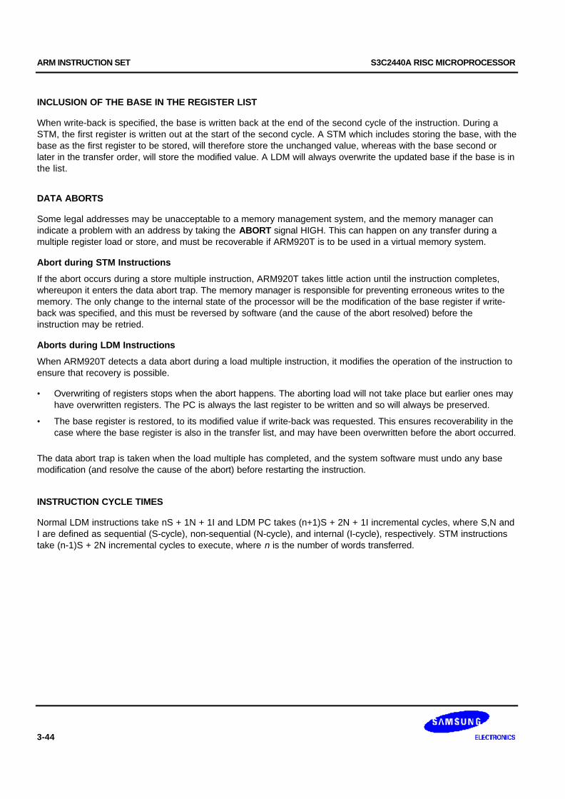
ARM INSTRUCTION SET S3C2440A RISC MICROPROCESSOR
3-44
INCLUSION OF THE BASE IN THE REGISTER LIST
When write-back is specified, the base is written back at the end of the second cycle of the instruction. During aSTM, the first register is written out at the start of the second cycle. A STM which includes storing the base, with thebase as the first register to be stored, will therefore store the unchanged value, whereas with the base second orlater in the transfer order, will store the modified value. A LDM will always overwrite the updated base if the base is inthe list.
DATA ABORTS
Some legal addresses may be unacceptable to a memory management system, and the memory manager canindicate a problem with an address by taking the ABORT signal HIGH. This can happen on any transfer during amultiple register load or store, and must be recoverable if ARM920T is to be used in a virtual memory system.
Abort during STM Instructions
If the abort occurs during a store multiple instruction, ARM920T takes little action until the instruction completes,whereupon it enters the data abort trap. The memory manager is responsible for preventing erroneous writes to thememory. The only change to the internal state of the processor will be the modification of the base register if write-back was specified, and this must be reversed by software (and the cause of the abort resolved) before theinstruction may be retried.
Aborts during LDM Instructions
When ARM920T detects a data abort during a load multiple instruction, it modifies the operation of the instruction toensure that recovery is possible.
• Overwriting of registers stops when the abort happens. The aborting load will not take place but earlier ones mayhave overwritten registers. The PC is always the last register to be written and so will always be preserved.
• The base register is restored, to its modified value if write-back was requested. This ensures recoverability in thecase where the base register is also in the transfer list, and may have been overwritten before the abort occurred.
The data abort trap is taken when the load multiple has completed, and the system software must undo any basemodification (and resolve the cause of the abort) before restarting the instruction.
INSTRUCTION CYCLE TIMES
Normal LDM instructions take nS + 1N + 1I and LDM PC takes (n+1)S + 2N + 1I incremental cycles, where S,N andI are defined as sequential (S-cycle), non-sequential (N-cycle), and internal (I-cycle), respectively. STM instructionstake (n-1)S + 2N incremental cycles to execute, where n is the number of words transferred.

S3C2440A RISC MICROPROCESSOR ARM INSTRUCTION SET
3-45
ASSEMBLER SYNTAX
<LDM|STM>cond<FD|ED|FA|EA|IA|IB|DA|DB> Rn!,<Rlist>^
where:
cond Two character condition mnemonic. See Table 3-2.
Rn An expression evaluating to a valid register number
<Rlist> A list of registers and register ranges enclosed in (e.g. R0,R2-R7,R10).
! If present requests write-back (W=1), otherwise W=0.
^ If present set S bit to load the CPSR along with the PC, or force transfer of user bankwhen in privileged mode.
Addressing Mode Names
There are different assembler mnemonics for each of the addressing modes, depending on whether the instruction isbeing used to support stacks or for other purposes. The equivalence between the names and the values of the bits inthe instruction are shown in the following table 3-6.
Table 3-6. Addressing Mode Names
Name Stack Other L Bit P Bit U Bit
Pre-Increment Load LDMED LDMIB 1 1 1
Post-Increment Load LDMFD LDMIA 1 0 1
Pre-Decrement Load LDMEA LDMDB 1 1 0
Post-Decrement Load LDMFA LDMDA 1 0 0
Pre-Increment Store STMFA STMIB 0 1 1
Post-Increment Store STMEA STMIA 0 0 1
Pre-Decrement Store STMFD STMDB 0 1 0
Post-Decrement Store STMED STMDA 0 0 0
FD, ED, FA, EA define pre/post indexing and the up/down bit by reference to the form of stack required. The F and Erefer to a "full" or "empty" stack, i.e. whether a pre-index has to be done (full) before storing to the stack. The A andD refer to whether the stack is ascending or descending. If ascending, a STM will go up and LDM down, ifdescending, vice-versa.
IA, IB, DA, DB allow control when LDM/STM are not being used for stacks and simply mean Increment After,Increment Before, Decrement After, Decrement Before.
ARM INSTRUCTION SET S3C2440A RISC MICROPROCESSOR
3-46
EXAMPLES
LDMFD SP!,R0,R1,R2 ; Unstack 3 registers.STMIA R0,R0-R15 ; Save all registers.LDMFD SP!,R15 ; R15 ← (SP), CPSR unchanged.LDMFD SP!,R15^ ; R15 ← (SP), CPSR <- SPSR_mode
; (allowed only in privileged modes).STMFD R13,R0-R14^ ; Save user mode regs on stack
; (allowed only in privileged modes).
These instructions may be used to save state on subroutine entry, and restore it efficiently on return to the callingroutine:
STMED SP!,R0-R3,R14 ; Save R0 to R3 to use as workspace; and R14 for returning.
BL somewhere ; This nested call will overwrite R14LDMED SP!,R0-R3,R15 ; Restore workspace and return.
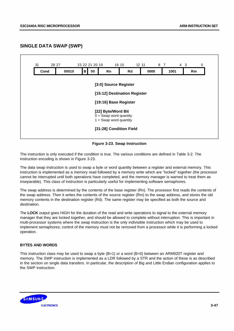
S3C2440A RISC MICROPROCESSOR ARM INSTRUCTION SET
3-47
SINGLE DATA SWAP (SWP)
31 19 15
Cond
28 16 11122123
B
20
00 Rn Rd
[3:0] Source Register
[15:12] Destination Register
[19:16] Base Register [22] Byte/Word Bit0 = Swap word quantity1 = Swap word quantity
[31:28] Condition Field
22
00010 0000 Rm1001
27 8 7 4 3 0
Figure 3-23. Swap Instruction
The instruction is only executed if the condition is true. The various conditions are defined in Table 3-2. Theinstruction encoding is shown in Figure 3-23.
The data swap instruction is used to swap a byte or word quantity between a register and external memory. Thisinstruction is implemented as a memory read followed by a memory write which are “locked” together (the processorcannot be interrupted until both operations have completed, and the memory manager is warned to treat them asinseparable). This class of instruction is particularly useful for implementing software semaphores.
The swap address is determined by the contents of the base register (Rn). The processor first reads the contents ofthe swap address. Then it writes the contents of the source register (Rm) to the swap address, and stores the oldmemory contents in the destination register (Rd). The same register may be specified as both the source anddestination.
The LOCK output goes HIGH for the duration of the read and write operations to signal to the external memorymanager that they are locked together, and should be allowed to complete without interruption. This is important inmulti-processor systems where the swap instruction is the only indivisible instruction which may be used toimplement semaphores; control of the memory must not be removed from a processor while it is performing a lockedoperation.
BYTES AND WORDS
This instruction class may be used to swap a byte (B=1) or a word (B=0) between an ARM920T register andmemory. The SWP instruction is implemented as a LDR followed by a STR and the action of these is as describedin the section on single data transfers. In particular, the description of Big and Little Endian configuration applies tothe SWP instruction.
ARM INSTRUCTION SET S3C2440A RISC MICROPROCESSOR
3-48
USE OF R15
Do not use R15 as an operand (Rd, Rn or Rs) in a SWP instruction.
DATA ABORTS
If the address used for the swap is unacceptable to a memory management system, the memory manager can flagthe problem by driving ABORT HIGH. This can happen on either the read or the write cycle (or both), and in eithercase, the Data Abort trap will be taken. It is up to the system software to resolve the cause of the problem, then theinstruction can be restarted and the original program continued.
INSTRUCTION CYCLE TIMES
Swap instructions take 1S + 2N +1I incremental cycles to execute, where S,N and I are defined as sequential(S-cycle), non-sequential, and internal (I-cycle), respectively.
ASSEMBLER SYNTAX
<SWP>condB Rd,Rm,[Rn]
cond Two-character condition mnemonic. See Table 3-2.
B If B is present then byte transfer, otherwise word transfer
Rd,Rm,Rn Expressions evaluating to valid register numbers
Examples
SWP R0,R1,[R2] ; Load R0 with the word addressed by R2, and; store R1 at R2.
SWPB R2,R3,[R4] ; Load R2 with the byte addressed by R4, and; store bits 0 to 7 of R3 at R4.
SWPEQ R0,R0,[R1] ; Conditionally swap the contents of the; word addressed by R1 with R0.

S3C2440A RISC MICROPROCESSOR ARM INSTRUCTION SET
3-49
SOFTWARE INTERRUPT (SWI)
The instruction is only executed if the condition is true. The various conditions are defined in Table 3-2. Theinstruction encoding is shown in Figure 3-24, below.
31 2427
1111Cond Comment Field (Ignored by Processor)
28 23
[31:28] Condition Field
0
Figure 3-24. Software Interrupt Instruction
The software interrupt instruction is used to enter Supervisor mode in a controlled manner. The instruction causesthe software interrupt trap to be taken, which effects the mode change. The PC is then forced to a fixed value (0x08)and the CPSR is saved in SPSR_svc. If the SWI vector address is suitably protected (by external memorymanagement hardware) from modification by the user, a fully protected operating system may be constructed.
RETURN FROM THE SUPERVISOR
The PC is saved in R14_svc upon entering the software interrupt trap, with the PC adjusted to point to the word afterthe SWI instruction. MOVS PC,R14_svc will return to the calling program and restore the CPSR.
Note that the link mechanism is not re-entrant, so if the supervisor code wishes to use software interrupts withinitself it must first save a copy of the return address and SPSR.
COMMENT FIELD
The bottom 24 bits of the instruction are ignored by the processor, and may be used to communicate information tothe supervisor code. For instance, the supervisor may look at this field and use it to index into an array of entrypoints for routines which perform the various supervisor functions.
INSTRUCTION CYCLE TIMES
Software interrupt instructions take 2S + 1N incremental cycles to execute, where S and N are defined as sequential(S-cycle) and non-sequential (N-cycle).
ARM INSTRUCTION SET S3C2440A RISC MICROPROCESSOR
3-50
ASSEMBLER SYNTAX
SWIcond <expression>
cond Two character condition mnemonic, Table 3-2.
<expression> Evaluated and placed in the comment field (which is ignored by ARM920T).
Examples
SWI ReadC ; Get next character from read stream.SWI WriteI+"k” ; Output a "k" to the write stream.SWINE 0 ; Conditionally call supervisor with 0 in comment field.
Supervisor code
The previous examples assume that suitable supervisor code exists, for instance:
0x08 B Supervisor ; SWI entry pointEntryTable ; Addresses of supervisor routinesDCD ZeroRtnDCD ReadCRtnDCD WriteIRtn• • •Zero EQU 0
ReadC EQU 256WriteI EQU 512
Supervisor ; SWI has routine required in bits 8-23 and data (if any) in; bits 0-7. Assumes R13_svc points to a suitable stack
STMFD R13,R0-R2,R14 ; Save work registers and return address.LDR R0,[R14,#-4] ; Get SWI instruction.BIC R0,R0,#0xFF000000 ; Clear top 8 bits.MOV R1,R0,LSR#8 ; Get routine offset.ADR R2,EntryTable ; Get start address of entry table.LDR R15,[R2,R1,LSL#2] ; Branch to appropriate routine.WriteIRtn ; Enter with character in R0 bits 0-7.• • •LDMFD R13,R0-R2,R15^ ; Restore workspace and return,
; restoring processor mode and flags.

S3C2440A RISC MICROPROCESSOR ARM INSTRUCTION SET
3-51
COPROCESSOR DATA OPERATIONS (CDP)
The instruction is only executed if the condition is true. The various conditions are defined in Table 3-2. Theinstruction encoding is shown in Figure 3-25.
This class of instruction is used to tell a coprocessor to perform some internal operation. No result is communicatedback to ARM920T, and it will not wait for the operation to complete. The coprocessor could contain a queue of suchinstructions awaiting execution, and their execution can overlap other activity, allowing the coprocessor andARM920T to perform independent tasks in parallel.
COPROCESSOR INSTRUCTIONS
The S3C2440A, unlike some other ARM-based processors, does not have an external coprocessor interface. It doesnot have a on-chip coprocessor also.
So then all coprocessor instructions will cause the undefined instruction trap to be taken on the S3C2440A. Thesecoprocessor instructions can be emulated by the undefined trap handler. Even though external coprocessor can notbe connected to the S3C2440A, the coprocessor instructions are still described here in full for completeness.(Remember that any external coprocessor described in this section is a software emulation.)
31 2427 19 15
Cond CRm
28 16 111223 20
[3:0] Coprocessor operand register
[7:5] Coprocessor information
[11:8] Coprocessor number
[15:12] Coprocessor destination register
[19:16] Coprocessor operand register
[23:20] Coprocessor operation code
[31:28] Condition Field
0CpCp#CRdCRn1110 CP Opc
8 7 5 4 3 0
Figure 3-25. Coprocessor Data Operation Instruction
Only bit 4 and bits 24 to 31 The coprocessor fields are significant to ARM920T. The remaining bits are used bycoprocessors. The above field names are used by convention, and particular coprocessors may redefine the use ofall fields except CP# as appropriate. The CP# field is used to contain an identifying number (in the range 0 to 15) foreach coprocessor, and a coprocessor will ignore any instruction which does not contain its number in the CP# field.
The conventional interpretation of the instruction is that the coprocessor should perform an operation specified in theCP Opc field (and possibly in the CP field) on the contents of CRn and CRm, and place the result in CRd.
ARM INSTRUCTION SET S3C2440A RISC MICROPROCESSOR
3-52
INSTRUCTION CYCLE TIMES
Coprocessor data operations take 1S + bI incremental cycles to execute, where b is the number of cycles spent inthe coprocessor busy-wait loop.
S and I are defined as sequential (S-cycle) and internal (I-cycle).
Assembler syntax
CDPcond p#,<expression1>,cd,cn,cm,<expression2>
cond Two character condition mnemonic. See Table 3-2.
p# The unique number of the required coprocessor
<expression1> Evaluated to a constant and placed in the CP Opc field
cd, cn and cm Evaluate to the valid coprocessor register numbers CRd, CRn and CRm respectively
<expression2> Where present is evaluated to a constant and placed in the CP field
EXAMPLES
CDP p1,10,c1,c2,c3 ; Request coproc 1 to do operation 10; on CR2 and CR3, and put the result in CR1.
CDPEQ p2,5,c1,c2,c3,2 ; If Z flag is set request coproc 2 to do operation 5 (type 2); on CR2 and CR3, and put the result in CR1.
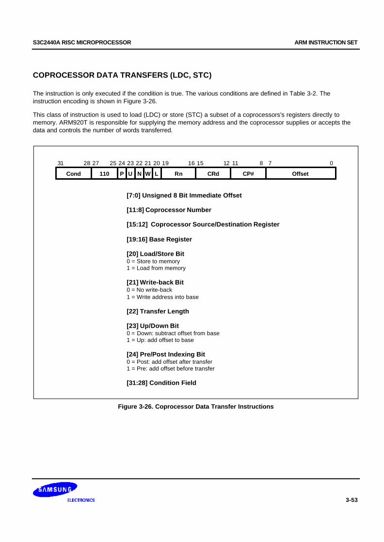
S3C2440A RISC MICROPROCESSOR ARM INSTRUCTION SET
3-53
COPROCESSOR DATA TRANSFERS (LDC, STC)
The instruction is only executed if the condition is true. The various conditions are defined in Table 3-2. Theinstruction encoding is shown in Figure 3-26.
This class of instruction is used to load (LDC) or store (STC) a subset of a coprocessors's registers directly tomemory. ARM920T is responsible for supplying the memory address and the coprocessor supplies or accepts thedata and controls the number of words transferred.
[7:0] Unsigned 8 Bit Immediate Offset
[11:8] Coprocessor Number
[15:12] Coprocessor Source/Destination Register
[19:16] Base Register
[20] Load/Store Bit0 = Store to memory1 = Load from memory
[21] Write-back Bit0 = No write-back1 = Write address into base
[22] Transfer Length
[23] Up/Down Bit0 = Down: subtract offset from base1 = Up: add offset to base
[24] Pre/Post Indexing Bit0 = Post: add offset after transfer1 = Pre: add offset before transfer
[31:28] Condition Field
31 27 19 15
Cond
28 16 11122123
N
20
L Rn CRd
22
110 P U CP#W
2425
Offset
8 7 0
Figure 3-26. Coprocessor Data Transfer Instructions
ARM INSTRUCTION SET S3C2440A RISC MICROPROCESSOR
3-54
THE COPROCESSOR FIELDS
The CP# field is used to identify the coprocessor which is required to supply or accept the data, and a coprocessorwill only respond if its number matches the contents of this field.
The CRd field and the N bit contain information for the coprocessor which may be interpreted in different ways bydifferent coprocessors, but by convention CRd is the register to be transferred (or the first register where more thanone is to be transferred), and the N bit is used to choose one of two transfer length options. For instance N=0 couldselect the transfer of a single register, and N=1 could select the transfer of all the registers for context switching.
ADDRESSING MODES
ARM920T is responsible for providing the address used by the memory system for the transfer, and the addressingmodes available are a subset of those used in single data transfer instructions. Note, however, that the immediateoffsets are 8 bits wide and specify word offsets for coprocessor data transfers, whereas they are 12 bits wide andspecify byte offsets for single data transfers.
The 8 bit unsigned immediate offset is shifted left 2 bits and either added to (U=1) or subtracted from (U=0) the baseregister (Rn); this calculation may be performed either before (P=1) or after (P=0) the base is used as the transferaddress. The modified base value may be overwritten back into the base register (if W=1), or the old value of thebase may be preserved (W=0). Note that post-indexed addressing modes require explicit setting of the W bit, unlikeLDR and STR which always write-back when post-indexed.
The value of the base register, modified by the offset in a pre-indexed instruction, is used as the address for thetransfer of the first word. The second word (if more than one is transferred) will go to or come from an address oneword (4 bytes) higher than the first transfer, and the address will be incremented by one word for each subsequenttransfer.
ADDRESS ALIGNMENT
The base address should normally be a word aligned quantity. The bottom 2 bits of the address will appear on A[1:0]and might be interpreted by the memory system.
Use of R15
If Rn is R15, the value used will be the address of the instruction plus 8 bytes. Base write-back to R15 must not bespecified.
DATA ABORTS
If the address is legal but the memory manager generates an abort, the data trap will be taken. The write-back of themodified base will take place, but all other processor state will be preserved. The coprocessor is partly responsiblefor ensuring that the data transfer can be restarted after the cause of the abort has been resolved, and must ensurethat any subsequent actions it undertakes can be repeated when the instruction is retried.
Instruction cycle times
Coprocessor data transfer instructions take (n-1)S + 2N + bI incremental cycles to execute, where:
n The number of words transferred.
b The number of cycles spent in the coprocessor busy-wait loop.
S, N and I are defined as sequential (S-cycle), non-sequential (N-cycle), and internal (I-cycle), respectively.
S3C2440A RISC MICROPROCESSOR ARM INSTRUCTION SET
3-55
ASSEMBLER SYNTAX
<LDC|STC>condL p#,cd,<Address>
LDC Load from memory to coprocessor
STC Store from coprocessor to memory
L When present perform long transfer (N=1), otherwise perform short transfer (N=0)
cond Two character condition mnemonic. See Table 3-2..
p# The unique number of the required coprocessor
cd An expression evaluating to a valid coprocessor register number that is placed in theCRd field
<Address> can be:
1 An expression which generates an address:The assembler will attempt to generate an instruction using the PC as a base and a corrected immediate offset to address the location given by evaluating the expression.This will be a PC relative, pre-indexed address. If the address is out of range, an errorwill be generated
2 A pre-indexed addressing specification:[Rn] offset of zero[Rn,<#expression>]! offset of <expression> bytes
3 A post-indexed addressing specification:[Rn],<#expression offset of <expression> bytes! write back the base register (set the W bit) if! is presentRn is an expression evaluating to a valid
ARM920T register number.
NOTE
If Rn is R15, the assembler will subtract 8 from the offset value to allow for ARM920T pipelining.
EXAMPLES
LDC p1,c2,table ; Load c2 of coproc 1 from address; table, using a PC relative address.
STCEQL p2,c3,[R5,#24]! ; Conditionally store c3 of coproc 2; into an address 24 bytes up from R5,; write this address back to R5, and use; long transfer option (probably to store multiple words).
NOTE
Although the address offset is expressed in bytes, the instruction offset field is in words. The assembler willadjust the offset appropriately.
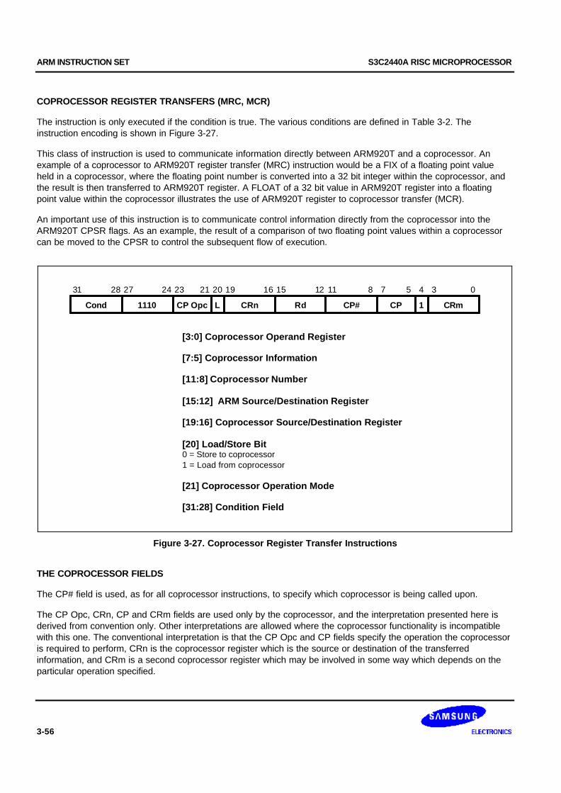
ARM INSTRUCTION SET S3C2440A RISC MICROPROCESSOR
3-56
COPROCESSOR REGISTER TRANSFERS (MRC, MCR)
The instruction is only executed if the condition is true. The various conditions are defined in Table 3-2. Theinstruction encoding is shown in Figure 3-27.
This class of instruction is used to communicate information directly between ARM920T and a coprocessor. Anexample of a coprocessor to ARM920T register transfer (MRC) instruction would be a FIX of a floating point valueheld in a coprocessor, where the floating point number is converted into a 32 bit integer within the coprocessor, andthe result is then transferred to ARM920T register. A FLOAT of a 32 bit value in ARM920T register into a floatingpoint value within the coprocessor illustrates the use of ARM920T register to coprocessor transfer (MCR).
An important use of this instruction is to communicate control information directly from the coprocessor into theARM920T CPSR flags. As an example, the result of a comparison of two floating point values within a coprocessorcan be moved to the CPSR to control the subsequent flow of execution.
31 27 19 15
Cond
28 16 11122123 20
L CRn Rd
[3:0] Coprocessor Operand Register
[7:5] Coprocessor Information
[11:8] Coprocessor Number
[15:12] ARM Source/Destination Register
[19:16] Coprocessor Source/Destination Register
[20] Load/Store Bit0 = Store to coprocessor1 = Load from coprocessor
[21] Coprocessor Operation Mode
[31:28] Condition Field
1110 CP Opc CP#
24
CRm1CP
8 7 5 4 3 0
Figure 3-27. Coprocessor Register Transfer Instructions
THE COPROCESSOR FIELDS
The CP# field is used, as for all coprocessor instructions, to specify which coprocessor is being called upon.
The CP Opc, CRn, CP and CRm fields are used only by the coprocessor, and the interpretation presented here isderived from convention only. Other interpretations are allowed where the coprocessor functionality is incompatiblewith this one. The conventional interpretation is that the CP Opc and CP fields specify the operation the coprocessoris required to perform, CRn is the coprocessor register which is the source or destination of the transferredinformation, and CRm is a second coprocessor register which may be involved in some way which depends on theparticular operation specified.
S3C2440A RISC MICROPROCESSOR ARM INSTRUCTION SET
3-57
TRANSFERS TO R15
When a coprocessor register transfer to ARM920T has R15 as the destination, bits 31, 30, 29 and 28 of thetransferred word are copied into the N, Z, C and V flags respectively. The other bits of the transferred word areignored, and the PC and other CPSR bits are unaffected by the transfer.
TRANSFERS FROM R15
A coprocessor register transfer from ARM920T with R15 as the source register will store the PC+12.
INSTRUCTION CYCLE TIMES
MRC instructions take 1S + (b+1)I +1C incremental cycles to execute, where S, I and C are defined as sequential(S-cycle), internal (I-cycle), and coprocessor register transfer (C-cycle), respectively. MCR instructions take 1S + bI+1C incremental cycles to execute, where b is the number of cycles spent in the coprocessor busy-wait loop.
ASSEMBLER SYNTAX
<MCR|MRC>cond p#,<expression1>,Rd,cn,cm,<expression2>
MRC Move from coprocessor to ARM920T register (L=1)
MCR Move from ARM920T register to coprocessor (L=0)
cond Two character condition mnemonic. See Table 3-2
p# The unique number of the required coprocessor
<expression1> Evaluated to a constant and placed in the CP Opc field
Rd An expression evaluating to a valid ARM920T register number
cn and cm Expressions evaluating to the valid coprocessor register numbers CRn and CRmrespectively
<expression2> Where present is evaluated to a constant and placed in the CP field
EXAMPLES
MRC p2,5,R3,c5,c6 ; Request coproc 2 to perform operation 5; on c5 and c6, and transfer the (single; 32-bit word) result back to R3.
MCR p6,0,R4,c5,c6 ; Request coproc 6 to perform operation 0; on R4 and place the result in c6.
MRCEQ p3,9,R3,c5,c6,2 ; Conditionally request coproc 3 to; perform operation 9 (type 2) on c5 and; c6, and transfer the result back to R3.
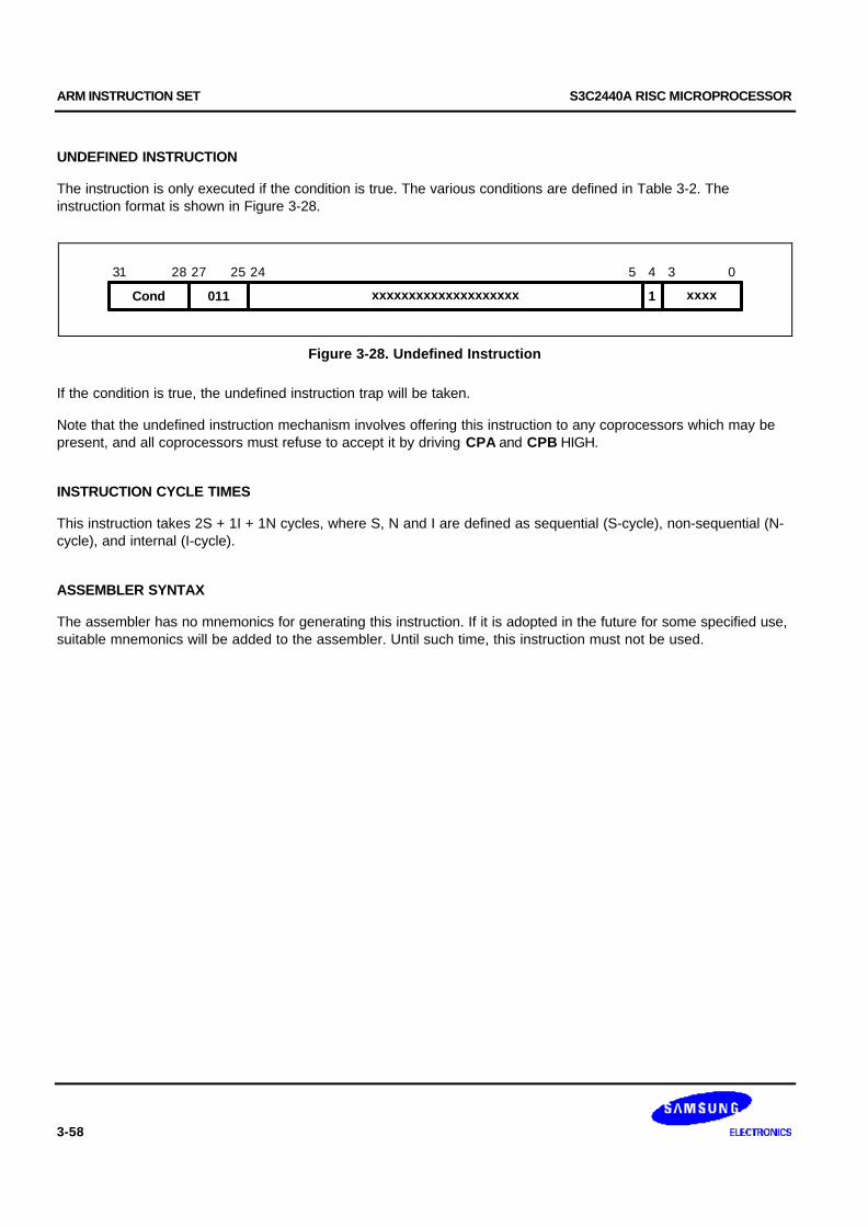
ARM INSTRUCTION SET S3C2440A RISC MICROPROCESSOR
3-58
UNDEFINED INSTRUCTION
The instruction is only executed if the condition is true. The various conditions are defined in Table 3-2. Theinstruction format is shown in Figure 3-28.
31 27
Cond
28 25 24
011 xxxxxxxxxxxxxxxxxxxx 1 xxxx
5 4 3 0
Figure 3-28. Undefined Instruction
If the condition is true, the undefined instruction trap will be taken.
Note that the undefined instruction mechanism involves offering this instruction to any coprocessors which may bepresent, and all coprocessors must refuse to accept it by driving CPA and CPB HIGH.
INSTRUCTION CYCLE TIMES
This instruction takes 2S + 1I + 1N cycles, where S, N and I are defined as sequential (S-cycle), non-sequential (N-cycle), and internal (I-cycle).
ASSEMBLER SYNTAX
The assembler has no mnemonics for generating this instruction. If it is adopted in the future for some specified use,suitable mnemonics will be added to the assembler. Until such time, this instruction must not be used.
S3C2440A RISC MICROPROCESSOR ARM INSTRUCTION SET
3-59
INSTRUCTION SET EXAMPLES
The following examples show ways in which the basic ARM920T instructions can combine to give efficient code.None of these methods saves a great deal of execution time (although they may save some), mostly they just savecode.
USING THE CONDITIONAL INSTRUCTIONS
Using Conditionals for Logical OR
CMP Rn,#p ; If Rn=p OR Rm=q THEN GOTO Label.BEQ LabelCMP Rm,#qBEQ Label
This can be replaced by
CMP Rn,#pCMPNE Rm,#q ; If condition not satisfied try other test.BEQ Label
Absolute Value
TEQ Rn,#0 ; Test signRSBMI Rn,Rn,#0 ; and 2's complement if necessary.
Multiplication by 4, 5 or 6 (Run Time)
MOV Rc,Ra,LSL#2 ; Multiply by 4,CMP Rb,#5 ; Test value,ADDCS Rc,Rc,Ra ; Complete multiply by 5,ADDHI Rc,Rc,Ra ; Complete multiply by 6.
Combining Discrete and Range Tests
TEQ Rc,#127 ; Discrete test,CMPNE Rc,# " "-1 ; Range testMOVLS Rc,# "" ; IF Rc<= "" OR Rc=ASCII(127)
; THEN Rc:= "."
ARM INSTRUCTION SET S3C2440A RISC MICROPROCESSOR
3-60
Division and Remainder
A number of divide routines for specific applications are provided in source form as part of the ANSI C library providedwith the ARM Cross Development Toolkit, available from your supplier. A short general purpose divide routine follows.
; Enter with numbers in Ra and Rb.MOV Rcnt,#1 ; Bit to control the division.
Div1 CMP Rb,#0x80000000 ; Move Rb until greater than Ra.CMPCC Rb,RaMOVCC Rb,Rb,ASL#1MOVCC Rcnt,Rcnt,ASL#1BCC Div1MOV Rc,#0
Div2 CMP Ra,Rb ; Test for possible subtraction.SUBCS Ra,Ra,Rb ; Subtract if ok,ADDCS Rc,Rc,Rcnt ; Put relevant bit into resultMOVS Rcnt,Rcnt,LSR#1 ; Shift control bitMOVNE Rb,Rb,LSR#1 ; Halve unless finished.BNE Div2 ; Divide result in Rc, remainder in Ra.
Overflow Detection in the ARM920T
1. Overflow in unsigned multiply with a 32-bit result
UMULL Rd,Rt,Rm,Rn ; 3 to 6 cyclesTEQ Rt,#0 ; +1 cycle and a registerBNE overflow
2. Overflow in signed multiply with a 32-bit result
SMULL Rd,Rt,Rm,Rn ; 3 to 6 cyclesTEQ Rt,Rd ASR#31 ; +1 cycle and a registerBNE overflow
3. Overflow in unsigned multiply accumulate with a 32 bit result
UMLAL Rd,Rt,Rm,Rn ; 4 to 7 cyclesTEQ Rt,#0 ; +1 cycle and a registerBNE overflow
4. Overflow in signed multiply accumulate with a 32 bit result
SMLAL Rd,Rt,Rm,Rn ; 4 to 7 cyclesTEQ Rt,Rd, ASR#31 ; +1 cycle and a registerBNE overflow

S3C2440A RISC MICROPROCESSOR ARM INSTRUCTION SET
3-61
5. Overflow in unsigned multiply accumulate with a 64 bit result
UMULL Rl,Rh,Rm,Rn ; 3 to 6 cyclesADDS Rl,Rl,Ra1 ; Lower accumulateADC Rh,Rh,Ra2 ; Upper accumulateBCS overflow ; 1 cycle and 2 registers
6. Overflow in signed multiply accumulate with a 64 bit result
SMULL Rl,Rh,Rm,Rn ; 3 to 6 cyclesADDS Rl,Rl,Ra1 ; Lower accumulateADC Rh,Rh,Ra2 ; Upper accumulateBVS overflow ; 1 cycle and 2 registers
NOTE
Overflow checking is not applicable to unsigned and signed multiplies with a 64-bit result, since overflowdoes not occur in such calculations.
PSEUDO-RANDOM BINARY SEQUENCE GENERATOR
It is often necessary to generate (pseudo-) random numbers and the most efficient algorithms are based on shiftgenerators with exclusive-OR feedback rather like a cyclic redundancy check generator. Unfortunately the sequenceof a 32 bit generator needs more than one feedback tap to be maximal length (i.e. 2^32-1 cycles before repetition),so this example uses a 33 bit register with taps at bits 33 and 20. The basic algorithm is newbit:=bit 33 eor bit 20,shift left the 33 bit number and put in newbit at the bottom; this operation is performed for all the newbits needed (i.e.32 bits). The entire operation can be done in 5 S cycles:
; Enter with seed in Ra (32 bits),; Rb (1 bit in Rb lsb), uses Rc.
TST Rb,Rb,LSR#1 ; Top bit into carryMOVS Rc,Ra,RRX ; 33 bit rotate rightADC Rb,Rb,Rb ; Carry into lsb of RbEOR Rc,Rc,Ra,LSL#12 ; (involved!)
EOR Ra,Rc,Rc,LSR#20 ; (similarly involved!) new seed in Ra, Rb as before
MULTIPLICATION BY CONSTANT USING THE BARREL SHIFTER
Multiplication by 2^n (1,2,4,8,16,32..)
MOV Ra, Rb, LSL #n
Multiplication by 2^n+1 (3,5,9,17..)
ADD Ra,Ra,Ra,LSL #n
Multiplication by 2^n-1 (3,7,15..)
RSB Ra,Ra,Ra,LSL #n
ARM INSTRUCTION SET S3C2440A RISC MICROPROCESSOR
3-62
Multiplication by 6
ADD Ra,Ra,Ra,LSL #1 ; Multiply by 3MOV Ra,Ra,LSL#1 ; and then by 2
Multiply by 10 and add in extra number
ADD Ra,Ra,Ra,LSL#2 ; Multiply by 5ADD Ra,Rc,Ra,LSL#1 ; Multiply by 2 and add in next digit
General recursive method for Rb := Ra*C, C a constant:
1. If C even, say C = 2^n*D, D odd:
D=1: MOV Rb,Ra,LSL #nD<>1: Rb := Ra*DMOV Rb,Rb,LSL #n
2. If C MOD 4 = 1, say C = 2^n*D+1, D odd, n>1:
D=1: ADD Rb,Ra,Ra,LSL #nD<>1: Rb := Ra*DADD Rb,Ra,Rb,LSL #n
3. If C MOD 4 = 3, say C = 2^n*D-1, D odd, n>1:
D=1: RSB Rb,Ra,Ra,LSL #nD<>1: Rb := Ra*DRSB Rb,Ra,Rb,LSL #n
This is not quite optimal, but close. An example of its non-optimality is multiply by 45 which is done by:
RSB Rb,Ra,Ra,LSL#2 ; Multiply by 3RSB Rb,Ra,Rb,LSL#2 ; Multiply by 4*3-1 = 11ADD Rb,Ra,Rb,LSL# 2 ; Multiply by 4*11+1 = 45
rather than by:
ADD Rb,Ra,Ra,LSL#3 ; Multiply by 9ADD Rb,Rb,Rb,LSL#2 ; Multiply by 5*9 = 45
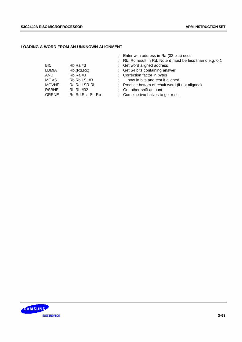
S3C2440A RISC MICROPROCESSOR ARM INSTRUCTION SET
3-63
LOADING A WORD FROM AN UNKNOWN ALIGNMENT
; Enter with address in Ra (32 bits) uses; Rb, Rc result in Rd. Note d must be less than c e.g. 0,1
BIC Rb,Ra,#3 ; Get word aligned addressLDMIA Rb,Rd,Rc ; Get 64 bits containing answerAND Rb,Ra,#3 ; Correction factor in bytesMOVS Rb,Rb,LSL#3 ; ...now in bits and test if alignedMOVNE Rd,Rd,LSR Rb ; Produce bottom of result word (if not aligned)RSBNE Rb,Rb,#32 ; Get other shift amountORRNE Rd,Rd,Rc,LSL Rb ; Combine two halves to get result

ARM INSTRUCTION SET S3C2440A RISC MICROPROCESSOR
3-64
NOTES
S3C2440A RISC MICROPROCESSOR THUMB INSTRUCTION SET
4-1
4 THUMB INSTRUCTION SET
THUMB INSTRUCTION SET FORMAT
The thumb instruction sets are 16-bit versions of ARM instruction sets (32-bit format). The ARM instructions arereduced to 16-bit versions.Thumb instructions, at the cost of versatile functions of the ARM instruction sets. Thethumb instructions are decompressed to the ARM instructions by the Thumb decompressor inside the ARM920Tcore.
As the Thumb instructions are compressed ARM instructions, the Thumb instructions have the 16-bit formatinstructions and have some restrictions. The restriction by 16-bit format is fully notified for using the Thumbinstructions.
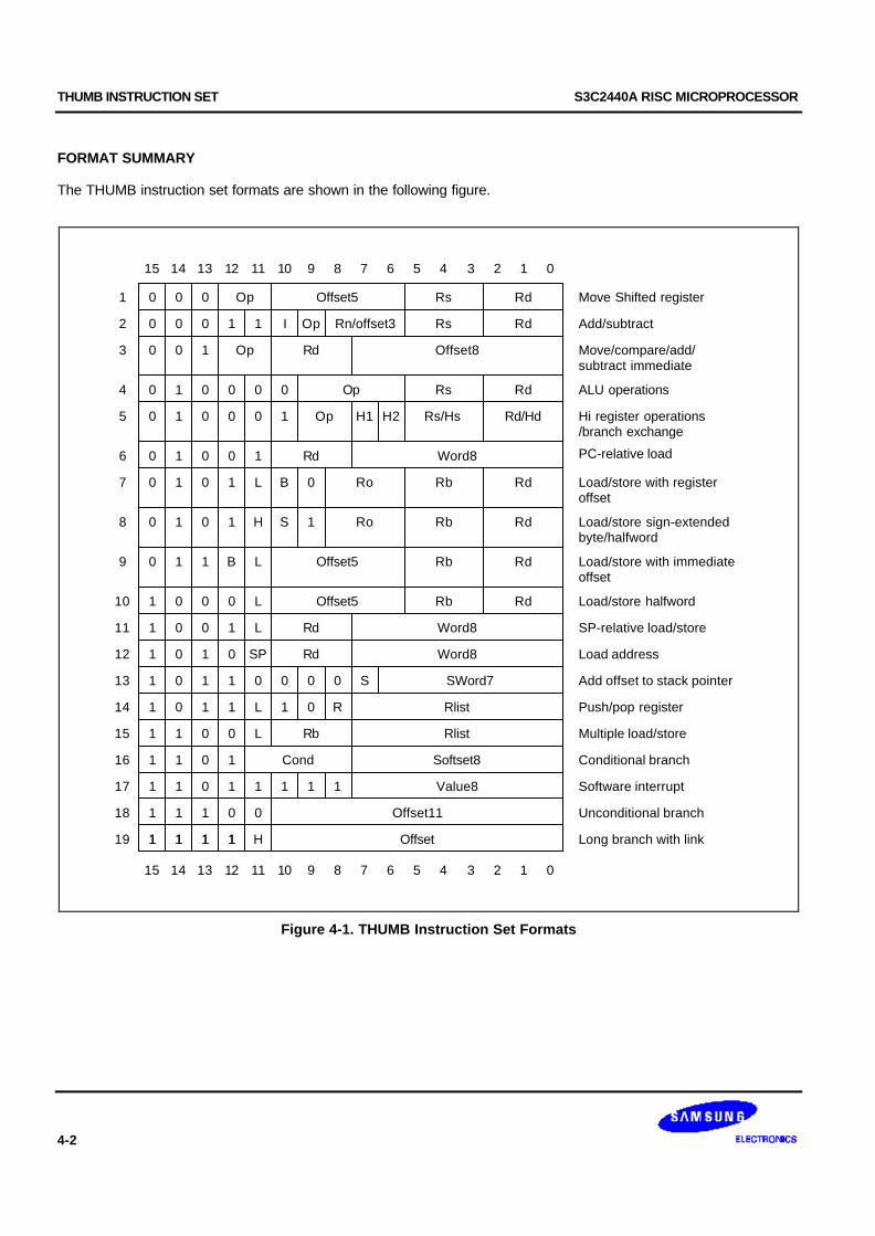
THUMB INSTRUCTION SET S3C2440A RISC MICROPROCESSOR
4-2
FORMAT SUMMARY
The THUMB instruction set formats are shown in the following figure.
Move Shifted register
00
0
0 0 0
0 0 0
0 0 0
1
0
0
0 1 0
0
0
0
0
0
1
11
1
1
1
1
00
0 0 0
1
1
1
1
11
1
1
0
L
0
1
1
1 1 1 1
1 1 1 1
1 1 1 1
1
1
0 0 0
0
1 1
1 1
0 0
10
0
L
1 0 R
1 1 0
1 0 SP
1 L
L
S
H
0
0
1 B L
0 1 H
0 1 B
0 0 1
1 1 I Op
Op
Op
Op
Op
L 0
S 1
Offset5 Rs Rd
Rn/offset3
Rd
Rs Rd
Offset8
Rs
Rd/Hd
Rd
H1 H2 Rs/Hs
Rd
Word8
Rd
RbRo
Ro Rb
Rd
Offset5 Rb Rd
Rb RdOffset5
Rd
Rd
Word8
Word8
SWord7
Rb
Cond
Rlist
Rlist
Softset8
Value8
Offset11
Offset
Add/subtract
Move/compare/add/subtract immediate
ALU operations
Hi register operations/branch exchange
PC-relative load
Load/store with registeroffset
Load/store with immediateoffset
Load/store sign-extendedbyte/halfword
Load/store halfword
SP-relative load/store
Load address
Add offset to stack pointer
Push/pop register
Multiple load/store
Conditional branch
Software interrupt
Unconditional branch
Long branch with link
15 14 13 12 11 10 9 8 7 6 5 4 23 1 0
15 14 13 12 11 10 9 8 7 6 5 4 23 1 0
1
2
3
4
5
6
7
8
9
10
11
12
13
14
15
16
17
18
19
Figure 4-1. THUMB Instruction Set Formats
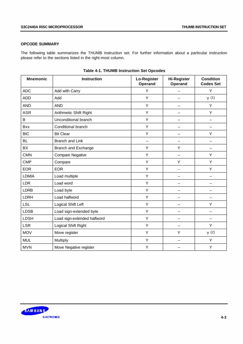
S3C2440A RISC MICROPROCESSOR THUMB INSTRUCTION SET
4-3
OPCODE SUMMARY
The following table summarizes the THUMB instruction set. For further information about a particular instructionplease refer to the sections listed in the right-most column.
Table 4-1. THUMB Instruction Set Opcodes
Mnemonic Instruction Lo-RegisterOperand
Hi-RegisterOperand
ConditionCodes Set
ADC Add with Carry Y – Y
ADD Add Y – Y (1)
AND AND Y – Y
ASR Arithmetic Shift Right Y – Y
B Unconditional branch Y – –
Bxx Conditional branch Y – –
BIC Bit Clear Y – Y
BL Branch and Link – – –
BX Branch and Exchange Y Y –
CMN Compare Negative Y – Y
CMP Compare Y Y Y
EOR EOR Y – Y
LDMIA Load multiple Y – –
LDR Load word Y – –
LDRB Load byte Y – –
LDRH Load halfword Y – –
LSL Logical Shift Left Y – Y
LDSB Load sign-extended byte Y – –
LDSH Load sign-extended halfword Y – –
LSR Logical Shift Right Y – Y
MOV Move register Y Y Y (2)
MUL Multiply Y – Y
MVN Move Negative register Y – Y
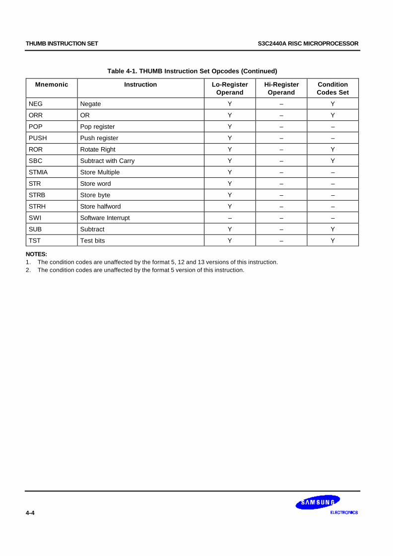
THUMB INSTRUCTION SET S3C2440A RISC MICROPROCESSOR
4-4
Table 4-1. THUMB Instruction Set Opcodes (Continued)
Mnemonic Instruction Lo-RegisterOperand
Hi-RegisterOperand
ConditionCodes Set
NEG Negate Y – Y
ORR OR Y – Y
POP Pop register Y – –
PUSH Push register Y – –
ROR Rotate Right Y – Y
SBC Subtract with Carry Y – Y
STMIA Store Multiple Y – –
STR Store word Y – –
STRB Store byte Y – –
STRH Store halfword Y – –
SWI Software Interrupt – – –
SUB Subtract Y – Y
TST Test bits Y – Y
NOTES:1. The condition codes are unaffected by the format 5, 12 and 13 versions of this instruction.2. The condition codes are unaffected by the format 5 version of this instruction.

S3C2440A RISC MICROPROCESSOR THUMB INSTRUCTION SET
4-5
FORMAT 1: MOVE SHIFTED REGISTER
15 0
0
14 10
[2:0] Destination Register
[5:3] Source Register [10:6] Immediate Vale
[12:11] Opcode0 = LSL1 = LSR2 = ASR
Offset5
6 5 3 2
Rd0 0
13 12 11
Op Rs
Figure 4-2. Format 1
OPERATION
These instructions move a shifted value between Lo registers. The THUMB assembler syntax is shown inTable 4-2.
NOTE
All instructions in this group set the CPSR condition codes.
Table 4-2. Summary of Format 1 Instructions
OP THUMB Assembler ARM Equipment Action
00 LSL Rd, Rs, #Offset5 MOVS Rd, Rs, LSL #Offset5 Shift Rs left by a 5-bit immediatevalue and store the result in Rd.
01 LSR Rd, Rs, #Offset5 MOVS Rd, Rs, LSR #Offset5 Perform logical shift right on Rs by a5-bit immediate value and store theresult in Rd.
10 ASR Rd, Rs, #Offset5 MOVS Rd, Rs, ASR #Offset5 Perform arithmetic shift right on Rsby a 5-bit immediate value and storethe result in Rd.
THUMB INSTRUCTION SET S3C2440A RISC MICROPROCESSOR
4-6
INSTRUCTION CYCLE TIMES
All instructions in this format have an equivalent ARM instruction as shown in Table 4-2. The instruction cycle timesfor the THUMB instruction are identical to that of the equivalent ARM instruction.
EXAMPLES
LSR R2, R5, #27 ; Logical shift right the contents of R5 by 27 and store the result in R2.Set condition codes on the result.
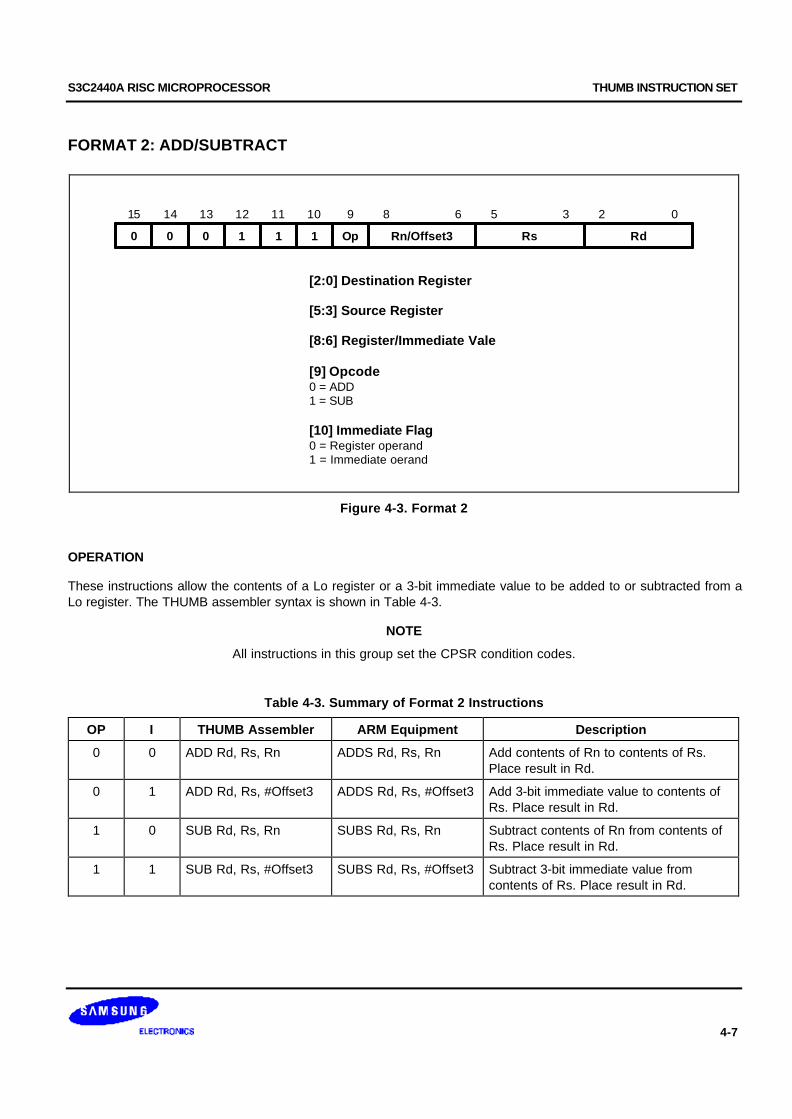
S3C2440A RISC MICROPROCESSOR THUMB INSTRUCTION SET
4-7
FORMAT 2: ADD/SUBTRACT
15
0
14 10
[2:0] Destination Register
[5:3] Source Register [8:6] Register/Immediate Vale
[9] Opcode0 = ADD1 = SUB
[10] Immediate Flag0 = Register operand1 = Immediate oerand
Rn/Offset3 Rd0 0
13 12 11
Op Rs
9 8
1 1 1
6 5 3 2 0
Figure 4-3. Format 2
OPERATION
These instructions allow the contents of a Lo register or a 3-bit immediate value to be added to or subtracted from aLo register. The THUMB assembler syntax is shown in Table 4-3.
NOTE
All instructions in this group set the CPSR condition codes.
Table 4-3. Summary of Format 2 Instructions
OP I THUMB Assembler ARM Equipment Description
0 0 ADD Rd, Rs, Rn ADDS Rd, Rs, Rn Add contents of Rn to contents of Rs.Place result in Rd.
0 1 ADD Rd, Rs, #Offset3 ADDS Rd, Rs, #Offset3 Add 3-bit immediate value to contents ofRs. Place result in Rd.
1 0 SUB Rd, Rs, Rn SUBS Rd, Rs, Rn Subtract contents of Rn from contents ofRs. Place result in Rd.
1 1 SUB Rd, Rs, #Offset3 SUBS Rd, Rs, #Offset3 Subtract 3-bit immediate value fromcontents of Rs. Place result in Rd.
THUMB INSTRUCTION SET S3C2440A RISC MICROPROCESSOR
4-8
INSTRUCTION CYCLE TIMES
All instructions in this format have an equivalent ARM instruction as shown in Table 4-3. The instruction cycle timesfor the THUMB instruction are identical to that of the equivalent ARM instruction.
EXAMPLES
ADD R0, R3, R4 ; R0 := R3 + R4 and set condition codes on the result.SUB R6, R2, #6 ; R6 := R2 - 6 and set condition codes.

S3C2440A RISC MICROPROCESSOR THUMB INSTRUCTION SET
4-9
FORMAT 3: MOVE/COMPARE/ADD/SUBTRACT IMMEDIATE
15 0
0
14 10
[7:0] Immediate Vale
[10:8] Source/Destination Register [12:11] Opcode0 = MOV1 = CMP2 = ADD3 = SUB
Offset8Rd0 0
13 12 11
Op
78
Figure 4-4. Format 3
OPERATIONS
The instructions in this group perform operations between a Lo register and an 8-bit immediate value. The THUMBassembler syntax is shown in Table 4-4.
NOTE
All instructions in this group set the CPSR condition codes.
Table 4-4. Summary of Format 3 Instructions
OP THUMB Assembler ARM Equipment Description
00 MOV Rd, #Offset8 MOVS Rd, #Offset8 Move 8-bit immediate value into Rd.
01 CMP Rd, #Offset8 CMP Rd, #Offset8 Compare contents of Rd with 8-bit immediatevalue.
10 ADD Rd, #Offset8 ADDS Rd, Rd, #Offset8 Add 8-bit immediate value to contents of Rdand place the result in Rd.
11 SUB Rd, #Offset8 SUBS Rd, Rd, #Offset8 Subtract 8-bit immediate value from contentsof Rd and place the result in Rd.

THUMB INSTRUCTION SET S3C2440A RISC MICROPROCESSOR
4-10
INSTRUCTION CYCLE TIMES
All instructions in this format have an equivalent ARM instruction as shown in Table 4-4. The instruction cycle timesfor the THUMB instruction are identical to that of the equivalent ARM instruction.
EXAMPLES
MOV R0, #128 ; R0 := 128 and set condition codesCMP R2, #62 ; Set condition codes on R2 - 62ADD R1, #255 ; R1 := R1 + 255 and set condition codesSUB R6, #145 ; R6 := R6 - 145 and set condition codes

S3C2440A RISC MICROPROCESSOR THUMB INSTRUCTION SET
4-11
FORMAT 4: ALU OPERATIONS
15 0
0
14 10
[2:0] Source/Destination Register
[5:3] Source Register 2 [9:6] Opcode
56 3
Rd0 0
13 12 11
Op Rs0 0 0
9 2
Figure 4-5. Format 4
OPERATION
The following instructions perform ALU operations on a Lo register pair.
NOTE
All instructions in this group set the CPSR condition codes.
Table 4-5. Summary of Format 4 Instructions
OP THUMB Assembler ARM Equipment Description
0000 AND Rd, Rs ANDS Rd, Rd, Rs Rd := Rd AND Rs
0001 EOR Rd, Rs EORS Rd, Rd, Rs Rd := Rd EOR Rs
0010 LSL Rd, Rs MOVS Rd, Rd, LSL Rs Rd := Rd << Rs
0011 LSR Rd, Rs MOVS Rd, Rd, LSR Rs Rd := Rd >> Rs
0100 ASR Rd, Rs MOVS Rd, Rd, ASR Rs Rd := Rd ASR Rs
0101 ADC Rd, Rs ADCS Rd, Rd, Rs Rd := Rd + Rs + C-bit
0110 SBC Rd, Rs SBCS Rd, Rd, Rs Rd := Rd - Rs - NOT C-bit
0111 ROR Rd, Rs MOVS Rd, Rd, ROR Rs Rd := Rd ROR Rs
1000 TST Rd, Rs TST Rd, Rs Set condition codes on Rd AND Rs
1001 NEG Rd, Rs RSBS Rd, Rs, #0 Rd = – Rs
1010 CMP Rd, Rs CMP Rd, Rs Set condition codes on Rd – Rs
1011 CMN Rd, Rs CMN Rd, Rs Set condition codes on Rd + Rs
1100 ORR Rd, Rs ORRS Rd, Rd, Rs Rd := Rd OR Rs
1101 MUL Rd, Rs MULS Rd, Rs, Rd Rd := Rs * Rd
1110 BIC Rd, Rs BICS Rd, Rd, Rs Rd := Rd AND NOT Rs
1111 MVN Rd, Rs MVNS Rd, Rs Rd := NOT Rs
THUMB INSTRUCTION SET S3C2440A RISC MICROPROCESSOR
4-12
INSTRUCTION CYCLE TIMES
All instructions in this format have an equivalent ARM instruction as shown in Table 4-5. The instruction cycle timesfor the THUMB instruction are identical to that of the equivalent ARM instruction.
EXAMPLES
EOR R3, R4 ; R3 := R3 EOR R4 and set condition codesROR R1, R0 ; Rotate Right R1 by the value in R0, store
; the result in R1 and set condition codesNEG R5, R3 ; Subtract the contents of R3 from zero,
; Store the result in R5. Set condition codes ie R5 = – R3CMP R2, R6 ; Set the condition codes on the result of R2 - R6MUL R0, R7 ; R0 := R7 × R0 and set condition codes
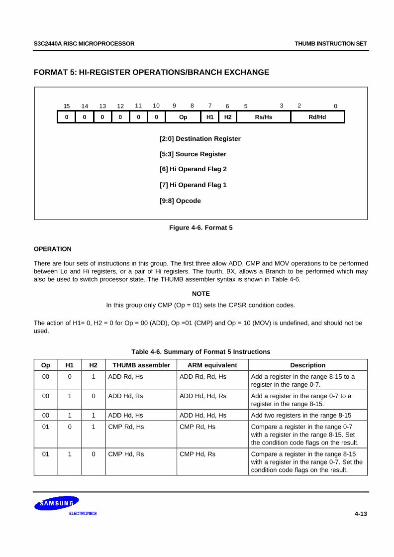
S3C2440A RISC MICROPROCESSOR THUMB INSTRUCTION SET
4-13
FORMAT 5: HI-REGISTER OPERATIONS/BRANCH EXCHANGE
15 0
0
14 10
[2:0] Destination Register
[5:3] Source Register [6] Hi Operand Flag 2
[7] Hi Operand Flag 1
[9:8] Opcode
6 5 3 2
Rd/Hd0 0
13 12 11
Op Rs/Hs0 0 0
9 8 7
H1 H2
Figure 4-6. Format 5
OPERATION
There are four sets of instructions in this group. The first three allow ADD, CMP and MOV operations to be performedbetween Lo and Hi registers, or a pair of Hi registers. The fourth, BX, allows a Branch to be performed which mayalso be used to switch processor state. The THUMB assembler syntax is shown in Table 4-6.
NOTE
In this group only CMP (Op = 01) sets the CPSR condition codes.
The action of H1= 0, H2 = 0 for Op = 00 (ADD), Op =01 (CMP) and Op = 10 (MOV) is undefined, and should not beused.
Table 4-6. Summary of Format 5 Instructions
Op H1 H2 THUMB assembler ARM equivalent Description
00 0 1 ADD Rd, Hs ADD Rd, Rd, Hs Add a register in the range 8-15 to aregister in the range 0-7.
00 1 0 ADD Hd, Rs ADD Hd, Hd, Rs Add a register in the range 0-7 to aregister in the range 8-15.
00 1 1 ADD Hd, Hs ADD Hd, Hd, Hs Add two registers in the range 8-15
01 0 1 CMP Rd, Hs CMP Rd, Hs Compare a register in the range 0-7with a register in the range 8-15. Setthe condition code flags on the result.
01 1 0 CMP Hd, Rs CMP Hd, Rs Compare a register in the range 8-15with a register in the range 0-7. Set thecondition code flags on the result.
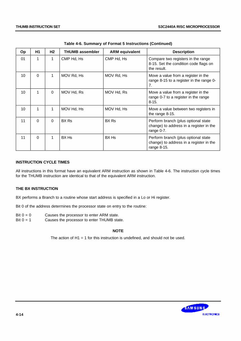
THUMB INSTRUCTION SET S3C2440A RISC MICROPROCESSOR
4-14
Table 4-6. Summary of Format 5 Instructions (Continued)
Op H1 H2 THUMB assembler ARM equivalent Description
01 1 1 CMP Hd, Hs CMP Hd, Hs Compare two registers in the range8-15. Set the condition code flags onthe result.
10 0 1 MOV Rd, Hs MOV Rd, Hs Move a value from a register in therange 8-15 to a register in the range 0-7.
10 1 0 MOV Hd, Rs MOV Hd, Rs Move a value from a register in therange 0-7 to a register in the range8-15.
10 1 1 MOV Hd, Hs MOV Hd, Hs Move a value between two registers inthe range 8-15.
11 0 0 BX Rs BX Rs Perform branch (plus optional statechange) to address in a register in therange 0-7.
11 0 1 BX Hs BX Hs Perform branch (plus optional statechange) to address in a register in therange 8-15.
INSTRUCTION CYCLE TIMES
All instructions in this format have an equivalent ARM instruction as shown in Table 4-6. The instruction cycle timesfor the THUMB instruction are identical to that of the equivalent ARM instruction.
THE BX INSTRUCTION
BX performs a Branch to a routine whose start address is specified in a Lo or Hi register.
Bit 0 of the address determines the processor state on entry to the routine:
Bit 0 = 0 Causes the processor to enter ARM state.Bit 0 = 1 Causes the processor to enter THUMB state.
NOTE
The action of H1 = 1 for this instruction is undefined, and should not be used.

S3C2440A RISC MICROPROCESSOR THUMB INSTRUCTION SET
4-15
EXAMPLES
Hi-Register Operations
ADD PC, R5 ; PC := PC + R5 but don't set the condition codes.CMP R4, R12 ; Set the condition codes on the result of R4 - R12.MOV R15, R14 ; Move R14 (LR) into R15 (PC) but don't set the condition
codes, eg. return from subroutine.
Branch and Exchange
; Switch from THUMB to ARM state.ADR R1,outofTHUMB ; Load address of outofTHUMB into R1.MOV R11,R1BX R11 ; Transfer the contents of R11 into the PC.
; Bit 0 of R11 determines whether; ARM or THUMB state is entered, ie. In this case the
state is ARM.
ALIGNCODE32outofTHUMB ; Now processing ARM instructions...
USING R15 AS AN OPERAND
If R15 is used as an operand, the value will be the address of the instruction + 4 with bit 0 cleared. Executing a BXPC in THUMB state from a non-word aligned address will result in unpredictable execution.
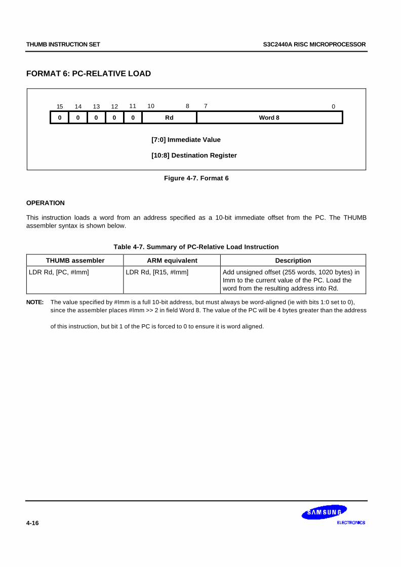
THUMB INSTRUCTION SET S3C2440A RISC MICROPROCESSOR
4-16
FORMAT 6: PC-RELATIVE LOAD
15 0
0
14 10
[7:0] Immediate Value
[10:8] Destination Register
Word 80 0
13 12 11
Rd0 0
8 7
Figure 4-7. Format 6
OPERATION
This instruction loads a word from an address specified as a 10-bit immediate offset from the PC. The THUMBassembler syntax is shown below.
Table 4-7. Summary of PC-Relative Load Instruction
THUMB assembler ARM equivalent Description
LDR Rd, [PC, #Imm] LDR Rd, [R15, #Imm] Add unsigned offset (255 words, 1020 bytes) inImm to the current value of the PC. Load theword from the resulting address into Rd.
NOTE: The value specified by #Imm is a full 10-bit address, but must always be word-aligned (ie with bits 1:0 set to 0), since the assembler places #Imm >> 2 in field Word 8. The value of the PC will be 4 bytes greater than the address
of this instruction, but bit 1 of the PC is forced to 0 to ensure it is word aligned.

S3C2440A RISC MICROPROCESSOR THUMB INSTRUCTION SET
4-17
INSTRUCTION CYCLE TIMES
All instructions in this format have an equivalent ARM instruction. The instruction cycle times for the THUMBinstruction are identical to that of the equivalent ARM instruction.
EXAMPLES
LDR R3,[PC,#844] ; Load into R3 the word found at the addressformed by adding 844 to PC.bit[1] of PC is forced to zero.
Note that the THUMB opcode will contain 211 as theWord8 value.
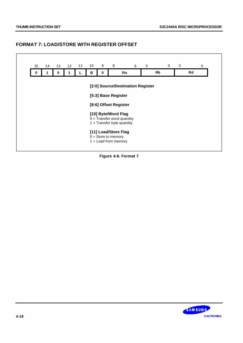
THUMB INSTRUCTION SET S3C2440A RISC MICROPROCESSOR
4-18
FORMAT 7: LOAD/STORE WITH REGISTER OFFSET
[2:0] Source/Destination Register
[5:3] Base Register [8:6] Offset Register
[10] Byte/Word Flag0 = Transfer word quantity1 = Transfer byte quantity
[11] Load/Store Flag0 = Store to memory1 = Load from memory
15 0
0
14 10 6 5 3 2
Rd1 0
13 12 11
Rb1 L B
9 8
Ro0
Figure 4-8. Format 7
S3C2440A RISC MICROPROCESSOR THUMB INSTRUCTION SET
4-19
OPERATION
These instructions transfer byte or word values between registers and memory. Memory addresses are pre-indexedusing an offset register in the range 0-7. The THUMB assembler syntax is shown in Table 4-8.
Table 4-8. Summary of Format 7 Instructions
L B THUMB assembler ARM equivalent Description
0 0 STR Rd, [Rb, Ro] STR Rd, [Rb, Ro] Pre-indexed word store:Calculate the target address by addingtogether the value in Rb and the value inRo. Store the contents of Rd at theaddress.
0 1 STRB Rd, [Rb, Ro] STRB Rd, [Rb, Ro] Pre-indexed byte store:Calculate the target address by addingtogether the value in Rb and the value inRo. Store the byte value in Rd at theresulting address.
1 0 LDR Rd, [Rb, Ro] LDR Rd, [Rb, Ro] Pre-indexed word load:Calculate the source address by addingtogether the value in Rb and the value inRo. Load the contents of the address intoRd.
1 1 LDRB Rd, [Rb, Ro] LDRB Rd, [Rb, Ro] Pre-indexed byte load:Calculate the source address by addingtogether the value in Rb and the value inRo. Load the byte value at the resultingaddress.
INSTRUCTION CYCLE TIMES
All instructions in this format have an equivalent ARM instruction as shown in Table 4-8. The instruction cycle timesfor the THUMB instruction are identical to that of the equivalent ARM instruction.
EXAMPLES
STR R3, [R2,R6] ; Store word in R3 at the address formed by adding R6 to R2.
LDRB R2, [R0,R7] ; Load into R2 the byte found at the address formed by adding R7 to R0.

THUMB INSTRUCTION SET S3C2440A RISC MICROPROCESSOR
4-20
FORMAT 8: LOAD/STORE SIGN-EXTENDED BYTE/HALFWORD
[2:0] Destination Register
[5:3] Base Register [8:6] Offset Register
[10] Sign-Extended Flag0 = Operand not sing-extended1 = Operand sing-extended
[11] H Flag
15 0
0
14 10 6 5 3 2
Rd1 0
13 12 11
Rb1 H S
9 8
Ro1
Figure 4-9. Format 8
OPERATION
These instructions load optionally sign-extended bytes or halfwords, and store halfwords. The THUMB assemblersyntax is shown below.
Table 4-9. Summary of Format 8 Instructions
L B THUMB assembler ARM equivalent Description
0 0 STRH Rd, [Rb, Ro] STRH Rd, [Rb, Ro] Store halfword:
Add Ro to base address in Rb. Store bits0-15 of Rd at the resulting address.
0 1 LDRH Rd, [Rb, Ro] LDRH Rd, [Rb, Ro] Load halfword:
Add Ro to base address in Rb. Load bits0-15 of Rd from the resulting address, andset bits 16-31 of Rd to 0.
1 0 LDSB Rd, [Rb, Ro] LDRSB Rd, [Rb, Ro] Load sign-extended byte:
Add Ro to base address in Rb. Load bits0-7 of Rd from the resulting address, andset bits 8-31 of Rd to bit 7.
1 1 LDSH Rd, [Rb, Ro] LDRSH Rd, [Rb, Ro] Load sign-extended halfword:
Add Ro to base address in Rb. Load bits0-15 of Rd from the resulting address, andset bits 16-31 of Rd to bit 15.
S3C2440A RISC MICROPROCESSOR THUMB INSTRUCTION SET
4-21
INSTRUCTION CYCLE TIMES
All instructions in this format have an equivalent ARM instruction as shown in Table 4-9. The instruction cycle timesfor the THUMB instruction are identical to that of the equivalent ARM instruction.
EXAMPLES
STRH R4, [R3, R0] ; Store the lower 16 bits of R4 at the address formed by adding R0 to R3.
LDSB R2, [R7, R1] ; Load into R2 the sign extended byte found at the addressformed by adding R1 to R7.
LDSH R3, [R4, R2] ; Load into R3 the sign extended halfword found at theaddress formed by adding R2 to R4.

THUMB INSTRUCTION SET S3C2440A RISC MICROPROCESSOR
4-22
FORMAT 9: LOAD/STORE WITH IMMEDIATE OFFSET
[2:0] Source/Destination Register
[5:3] Base Register [10:6] Offset Register
[11] Load/Store Flag0 = Store to memory1 = Load from memory
[12] Byte/Word Flad0 = Transfer word quantity1 = Transfer byte quantity
15 0
0
14 10 6 5 3 2
Rd1 1
13 12 11
RbB L Offset5
Figure 4-10. Format 9

S3C2440A RISC MICROPROCESSOR THUMB INSTRUCTION SET
4-23
OPERATION
These instructions transfer byte or word values between registers and memory using an immediate 5 or 7-bit offset.The THUMB assembler syntax is shown in Table 4-10.
Table 4-10. Summary of Format 9 Instructions
L B THUMB assembler ARM equivalent Description
0 0 STR Rd, [Rb, #Imm] STR Rd, [Rb, #Imm] Calculate the target address by addingtogether the value in Rb and Imm. Storethe contents of Rd at the address.
1 0 LDR Rd, [Rb, #Imm] LDR Rd, [Rb, #Imm] Calculate the source address by addingtogether the value in Rb and Imm. LoadRd from the address.
0 1 STRB Rd, [Rb, #Imm] STRB Rd, [Rb, #Imm] Calculate the target address by addingtogether the value in Rb and Imm. Storethe byte value in Rd at the address.
1 1 LDRB Rd, [Rb, #Imm] LDRB Rd, [Rb, #Imm] Calculate source address by addingtogether the value in Rb and Imm. Loadthe byte value at the address into Rd.
NOTE: For word accesses (B = 0), the value specified by #Imm is a full 7-bit address, but must be word-aligned(ie with bits 1:0 set to 0), since the assembler places #Imm >> 2 in the Offset5 field.
INSTRUCTION CYCLE TIMES
All instructions in this format have an equivalent ARM instruction as shown in Table 4-10. The instruction cycle timesfor the THUMB instruction are identical to that of the equivalent ARM instruction.
EXAMPLES
LDR R2, [R5,#116] ; Load into R2 the word found at the address formed by adding 116 to R5.Note that the THUMB opcode will contain 29 as the Offset5 value.
STRB R1, [R0,#13] ; Store the lower 8 bits of R1 at the address formed by adding 13 to R0.Note that the THUMB opcode will contain 13 as the Offset5 value.

THUMB INSTRUCTION SET S3C2440A RISC MICROPROCESSOR
4-24
FORMAT 10: LOAD/STORE HALFWORD
[2:0] Source/Destination Register
[5:3] Base Register [10:6] Immediate Value
[11] Load/Store Flag0 = Store to memory1 = Load from memory
15 0
0
14 10 6 5 3 2
Rd1 0
13 12 11
Rb0 L Offset5
Figure 4-11. Format 10
OPERATION
These instructions transfer halfword values between a Lo register and memory. Addresses are pre-indexed, using a6-bit immediate value. The THUMB assembler syntax is shown in Table 4-11.
Table 4-11. Halfword Data Transfer Instructions
L THUMB assembler ARM equivalent Description
0 STRH Rd, [Rb, #Imm] STRH Rd, [Rb, #Imm] Add #Imm to base address in Rb and storebits 0 - 15 of Rd at the resulting address.
1 LDRH Rd, [Rb, #Imm] LDRH Rd, [Rb, #Imm] Add #Imm to base address in Rb. Load bits0-15 from the resulting address into Rd andset bits 16-31 to zero.
NOTE: #Imm is a full 6-bit address but must be halfword-aligned (ie with bit 0 set to 0) since the assembler places#Imm >> 1 in the Offset5 field.

S3C2440A RISC MICROPROCESSOR THUMB INSTRUCTION SET
4-25
INSTRUCTION CYCLE TIMES
All instructions in this format have an equivalent ARM instruction as shown in Table 4-11. The instruction cycle timesfor the THUMB instruction are identical to that of the equivalent ARM instruction.
EXAMPLES
STRH R6, [R1, #56] ; Store the lower 16 bits of R4 at the address formed byadding 56 R1. Note that the THUMB opcode will contain 28 as the Offset5 value.
LDRH R4, [R7, #4] ; Load into R4 the halfword found at the address formed by adding 4 to R7. Note that the THUMB opcode will contain 2 as the Offset5 value.

THUMB INSTRUCTION SET S3C2440A RISC MICROPROCESSOR
4-26
FORMAT 11: SP-RELATIVE LOAD/STORE
[7:0] Immediate Value
[10:8] Destination Register [11] Load/Store Bit0 = Store to memory1 = Load from memory
15 0
1
14 10
0 0
13 12 11
Word 81 L Rd
78
Figure 4-12. Format 11
OPERATION
The instructions in this group perform an SP-relative load or store. The THUMB assembler syntax is shown in thefollowing table.
Table 4-12. SP-Relative Load/Store Instructions
L THUMB assembler ARM equivalent Description
0 STR Rd, [SP, #Imm] STR Rd, [R13 #Imm] Add unsigned offset (255 words, 1020 bytes)in Imm to the current value of the SP (R7).Store the contents of Rd at the resultingaddress.
1 LDR Rd, [SP, #Imm] LDR Rd, [R13 #Imm] Add unsigned offset (255 words, 1020 bytes)in Imm to the current value of the SP (R7).Load the word from the resulting address intoRd.
NOTE: The offset supplied in #Imm is a full 10-bit address, but must always be word-aligned (ie bits 1:0 set to 0),since the assembler places #Imm >> 2 in the Word8 field.
S3C2440A RISC MICROPROCESSOR THUMB INSTRUCTION SET
4-27
INSTRUCTION CYCLE TIMES
All instructions in this format have an equivalent ARM instruction as shown in Table 4-12. The instruction cycle timesfor the THUMB instruction are identical to that of the equivalent ARM instruction.
EXAMPLES
STR R4, [SP,#492] ; Store the contents of R4 at the address formed by adding 492 to SP (R13).Note that the THUMB opcode will contain 123 as the Word8 value.

THUMB INSTRUCTION SET S3C2440A RISC MICROPROCESSOR
4-28
FORMAT 12: LOAD ADDRESS
[7:0] 8-bit Unsigned Constant
[10:8] Destination Register [11] Source0 = PC1 = SP
15 0
1
14 10
0 1
13 12 11
Word 80 SP Rd
78
Figure 4-13. Format 12
OPERATION
These instructions calculate an address by adding a 10-bit constant to either the PC or the SP, and load theresulting address into a register. The THUMB assembler syntax is shown in the following table.
Table 4-13. Load Address
L THUMB assembler ARM equivalent Description
0 ADD Rd, PC, #Imm ADD Rd, R15, #Imm Add #Imm to the current value of the programcounter (PC) and load the result into Rd.
1 ADD Rd, SP, #Imm ADD Rd, R13, #Imm Add #Imm to the current value of the stackpointer (SP) and load the result into Rd.
NOTE: The value specified by #Imm is a full 10-bit value, but this must be word-aligned (ie with bits 1:0 set to 0)since the assembler places #Imm >> 2 in field Word 8.
Where the PC is used as the source register (SP = 0), bit 1 of the PC is always read as 0. The value of the PC willbe 4 bytes greater than the address of the instruction before bit 1 is forced to 0.
The CPSR condition codes are unaffected by these instructions.

S3C2440A RISC MICROPROCESSOR THUMB INSTRUCTION SET
4-29
INSTRUCTION CYCLE TIMES
All instructions in this format have an equivalent ARM instruction as shown in Table 4-13. The instruction cycle timesfor the THUMB instruction are identical to that of the equivalent ARM instruction.
EXAMPLES
ADD R2, PC, #572 ; R2 := PC + 572, but don't set thecondition codes. bit[1] of PC is forced to zero.Note that the THUMB opcode willcontain 143 as the Word8 value.
ADD R6, SP, #212 ; R6 := SP (R13) + 212, but don'tset the condition codes. Note that the THUMB opcode will contain 53 as the
Word 8 value.
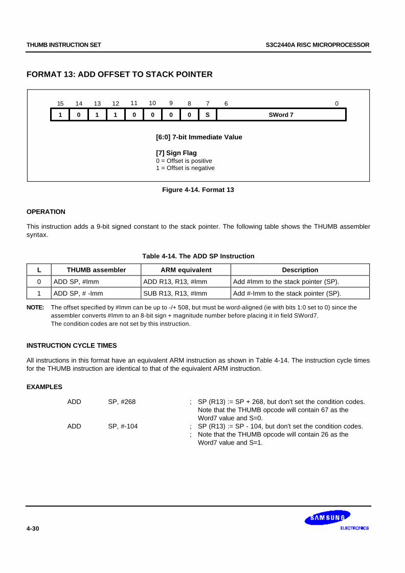
THUMB INSTRUCTION SET S3C2440A RISC MICROPROCESSOR
4-30
FORMAT 13: ADD OFFSET TO STACK POINTER
[6:0] 7-bit Immediate Value
[7] Sign Flag0 = Offset is positive1 = Offset is negative
15 0
1
14 10
0 1
13 12 11
SWord 71 0 0
789 6
0 0 S
Figure 4-14. Format 13
OPERATION
This instruction adds a 9-bit signed constant to the stack pointer. The following table shows the THUMB assemblersyntax.
Table 4-14. The ADD SP Instruction
L THUMB assembler ARM equivalent Description
0 ADD SP, #Imm ADD R13, R13, #Imm Add #Imm to the stack pointer (SP).
1 ADD SP, # -Imm SUB R13, R13, #Imm Add #-Imm to the stack pointer (SP).
NOTE: The offset specified by #Imm can be up to -/+ 508, but must be word-aligned (ie with bits 1:0 set to 0) since the assembler converts #Imm to an 8-bit sign + magnitude number before placing it in field SWord7. The condition codes are not set by this instruction.
INSTRUCTION CYCLE TIMES
All instructions in this format have an equivalent ARM instruction as shown in Table 4-14. The instruction cycle timesfor the THUMB instruction are identical to that of the equivalent ARM instruction.
EXAMPLES
ADD SP, #268 ; SP (R13) := SP + 268, but don't set the condition codes. Note that the THUMB opcode will contain 67 as the Word7 value and S=0.
ADD SP, #-104 ; SP (R13) := SP - 104, but don't set the condition codes.; Note that the THUMB opcode will contain 26 as the
Word7 value and S=1.

S3C2440A RISC MICROPROCESSOR THUMB INSTRUCTION SET
4-31
FORMAT 14: PUSH/POP REGISTERS
[7:0] Register List
[8] PC/LR Bit0 = Do not store LR/Load PC1 = Store LR/Load PC
[11] Load/Store Bit0 = Store to memory1 = Load from memory
15 0
1
14 10
0 1
13 12 11
Rlist1 L 0
789
1 R
Figure 4-15. Format 14
OPERATION
The instructions in this group allow registers 0-7 and optionally LR to be pushed onto the stack, and registers 0-7and optionally PC to be popped off the stack. The THUMB assembler syntax is shown in Table 4-15.
NOTE
The stack is always assumed to be Full Descending.
Table 4-15. PUSH and POP Instructions
L B THUMB assembler ARM equivalent Description
0 0 PUSH Rlist STMDB R13!, Rlist Push the registers specified by Rlist ontothe stack. Update the stack pointer.
0 1 PUSH Rlist, LR STMDB R13!, Rlist, R14
Push the Link Register and the registersspecified by Rlist (if any) onto the stack.Update the stack pointer.
1 0 POP Rlist LDMIA R13!, Rlist Pop values off the stack into the registersspecified by Rlist. Update the stackpointer.
1 1 POP Rlist, PC LDMIA R13!, Rlist, R15 Pop values off the stack and load into theregisters specified by Rlist. Pop the PC offthe stack. Update the stack pointer.
THUMB INSTRUCTION SET S3C2440A RISC MICROPROCESSOR
4-32
INSTRUCTION CYCLE TIMES
All instructions in this format have an equivalent ARM instruction as shown in Table 4-15. The instruction cycle timesfor the THUMB instruction are identical to that of the equivalent ARM instruction.
EXAMPLES
PUSH R0-R4,LR ; Store R0,R1,R2,R3,R4 and R14 (LR) at the stack pointed to by R13 (SP) and update R13.
Useful at start of a sub-routine to save workspace and return address.
POP R2,R6,PC ; Load R2,R6 and R15 (PC) from the stack pointed to by R13 (SP) and update R13.Useful to restore workspace and return from sub-routine.
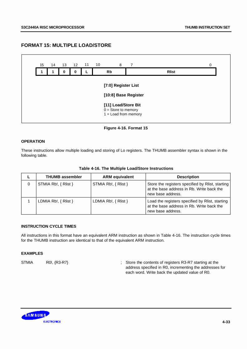
S3C2440A RISC MICROPROCESSOR THUMB INSTRUCTION SET
4-33
FORMAT 15: MULTIPLE LOAD/STORE
[7:0] Register List
[10:8] Base Register
[11] Load/Store Bit0 = Store to memory1 = Load from memory
15 0
1
14 10
1 0
13 12 11
Rlist0 L
78
Rb
Figure 4-16. Format 15
OPERATION
These instructions allow multiple loading and storing of Lo registers. The THUMB assembler syntax is shown in thefollowing table.
Table 4-16. The Multiple Load/Store Instructions
L THUMB assembler ARM equivalent Description
0 STMIA Rb!, Rlist STMIA Rb!, Rlist Store the registers specified by Rlist, startingat the base address in Rb. Write back thenew base address.
1 LDMIA Rb!, Rlist LDMIA Rb!, Rlist Load the registers specified by Rlist, startingat the base address in Rb. Write back thenew base address.
INSTRUCTION CYCLE TIMES
All instructions in this format have an equivalent ARM instruction as shown in Table 4-16. The instruction cycle timesfor the THUMB instruction are identical to that of the equivalent ARM instruction.
EXAMPLES
STMIA R0!, R3-R7 ; Store the contents of registers R3-R7 starting at the address specified in R0, incrementing the addresses for each word. Write back the updated value of R0.
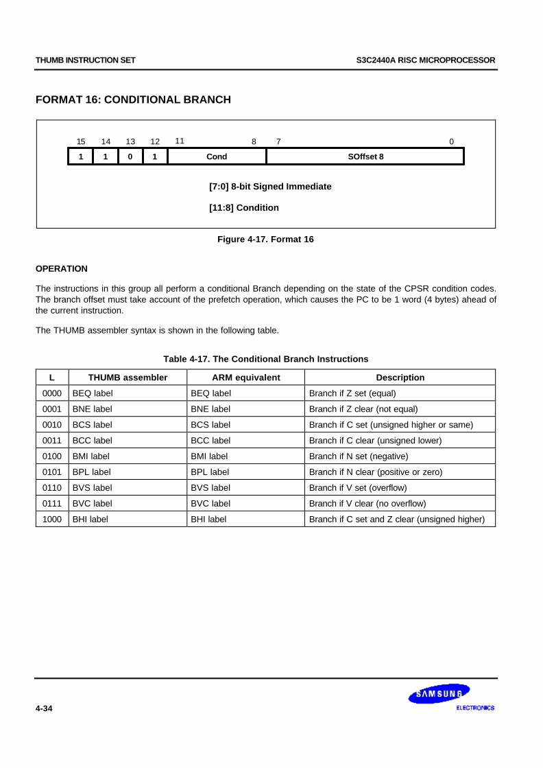
THUMB INSTRUCTION SET S3C2440A RISC MICROPROCESSOR
4-34
FORMAT 16: CONDITIONAL BRANCH
[7:0] 8-bit Signed Immediate
[11:8] Condition
15 0
1
14
1 0
13 12 11
SOffset 81
78
Cond
Figure 4-17. Format 16
OPERATION
The instructions in this group all perform a conditional Branch depending on the state of the CPSR condition codes.The branch offset must take account of the prefetch operation, which causes the PC to be 1 word (4 bytes) ahead ofthe current instruction.
The THUMB assembler syntax is shown in the following table.
Table 4-17. The Conditional Branch Instructions
L THUMB assembler ARM equivalent Description
0000 BEQ label BEQ label Branch if Z set (equal)
0001 BNE label BNE label Branch if Z clear (not equal)
0010 BCS label BCS label Branch if C set (unsigned higher or same)
0011 BCC label BCC label Branch if C clear (unsigned lower)
0100 BMI label BMI label Branch if N set (negative)
0101 BPL label BPL label Branch if N clear (positive or zero)
0110 BVS label BVS label Branch if V set (overflow)
0111 BVC label BVC label Branch if V clear (no overflow)
1000 BHI label BHI label Branch if C set and Z clear (unsigned higher)
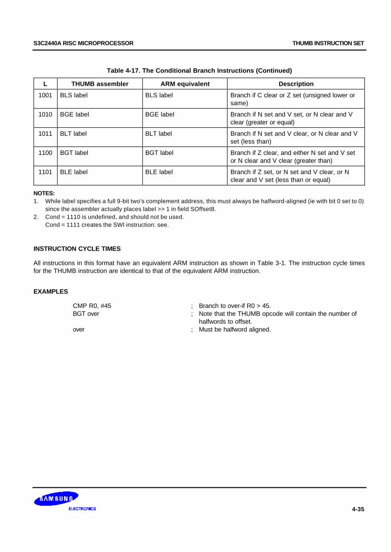
S3C2440A RISC MICROPROCESSOR THUMB INSTRUCTION SET
4-35
Table 4-17. The Conditional Branch Instructions (Continued)
L THUMB assembler ARM equivalent Description
1001 BLS label BLS label Branch if C clear or Z set (unsigned lower orsame)
1010 BGE label BGE label Branch if N set and V set, or N clear and Vclear (greater or equal)
1011 BLT label BLT label Branch if N set and V clear, or N clear and Vset (less than)
1100 BGT label BGT label Branch if Z clear, and either N set and V setor N clear and V clear (greater than)
1101 BLE label BLE label Branch if Z set, or N set and V clear, or Nclear and V set (less than or equal)
NOTES:1. While label specifies a full 9-bit two's complement address, this must always be halfword-aligned (ie with bit 0 set to 0)
since the assembler actually places label >> 1 in field SOffset8.2. Cond = 1110 is undefined, and should not be used.
Cond = 1111 creates the SWI instruction: see.
INSTRUCTION CYCLE TIMES
All instructions in this format have an equivalent ARM instruction as shown in Table 3-1. The instruction cycle timesfor the THUMB instruction are identical to that of the equivalent ARM instruction.
EXAMPLES
CMP R0, #45 ; Branch to over-if R0 > 45.BGT over ; Note that the THUMB opcode will contain the number of
halfwords to offset.over ; Must be halfword aligned.
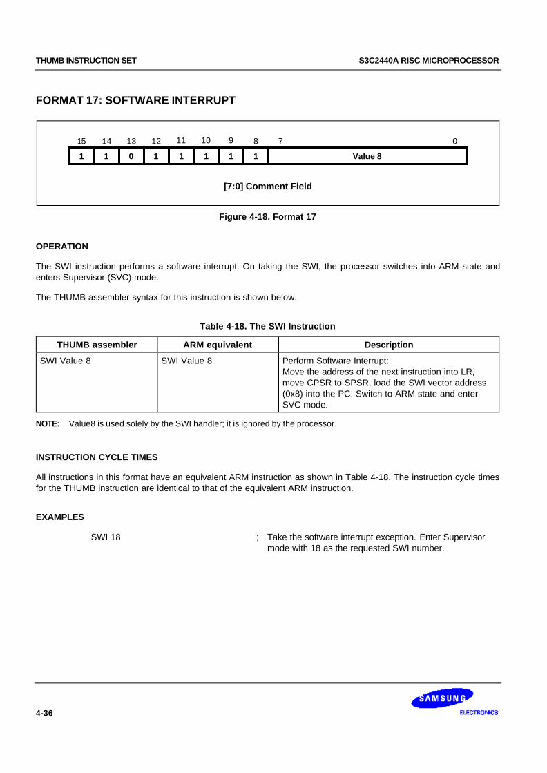
THUMB INSTRUCTION SET S3C2440A RISC MICROPROCESSOR
4-36
FORMAT 17: SOFTWARE INTERRUPT
[7:0] Comment Field
15 0
1
14
1 0
13 12 11
Value 81
7810 9
1 1 1 1
Figure 4-18. Format 17
OPERATION
The SWI instruction performs a software interrupt. On taking the SWI, the processor switches into ARM state andenters Supervisor (SVC) mode.
The THUMB assembler syntax for this instruction is shown below.
Table 4-18. The SWI Instruction
THUMB assembler ARM equivalent Description
SWI Value 8 SWI Value 8 Perform Software Interrupt:Move the address of the next instruction into LR,move CPSR to SPSR, load the SWI vector address(0x8) into the PC. Switch to ARM state and enterSVC mode.
NOTE: Value8 is used solely by the SWI handler; it is ignored by the processor.
INSTRUCTION CYCLE TIMES
All instructions in this format have an equivalent ARM instruction as shown in Table 4-18. The instruction cycle timesfor the THUMB instruction are identical to that of the equivalent ARM instruction.
EXAMPLES
SWI 18 ; Take the software interrupt exception. Enter Supervisormode with 18 as the requested SWI number.
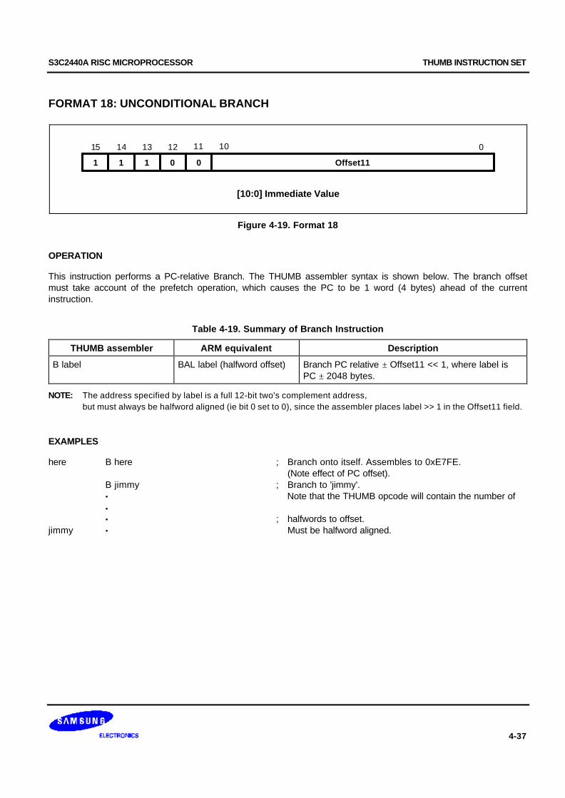
S3C2440A RISC MICROPROCESSOR THUMB INSTRUCTION SET
4-37
FORMAT 18: UNCONDITIONAL BRANCH
[10:0] Immediate Value
15 0
1
14
1 1
13 12 11
Offset110
10
0
Figure 4-19. Format 18
OPERATION
This instruction performs a PC-relative Branch. The THUMB assembler syntax is shown below. The branch offsetmust take account of the prefetch operation, which causes the PC to be 1 word (4 bytes) ahead of the currentinstruction.
Table 4-19. Summary of Branch Instruction
THUMB assembler ARM equivalent Description
B label BAL label (halfword offset) Branch PC relative ± Offset11 << 1, where label isPC ± 2048 bytes.
NOTE: The address specified by label is a full 12-bit two's complement address,but must always be halfword aligned (ie bit 0 set to 0), since the assembler places label >> 1 in the Offset11 field.
EXAMPLES
here B here ; Branch onto itself. Assembles to 0xE7FE. (Note effect of PC offset).
B jimmy ; Branch to 'jimmy'.• Note that the THUMB opcode will contain the number of •• ; halfwords to offset.
jimmy • Must be halfword aligned.

THUMB INSTRUCTION SET S3C2440A RISC MICROPROCESSOR
4-38
FORMAT 19: LONG BRANCH WITH LINK
[10:0] Long Branch and Link Offset High/Low
[11] Low/High Offset Bit0 = Offset high1 = Offset low
15 0
1
14
1 1
13 12 11
Offset1
10
H
Figure 4-20. Format 19
OPERATION
This format specifies a long branch with link.
The assembler splits the 23-bit two's complement half-word offset specified by the label into two 11-bit halves,ignoring bit 0 (which must be 0), and creates two THUMB instructions.
Instruction 1 (H = 0)
In the first instruction the Offset field contains the upper 11 bits of the target address. This is shifted left by 12 bitsand added to the current PC address. The resulting address is placed in LR.
Instruction 2 (H =1)
In the second instruction the Offset field contains an 11-bit representation lower half of the target address. This isshifted left by 1 bit and added to LR. LR, which now contains the full 23-bit address, is placed in PC, the address ofthe instruction following the BL is placed in LR and bit 0 of LR is set.
The branch offset must take account of the prefetch operation, which causes the PC to be 1 word (4 bytes) ahead ofthe current instruction
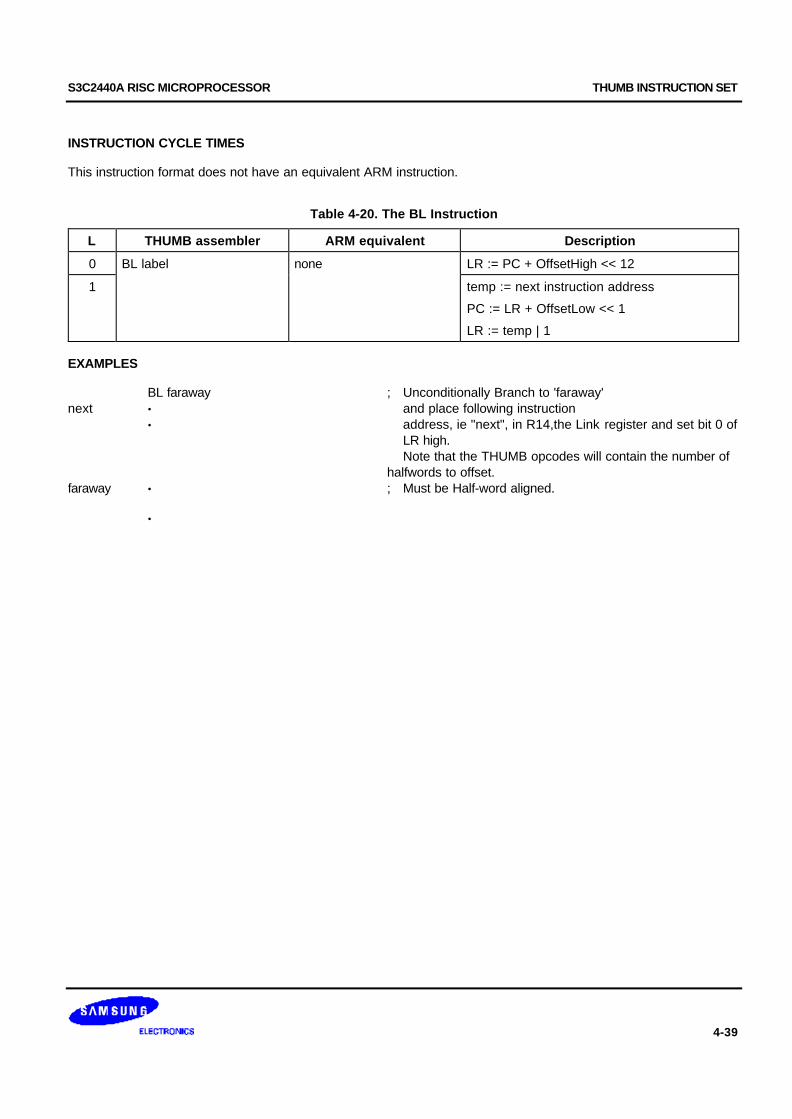
S3C2440A RISC MICROPROCESSOR THUMB INSTRUCTION SET
4-39
INSTRUCTION CYCLE TIMES
This instruction format does not have an equivalent ARM instruction.
Table 4-20. The BL Instruction
L THUMB assembler ARM equivalent Description
0 BL label none LR := PC + OffsetHigh << 12
1 temp := next instruction address
PC := LR + OffsetLow << 1
LR := temp | 1
EXAMPLES
BL faraway ; Unconditionally Branch to 'faraway'next • and place following instruction
• address, ie "next", in R14,the Link register and set bit 0 ofLR high.
Note that the THUMB opcodes will contain the number of halfwords to offset.
faraway • ; Must be Half-word aligned.
•
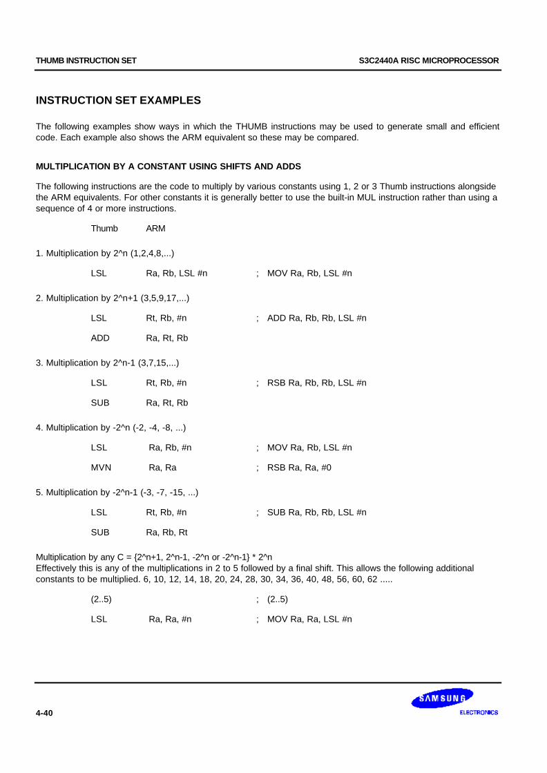
THUMB INSTRUCTION SET S3C2440A RISC MICROPROCESSOR
4-40
INSTRUCTION SET EXAMPLES
The following examples show ways in which the THUMB instructions may be used to generate small and efficientcode. Each example also shows the ARM equivalent so these may be compared.
MULTIPLICATION BY A CONSTANT USING SHIFTS AND ADDS
The following instructions are the code to multiply by various constants using 1, 2 or 3 Thumb instructions alongsidethe ARM equivalents. For other constants it is generally better to use the built-in MUL instruction rather than using asequence of 4 or more instructions.
Thumb ARM
1. Multiplication by 2^n (1,2,4,8,...)
LSL Ra, Rb, LSL #n ; MOV Ra, Rb, LSL #n
2. Multiplication by 2^n+1 (3,5,9,17,...)
LSL Rt, Rb, #n ; ADD Ra, Rb, Rb, LSL #n
ADD Ra, Rt, Rb
3. Multiplication by 2^n-1 (3,7,15,...)
LSL Rt, Rb, #n ; RSB Ra, Rb, Rb, LSL #n
SUB Ra, Rt, Rb
4. Multiplication by -2^n (-2, -4, -8, ...)
LSL Ra, Rb, #n ; MOV Ra, Rb, LSL #n
MVN Ra, Ra ; RSB Ra, Ra, #0
5. Multiplication by -2^n-1 (-3, -7, -15, ...)
LSL Rt, Rb, #n ; SUB Ra, Rb, Rb, LSL #n
SUB Ra, Rb, Rt
Multiplication by any C = 2^n+1, 2^n-1, -2^n or -2^n-1 * 2^nEffectively this is any of the multiplications in 2 to 5 followed by a final shift. This allows the following additionalconstants to be multiplied. 6, 10, 12, 14, 18, 20, 24, 28, 30, 34, 36, 40, 48, 56, 60, 62 .....
(2..5) ; (2..5)
LSL Ra, Ra, #n ; MOV Ra, Ra, LSL #n
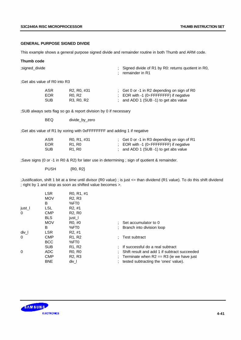
S3C2440A RISC MICROPROCESSOR THUMB INSTRUCTION SET
4-41
GENERAL PURPOSE SIGNED DIVIDE
This example shows a general purpose signed divide and remainder routine in both Thumb and ARM code.
Thumb code
;signed_divide ; Signed divide of R1 by R0: returns quotient in R0,; remainder in R1
;Get abs value of R0 into R3
ASR R2, R0, #31 ; Get 0 or -1 in R2 depending on sign of R0EOR R0, R2 ; EOR with -1 (0×FFFFFFFF) if negativeSUB R3, R0, R2 ; and ADD 1 (SUB -1) to get abs value
;SUB always sets flag so go & report division by 0 if necessary
BEQ divide_by_zero
;Get abs value of R1 by xoring with 0xFFFFFFFF and adding 1 if negative
ASR R0, R1, #31 ; Get 0 or -1 in R3 depending on sign of R1EOR R1, R0 ; EOR with -1 (0×FFFFFFFF) if negativeSUB R1, R0 ; and ADD 1 (SUB -1) to get abs value
;Save signs (0 or -1 in R0 & R2) for later use in determining ; sign of quotient & remainder.
PUSH R0, R2
;Justification, shift 1 bit at a time until divisor (R0 value) ; is just <= than dividend (R1 value). To do this shift dividend; right by 1 and stop as soon as shifted value becomes >.
LSR R0, R1, #1MOV R2, R3B %FT0
just_l LSL R2, #10 CMP R2, R0
BLS just_lMOV R0, #0 ; Set accumulator to 0B %FT0 ; Branch into division loop
div_l LSR R2, #10 CMP R1, R2 ; Test subtract
BCC %FT0SUB R1, R2 ; If successful do a real subtract
0 ADC R0, R0 ; Shift result and add 1 if subtract succeededCMP R2, R3 ; Terminate when R2 == R3 (ie we have justBNE div_l ; tested subtracting the 'ones' value).
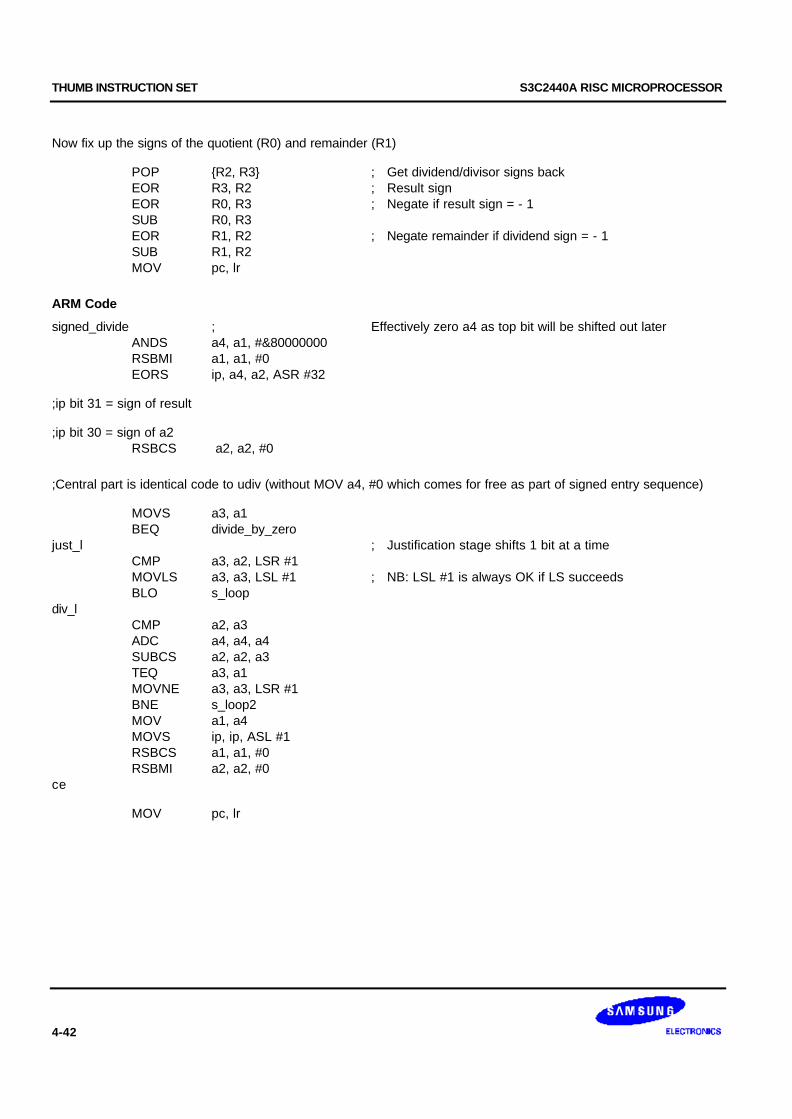
THUMB INSTRUCTION SET S3C2440A RISC MICROPROCESSOR
4-42
Now fix up the signs of the quotient (R0) and remainder (R1)
POP R2, R3 ; Get dividend/divisor signs backEOR R3, R2 ; Result signEOR R0, R3 ; Negate if result sign = - 1SUB R0, R3EOR R1, R2 ; Negate remainder if dividend sign = - 1SUB R1, R2MOV pc, lr
ARM Code
signed_divide ; Effectively zero a4 as top bit will be shifted out laterANDS a4, a1, #&80000000RSBMI a1, a1, #0EORS ip, a4, a2, ASR #32
;ip bit 31 = sign of result
;ip bit 30 = sign of a2RSBCS a2, a2, #0
;Central part is identical code to udiv (without MOV a4, #0 which comes for free as part of signed entry sequence)
MOVS a3, a1BEQ divide_by_zero
just_l ; Justification stage shifts 1 bit at a timeCMP a3, a2, LSR #1MOVLS a3, a3, LSL #1 ; NB: LSL #1 is always OK if LS succeedsBLO s_loop
div_lCMP a2, a3ADC a4, a4, a4SUBCS a2, a2, a3TEQ a3, a1MOVNE a3, a3, LSR #1BNE s_loop2MOV a1, a4MOVS ip, ip, ASL #1RSBCS a1, a1, #0RSBMI a2, a2, #0
ce
MOV pc, lr
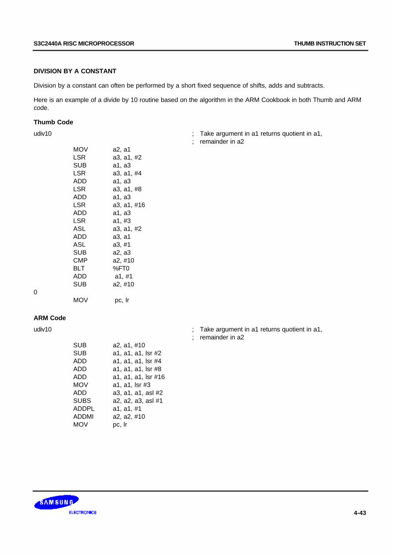
S3C2440A RISC MICROPROCESSOR THUMB INSTRUCTION SET
4-43
DIVISION BY A CONSTANT
Division by a constant can often be performed by a short fixed sequence of shifts, adds and subtracts.
Here is an example of a divide by 10 routine based on the algorithm in the ARM Cookbook in both Thumb and ARMcode.
Thumb Code
udiv10 ; Take argument in a1 returns quotient in a1,; remainder in a2
MOV a2, a1LSR a3, a1, #2SUB a1, a3LSR a3, a1, #4ADD a1, a3LSR a3, a1, #8ADD a1, a3LSR a3, a1, #16ADD a1, a3LSR a1, #3ASL a3, a1, #2ADD a3, a1ASL a3, #1SUB a2, a3CMP a2, #10BLT %FT0ADD a1, #1SUB a2, #10
0MOV pc, lr
ARM Code
udiv10 ; Take argument in a1 returns quotient in a1,; remainder in a2
SUB a2, a1, #10SUB a1, a1, a1, lsr #2ADD a1, a1, a1, lsr #4ADD a1, a1, a1, lsr #8ADD a1, a1, a1, lsr #16MOV a1, a1, lsr #3ADD a3, a1, a1, asl #2SUBS a2, a2, a3, asl #1ADDPL a1, a1, #1ADDMI a2, a2, #10MOV pc, lr

THUMB INSTRUCTION SET S3C2440A RISC MICROPROCESSOR
4-44
NOTES

S3C2440A RISC MICROPROCESSOR MEMORY CONTROLLER
5-1
5 MEMORY CONTROLLER
OVERVIEW
The S3C2440A memory controller provides memory control signals that are required for external memory access.
The S3C2440A has the following features:
— Little/Big endian (selectable by a software)
— Address space: 128Mbytes per bank (total 1GB/8 banks)
— Programmable access size (8/16/32-bit) for all banks except bank0 (16/32-bit)
— Total 8 memory banksSix memory banks for ROM, SRAM, etc.Remaining two memory banks for ROM, SRAM, SDRAM, etc .
— Seven fixed memory bank start address
— One flexible memory bank start address and programmable bank size
— Programmable access cycles for all memory banks
— External wait to extend the bus cycles
— Supporting self-refresh and power down mode in SDRAM
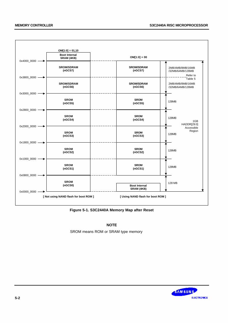
MEMORY CONTROLLER S3C2440A RISC MICROPROCESSOR
5-2
0x0000_0000
0x0800_0000
0x1000_0000
0x1800_0000
0x2000_0000
0x2800_0000
0x3000_0000
0x3800_0000
0x4000_0000
SROM/SDRAM(nGCS7)
SROM/SDRAM(nGCS6)
SROM(nGCS5)
SROM(nGCS4)
SROM(nGCS3)
SROM(nGCS2)
SROM(nGCS1)
Boot InternalSRAM (4KB)
128 MB
128MB
128MB
128MB
128MB
128MB
2MB/4MB/8MB/16MB/32MB/64MB/128MB
2MB/4MB/8MB/16MB/32MB/64MB/128MB
Refer toTable 5
1GBHADDR[29:0]
AccessibleRegion
SROM/SDRAM(nGCS7)
SROM/SDRAM(nGCS6)
SROM(nGCS5)
SROM(nGCS4)
SROM(nGCS3)
SROM(nGCS2)
SROM(nGCS1)
SROM(nGCS0)
OM[1:0] = 01,10
OM[1:0] = 00
[ Not using NAND flash for boot ROM ] [ Using NAND flash for boot ROM ]
Boot InternalSRAM (4KB)
Figure 5-1. S3C2440A Memory Map after Reset
NOTE
SROM means ROM or SRAM type memory
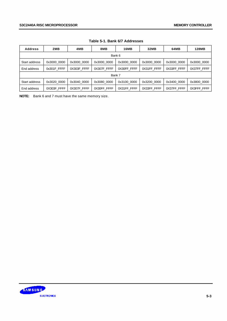
S3C2440A RISC MICROPROCESSOR MEMORY CONTROLLER
5-3
Table 5-1. Bank 6/7 Addresses
Address 2MB 4MB 8MB 16MB 32MB 64MB 128MB
Bank 6
Start address 0x3000_0000 0x3000_0000 0x3000_0000 0x3000_0000 0x3000_0000 0x3000_0000 0x3000_0000
End address 0x301F_FFFF 0X303F_FFFF 0X307F_FFFF 0X30FF_FFFF 0X31FF_FFFF 0X33FF_FFFF 0X37FF_FFFF
Bank 7
Start address 0x3020_0000 0x3040_0000 0x3080_0000 0x3100_0000 0x3200_0000 0x3400_0000 0x3800_0000
End address 0X303F_FFFF 0X307F_FFFF 0X30FF_FFFF 0X31FF_FFFF 0X33FF_FFFF 0X37FF_FFFF 0X3FFF_FFFF
NOTE: Bank 6 and 7 must have the same memory size.
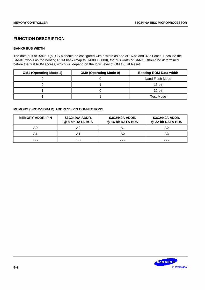
MEMORY CONTROLLER S3C2440A RISC MICROPROCESSOR
5-4
FUNCTION DESCRIPTION
BANK0 BUS WIDTH
The data bus of BANK0 (nGCS0) should be configured with a width as one of 16-bit and 32-bit ones. Because theBANK0 works as the booting ROM bank (map to 0x0000_0000), the bus width of BANK0 should be determinedbefore the first ROM access, which will depend on the logic level of OM[1:0] at Reset.
OM1 (Operating Mode 1) OM0 (Operating Mode 0) Booting ROM Data width
0 0 Nand Flash Mode
0 1 16-bit
1 0 32-bit
1 1 Test Mode
MEMORY (SROM/SDRAM) ADDRESS PIN CONNECTIONS
MEMORY ADDR. PIN S3C2440A ADDR.@ 8-bit DATA BUS
S3C2440A ADDR.@ 16-bit DATA BUS
S3C2440A ADDR.@ 32-bit DATA BUS
A0 A0 A1 A2
A1 A1 A2 A3
. . . . . . . . . . . .
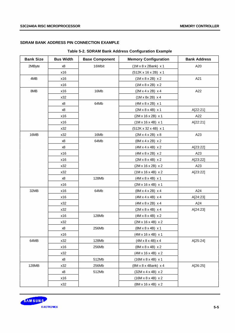
S3C2440A RISC MICROPROCESSOR MEMORY CONTROLLER
5-5
SDRAM BANK ADDRESS PIN CONNECTION EXAMPLE
Table 5-2. SDRAM Bank Address Configuration Example
Bank Size Bus Width Base Component Memory Configuration Bank Address
2MByte x8 16Mbit (1M x 8 x 2Bank) x 1 A20
x16 (512K x 16 x 2B) x 1
4MB x16 (1M x 8 x 2B) x 2 A21
x16 (1M x 8 x 2B) x 2
8MB x16 16Mb (2M x 4 x 2B) x 4 A22
x32 (1M x 8x 2B) x 4
x8 64Mb (4M x 8 x 2B) x 1
x8 (2M x 8 x 4B) x 1 A[22:21]
x16 (2M x 16 x 2B) x 1 A22
x16 (1M x 16 x 4B) x 1 A[22:21]
x32 (512K x 32 x 4B) x 1
16MB x32 16Mb (2M x 4 x 2B) x 8 A23
x8 64Mb (8M x 4 x 2B) x 2
x8 (4M x 4 x 4B) x 2 A[23:22]
x16 (4M x 8 x 2B) x 2 A23
x16 (2M x 8 x 4B) x 2 A[23:22]
x32 (2M x 16 x 2B) x 2 A23
x32 (1M x 16 x 4B) x 2 A[23:22]
x8 128Mb (4M x 8 x 4B) x 1
x16 (2M x 16 x 4B) x 1
32MB x16 64Mb (8M x 4 x 2B) x 4 A24
x16 (4M x 4 x 4B) x 4 A[24:23]
x32 (4M x 8 x 2B) x 4 A24
x32 (2M x 8 x 4B) x 4 A[24:23]
x16 128Mb (4M x 8 x 4B) x 2
x32 (2M x 16 x 4B) x 2
x8 256Mb (8M x 8 x 4B) x 1
x16 (4M x 16 x 4B) x 1
64MB x32 128Mb (4M x 8 x 4B) x 4 A[25:24]
x16 256Mb (8M x 8 x 4B) x 2
x32 (4M x 16 x 4B) x 2
x8 512Mb (16M x 8 x 4B) x 1
128MB x32 256Mb (8M x 8 x 4Bank) x 4 A[26:25]
x8 512Mb (32M x 4 x 4B) x 2
x16 (16M x 8 x 4B) x 2
x32 (8M x 16 x 4B) x 2

MEMORY CONTROLLER S3C2440A RISC MICROPROCESSOR
5-6
nWAIT PIN OPERATION
If the WAIT bit(WSn bit in BWSCON) corresponding to each memory bank is enabled, the nOE duration should beprolonged by the external nWAIT pin while the memory bank is active. nWAIT is checked from tacc-1. nOE will bede-asserted at the next clock after sampling nWAIT is high. The nWE signal have the same relation with nOE.
Tacs
Tcos
Tacc=4
HCLK
ADDR
nGCS
nOE
nWAIT
DATA(R)
Delayed
Sampling nWAIT
Figure 5-2. S3C2440A External nWAIT Timing Diagram (Tacc=4)
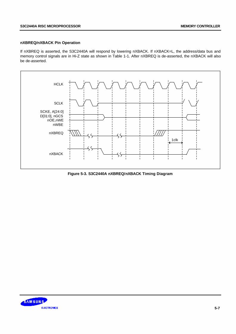
S3C2440A RISC MICROPROCESSOR MEMORY CONTROLLER
5-7
nXBREQ/nXBACK Pin Operation
If nXBREQ is asserted, the S3C2440A will respond by lowering nXBACK. If nXBACK=L, the address/data bus andmemory control signals are in Hi-Z state as shown in Table 1-1. After nXBREQ is de-asserted, the nXBACK will alsobe de-asserted.
HCLK
SCKE, A[24:0]D[31:0], nGCS
nOE,nWEnWBE
nXBREQ
nXBACK
SCLK
1clk
Figure 5-3. S3C2440A nXBREQ/nXBACK Timing Diagram
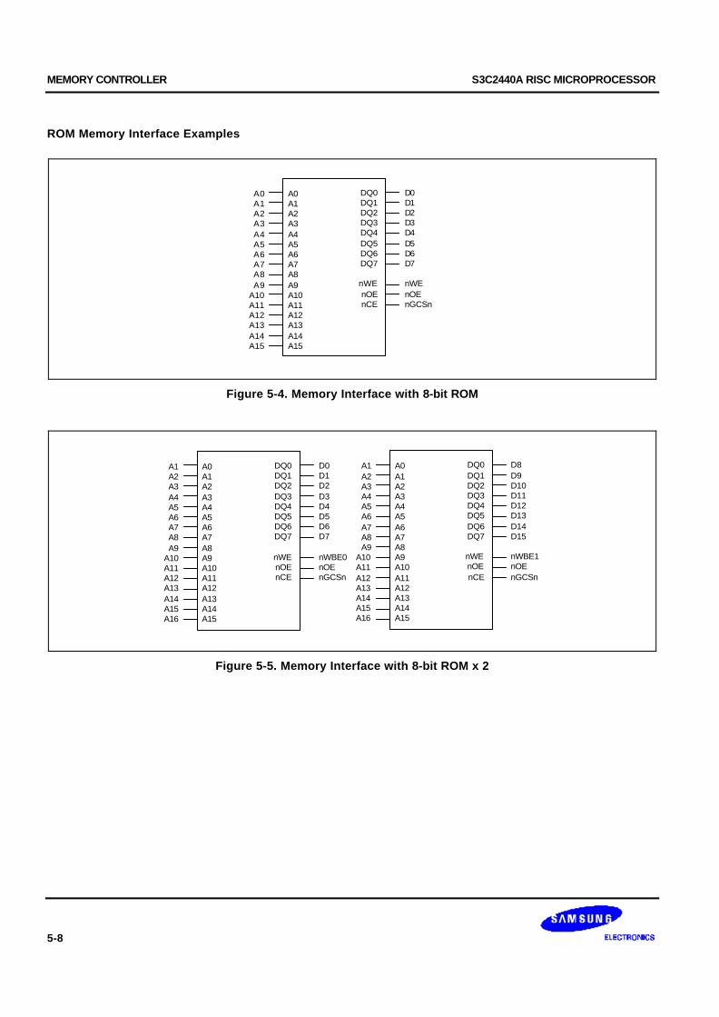
MEMORY CONTROLLER S3C2440A RISC MICROPROCESSOR
5-8
ROM Memory Interface Examples
A0A1A2A3A4A5A6A7A8A9
A10A11A12A13A14A15
D0D1D2D3D4D5D6D7
nWEnOEnGCSn
A0A1A2A3A4A5A6A7A8A9A10A11A12A13A14A15
DQ0DQ1DQ2DQ3DQ4DQ5DQ6DQ7
nWEnOEnCE
Figure 5-4. Memory Interface with 8-bit ROM
A1A2A3A4A5A6A7A8A9
A10A11A12A13A14A15A16
D0D1D2D3D4D5D6D7
nWBE0nOEnGCSn
A0A1A2A3A4A5A6A7A8A9A10A11A12A13A14A15
DQ0DQ1DQ2DQ3DQ4DQ5DQ6DQ7
nWEnOEnCE
A1A2A3A4A5A6A7A8A9
A10A11A12A13A14A15A16
D8D9D10D11D12D13D14D15
nWBE1nOEnGCSn
A0A1A2A3A4A5A6A7A8A9A10A11A12A13A14A15
DQ0DQ1DQ2DQ3DQ4DQ5DQ6DQ7
nWEnOEnCE
Figure 5-5. Memory Interface with 8-bit ROM x 2
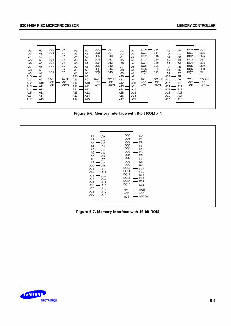
S3C2440A RISC MICROPROCESSOR MEMORY CONTROLLER
5-9
A2A3A4A5A6A7A8A9
A10A11A12A13A14A15A16A17
A0A1A2A3A4A5A6A7A8A9A10A11A12A13A14A15
DQ0DQ1DQ2DQ3DQ4DQ5DQ6DQ7
nWEnOEnCE
D0D1D2D3D4D5D6D7
nWBE0nOEnGCSn
A2A3A4A5A6A7A8A9
A10A11A12A13A14A15A16A17
A0A1A2A3A4A5A6A7A8A9A10A11A12A13A14A15
DQ0DQ1DQ2DQ3DQ4DQ5DQ6DQ7
nWEnOEnCE
D8D9D10D11D12D13D14D15
nWBE1nOEnGCSn
A2A3A4A5A6A7A8A9
A10A11A12A13A14A15A16A17
A0A1A2A3A4A5A6A7A8A9A10A11A12A13A14A15
DQ0DQ1DQ2DQ3DQ4DQ5DQ6DQ7
nWEnOEnCE
D16D17D18D19D20D21D22D23
nWBE2nOEnGCSn
A2A3A4A5A6A7A8A9
A10A11A12A13A14A15A16A17
A0A1A2A3A4A5A6A7A8A9A10A11A12A13A14A15
DQ0DQ1DQ2DQ3DQ4DQ5DQ6DQ7
nWEnOEnCE
D24D25D26D27D28D29D30D31
nWBE3nOEnGCSn
Figure 5-6. Memory Interface with 8-bit ROM x 4
A1A2A3A4A5A6A7A8A9
A10A11A12A13A14A15A16A17A18A19
D0D1D2D3D4D5D6D7D8D9D10D11D12D13D14D15
A0A1A2A3A4A5A6A7A8A9A10A11A12A13A14A15A16A17A18
DQ0DQ1DQ2DQ3DQ4DQ5DQ6DQ7DQ8DQ9
DQ10DQ11DQ12DQ13DQ14DQ15
nWEnOEnCE
nWEnOEnGCSn
Figure 5-7. Memory Interface with 16-bit ROM
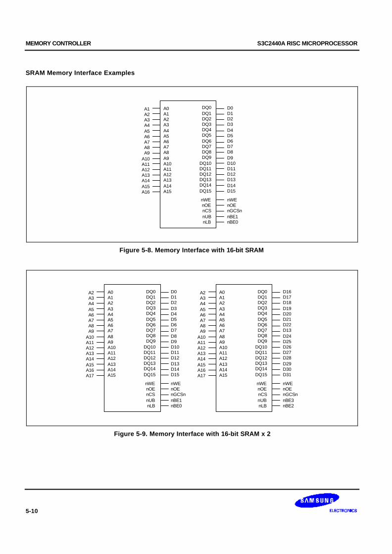
MEMORY CONTROLLER S3C2440A RISC MICROPROCESSOR
5-10
SRAM Memory Interface Examples
A1A2A3A4A5A6A7A8A9
A10A11A12A13A14A15A16
D0D1D2D3D4D5D6D7D8D9D10D11D12D13D14D15
A0A1A2A3A4A5A6A7A8A9A10A11A12A13A14A15
DQ0DQ1DQ2DQ3DQ4DQ5DQ6DQ7DQ8DQ9
DQ10DQ11DQ12DQ13DQ14DQ15
nWEnOEnCS
nWEnOEnGCSn
nUBnLB
nBE1nBE0
Figure 5-8. Memory Interface with 16-bit SRAM
A2A3A4A5A6A7A8A9
A10A11A12A13A14A15A16A17
D0D1D2D3D4D5D6D7D8D9D10D11D12D13D14D15
A0A1A2A3A4A5A6A7A8A9A10A11A12A13A14A15
DQ0DQ1DQ2DQ3DQ4DQ5DQ6DQ7DQ8DQ9
DQ10DQ11DQ12DQ13DQ14DQ15
nWEnOEnCS
nWEnOEnGCSn
nUBnLB
nBE1nBE0
A2A3A4A5A6A7A8A9
A10A11A12A13A14A15A16A17
D16D17D18D19D20D21D22D13D24D25D26D27D28D29D30D31
A0A1A2A3A4A5A6A7A8A9A10A11A12A13A14A15
DQ0DQ1DQ2DQ3DQ4DQ5DQ6DQ7DQ8DQ9
DQ10DQ11DQ12DQ13DQ14DQ15
nWEnOEnCS
nWEnOEnGCSn
nUBnLB
nBE3nBE2
Figure 5-9. Memory Interface with 16-bit SRAM x 2

S3C2440A RISC MICROPROCESSOR MEMORY CONTROLLER
5-11
SDRAM Memory Interface Examples
A1A2A3A4A5A6A7A8A9
A10A11A12
D0D1D2D3D4D5D6D7D8D9D10D11D12D13D14D15
A0A1A2A3A4A5A6A7A8A9A10A11
DQ0DQ1DQ2DQ3DQ4DQ5DQ6DQ7DQ8DQ9
DQ10DQ11DQ12DQ13DQ14DQ15
BA0BA1LDQMUDQM
A21A22
DQM0DQM1
SCKESCLK
SCKESCLK
nSCS0nSRASnSCASnWE
nSCSnSRASnSCAS
nWE
Figure 5-10. Memory Interface with 16-bit SDRAM (4Mx16, 4banks)
A2A3A4A5A6A7A8A9
A10A11A12A13A14
D0D1D2D3D4D5D6D7D8D9D10D11D12D13D14D15
A0A1A2A3A4A5A6A7A8A9A10A11A12
DQ0DQ1DQ2DQ3DQ4DQ5DQ6DQ7DQ8DQ9
DQ10DQ11DQ12DQ13DQ14DQ15
BA0BA1LDQMUDQM
A24A25
DQM0DQM1
SCKESCLK
SCKESCLK
nSCS0nSRASnSCASnWE
nSCSnSRASnSCAS
nWE
A2A3A4A5A6A7A8A9
A10A11A12A13A14
A0A1A2A3A4A5A6A7A8A9A10A11A12
DQ0DQ1DQ2DQ3DQ4DQ5DQ6DQ7DQ8DQ9
DQ10DQ11DQ12DQ13DQ14DQ15
BA0BA1LDQMUDQM
A24A25
DQM2DQM3
SCKESCLK
SCKESCLK
nSCS0nSRASnSCASnWE
nSCSnSRASnSCAS
nWE
D16D17D18D19D20D21D22D23D24D25D26D27D28D29D30D31
Figure 5-11. Memory Interface with 16-bit SDRAM (4Mx16x4Bank * 2ea)
NOTE
Refer to Table 5-2 for the Bank Address configurations of SDRAM.
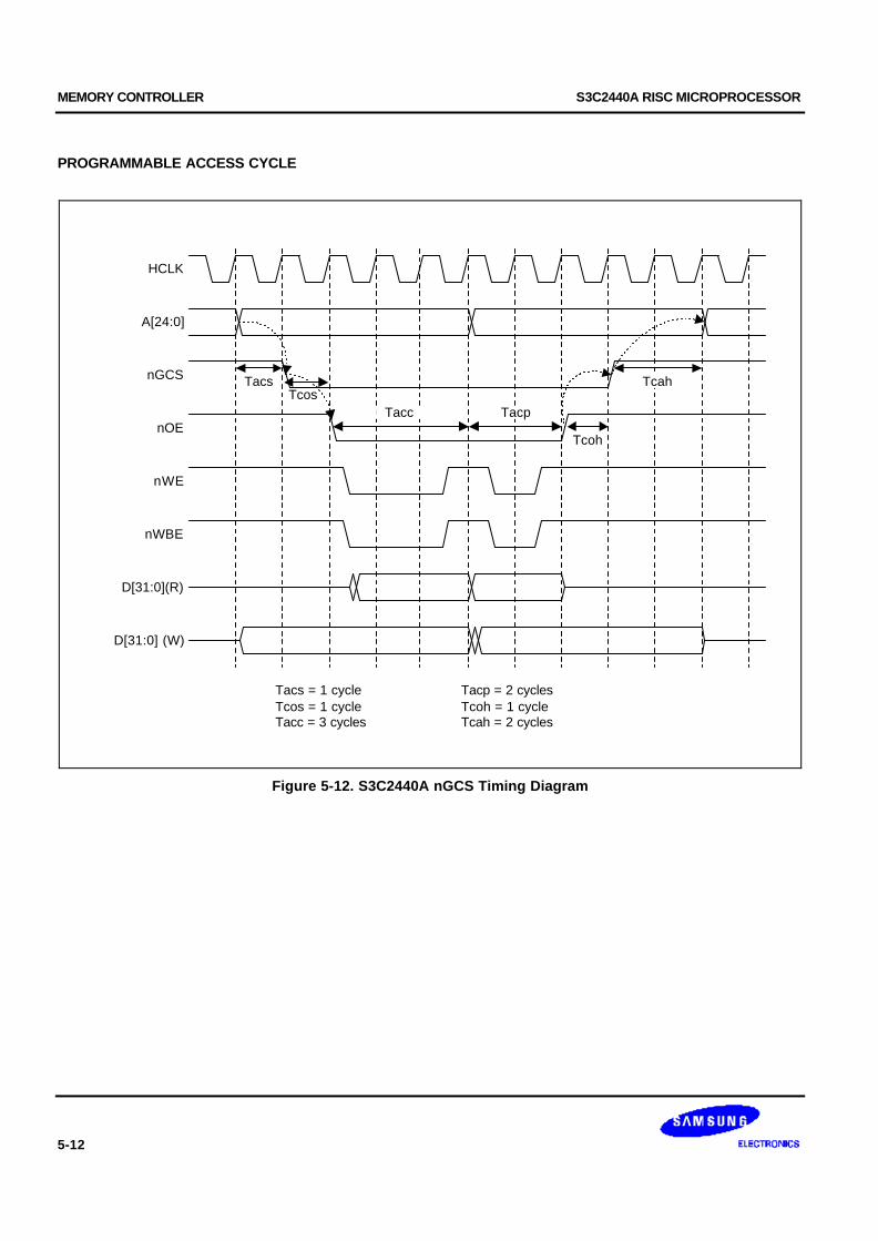
MEMORY CONTROLLER S3C2440A RISC MICROPROCESSOR
5-12
PROGRAMMABLE ACCESS CYCLE
Tcoh
TcosTacs
HCLK
A[24:0]
nGCS
nOE
nWE
nWBE
D[31:0](R)
D[31:0] (W)
Tacc Tacp
Tcah
Tacs = 1 cycleTcos = 1 cycleTacc = 3 cycles
Tacp = 2 cyclesTcoh = 1 cycleTcah = 2 cycles
Figure 5-12. S3C2440A nGCS Timing Diagram
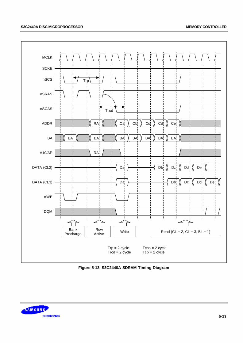
S3C2440A RISC MICROPROCESSOR MEMORY CONTROLLER
5-13
MCLK
SCKE
nSCS
nSCAS
ADDR
A10/AP
RA
nSRAS
BA
DATA (CL2)
DATA (CL3)
nWE
DQM
Trp
Trcd
RA
Ca
Da
Da
BABA
Cb Cc Cd Ce
Db Dc Dd De
Db Dc Dd De
BA BA BA BA BA
BankPrecharge
RowActive Write Read (CL = 2, CL = 3, BL = 1)
Trp = 2 cycle Tcas = 2 cycleTrcd = 2 cycle Tcp = 2 cycle
Figure 5-13. S3C2440A SDRAM Timing Diagram
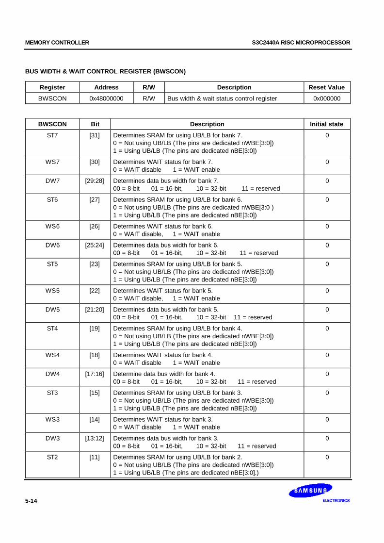
MEMORY CONTROLLER S3C2440A RISC MICROPROCESSOR
5-14
BUS WIDTH & WAIT CONTROL REGISTER (BWSCON)
Register Address R/W Description Reset Value
BWSCON 0x48000000 R/W Bus width & wait status control register 0x000000
BWSCON Bit Description Initial state
ST7 [31] Determines SRAM for using UB/LB for bank 7.0 = Not using UB/LB (The pins are dedicated nWBE[3:0])1 = Using UB/LB (The pins are dedicated nBE[3:0])
0
WS7 [30] Determines WAIT status for bank 7.0 = WAIT disable 1 = WAIT enable
0
DW7 [29:28] Determines data bus width for bank 7.00 = 8-bit 01 = 16-bit, 10 = 32-bit 11 = reserved
0
ST6 [27] Determines SRAM for using UB/LB for bank 6.0 = Not using UB/LB (The pins are dedicated nWBE[3:0 )1 = Using UB/LB (The pins are dedicated nBE[3:0])
0
WS6 [26] Determines WAIT status for bank 6.0 = WAIT disable, 1 = WAIT enable
0
DW6 [25:24] Determines data bus width for bank 6.00 = 8-bit 01 = 16-bit, 10 = 32-bit 11 = reserved
0
ST5 [23] Determines SRAM for using UB/LB for bank 5.0 = Not using UB/LB (The pins are dedicated nWBE[3:0])1 = Using UB/LB (The pins are dedicated nBE[3:0])
0
WS5 [22] Determines WAIT status for bank 5.0 = WAIT disable, 1 = WAIT enable
0
DW5 [21:20] Determines data bus width for bank 5.00 = 8-bit 01 = 16-bit, 10 = 32-bit 11 = reserved
0
ST4 [19] Determines SRAM for using UB/LB for bank 4.0 = Not using UB/LB (The pins are dedicated nWBE[3:0])1 = Using UB/LB (The pins are dedicated nBE[3:0])
0
WS4 [18] Determines WAIT status for bank 4.0 = WAIT disable 1 = WAIT enable
0
DW4 [17:16] Determine data bus width for bank 4.00 = 8-bit 01 = 16-bit, 10 = 32-bit 11 = reserved
0
ST3 [15] Determines SRAM for using UB/LB for bank 3.0 = Not using UB/LB (The pins are dedicated nWBE[3:0])1 = Using UB/LB (The pins are dedicated nBE[3:0])
0
WS3 [14] Determines WAIT status for bank 3.0 = WAIT disable 1 = WAIT enable
0
DW3 [13:12] Determines data bus width for bank 3.00 = 8-bit 01 = 16-bit, 10 = 32-bit 11 = reserved
0
ST2 [11] Determines SRAM for using UB/LB for bank 2.0 = Not using UB/LB (The pins are dedicated nWBE[3:0])1 = Using UB/LB (The pins are dedicated nBE[3:0].)
0
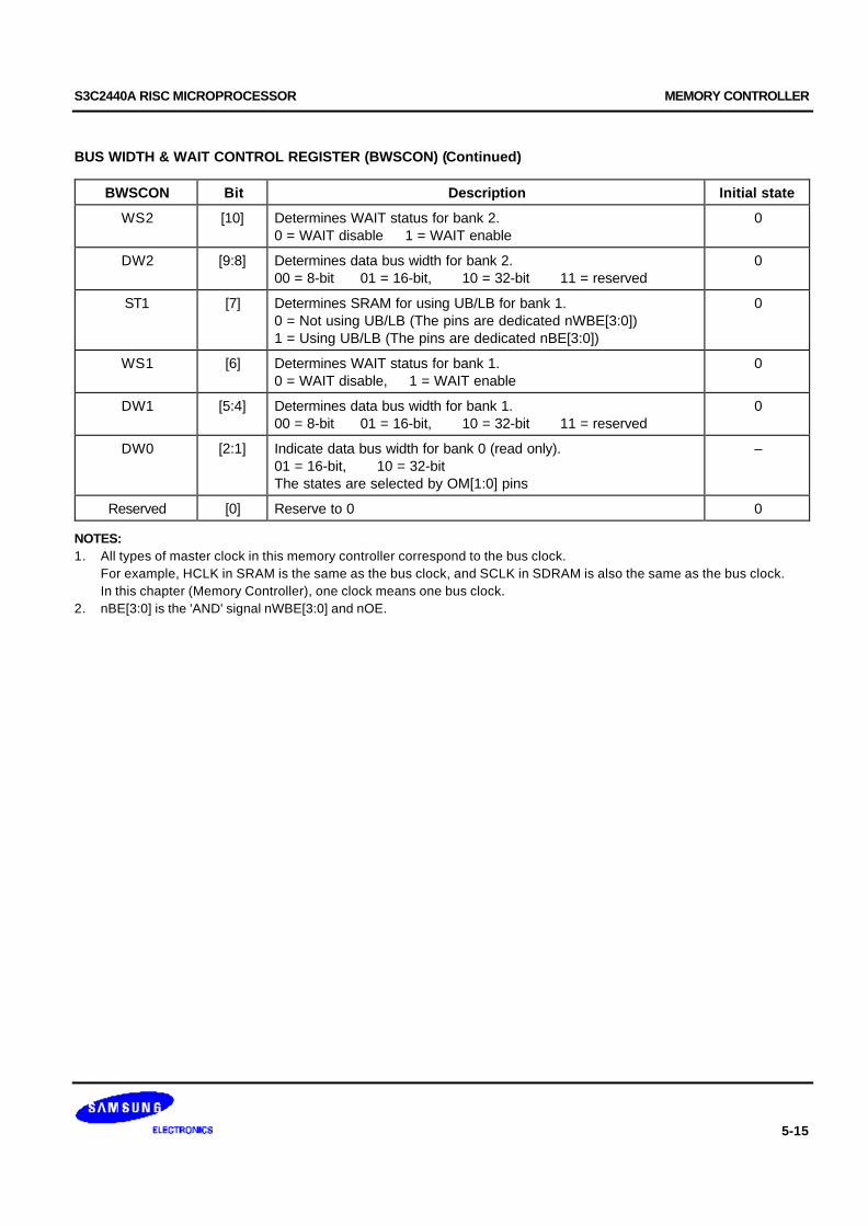
S3C2440A RISC MICROPROCESSOR MEMORY CONTROLLER
5-15
BUS WIDTH & WAIT CONTROL REGISTER (BWSCON) (Continued)
BWSCON Bit Description Initial state
WS2 [10] Determines WAIT status for bank 2.0 = WAIT disable 1 = WAIT enable
0
DW2 [9:8] Determines data bus width for bank 2.00 = 8-bit 01 = 16-bit, 10 = 32-bit 11 = reserved
0
ST1 [7] Determines SRAM for using UB/LB for bank 1.0 = Not using UB/LB (The pins are dedicated nWBE[3:0])1 = Using UB/LB (The pins are dedicated nBE[3:0])
0
WS1 [6] Determines WAIT status for bank 1.0 = WAIT disable, 1 = WAIT enable
0
DW1 [5:4] Determines data bus width for bank 1.00 = 8-bit 01 = 16-bit, 10 = 32-bit 11 = reserved
0
DW0 [2:1] Indicate data bus width for bank 0 (read only).01 = 16-bit, 10 = 32-bitThe states are selected by OM[1:0] pins
–
Reserved [0] Reserve to 0 0
NOTES:1. All types of master clock in this memory controller correspond to the bus clock.
For example, HCLK in SRAM is the same as the bus clock, and SCLK in SDRAM is also the same as the bus clock.In this chapter (Memory Controller), one clock means one bus clock.
2. nBE[3:0] is the 'AND' signal nWBE[3:0] and nOE.
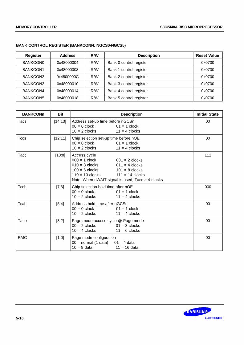
MEMORY CONTROLLER S3C2440A RISC MICROPROCESSOR
5-16
BANK CONTROL REGISTER (BANKCONN: NGCS0-NGCS5)
Register Address R/W Description Reset Value
BANKCON0 0x48000004 R/W Bank 0 control register 0x0700
BANKCON1 0x48000008 R/W Bank 1 control register 0x0700
BANKCON2 0x4800000C R/W Bank 2 control register 0x0700
BANKCON3 0x48000010 R/W Bank 3 control register 0x0700
BANKCON4 0x48000014 R/W Bank 4 control register 0x0700
BANKCON5 0x48000018 R/W Bank 5 control register 0x0700
BANKCONn Bit Description Initial State
Tacs [14:13] Address set-up time before nGCSn00 = 0 clock 01 = 1 clock10 = 2 clocks 11 = 4 clocks
00
Tcos [12:11] Chip selection set-up time before nOE00 = 0 clock 01 = 1 clock10 = 2 clocks 11 = 4 clocks
00
Tacc [10:8] Access cycle000 = 1 clock 001 = 2 clocks010 = 3 clocks 011 = 4 clocks100 = 6 clocks 101 = 8 clocks110 = 10 clocks 111 = 14 clocksNote: When nWAIT signal is used, Tacc ≥ 4 clocks.
111
Tcoh [7:6] Chip selection hold time after nOE00 = 0 clock 01 = 1 clock10 = 2 clocks 11 = 4 clocks
000
Tcah [5:4] Address hold time after nGCSn00 = 0 clock 01 = 1 clock10 = 2 clocks 11 = 4 clocks
00
Tacp [3:2] Page mode access cycle @ Page mode00 = 2 clocks 01 = 3 clocks10 = 4 clocks 11 = 6 clocks
00
PMC [1:0] Page mode configuration00 = normal (1 data) 01 = 4 data10 = 8 data 11 = 16 data
00
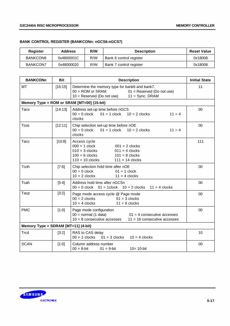
S3C2440A RISC MICROPROCESSOR MEMORY CONTROLLER
5-17
BANK CONTROL REGISTER (BANKCONn: nGCS6-nGCS7)
Register Address R/W Description Reset Value
BANKCON6 0x4800001C R/W Bank 6 control register 0x18008
BANKCON7 0x48000020 R/W Bank 7 control register 0x18008
BANKCONn Bit Description Initial State
MT [16:15] Determine the memory type for bank6 and bank7.00 = ROM or SRAM 01 = Reserved (Do not use)10 = Reserved (Do not use) 11 = Sync. DRAM
11
Memory Type = ROM or SRAM [MT=00] (15-bit)
Tacs [14:13] Address set-up time before nGCS00 = 0 clock 01 = 1 clock 10 = 2 clocks 11 = 4clocks
00
Tcos [12:11] Chip selection set-up time before nOE00 = 0 clock 01 = 1 clock 10 = 2 clocks 11 = 4clocks
00
Tacc [10:8] Access cycle000 = 1 clock 001 = 2 clocks010 = 3 clocks 011 = 4 clocks100 = 6 clocks 101 = 8 clocks110 = 10 clocks 111 = 14 clocks
111
Tcoh [7:6] Chip selection hold time after nOE00 = 0 clock 01 = 1 clock10 = 2 clocks 11 = 4 clocks
00
Tcah [5:4] Address hold time after nGCSn00 = 0 clock 01 = 1clock 10 = 2 clocks 11 = 4 clocks
00
Tacp [3:2] Page mode access cycle @ Page mode00 = 2 clocks 01 = 3 clocks10 = 4 clocks 11 = 6 clocks
00
PMC [1:0] Page mode configuration00 = normal (1 data) 01 = 4 consecutive accesses10 = 8 consecutive accesses 11 = 16 consecutive accesses
00
Memory Type = SDRAM [MT=11] (4-bit)
Trcd [3:2] RAS to CAS delay00 = 2 clocks 01 = 3 clocks 10 = 4 clocks
10
SCAN [1:0] Column address number00 = 8-bit 01 = 9-bit 10= 10-bit
00
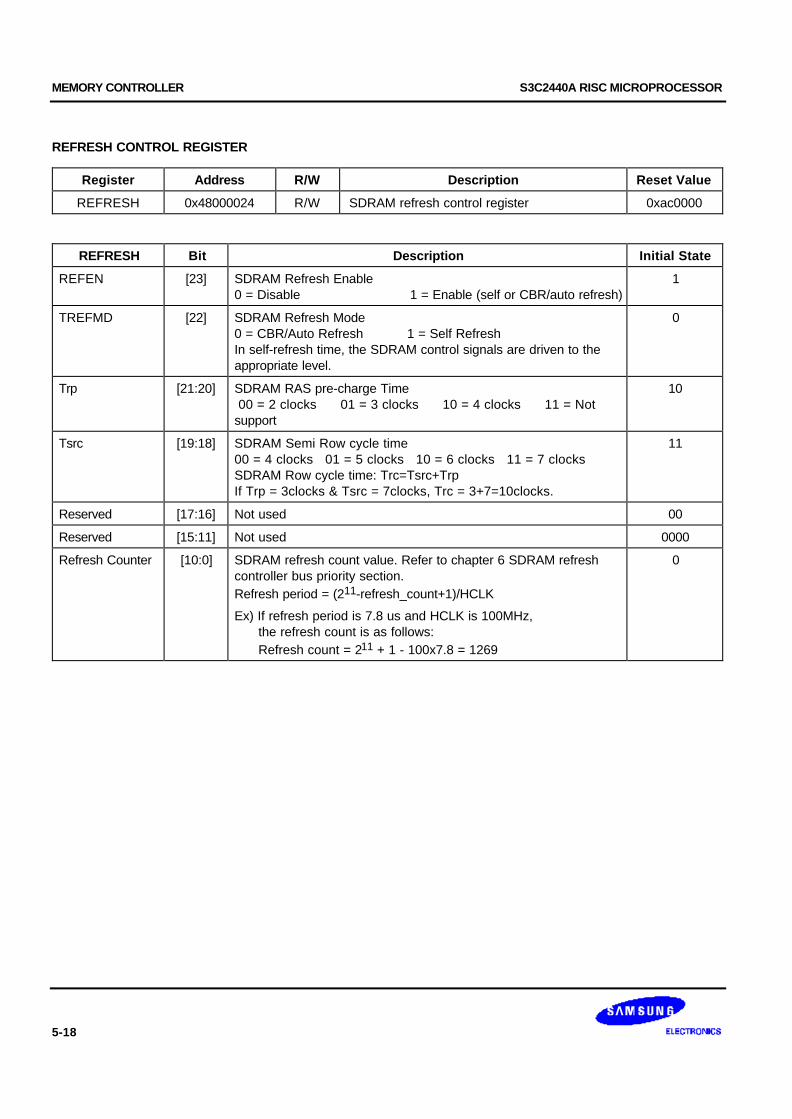
MEMORY CONTROLLER S3C2440A RISC MICROPROCESSOR
5-18
REFRESH CONTROL REGISTER
Register Address R/W Description Reset Value
REFRESH 0x48000024 R/W SDRAM refresh control register 0xac0000
REFRESH Bit Description Initial State
REFEN [23] SDRAM Refresh Enable0 = Disable 1 = Enable (self or CBR/auto refresh)
1
TREFMD [22] SDRAM Refresh Mode0 = CBR/Auto Refresh 1 = Self RefreshIn self-refresh time, the SDRAM control signals are driven to theappropriate level.
0
Trp [21:20] SDRAM RAS pre-charge Time 00 = 2 clocks 01 = 3 clocks 10 = 4 clocks 11 = Notsupport
10
Tsrc [19:18] SDRAM Semi Row cycle time00 = 4 clocks 01 = 5 clocks 10 = 6 clocks 11 = 7 clocksSDRAM Row cycle time: Trc=Tsrc+TrpIf Trp = 3clocks & Tsrc = 7clocks, Trc = 3+7=10clocks.
11
Reserved [17:16] Not used 00
Reserved [15:11] Not used 0000
Refresh Counter [10:0] SDRAM refresh count value. Refer to chapter 6 SDRAM refreshcontroller bus priority section.Refresh period = (211-refresh_count+1)/HCLK
Ex) If refresh period is 7.8 us and HCLK is 100MHz, the refresh count is as follows: Refresh count = 211 + 1 - 100x7.8 = 1269
0
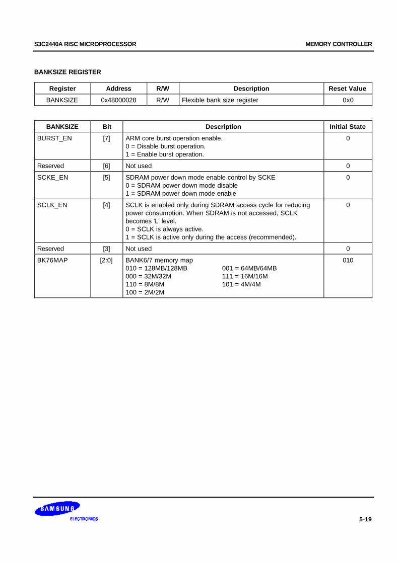
S3C2440A RISC MICROPROCESSOR MEMORY CONTROLLER
5-19
BANKSIZE REGISTER
Register Address R/W Description Reset Value
BANKSIZE 0x48000028 R/W Flexible bank size register 0x0
BANKSIZE Bit Description Initial State
BURST_EN [7] ARM core burst operation enable.0 = Disable burst operation.1 = Enable burst operation.
0
Reserved [6] Not used 0
SCKE_EN [5] SDRAM power down mode enable control by SCKE0 = SDRAM power down mode disable1 = SDRAM power down mode enable
0
SCLK_EN [4] SCLK is enabled only during SDRAM access cycle for reducingpower consumption. When SDRAM is not accessed, SCLKbecomes 'L' level.0 = SCLK is always active.1 = SCLK is active only during the access (recommended).
0
Reserved [3] Not used 0
BK76MAP [2:0] BANK6/7 memory map010 = 128MB/128MB 001 = 64MB/64MB000 = 32M/32M 111 = 16M/16M110 = 8M/8M 101 = 4M/4M100 = 2M/2M
010
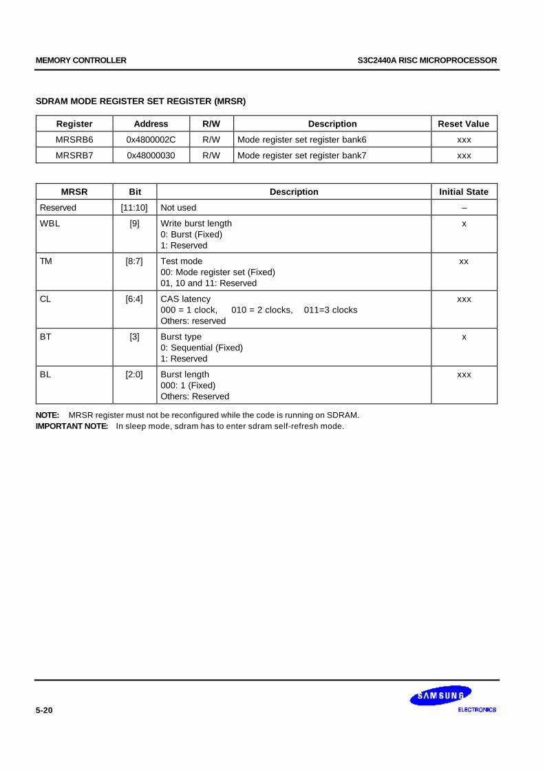
MEMORY CONTROLLER S3C2440A RISC MICROPROCESSOR
5-20
SDRAM MODE REGISTER SET REGISTER (MRSR)
Register Address R/W Description Reset Value
MRSRB6 0x4800002C R/W Mode register set register bank6 xxx
MRSRB7 0x48000030 R/W Mode register set register bank7 xxx
MRSR Bit Description Initial State
Reserved [11:10] Not used –
WBL [9] Write burst length0: Burst (Fixed)1: Reserved
x
TM [8:7] Test mode00: Mode register set (Fixed)01, 10 and 11: Reserved
xx
CL [6:4] CAS latency000 = 1 clock, 010 = 2 clocks, 011=3 clocksOthers: reserved
xxx
BT [3] Burst type0: Sequential (Fixed)1: Reserved
x
BL [2:0] Burst length000: 1 (Fixed)Others: Reserved
xxx
NOTE: MRSR register must not be reconfigured while the code is running on SDRAM.IMPORTANT NOTE: In sleep mode, sdram has to enter sdram self-refresh mode.
S3C2440A RISC MICROPROCESSOR NAND FLASH CONTROLLER
6-1
6 NAND FLASH CONTORLLER
OVERVIEW
In recent times, NOR flash memory gets high in price while an SDRAM and a NAND flash memory is comparativelyeconomical , motivating some users to execute the boot code on a NAND flash and execute the main code on anSDRAM.
S3C2440A boot code can be executed on an external NAND flash memory. In order to support NAND flash bootloader, the S3C2440A is equipped with an internal SRAM buffer called ‘Steppingstone’. When booting, the first 4KBytes of the NAND flash memory will be loaded into Steppingstone and the boot code loaded into Steppingstonewill be executed.
Generally, the boot code will copy NAND flash content to SDRAM. Using hardware ECC, the NAND flash datavalidity will be checked. Upon the completion of the copy, the main program will be executed on the SDRAM.
FEATURES
1. Auto boot: The boot code is transferred into 4-kbytes Steppingstone during reset. After the transfer, the bootcode will be executed on the Steppingstone.
2. NAND Flash memory I/F: Support 256Words, 512Bytes, 1KWords and 2KBytes Page.
3. Software mode: User can directly access NAND flash memory, for example this feature can be used inread/erase/program NAND flash memory.
4. Interface: 8 / 16-bit NAND flash memory interface bus.
5. Hardware ECC generation, detection and indication (Software correction).
6. SFR I/F: Support Little Endian Mode, Byte/half word/word access to Data and ECC Data register, and Wordaccess to other registers
7. SteppingStone I/F: Support Little/Big Endian, Byte/half word/word access.
8. The Steppingstone 4-KB internal SRAM buffer can be used for another purpose after NAND flash booting.
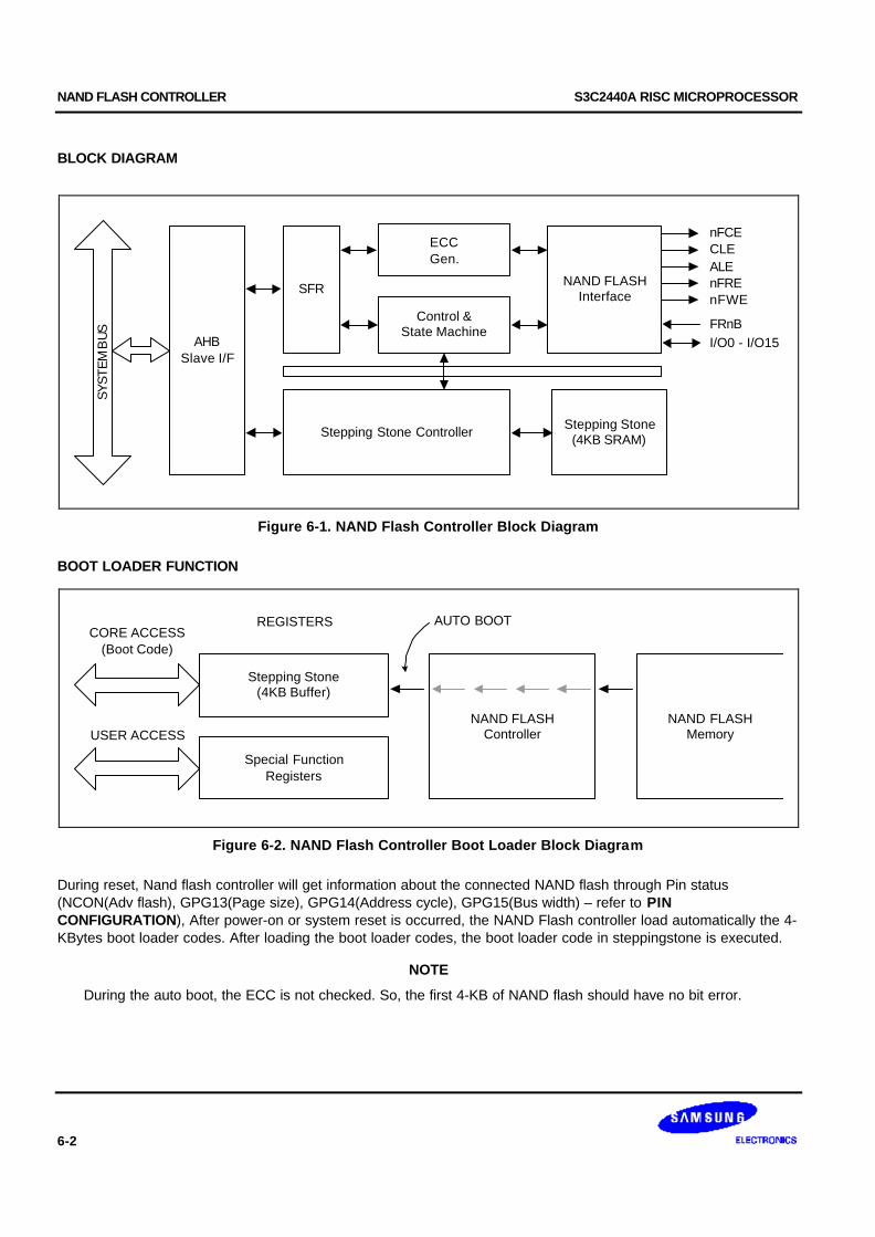
NAND FLASH CONTROLLER S3C2440A RISC MICROPROCESSOR
6-2
BLOCK DIAGRAM
SFR
ECCGen.
Stepping Stone(4KB SRAM)Stepping Stone Controller
SYST
EMB
US
NAND FLASHInterface
CLEALE
nFCE
nFREnFWE
FRnBI/O0 - I/O15AHB
Slave I/F
Control &State Machine
Figure 6-1. NAND Flash Controller Block Diagram
BOOT LOADER FUNCTION
Stepping Stone(4KB Buffer)
NAND FLASHController
NAND FLASHMemory
Special FunctionRegisters
REGISTERS AUTO BOOTCORE ACCESS
(Boot Code)
USER ACCESS
Figure 6-2. NAND Flash Controller Boot Loader Block Diagram
During reset, Nand flash controller will get information about the connected NAND flash through Pin status(NCON(Adv flash), GPG13(Page size), GPG14(Address cycle), GPG15(Bus width) – refer to PINCONFIGURATION), After power-on or system reset is occurred, the NAND Flash controller load automatically the 4-KBytes boot loader codes. After loading the boot loader codes, the boot loader code in steppingstone is executed.
NOTE
During the auto boot, the ECC is not checked. So, the first 4-KB of NAND flash should have no bit error.

S3C2440A RISC MICROPROCESSOR NAND FLASH CONTROLLER
6-3
PIN CONFIGURATION
OM[1:0] = 00: Enable NAND flash memory boot
NCON: NAND flash memory selection(Normal / Advance)0: Normal NAND flash(256Words/512Bytes page size, 3/4 address cycle)1: Advance NAND flash(1KWords/2KBytes page size, 4/5 address cycle)
GPG13: NAND flash memory page capacitance selection0: Page=256Words(NCON = 0) or Page=1KWords(NCON = 1)1: Page=512Bytes(NCON = 0) or Page=2KBytes(NCON = 1)
GPG14: NAND flash memory address cycle selection0: 3 address cycle(NCON = 0) or 4 address cycle(NCON = 1)1: 4 address cycle(NCON = 0) or 5 address cycle(NCON = 1)
GPG15: NAND flash memory bus width selection0: 8-bit bus width1: 16-bit bus width
NOTE
The configuration pin – NCON, GPG[15:13] – will be fetched during reset.In normal status, these pins must be set as input so that the pin status is not to be changed, when entersSleep mode by software or unexpected cause.
NAND FLASH MEMORY CONFIGURATION TABLE
NCON0 GPG13 GPG14 GPG15
0: Normal NAND 0: 256Words 0: 3-Addr 0: 8-bit bus width
1: 512Bytes 1: 4-Addr
1: Advance NAND 0: 1Kwords 0: 4-Addr 1: 16-bit bus width
1: 2Kbytes 1: 5-Addr
NOTE: With above 4-bit, Possible total combinations are 16, but not all the value can be used.
Example) Nand flash configuration setting.
Parts Page size/Total size NCON0 GPG13 GPG14] GPG15
K9S1208V0M-xxxx 512Byte / 512Mbit 0 1 1 0
K9K2G16U0M-xxxx 1KW / 2Gbit 1 0 1 1
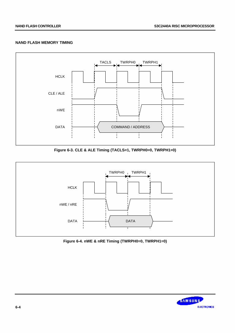
NAND FLASH CONTROLLER S3C2440A RISC MICROPROCESSOR
6-4
NAND FLASH MEMORY TIMING
HCLK
CLE / ALE
nWE
TACLS TWRPH0 TWRPH1
DATA COMMAND / ADDRESS
Figure 6-3. CLE & ALE Timing (TACLS=1, TWRPH0=0, TWRPH1=0)
HCLK
nWE / nRE
DATA DATA
TWRPH0 TWRPH1
Figure 6-4. nWE & nRE Timing (TWRPH0=0, TWRPH1=0)
S3C2440A RISC MICROPROCESSOR NAND FLASH CONTROLLER
6-5
SOFTWARE MODE
S3C2440A supports only software mode access. Using this mode, you can completely access the NAND flashmemory. The NAND Flash Controller supports direct access interface with the NAND flash memory.
1. Writing to the command register = the NAND Flash Memory command cycle
2. Writing to the address register = the NAND Flash Memory address cycle
3. Writing to the data register = write data to the NAND Flash Memory (write cycle)
4. Reading from the data register = read data from the NAND Flash Memory (read cycle)
5. Reading main ECC registers and Spare ECC registers = read data from the NAND Flash Memory
NOTE
In the software mode, you have to check the RnB status input pin by using polling or interrupt.
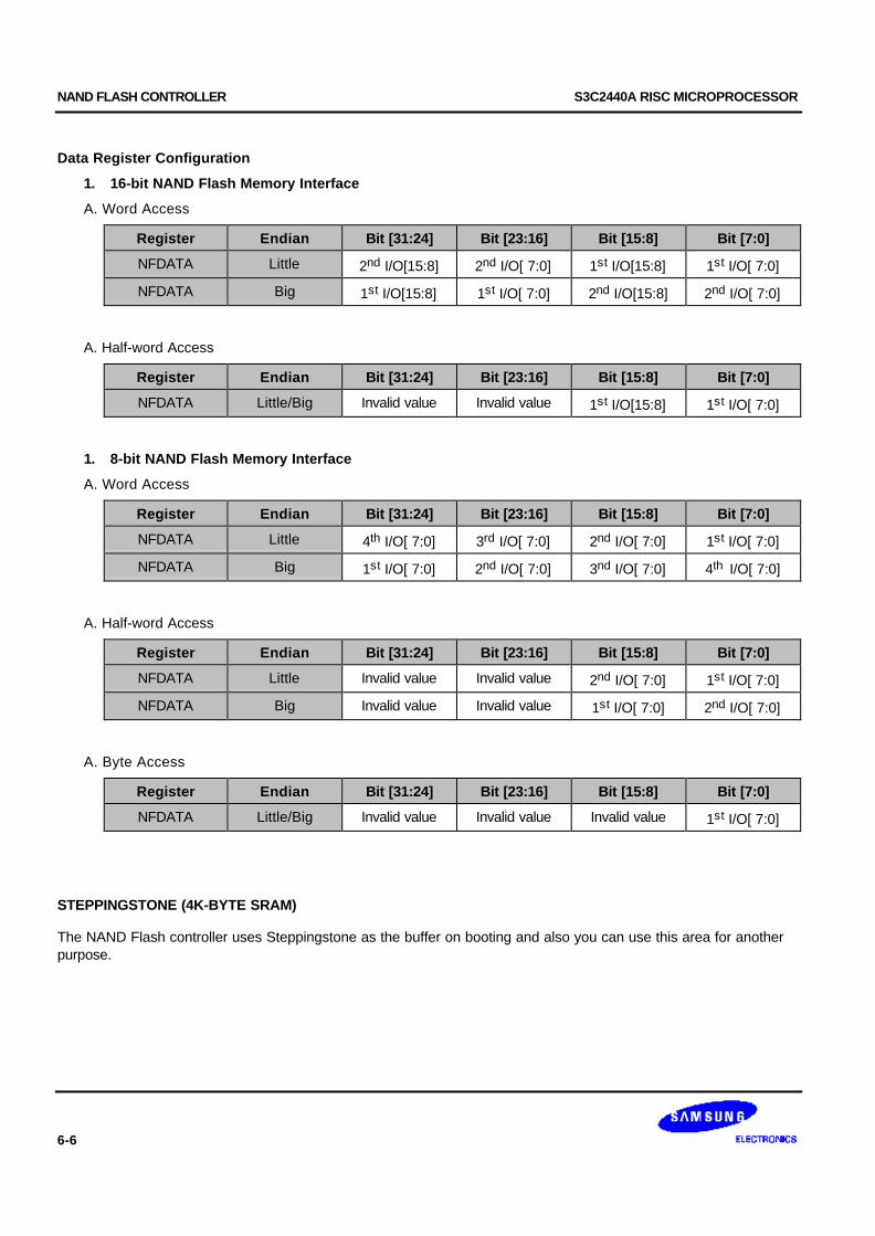
NAND FLASH CONTROLLER S3C2440A RISC MICROPROCESSOR
6-6
Data Register Configuration
1. 16-bit NAND Flash Memory Interface
A. Word Access
Register Endian Bit [31:24] Bit [23:16] Bit [15:8] Bit [7:0]
NFDATA Little 2nd I/O[15:8] 2nd I/O[ 7:0] 1st I/O[15:8] 1st I/O[ 7:0]
NFDATA Big 1st I/O[15:8] 1st I/O[ 7:0] 2nd I/O[15:8] 2nd I/O[ 7:0]
A. Half-word Access
Register Endian Bit [31:24] Bit [23:16] Bit [15:8] Bit [7:0]
NFDATA Little/Big Invalid value Invalid value 1st I/O[15:8] 1st I/O[ 7:0]
1. 8-bit NAND Flash Memory Interface
A. Word Access
Register Endian Bit [31:24] Bit [23:16] Bit [15:8] Bit [7:0]
NFDATA Little 4th I/O[ 7:0] 3rd I/O[ 7:0] 2nd I/O[ 7:0] 1st I/O[ 7:0]
NFDATA Big 1st I/O[ 7:0] 2nd I/O[ 7:0] 3nd I/O[ 7:0] 4th I/O[ 7:0]
A. Half-word Access
Register Endian Bit [31:24] Bit [23:16] Bit [15:8] Bit [7:0]
NFDATA Little Invalid value Invalid value 2nd I/O[ 7:0] 1st I/O[ 7:0]
NFDATA Big Invalid value Invalid value 1st I/O[ 7:0] 2nd I/O[ 7:0]
A. Byte Access
Register Endian Bit [31:24] Bit [23:16] Bit [15:8] Bit [7:0]
NFDATA Little/Big Invalid value Invalid value Invalid value 1st I/O[ 7:0]
STEPPINGSTONE (4K-BYTE SRAM)
The NAND Flash controller uses Steppingstone as the buffer on booting and also you can use this area for anotherpurpose.
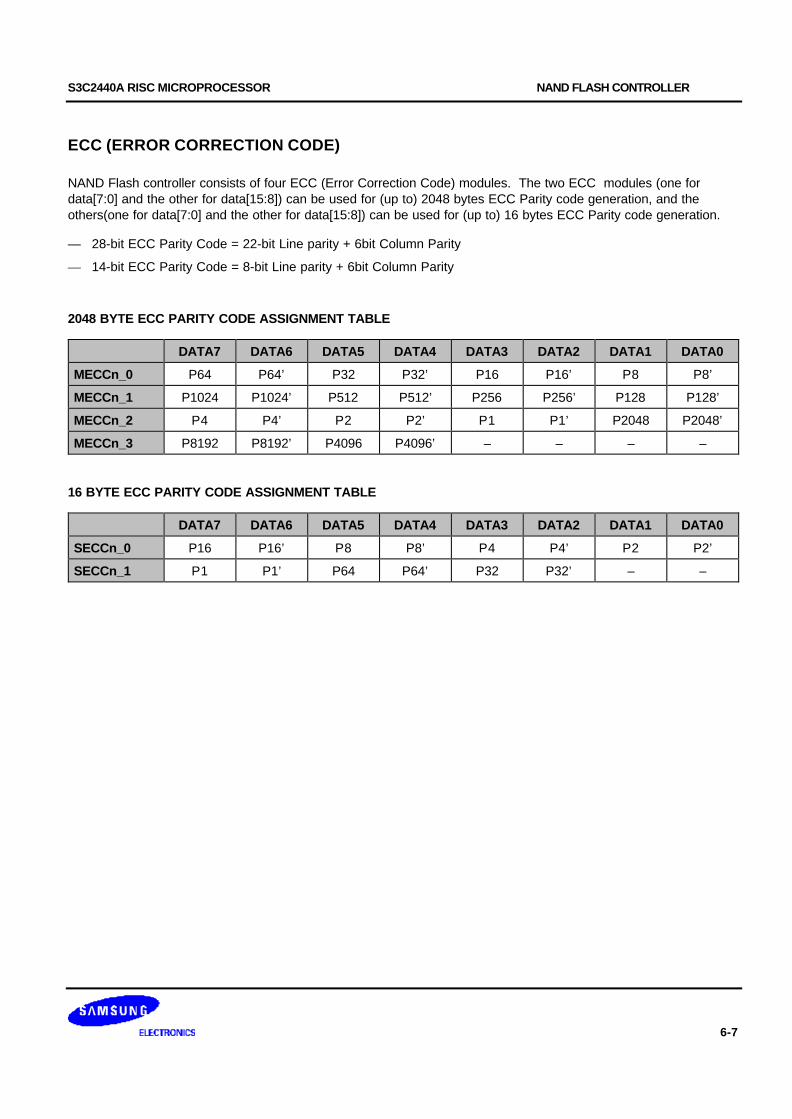
S3C2440A RISC MICROPROCESSOR NAND FLASH CONTROLLER
6-7
ECC (ERROR CORRECTION CODE)
NAND Flash controller consists of four ECC (Error Correction Code) modules. The two ECC modules (one fordata[7:0] and the other for data[15:8]) can be used for (up to) 2048 bytes ECC Parity code generation, and theothers(one for data[7:0] and the other for data[15:8]) can be used for (up to) 16 bytes ECC Parity code generation.
— 28-bit ECC Parity Code = 22-bit Line parity + 6bit Column Parity
— 14-bit ECC Parity Code = 8-bit Line parity + 6bit Column Parity
2048 BYTE ECC PARITY CODE ASSIGNMENT TABLE
DATA7 DATA6 DATA5 DATA4 DATA3 DATA2 DATA1 DATA0
MECCn_0 P64 P64’ P32 P32’ P16 P16’ P8 P8’
MECCn_1 P1024 P1024’ P512 P512’ P256 P256’ P128 P128’
MECCn_2 P4 P4’ P2 P2’ P1 P1’ P2048 P2048’
MECCn_3 P8192 P8192’ P4096 P4096’ – – – –
16 BYTE ECC PARITY CODE ASSIGNMENT TABLE
DATA7 DATA6 DATA5 DATA4 DATA3 DATA2 DATA1 DATA0
SECCn_0 P16 P16’ P8 P8’ P4 P4’ P2 P2’
SECCn_1 P1 P1’ P64 P64’ P32 P32’ – –
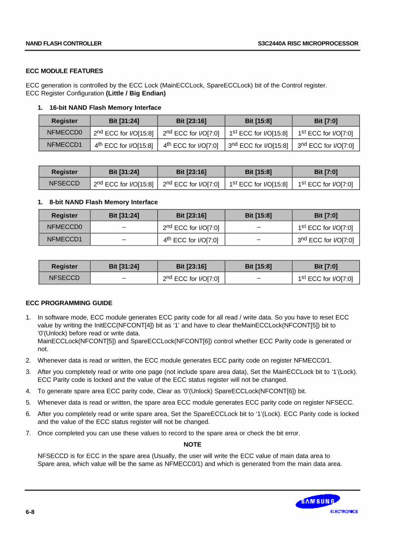
NAND FLASH CONTROLLER S3C2440A RISC MICROPROCESSOR
6-8
ECC MODULE FEATURES
ECC generation is controlled by the ECC Lock (MainECCLock, SpareECCLock) bit of the Control register.ECC Register Configuration (Little / Big Endian)
1. 16-bit NAND Flash Memory Interface
Register Bit [31:24] Bit [23:16] Bit [15:8] Bit [7:0]
NFMECCD0 2nd ECC for I/O[15:8] 2nd ECC for I/O[7:0] 1st ECC for I/O[15:8] 1st ECC for I/O[7:0]
NFMECCD1 4th ECC for I/O[15:8] 4th ECC for I/O[7:0] 3nd ECC for I/O[15:8] 3nd ECC for I/O[7:0]
Register Bit [31:24] Bit [23:16] Bit [15:8] Bit [7:0]
NFSECCD 2nd ECC for I/O[15:8] 2nd ECC for I/O[7:0] 1st ECC for I/O[15:8] 1st ECC for I/O[7:0]
1. 8-bit NAND Flash Memory Interface
Register Bit [31:24] Bit [23:16] Bit [15:8] Bit [7:0]
NFMECCD0 – 2nd ECC for I/O[7:0] – 1st ECC for I/O[7:0]
NFMECCD1 – 4th ECC for I/O[7:0] – 3nd ECC for I/O[7:0]
Register Bit [31:24] Bit [23:16] Bit [15:8] Bit [7:0]
NFSECCD – 2nd ECC for I/O[7:0] – 1st ECC for I/O[7:0]
ECC PROGRAMMING GUIDE
1. In software mode, ECC module generates ECC parity code for all read / write data. So you have to reset ECCvalue by writing the InitECC(NFCONT[4]) bit as ‘1’ and have to clear theMainECCLock(NFCONT[5]) bit to‘0’(Unlock) before read or write data.MainECCLock(NFCONT[5]) and SpareECCLock(NFCONT[6]) control whether ECC Parity code is generated ornot.
2. Whenever data is read or written, the ECC module generates ECC parity code on register NFMECC0/1.
3. After you completely read or write one page (not include spare area data), Set the MainECCLock bit to ‘1’(Lock).ECC Parity code is locked and the value of the ECC status register will not be changed.
4. To generate spare area ECC parity code, Clear as ‘0’(Unlock) SpareECCLock(NFCONT[6]) bit.
5. Whenever data is read or written, the spare area ECC module generates ECC parity code on register NFSECC.
6. After you completely read or write spare area, Set the SpareECCLock bit to ‘1’(Lock). ECC Parity code is lockedand the value of the ECC status register will not be changed.
7. Once completed you can use these values to record to the spare area or check the bit error.
NOTE
NFSECCD is for ECC in the spare area (Usually, the user will write the ECC value of main data area toSpare area, which value will be the same as NFMECC0/1) and which is generated from the main data area.
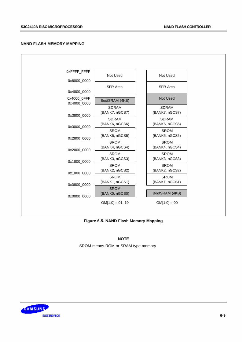
S3C2440A RISC MICROPROCESSOR NAND FLASH CONTROLLER
6-9
NAND FLASH MEMORY MAPPING
Not Used
SFR Area
Not Used
BootSRAM (4KB)
0xFFFF_FFFF
0x6000_0000
0x4800_0000
0x4000_0000
SFR Area
Not Used
SDRAM(BANK7, nGCS7)
0x3800_0000
SDRAM(BANK7, nGCS7)
SDRAM(BANK6, nGCS6)
0x3000_0000
SDRAM(BANK6, nGCS6)
SROM(BANK5, nGCS5)
SROM(BANK5, nGCS5)
0x2000_0000
0x2800_0000SROM
(BANK4, nGCS4)
SROM(BANK3, nGCS3)
SROM(BANK2, nGCS2)
0x1000_0000
0x1800_0000
0x0800_0000
SROM(BANK1, nGCS1)
SROM(BANK4, nGCS4)
SROM(BANK3, nGCS3)
SROM(BANK2, nGCS2)
SROM(BANK1, nGCS1)
SROM(BANK0, nGCS0) BootSRAM (4KB)
0x0000_0000
OM[1:0] = 01, 10 OM[1:0] = 00
0x4000_0FFF
Figure 6-5. NAND Flash Memory Mapping
NOTE
SROM means ROM or SRAM type memory
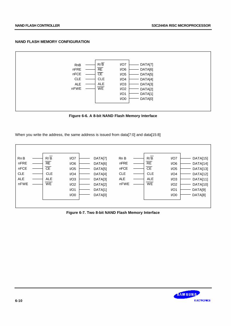
NAND FLASH CONTROLLER S3C2440A RISC MICROPROCESSOR
6-10
NAND FLASH MEMORY CONFIGURATION
I/O7I/O6I/O5I/O4I/O3I/O2I/O1I/O0
R/B
WEALECLECERE
RnB
nFWEALECLE
nFCEnFRE
DATA[7]DATA[6]DATA[5]DATA[4]DATA[3]DATA[2]DATA[1]DATA[0]
Figure 6-6. A 8-bit NAND Flash Memory Interface
When you write the address, the same address is issued from data[7:0] and data[15:8]
I/O7I/O6I/O5I/O4I/O3I/O2I/O1I/O0
R/ B
WEALECLECERE
Rn B
nFWEALECLEnFCEnFRE
DATA[7]DATA[6]DATA[5]DATA[4]DATA[3]DATA[2]DATA[1]DATA[0]
I/O7I/O6I/O5I/O4I/O3I/O2I/O1I/O0
R/B
WEALECLECERE
Rn B
nFWEALECLEnFCEnFRE
DATA[15]DATA[14]DATA[13]DATA[12]DATA[11]DATA[10]DATA[9]DATA[8]
Figure 6-7. Two 8-bit NAND Flash Memory Interface
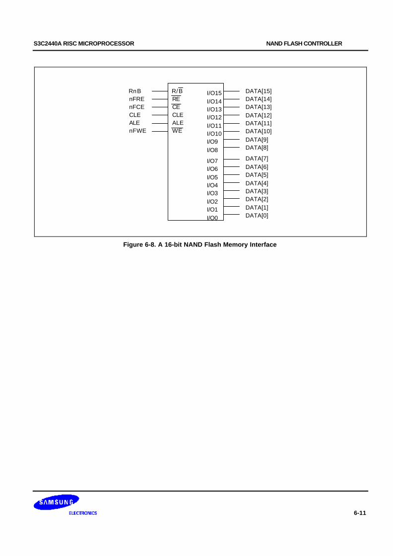
S3C2440A RISC MICROPROCESSOR NAND FLASH CONTROLLER
6-11
I/O15I/O14I/O13I/O12I/O11I/O10I/O9I/O8
R/B
WEALECLECERE
I/O7I/O6I/O5I/O4I/O3I/O2I/O1I/O0
RnB
nFWEALECLEnFCEnFRE
DATA[7]DATA[6]DATA[5]DATA[4]DATA[3]DATA[2]DATA[1]DATA[0]
DATA[15]DATA[14]DATA[13]DATA[12]DATA[11]DATA[10]DATA[9]DATA[8]
Figure 6-8. A 16-bit NAND Flash Memory Interface

NAND FLASH CONTROLLER S3C2440A RISC MICROPROCESSOR
6-12
NAND FLASH CONFIGURATION REGISTER
Register Address R/W Description Reset Value
NFCONF 0x4E000000 R/W NAND flash configuration register 0x0000100X
NFCONF Bit Description Initial StateReserved [15:14] Reserved –TACLS [13:12] CLE & ALE duration setting value (0~3)
Duration = HCLK x TACLS01
Reserved [11] Reserved 0TWRPH0 [10:8] TWRPH0 duration setting value (0~7)
Duration = HCLK x ( TWRPH0 + 1 )000
Reserved [7] Reserved 0TWRPH1 [6:4] TWRPH1 duration setting value (0~7)
Duration = HCLK x ( TWRPH1 + 1 )000
AdvFlash (Read only) [3] Advance NAND flash memory for auto-booting0: Support 256 or 512 byte/page NAND flash memory1: Support 1024 or 2048 byte/page NAND flash memoryThis bit is determined by NCON0 pin status during resetand wake-up from sleep mode.
H/W Set(NCON0)
PageSize (Read only) [2] NAND flash memory page size for auto-booting AdvFlashPageSizeWhen AdvFlash is 0,0: 256 Word/page, 1: 512 Bytes/pageWhen AdvFlash is 1,0: 1024 Word/page, 1: 2048 Bytes/pageThis bit is determined by GPG13 pin status during resetand wake-up from sleep mode. After reset, the GPG13 canbe used as general I/O port or External interrupt.
H/W Set(GPG13)
AddrCycle (Read only) [1] NAND flash memory Address cycle for auto-bootingAdvFlash AddrCycleWhen AdvFlash is 0,0: 3 address cycle 1: 4 address cycleWhen AdvFlash is 1,0: 4 address cycle 1: 5 address cycleThis bit is determined by GPG14pin status during resetand wake-up from sleep mode. After reset, the GPG14canbe used as general I/O port or External interrupt.
H/W Set(GPG14)
BusWidth (R/W) [0] NAND Flash Memory I/O bus width for auto-booting andgeneral access.0: 8-bit bus 1: 16-bit busThis bit is determined by GPG15 pin status during resetand wake-up from sleep mode.After reset, the GPG15 can be used as general I/O port orExternal interrupt.This bit can be changed by software.
H/W Set(GPG15)
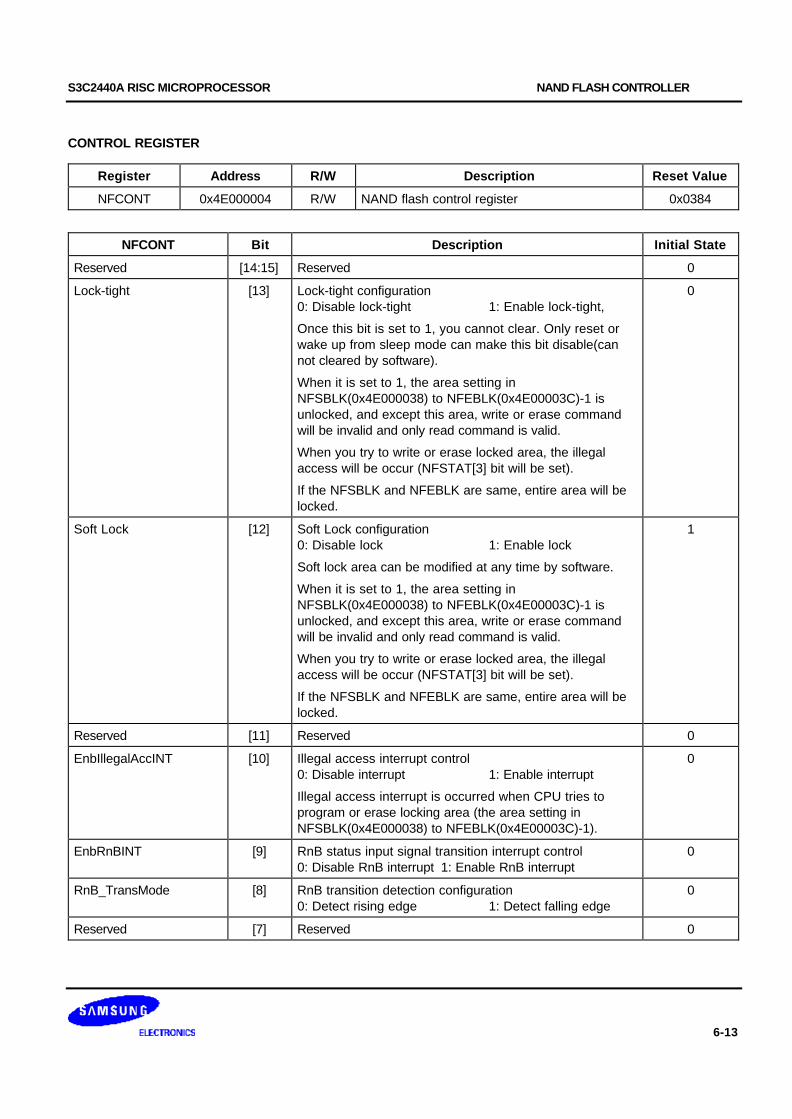
S3C2440A RISC MICROPROCESSOR NAND FLASH CONTROLLER
6-13
CONTROL REGISTER
Register Address R/W Description Reset Value
NFCONT 0x4E000004 R/W NAND flash control register 0x0384
NFCONT Bit Description Initial State
Reserved [14:15] Reserved 0
Lock-tight [13] Lock-tight configuration0: Disable lock-tight 1: Enable lock-tight,
Once this bit is set to 1, you cannot clear. Only reset orwake up from sleep mode can make this bit disable(cannot cleared by software).
When it is set to 1, the area setting inNFSBLK(0x4E000038) to NFEBLK(0x4E00003C)-1 isunlocked, and except this area, write or erase commandwill be invalid and only read command is valid.
When you try to write or erase locked area, the illegalaccess will be occur (NFSTAT[3] bit will be set).
If the NFSBLK and NFEBLK are same, entire area will belocked.
0
Soft Lock [12] Soft Lock configuration0: Disable lock 1: Enable lock
Soft lock area can be modified at any time by software.
When it is set to 1, the area setting inNFSBLK(0x4E000038) to NFEBLK(0x4E00003C)-1 isunlocked, and except this area, write or erase commandwill be invalid and only read command is valid.
When you try to write or erase locked area, the illegalaccess will be occur (NFSTAT[3] bit will be set).
If the NFSBLK and NFEBLK are same, entire area will belocked.
1
Reserved [11] Reserved 0
EnbIllegalAccINT [10] Illegal access interrupt control0: Disable interrupt 1: Enable interrupt
Illegal access interrupt is occurred when CPU tries toprogram or erase locking area (the area setting inNFSBLK(0x4E000038) to NFEBLK(0x4E00003C)-1).
0
EnbRnBINT [9] RnB status input signal transition interrupt control0: Disable RnB interrupt 1: Enable RnB interrupt
0
RnB_TransMode [8] RnB transition detection configuration0: Detect rising edge 1: Detect falling edge
0
Reserved [7] Reserved 0
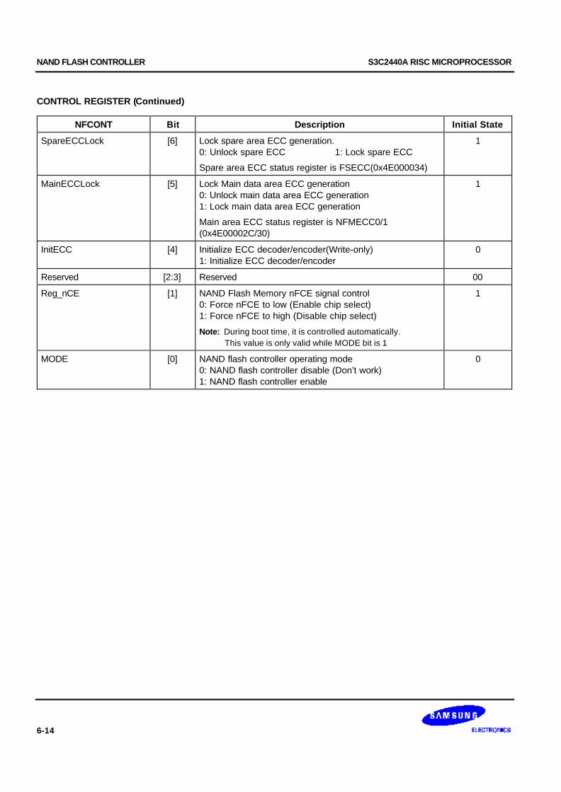
NAND FLASH CONTROLLER S3C2440A RISC MICROPROCESSOR
6-14
CONTROL REGISTER (Continued)
NFCONT Bit Description Initial State
SpareECCLock [6] Lock spare area ECC generation.0: Unlock spare ECC 1: Lock spare ECC
Spare area ECC status register is FSECC(0x4E000034)
1
MainECCLock [5] Lock Main data area ECC generation0: Unlock main data area ECC generation1: Lock main data area ECC generation
Main area ECC status register is NFMECC0/1(0x4E00002C/30)
1
InitECC [4] Initialize ECC decoder/encoder(Write-only)1: Initialize ECC decoder/encoder
0
Reserved [2:3] Reserved 00
Reg_nCE [1] NAND Flash Memory nFCE signal control0: Force nFCE to low (Enable chip select)1: Force nFCE to high (Disable chip select)
Note: During boot time, it is controlled automatically. This value is only valid while MODE bit is 1
1
MODE [0] NAND flash controller operating mode0: NAND flash controller disable (Don’t work)1: NAND flash controller enable
0
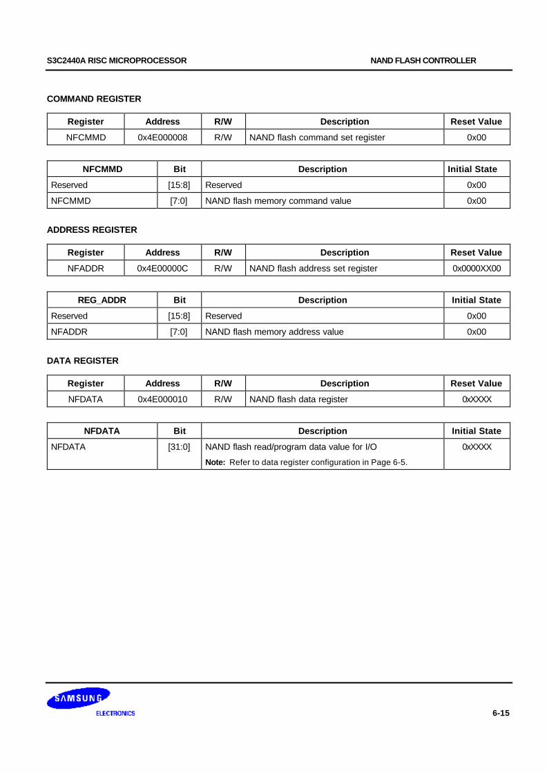
S3C2440A RISC MICROPROCESSOR NAND FLASH CONTROLLER
6-15
COMMAND REGISTER
Register Address R/W Description Reset Value
NFCMMD 0x4E000008 R/W NAND flash command set register 0x00
NFCMMD Bit Description Initial State
Reserved [15:8] Reserved 0x00
NFCMMD [7:0] NAND flash memory command value 0x00
ADDRESS REGISTER
Register Address R/W Description Reset Value
NFADDR 0x4E00000C R/W NAND flash address set register 0x0000XX00
REG_ADDR Bit Description Initial State
Reserved [15:8] Reserved 0x00
NFADDR [7:0] NAND flash memory address value 0x00
DATA REGISTER
Register Address R/W Description Reset Value
NFDATA 0x4E000010 R/W NAND flash data register 0xXXXX
NFDATA Bit Description Initial State
NFDATA [31:0] NAND flash read/program data value for I/O
Note: Refer to data register configuration in Page 6-5.
0xXXXX
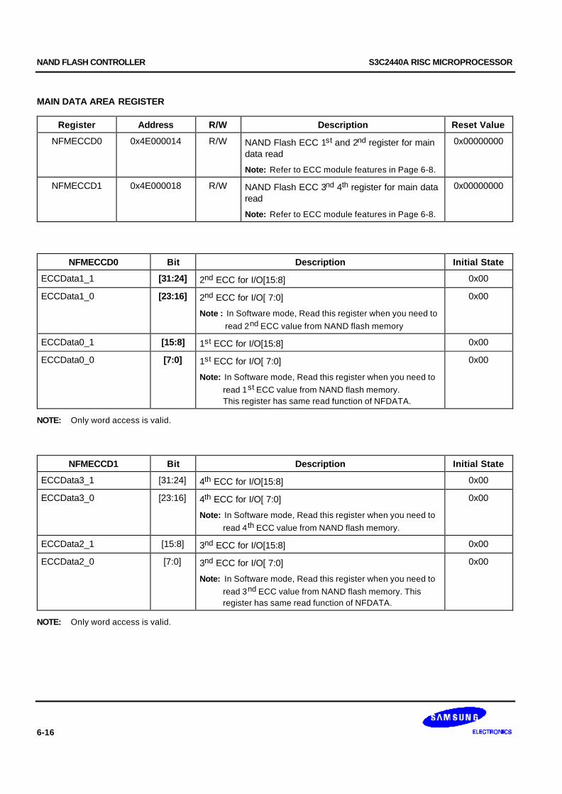
NAND FLASH CONTROLLER S3C2440A RISC MICROPROCESSOR
6-16
MAIN DATA AREA REGISTER
Register Address R/W Description Reset Value
NFMECCD0 0x4E000014 R/W NAND Flash ECC 1st and 2nd register for maindata read
Note: Refer to ECC module features in Page 6-8.
0x00000000
NFMECCD1 0x4E000018 R/W NAND Flash ECC 3nd 4th register for main dataread
Note: Refer to ECC module features in Page 6-8.
0x00000000
NFMECCD0 Bit Description Initial State
ECCData1_1 [31:24] 2nd ECC for I/O[15:8] 0x00
ECCData1_0 [23:16] 2nd ECC for I/O[ 7:0]
Note : In Software mode, Read this register when you need to read 2nd ECC value from NAND flash memory
0x00
ECCData0_1 [15:8] 1st ECC for I/O[15:8] 0x00
ECCData0_0 [7:0] 1st ECC for I/O[ 7:0]
Note: In Software mode, Read this register when you need to read 1st ECC value from NAND flash memory. This register has same read function of NFDATA.
0x00
NOTE: Only word access is valid.
NFMECCD1 Bit Description Initial State
ECCData3_1 [31:24] 4th ECC for I/O[15:8] 0x00
ECCData3_0 [23:16] 4th ECC for I/O[ 7:0]
Note: In Software mode, Read this register when you need to read 4 th ECC value from NAND flash memory.
0x00
ECCData2_1 [15:8] 3nd ECC for I/O[15:8] 0x00
ECCData2_0 [7:0] 3nd ECC for I/O[ 7:0]
Note: In Software mode, Read this register when you need to read 3nd ECC value from NAND flash memory. This register has same read function of NFDATA.
0x00
NOTE: Only word access is valid.

S3C2440A RISC MICROPROCESSOR NAND FLASH CONTROLLER
6-17
SPARE AREA ECC REGISTER
Register Address R/W Description Reset Value
NFSECCD 0x4E00001C R/W NAND flash ECC (Error Correction Code)register for spare area data read
0x00000000
NFSECCD Bit Description Initial State
ECCData1_1 [31:24] 2nd ECC for I/O[15:8] 0x00
ECCData1_0 [23:16] 2nd ECC for I/O[ 7:0]
Note: In Software mode, Read this register when you need to read 2nd ECC value from NAND flash memory.
0x00
ECCData0_1 [15:8] 1st ECC for I/O[15:8] 0x00
ECCData0_0 [7:0] 1st ECC for I/O[ 7:0]
Note: In Software mode, Read this register when you need to read 1st ECC value from NAND flash memory. This register has same read function of NFDATA.
0x00
NOTE: Only word access is valid.
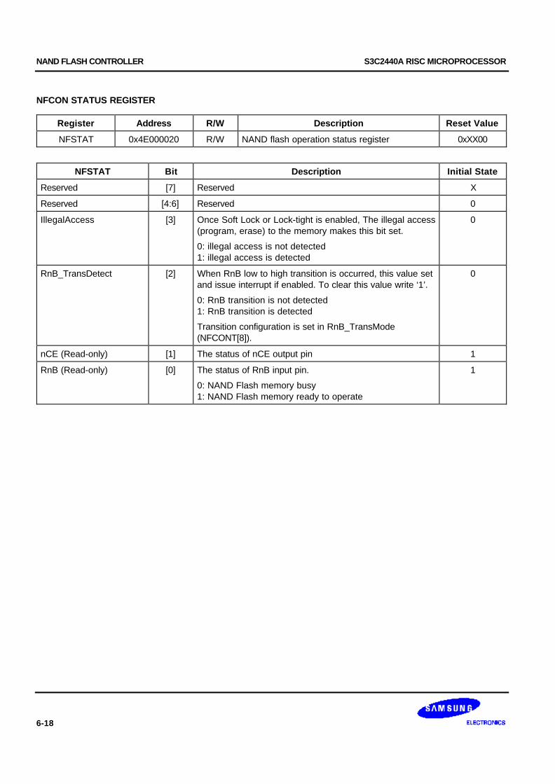
NAND FLASH CONTROLLER S3C2440A RISC MICROPROCESSOR
6-18
NFCON STATUS REGISTER
Register Address R/W Description Reset Value
NFSTAT 0x4E000020 R/W NAND flash operation status register 0xXX00
NFSTAT Bit Description Initial State
Reserved [7] Reserved X
Reserved [4:6] Reserved 0
IllegalAccess [3] Once Soft Lock or Lock-tight is enabled, The illegal access(program, erase) to the memory makes this bit set.
0: illegal access is not detected1: illegal access is detected
0
RnB_TransDetect [2] When RnB low to high transition is occurred, this value setand issue interrupt if enabled. To clear this value write ‘1’.
0: RnB transition is not detected1: RnB transition is detected
Transition configuration is set in RnB_TransMode(NFCONT[8]).
0
nCE (Read-only) [1] The status of nCE output pin 1
RnB (Read-only) [0] The status of RnB input pin.
0: NAND Flash memory busy1: NAND Flash memory ready to operate
1

S3C2440A RISC MICROPROCESSOR NAND FLASH CONTROLLER
6-19
ECC0/1 STATUS REGISTER
Register Address R/W Description Reset Value
NFESTAT0 0x4E000024 R/W NAND flash ECC Status register for I/O [7:0] 0x00000000
NFESTAT1 0x4E000028 R/W NAND flash ECC status register for I/O [15:8] 0x00000000
NFESTAT0 Bit Description Initial State
SErrorDataNo [24:21] In spare area, Indicates which number data is error 00
SErrorBitNo [20:18] In spare area, Indicates which bit is error 000
MErrorDataNo [17:7] In main data area, Indicates which number data is error 0x00
MErrorBitNo [6:4] In main data area, Indicates which bit is error 000
SpareError [3:2] Indicates whether spare area bit fail error occurred
00: No Error 01: 1-bit error(correctable)10: Multiple error 11: ECC area error
00
MainError [1:0] Indicates whether main data area bit fail error occurred
00: No Error 01: 1-bit error(correctable)10: Multiple error 11: ECC area error
00
NOTE: The above values are only valid when both ECC register and ECC status register have valid value.
NFESTAT1 Bit Description Initial State
SErrorDataNo [24:21] In spare area, Indicates which number data is error 00
SErrorBitNo [20:18] In spare area, Indicates which bit is error 000
MErrorDataNo [17:7] In main data area, Indicates which number data is error 0x00
MErrorBitNo [6:4] In main data area, Indicates which bit is error 000
SpareError [3:2] Indicates whether spare area bit fail error occurred
00: No Error 01: 1-bit error(correctable)10: Multiple error 11: ECC area error
00
MainError [1:0] Indicates whether main data area bit fail error occurred
00: No Error 01: 1-bit error(correctable)10: Multiple error 11: ECC area error
00
NOTE: The above values are only valid when both ECC register and ECC status register have valid value.
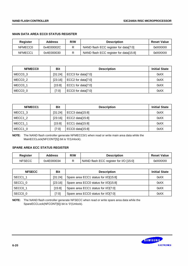
NAND FLASH CONTROLLER S3C2440A RISC MICROPROCESSOR
6-20
MAIN DATA AREA ECC0 STATUS REGISTER
Register Address R/W Description Reset Value
NFMECC0 0x4E00002C R NAND flash ECC register for data[7:0] 0xXXXXXX
NFMECC1 0x4E000030 R NAND flash ECC register for data[15:8] 0xXXXXXX
NFMECC0 Bit Description Initial State
MECC0_3 [31:24] ECC3 for data[7:0] 0xXX
MECC0_2 [23:16] ECC2 for data[7:0] 0xXX
MECC0_1 [15:8] ECC1 for data[7:0] 0xXX
MECC0_0 [7:0] ECC0 for data[7:0] 0xXX
NFMECC1 Bit Description Initial State
MECC1_3 [31:24] ECC3 data[15:8] 0xXX
MECC1_2 [23:16] ECC2 data[15:8] 0xXX
MECC1_1 [15:8] ECC1 data[15:8] 0xXX
MECC1_0 [7:0] ECC0 data[15:8] 0xXX
NOTE: The NAND flash controller generate NFMECC0/1 when read or write main area data while the MainECCLock(NFCONT[5]) bit is ‘0’(Unlock).
SPARE AREA ECC STATUS REGISTER
Register Address R/W Description Reset Value
NFSECC 0x4E000034 R NAND flash ECC register for I/O [15:0] 0xXXXXXX
NFSECC Bit Description Initial State
SECC1_1 [31:24] Spare area ECC1 status for I/O[15:8] 0xXX
SECC1_0 [23:16] Spare area ECC0 status for I/O[15:8] 0xXX
SECC0_1 [15:8] Spare area ECC1 status for I/O[7:0] 0xXX
SECC0_0 [7:0] Spare area ECC0 status for I/O[7:0] 0xXX
NOTE: The NAND flash controller generate NFSECC when read or write spare area data while the SpareECCLock(NFCONT[6]) bit is ‘0’(Unlock).

S3C2440A RISC MICROPROCESSOR NAND FLASH CONTROLLER
6-21
BLOCK ADDRESS REGISTER
Register Address R/W Description Reset Value
NFSBLK 0x4E000038 R/W NAND flash programmable start block address 0x000000
NFEBLK 0x4E00003C R/W NAND flash programmable end block address
Nand Flash can be programmed between startand end address.
When the soft lock or lock-tight is enabled andthe start and end address has same value,Entire area of NAND flash will be locked.
0x000000
NFSBLK Bit Description Initial State
SBLK_ADDR2 [23:16] The 3nd block address of the block erase operation 0x00
SBLK_ADDR1 [15:8] The 2nd block address of the block erase operation 0x00
SBLK_ADDR0 [7:0] The 1st block address of the block erase operation(Only bit [7:5] are valid)
0x00
NOTE: Advance Flash’s block Address start from 3-address cycle. So block address register only needs 3-bytes.
NFEBLK Bit Description Initial State
EBLK_ADDR2 [23:16] The 3rd block address of the block erase operation 0x00
EBLK_ADDR1 [15:8] The 2nd block address of the block erase operation 0x00
EBLK_ADDR0 [7:0] The 1st block address of the block erase operation(Only bit [7:5] are valid)
0x00
NOTE: Advance Flash’s block Address start from 3-address cycle. So block address register only needs 3-bytes.
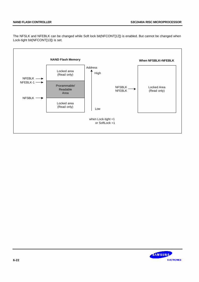
NAND FLASH CONTROLLER S3C2440A RISC MICROPROCESSOR
6-22
The NFSLK and NFEBLK can be changed while Soft lock bit(NFCONT[12]) is enabled. But cannot be changed whenLock-tight bit(NFCONT[13]) is set.
when Lock-tight =1 or SoftLock =1
NAND Flash Memory
Locked area(Read only)
Prorammable/Readable
Area
Locked area(Read only)
NFSBLK
Address
High
Low
NFEBLKNFEBLK-1
NFSBLKNFEBLK
Locked Area(Read only)
When NFSBLK=NFEBLK

S3C2440A RISC MICROPROCESSOR CLOCK & POWER MANAGEMENT
7-1
7 CLOCK & POWER MANAGEMENT
OVERVIEW
The Clock & Power management block consists of three parts: Clock control, USB control, and Power control.
The Clock control logic in S3C2440A can generate the required clock signals including FCLK for CPU, HCLK for theAHB bus peripherals, and PCLK for the APB bus peripherals. The S3C2440A has two Phase Locked Loops (PLLs):one for FCLK, HCLK, and PCLK, and the other dedicated for USB block (48Mhz). The clock control logic can makeslow clocks without PLL and connect/disconnect the clock to each peripheral block by software, which will reducethe power consumption.
For the power control logic, the S3C2440A has various power management schemes to keep optimal powerconsumption for a given task. The power management block in the S3C2440A can activate four modes: NORMALmode, SLOW mode, IDLE mode, and SLEEP mode.
NORMAL mode: The block supplies clocks to CPU as well as all peripherals in the S3C2440A. In this mode, thepower consumption will be maximized when all peripherals are turned on. It allows the user to control the operation ofperipherals by software. For example, if a timer is not needed, the user can disconnect the clock(CLKCON register)to the timer to reduce power consumption.
SLOW mode: Non-PLL mode. Unlike the Normal mode, the Slow mode uses an external clock (XTIpll or EXTCLK)directly as FCLK in the S3C2440A without PLL. In this mode, the power consumption depends on the frequency ofthe external clock only. The power consumption due to PLL is excluded.
IDLE mode: The block disconnects clocks (FCLK) only to the CPU core while it supplies clocks to all otherperipherals. The IDLE mode results in reduced power consumption due to CPU core. Any interrupt request to CPUcan be woken up from the Idle mode.
SLEEP mode: The block disconnects the internal power. So, there occurs no power consumption due to CPU andthe internal logic except the wake-up logic in this mode. Activating the SLEEP mode requires two independent powersources. One of the two power sources supplies the power for the wake-up logic. The other one supplies otherinternal logics including CPU, and should be controlled for power on/off. In the SLEEP mode, the second powersupply source for the CPU and internal logics will be turned off. The wakeup from SLEEP mode can be issued by theEINT[15:0] or by RTC alarm interrupt.
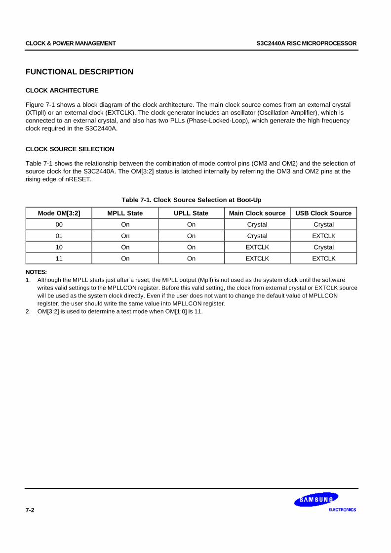
CLOCK & POWER MANAGEMENT S3C2440A RISC MICROPROCESSOR
7-2
FUNCTIONAL DESCRIPTION
CLOCK ARCHITECTURE
Figure 7-1 shows a block diagram of the clock architecture. The main clock source comes from an external crystal(XTIpll) or an external clock (EXTCLK). The clock generator includes an oscillator (Oscillation Amplifier), which isconnected to an external crystal, and also has two PLLs (Phase-Locked-Loop), which generate the high frequencyclock required in the S3C2440A.
CLOCK SOURCE SELECTION
Table 7-1 shows the relationship between the combination of mode control pins (OM3 and OM2) and the selection ofsource clock for the S3C2440A. The OM[3:2] status is latched internally by referring the OM3 and OM2 pins at therising edge of nRESET.
Table 7-1. Clock Source Selection at Boot-Up
Mode OM[3:2] MPLL State UPLL State Main Clock source USB Clock Source
00 On On Crystal Crystal
01 On On Crystal EXTCLK
10 On On EXTCLK Crystal
11 On On EXTCLK EXTCLK
NOTES:1. Although the MPLL starts just after a reset, the MPLL output (Mpll) is not used as the system clock until the software
writes valid settings to the MPLLCON register. Before this valid setting, the clock from external crystal or EXTCLK sourcewill be used as the system clock directly. Even if the user does not want to change the default value of MPLLCONregister, the user should write the same value into MPLLCON register.
2. OM[3:2] is used to determine a test mode when OM[1:0] is 11.
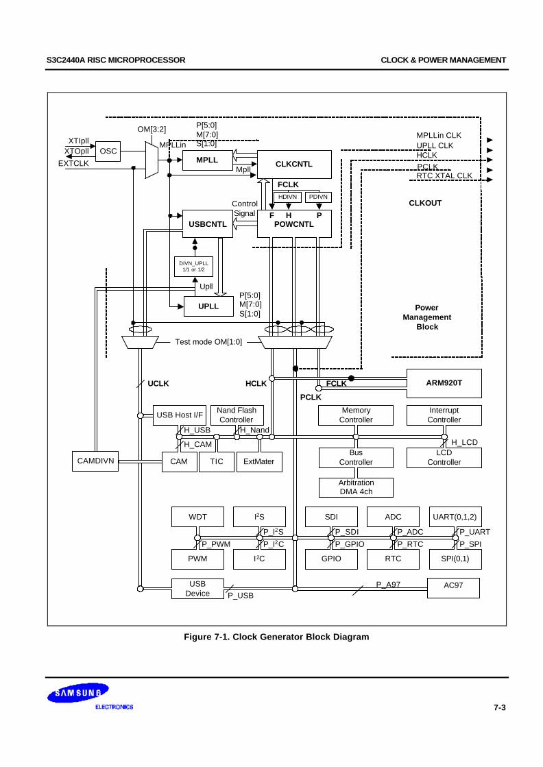
S3C2440A RISC MICROPROCESSOR CLOCK & POWER MANAGEMENT
7-3
Nand FlashController
OSCMPLL
UPLL
CLKCNTL
FCLKHDIVN PDIVN
Mpll
ControlSignal
Upll
POWCNTLF H P
USBCNTL
Test mode OM[1:0]
BusController
MemoryController
ArbitrationDMA 4ch
WDT I2S SDI ADC UART(0,1,2)
PWM I2C GPIO RTC SPI(0,1)
USBDevice
ARM920T
InterruptController
LCDController
H_LCD
P_SDI
P_GPIO
P_ADC
P_RTC
P_UART
P_SPI
P_I2S
P_I2CP_PWM
P_USB
H_Nand
FCLK
PCLK
HCLKUCLK
PowerManagement
Block
MPLLin CLKUPLL CLKHCLKPCLKRTC XTAL CLK
CLKOUT
XTIpllXTOpll
EXTCLK
P[5:0]M[7:0]S[1:0]
OM[3:2] P[5:0]M[7:0]S[1:0]
USB Host I/F
H_USB
TIC
H_CAM
CAM ExtMater
DIVN_UPLL1/1 or 1/2
CAMDIVN
P_A97 AC97
MPLLin
Figure 7-1. Clock Generator Block Diagram
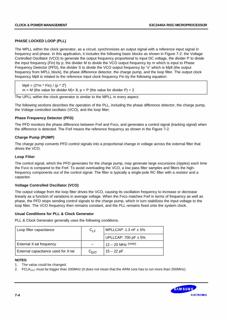
CLOCK & POWER MANAGEMENT S3C2440A RISC MICROPROCESSOR
7-4
PHASE LOCKED LOOP (PLL)
The MPLL within the clock generator, as a circuit, synchronizes an output signal with a reference input signal infrequency and phase. In this application, it includes the following basic blocks as shown in Figure 7-2: the VoltageControlled Oscillator (VCO) to generate the output frequency proportional to input DC voltage, the divider P to dividethe input frequency (Fin) by p, the divider M to divide the VCO output frequency by m which is input to PhaseFrequency Detector (PFD), the divider S to divide the VCO output frequency by “s” which is Mpll (the outputfrequency from MPLL block), the phase difference detector, the charge pump, and the loop filter. The output clockfrequency Mpll is related to the reference input clock frequency Fin by the following equation:
Mpll = (2*m * Fin) / (p * 2s) m = M (the value for divider M)+ 8, p = P (the value for divider P) + 2
The UPLL within the clock generator is similar to the MPLL in every aspect.
The following sections describes the operation of the PLL, including the phase difference detector, the charge pump,the Voltage controlled oscillator (VCO), and the loop filter.
Phase Frequency Detector (PFD)
The PFD monitors the phase difference between Fref and Fvco, and generates a control signal (tracking signal) whenthe difference is detected. The Fref means the reference frequency as shown in the Figure 7-2.
Charge Pump (PUMP)
The charge pump converts PFD control signals into a proportional change in voltage across the external filter thatdrives the VCO.
Loop Filter
The control signal, which the PFD generates for the charge pump, may generate large excursions (ripples) each timethe Fvco is compared to the Fref. To avoid overloading the VCO, a low pass filter samples and filters the high-frequency components out of the control signal. The filter is typically a single-pole RC filter with a resistor and acapacitor.
Voltage Controlled Oscillator (VCO)
The output voltage from the loop filter drives the VCO, causing its oscillation frequency to increase or decreaselinearly as a function of variations in average voltage. When the Fvco matches Fref in terms of frequency as well asphase, the PFD stops sending control signals to the charge pump, which in turn stabilizes the input voltage to theloop filter. The VCO frequency then remains constant, and the PLL remains fixed onto the system clock.
Usual Conditions for PLL & Clock Generator
PLL & Clock Generator generally uses the following conditions.
Loop filter capacitance CLF MPLLCAP: 1.3 nF ± 5%
UPLLCAP: 700 pF ± 5%
External X-tal frequency – 12 – 20 MHz (note)
External capacitance used for X-tal CEXT 15 – 22 pF
NOTES:1. The value could be changed.2. FCLKOUT must be bigger than 200MHz (It does not mean that the ARM core has to run more than 200MHz).
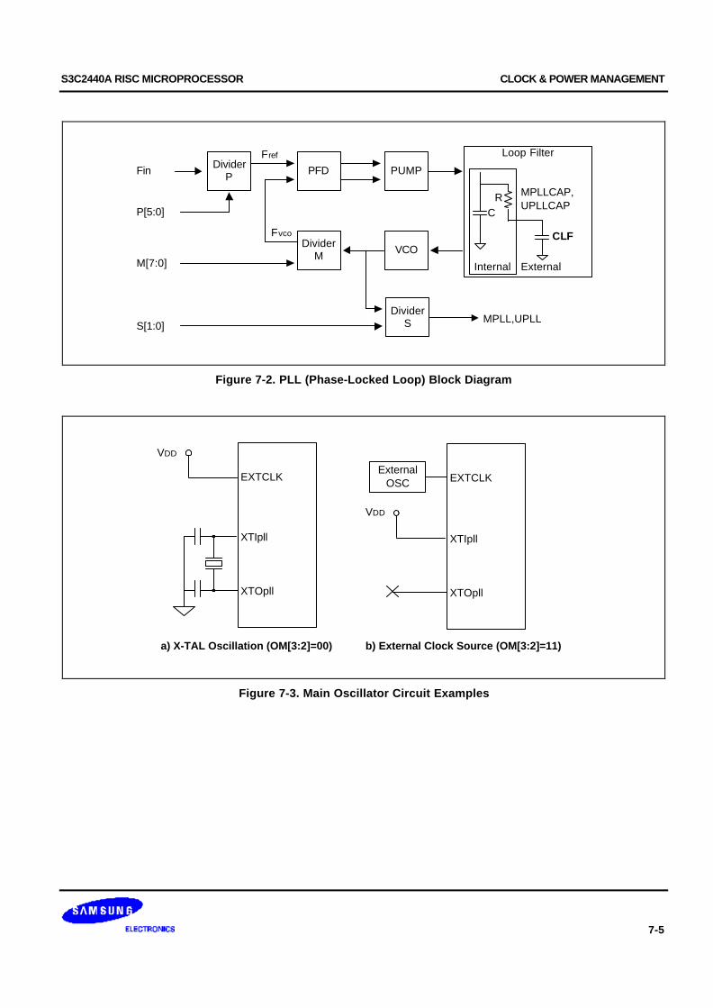
S3C2440A RISC MICROPROCESSOR CLOCK & POWER MANAGEMENT
7-5
DividerP
Loop Filter
Fin
M[7:0]
S[1:0]
PFD
DividerM
P[5:0]
Fvco
PUMP
VCO
DividerS
Fref
MPLL,UPLL
RC
Internal
CLF
External
MPLLCAP,UPLLCAP
Figure 7-2. PLL (Phase-Locked Loop) Block Diagram
EXTCLK
XTIpll
XTOpll
EXTCLK
XTIpll
XTOpll
ExternalOSC
a) X-TAL Oscillation (OM[3:2]=00) b) External Clock Source (OM[3:2]=11)
VDD
VDD
Figure 7-3. Main Oscillator Circuit Examples
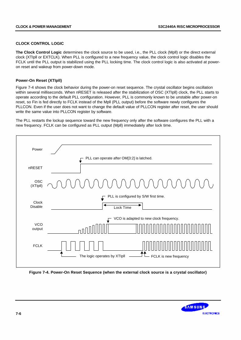
CLOCK & POWER MANAGEMENT S3C2440A RISC MICROPROCESSOR
7-6
CLOCK CONTROL LOGIC
The Clock Control Logic determines the clock source to be used, i.e., the PLL clock (Mpll) or the direct externalclock (XTIpll or EXTCLK). When PLL is configured to a new frequency value, the clock control logic disables theFCLK until the PLL output is stabilized using the PLL locking time. The clock control logic is also activated at power-on reset and wakeup from power-down mode.
Power-On Reset (XTIpll)
Figure 7-4 shows the clock behavior during the power-on reset sequence. The crystal oscillator begins oscillationwithin several milliseconds. When nRESET is released after the stabilization of OSC (XTIpll) clock, the PLL starts tooperate according to the default PLL configuration. However, PLL is commonly known to be unstable after power-onreset, so Fin is fed directly to FCLK instead of the Mpll (PLL output) before the software newly configures thePLLCON. Even if the user does not want to change the default value of PLLCON register after reset, the user shouldwrite the same value into PLLCON register by software.
The PLL restarts the lockup sequence toward the new frequency only after the software configures the PLL with anew frequency. FCLK can be configured as PLL output (Mpll) immediately after lock time.
The logic operates by XTIpll
nRESET
OSC(XTIpll)
VCOoutput
Power
ClockDisable Lock Time
PLL is configured by S/W first time.
VCO is adapted to new clock frequency.
FCLK
FCLK is new frequency
PLL can operate after OM[3:2] is latched.
Figure 7-4. Power-On Reset Sequence (when the external clock source is a crystal oscillator)
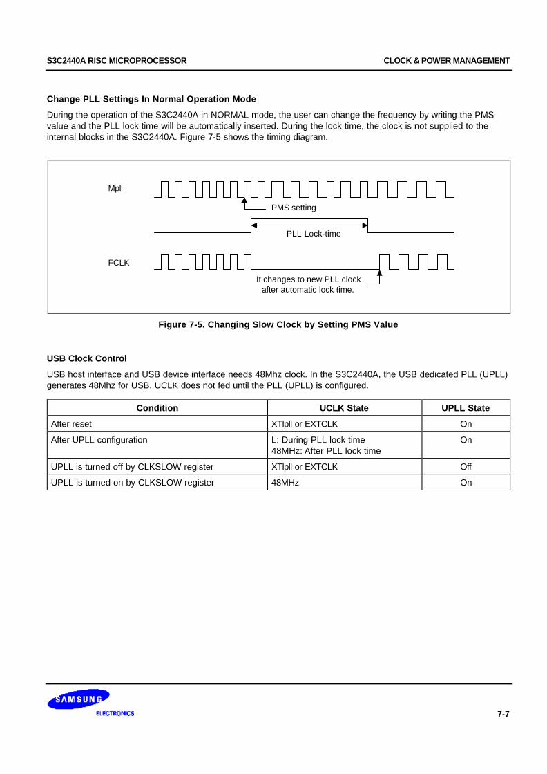
S3C2440A RISC MICROPROCESSOR CLOCK & POWER MANAGEMENT
7-7
Change PLL Settings In Normal Operation Mode
During the operation of the S3C2440A in NORMAL mode, the user can change the frequency by writing the PMSvalue and the PLL lock time will be automatically inserted. During the lock time, the clock is not supplied to theinternal blocks in the S3C2440A. Figure 7-5 shows the timing diagram.
Mpll
PMS setting
PLL Lock-time
FCLK
It changes to new PLL clockafter automatic lock time.
Figure 7-5. Changing Slow Clock by Setting PMS Value
USB Clock Control
USB host interface and USB device interface needs 48Mhz clock. In the S3C2440A, the USB dedicated PLL (UPLL)generates 48Mhz for USB. UCLK does not fed until the PLL (UPLL) is configured.
Condition UCLK State UPLL State
After reset XTlpll or EXTCLK On
After UPLL configuration L: During PLL lock time48MHz: After PLL lock time
On
UPLL is turned off by CLKSLOW register XTlpll or EXTCLK Off
UPLL is turned on by CLKSLOW register 48MHz On

CLOCK & POWER MANAGEMENT S3C2440A RISC MICROPROCESSOR
7-8
FCLK, HCLK, and PCLK
FCLK is used by ARM920T.HCLK is used for AHB bus, which is used by the ARM920T, the memory controller, the interrupt controller, the LCDcontroller, the DMA and USB host block.PCLK is used for APB bus, which is used by the peripherals such as WDT, IIS, I2C, PWM timer, MMC interface,ADC, UART, GPIO, RTC and SPI.
The S3C2440A supports selection of Dividing Ratio between FCLK, HLCK and PCLK. This ratio is determined byHDIVN and PDIVN of CLKDIVN control register.
HDIVN PDIVN HCLK3_HALF/HCLK4_HALF
FCLK HCLK PCLK Divide Ratio
0 0 – FCLK FCLK FCLK 1 : 1 : 1(Default)
0 1 – FCLK FCLK FCLK / 2 1 : 1 : 2
1 0 – FCLK FCLK / 2 FCLK / 2 1 : 2 : 2
1 1 – FCLK FCLK / 2 FCLK / 4 1 : 2 : 4
3 0 0 / 0 FCLK FCLK / 3 FCLK / 3 1 : 3 : 3
3 1 0 / 0 FCLK FCLK / 3 FCLK / 6 1 : 3 : 6
3 0 1 / 0 FCLK FCLK / 6 FCLK / 6 1 : 6 : 6
3 1 1 / 0 FCLK FCLK / 6 FCLK / 12 1 : 6 : 12
2 0 0 / 0 FCLK FCLK / 4 FCLK / 4 1 : 4 : 4
2 1 0 / 0 FCLK FCLK / 4 FCLK / 8 1 : 4 : 8
2 0 0 / 1 FCLK FCLK / 8 FCLK / 8 1 : 8 : 8
2 1 0 / 1 FCLK FCLK / 8 FCLK / 16 1 : 8 : 16
After setting PMS value, it is required to set CLKDIVN register. The value set for CLKDIVN will be valid after PLL locktime. The value is also available for reset and changing Power Management Mode.The setting value can also be valid after 1.5 HCLK. Only, 1HCLK can validate the value of CLKDIVN register changedfrom Default (1:1:1) to other Divide Ratio (1:1:2, 1:2:2, 1:2:4).
1 HCLK 1.5 HCLK 1.5 HCLK
0x00000000 0x00000001(1:1:2) 0x00000003 (1:2:4) 0x00000000 (1:1:1)CLKDIVN
FCLK
HCLK
PCLK
Figure 7-6. Example of Internal Clock Change
S3C2440A RISC MICROPROCESSOR CLOCK & POWER MANAGEMENT
7-9
NOTES
1. CLKDIVN should be set carefully not to exceed the limit of HCLK and PCLK.2. If HDIVN is not 0, the CPU bus mode has to be changed from the fast bus mode to the asynchronous bus mode using following instructions(S3C2440 does not support synchronous bus mode). MMU_SetAsyncBusMode mrc p15,0,r0,c1,c0,0 orr r0,r0,#R1_nF:OR:R1_iA mcr p15,0,r0,c1,c0,0
If HDIVN is not 0 and the CPU bus mode is the fast bus mode, the CPU will operate by the HCLK. This feature can be used to change the CPU frequency as a half or more without affecting the HCLK and PCLK.
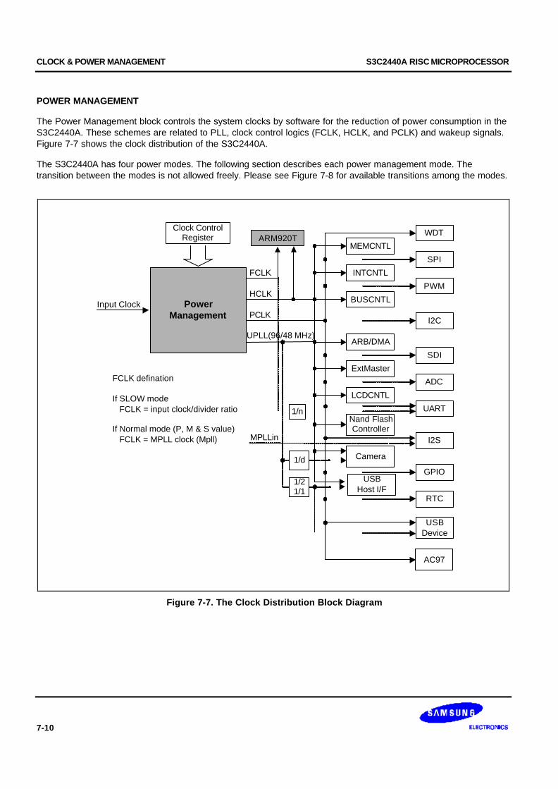
CLOCK & POWER MANAGEMENT S3C2440A RISC MICROPROCESSOR
7-10
POWER MANAGEMENT
The Power Management block controls the system clocks by software for the reduction of power consumption in theS3C2440A. These schemes are related to PLL, clock control logics (FCLK, HCLK, and PCLK) and wakeup signals.Figure 7-7 shows the clock distribution of the S3C2440A.
The S3C2440A has four power modes. The following section describes each power management mode. Thetransition between the modes is not allowed freely. Please see Figure 7-8 for available transitions among the modes.
INTCNTL
PowerManagement
FCLK
Input Clock
FCLK defination
If SLOW mode FCLK = input clock/divider ratio
If Normal mode (P, M & S value) FCLK = MPLL clock (Mpll)
ARM920T
HCLK
PCLK
UPLL(96/48 MHz)
BUSCNTL
MEMCNTL
ARB/DMA
ExtMaster
LCDCNTL
Nand FlashController
Camera
WDT
SPI
PWM
I2C
SDI
ADC
UART
I2S
GPIO
RTC
USBDevice
Clock ControlRegister
USBHost I/F
1/d
1/21/1
AC97
1/n
MPLLin
Figure 7-7. The Clock Distribution Block Diagram
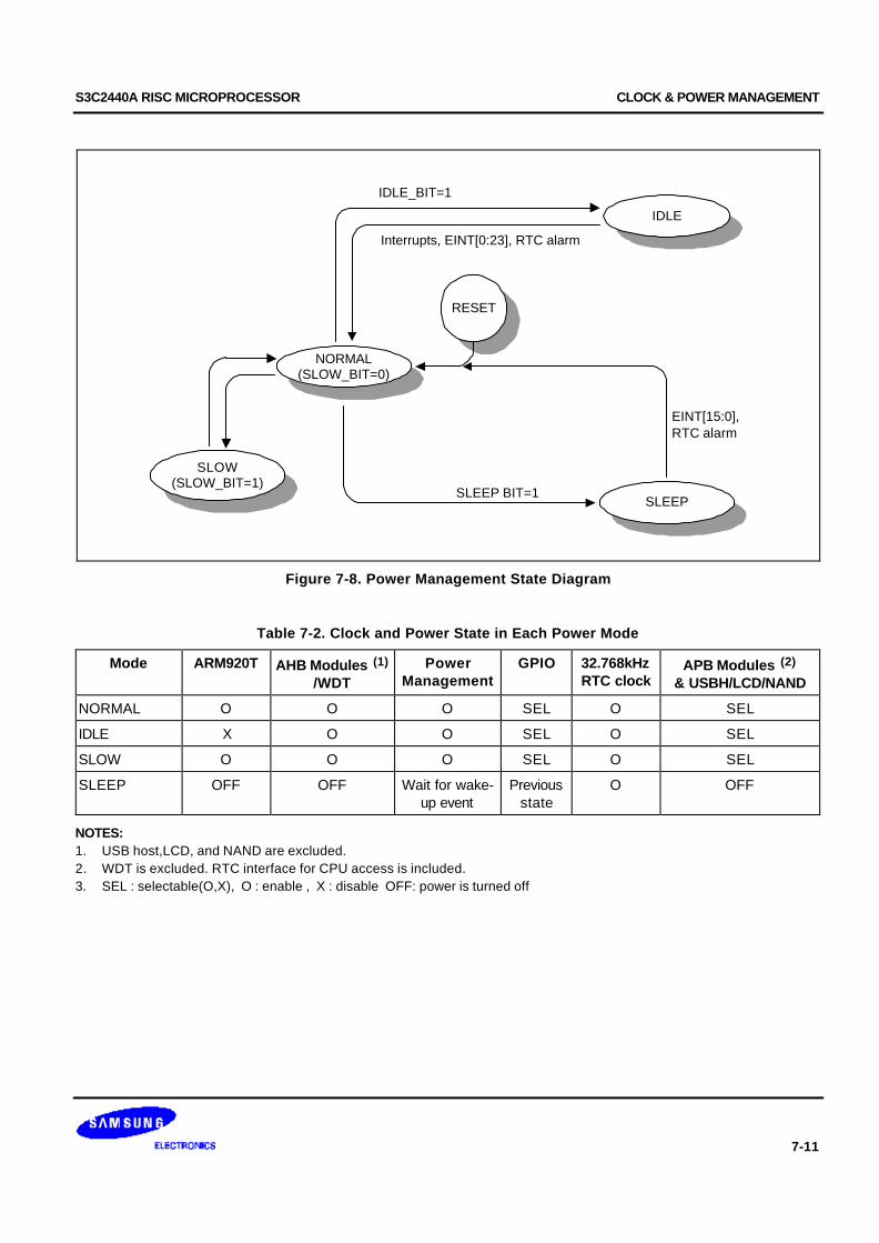
S3C2440A RISC MICROPROCESSOR CLOCK & POWER MANAGEMENT
7-11
IDLE
SLEEP
NORMAL(SLOW_BIT=0)
SLOW(SLOW_BIT=1)
IDLE_BIT=1
Interrupts, EINT[0:23], RTC alarm
SLEEP BIT=1
EINT[15:0],RTC alarm
RESET
Figure 7-8. Power Management State Diagram
Table 7-2. Clock and Power State in Each Power Mode
Mode ARM920T AHB Modules (1)
/WDTPower
ManagementGPIO 32.768kHz
RTC clockAPB Modules (2)
& USBH/LCD/NAND
NORMAL O O O SEL O SEL
IDLE X O O SEL O SEL
SLOW O O O SEL O SEL
SLEEP OFF OFF Wait for wake-up event
Previousstate
O OFF
NOTES:1. USB host,LCD, and NAND are excluded.2. WDT is excluded. RTC interface for CPU access is included.3. SEL : selectable(O,X), O : enable , X : disable OFF: power is turned off

CLOCK & POWER MANAGEMENT S3C2440A RISC MICROPROCESSOR
7-12
NORMAL Mode
In Normal mode, all peripherals and the basic blocks including power management block, the CPU core, the buscontroller, the memory controller, the interrupt controller, DMA, and the external master may operate completely.But, the clock to each peripheral, except the basic blocks, can be stopped selectively by software to reduce thepower consumption.
IDLE Mode
In IDLE mode, the clock to the CPU core is stopped except the bus controller, the memory controller, the interruptcontroller, and the power management block. To exit the IDLE mode, EINT[23:0], or RTC alarm interrupt, or the otherinterrupts should be activated. (EINT is not available until GPIO block is turned on).
SLOW Mode (Non-PLL Mode)
Power consumption can be reduced in the SLOW mode by applying a slow clock and excluding the powerconsumption from the PLL. The FCLK is the frequency of divide_by_n of the input clock (XTIpll or EXTCLK) withoutPLL. The divider ratio is determined by SLOW_VAL in the CLKSLOW control register and CLKDIVN control register.
Table 7-3. CLKSLOW and CLKDIVN Register Settings for SLOW Clock example
SLOW_VAL FCLK HCLK PCLK UCLK
1/1 Option(HDIVN=0)
1/2 Option(HDIVN=1)
1/1 Option(PDIVN=0)
1/2 Option(PDIVN=1)
0 0 0 EXTCLK orXTIpll / 1
EXTCLK orXTIpll / 1
EXTCLK orXTIpll / 2
HCLK HCLK / 2 48 MHz
0 0 1 EXTCLK orXTIpll / 2
EXTCLK orXTIpll / 2
EXTCLK orXTIpll / 4
HCLK HCLK / 2 48 MHz
0 1 0 EXTCLK orXTIpll / 4
EXTCLK orXTIpll / 4
EXTCLK orXTIpll / 8
HCLK HCLK / 2 48 MHz
0 1 1 EXTCLK orXTIpll / 6
EXTCLK orXTIpll / 6
EXTCLK orXTIpll / 12
HCLK HCLK / 2 48 MHz
1 0 0 EXTCLK orXTIpll / 8
EXTCLK orXTIpll / 8
EXTCLK orXTIpll / 16
HCLK HCLK / 2 48 MHz
1 0 1 EXTCLK orXTIpll / 10
EXTCLK orXTIpll / 10
EXTCLK orXTIpll / 20
HCLK HCLK / 2 48 MHz
1 1 0 EXTCLK orXTIpll / 12
EXTCLK orXTIpll / 12
EXTCLK orXTIpll / 24
HCLK HCLK / 2 48 MHz
1 1 1 EXTCLK orXTIpll / 14
EXTCLK orXTIpll / 14
EXTCLK orXTIpll / 28
HCLK HCLK / 2 48 MHz
In SLOW mode, PLL will be turned off to reduce the PLL power consumption. When the PLL is turned off in theSLOW mode and the user changes power mode from SLOW mode to NORMAL mode, then the PLL needs clockstabilization time (PLL lock time). This PLL stabilization time is automatically inserted by the internal logic with locktime count register. The PLL stability time will take 300us after the PLL is turned on. During PLL lock time, the FCLKbecomes SLOW clock.
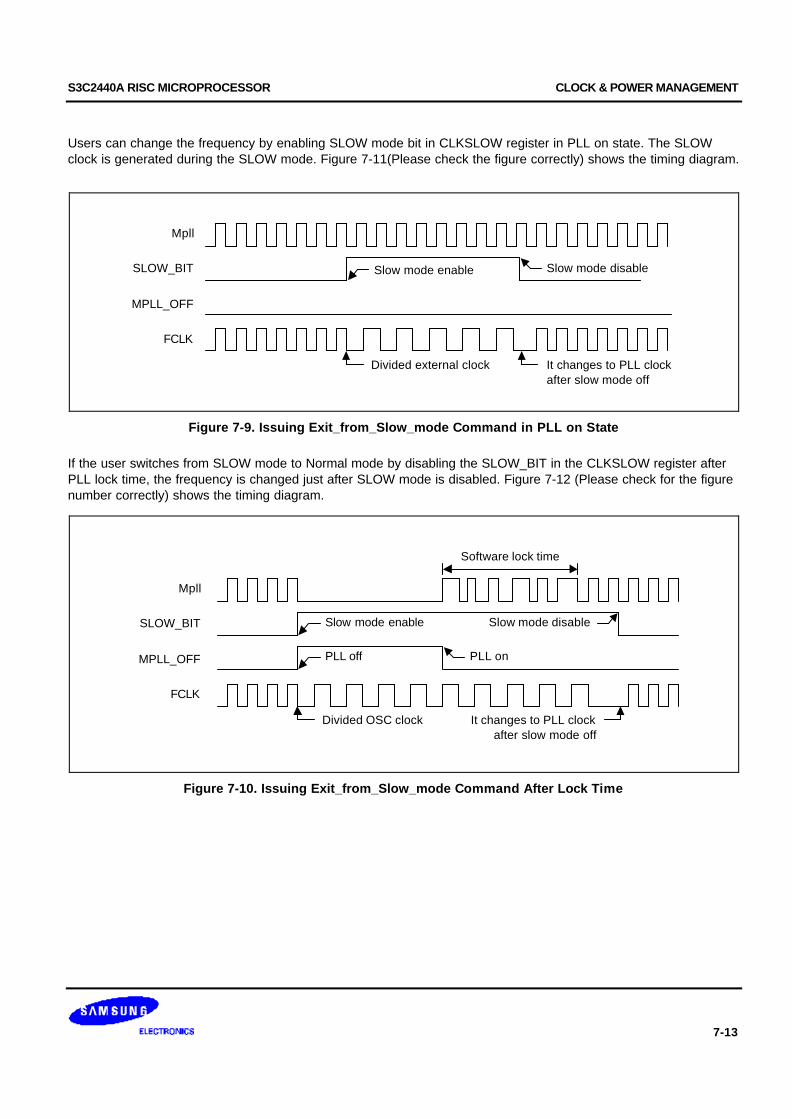
S3C2440A RISC MICROPROCESSOR CLOCK & POWER MANAGEMENT
7-13
Users can change the frequency by enabling SLOW mode bit in CLKSLOW register in PLL on state. The SLOWclock is generated during the SLOW mode. Figure 7-11(Please check the figure correctly) shows the timing diagram.
Mpll
Slow mode disable
FCLK
Slow mode enableSLOW_BIT
Divided external clock
MPLL_OFF
It changes to PLL clockafter slow mode off
Figure 7-9. Issuing Exit_from_Slow_mode Command in PLL on State
If the user switches from SLOW mode to Normal mode by disabling the SLOW_BIT in the CLKSLOW register afterPLL lock time, the frequency is changed just after SLOW mode is disabled. Figure 7-12 (Please check for the figurenumber correctly) shows the timing diagram.
Mpll
FCLK
SLOW_BIT
Divided OSC clock
MPLL_OFF
Software lock time
Slow mode disable
PLL off PLL on
Slow mode enable
It changes to PLL clockafter slow mode off
Figure 7-10. Issuing Exit_from_Slow_mode Command After Lock Time
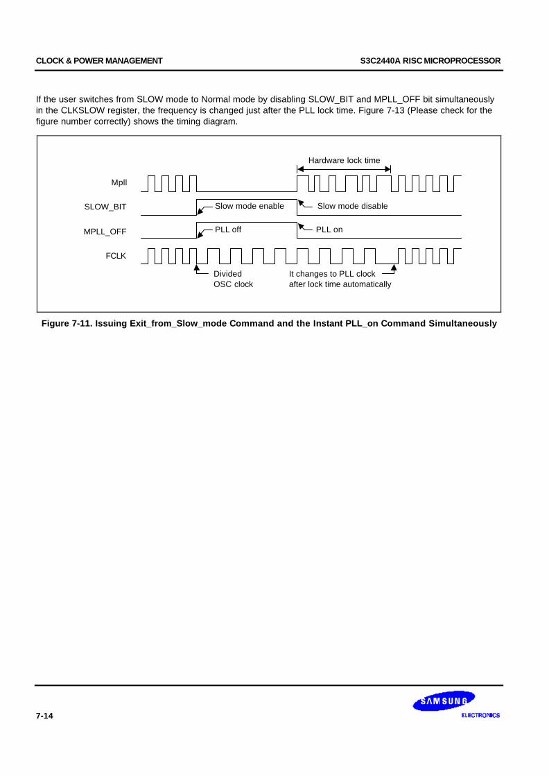
CLOCK & POWER MANAGEMENT S3C2440A RISC MICROPROCESSOR
7-14
If the user switches from SLOW mode to Normal mode by disabling SLOW_BIT and MPLL_OFF bit simultaneouslyin the CLKSLOW register, the frequency is changed just after the PLL lock time. Figure 7-13 (Please check for thefigure number correctly) shows the timing diagram.
Mpll
FCLK
SLOW_BIT
DividedOSC clock
MPLL_OFF
Hardware lock time
PLL off PLL on
Slow mode enable
It changes to PLL clockafter lock time automatically
Slow mode disable
Figure 7-11. Issuing Exit_from_Slow_mode Command and the Instant PLL_on Command Simultaneously

S3C2440A RISC MICROPROCESSOR CLOCK & POWER MANAGEMENT
7-15
SLEEP Mode
The block disconnects the internal power. So, there occurs no power consumption due to CPU and the internal logicexcept the wake-up logic in this mode. Activating the SLEEP mode requires two independent power sources. One ofthe two power sources supplies the power for the wake-up logic. The other one supplies other internal logicsincluding CPU, and should be controlled for power on/off. In the SLEEP mode, the second power supply source forthe CPU and internal logics will be turned off. The wakeup from SLEEP mode can be issued by the EINT[15:0] or byRTC alarm interrupt.
Follow the Procedure to Enter SLEEP mode
1. Set the GPIO configuration adequate for SLEEP mode.
2. Mask all interrupts in the INTMSK register.
3. Configure the wake-up sources properly including RTC alarm. (The bit of EINTMASK corresponding to the wake-up source has not to be masked in order to let the corresponding bit of SRCPND or EINTPEND set. Although awake-up source is issued and the corresponding bit of EINTMASK is masked, the wake-up will occur and thecorresponding bit of SRCPND or EINTPEND will not be set.)
4. Set USB pads as suspend mode. (MISCCR[13:12]=11b)
5. Save some meaning values into GSTATUS[4:3] register. These register are preserved during SLEEP mode.
6. Configure MISCCR[1:0] for the pull-up resisters on the data bus,D[31:0]. If there is an external BUS holder, suchas 74LVCH162245, turn off the pull-up resistors. If not, turn on the pull-up resistors.Additionally, The Memory concerning pins is set to two types, one is Hi-z, and the other is Inactive state.
7. Stop LCD by clearing LCDCON1.ENVID bit.
8. Read rREFRESH and rCLKCON registers in order to fill the TLB.
9. Let SDRAM enter the self-refresh mode by setting the REFRESH[22]=1b.
10. Wait until SDRAM self-refresh is effective.
11. Set MISCCR[19:17]=111b to make SDRAM signals(SCLK0,SCLK1 and SCKE) protected during SLEEP mode
12. Set the SLEEP mode bit in the CLKCON register.
Caution: When the system is operating in NAND boot mode, The hardware pin configuration - EINT[23:21] – must be set as input for starting up after wakeup from sleep mode.

CLOCK & POWER MANAGEMENT S3C2440A RISC MICROPROCESSOR
7-16
Follow the Procedure to Wake-up from SLEEP mode
1. The internal reset signal will be asserted if one of the wake-up sources is issued. It’s exactly same with the caseof the assertion of the external nRESET pin. This reset duration is determined by the internal 16-bit counter logicand the reset assertion time is calculated as tRST = (65535 / XTAL_frequency).
2. Check GSTATUS2[2] in order to know whether or not the power-up is caused by the wake-up from SLEEPmode.
3. Release the SDRAM signal protection by setting MISCCR[19:17]=000b.
4. Configure the SDRAM memory controller.
5. Wait until the SDRAM self-refresh is released. Mostly SDRAM needs the refresh cycle of all SDRAM row.
6. The information in GSTATUS[3:4] can be used for user’s own purpose because the value in GSTATUS[3:4] hasbeen preserved during SLEEP mode.
7. – For EINT[3:0], check the SRCPND register.– For EINT[15:4], check the EINTPEND instead of SRCPND (SRCPND will not be set although some bits of EINTPEND are set.).
Table 7-4. Pin configuration table in Sleep mode
Pin Condition Guid of Pin Configuration
GPIO Pin which are configured as input Pull-up enable
which are configured as ouput Pull-up disable and output low
Input pin, which doesn't haveinternal pull-up control.
If external device doesn't alwaysdrive pin's level.
Pull-up enable by external pull-up resistor
Output pin, which areconnected to external device
If external device's power is off Output low
If external device's power is on High or low(It depends on External device's status)
DataBus
If memory power is off Output low
If memory power is on and external buffer does exist If buffer can hold bus level, pull-up disable.
and no external buffer Output low
NOTE:1. ADC should be set to Standby mode.2. USB pads should be Suspend mode.
* This table is just for informational use only. User should consider his own board condition and application.
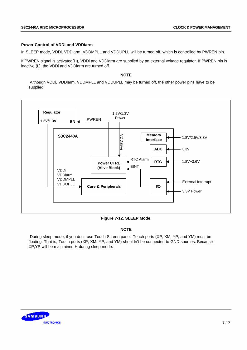
S3C2440A RISC MICROPROCESSOR CLOCK & POWER MANAGEMENT
7-17
Power Control of VDDi and VDDiarm
In SLEEP mode, VDDi, VDDiarm, VDDMPLL and VDDUPLL will be turned off, which is controlled by PWREN pin.
If PWREN signal is activated(H), VDDi and VDDiarm are supplied by an external voltage regulator. If PWREN pin isinactive (L), the VDDi and VDDiarm are turned off.
NOTE
Although VDDi, VDDiarm, VDDMPLL and VDDUPLL may be turned off, the other power pins have to besupplied.
S3C2440A
Power CTRL(Alive Block)
RTC Alarm
EINT
External Interrupt
3.3V Power
PWREN
VDDiVDDiarmVDDMPLLVDDUPLL
Core & Peripherals
RTC
I/O
Regulator
1.2V/1.3V EN
1.2V/1.3VPower
VD
Dalive ADC
1.8V~3.6V
MemoryInterface 1.8V/2.5V/3.3V
3.3V
Figure 7-12. SLEEP Mode
NOTE
During sleep mode, if you don’t use Touch Screen panel, Touch ports (XP, XM, YP, and YM) must befloating. That is, Touch ports (XP, XM, YP, and YM) shouldn’t be connected to GND sources. BecauseXP,YP will be maintained H during sleep mode.
CLOCK & POWER MANAGEMENT S3C2440A RISC MICROPROCESSOR
7-18
Signaling EINT[15:0] for Wakeup
The S3C2440A can be woken up from SLEEP mode only if the following conditions are met.
a) Level signals (H or L) or edge signals (rising, falling or both) are asserted on EINTn input pin.
b) The EINTn pin has to be configured as EINT in the GPIO control register.
c) nBATT_FLT pin has to be H level. It is important to configure the EINTn in the GPIO control register as anexternal interrupt pins, considering the condition a) above.
Just after the wake-up, the corresponding EINTn pin will not be used for wakeup. This means that the pin can beused as an external interrupt request pin again.
Entering IDLE Mode
If CLKCON[2] is set to 1 to enter the IDLE mode, the S3C2440A will enter IDLE mode after some delay (until thepower control logic receives ACK signal from the CPU wrapper).
PLL On/Off
The PLL can only be turned off for low power consumption in slow mode. If the PLL is turned off in any other mode,MCU operation is not guaranteed.
When the processor is in SLOW mode and tries to change its state into other state with the PLL turned on, thenSLOW_BIT should be clear to move to another state after PLL stabilization
Pull-up Resistors on the Data Bus and SLEEP Mode
In SLEEP mode, the data bus (D[31:0] or D[15:0] ) can be selected as Hi-z state and Output Low state.
The data bus can be set as Hi-z status with turning on pull-up register or can be set as output low with turning offpull-up register for low power consumption in SLEEP mode. D[31:0] pin pull-up resistors can be controlled by theGPIO control register (MISCCR). However, if there is an external bus holder, such as 74LVCH162245, on the databus, User can select one of two status – one is output low with pull-up off, the other is Hi-z with pull-up off - , whichconsumes less power.
S3C2440A RISC MICROPROCESSOR CLOCK & POWER MANAGEMENT
7-19
Output Port State and SLEEP Mode
The output port should have a proper logic level in power off mode, which makes the current consumption minimized.If there is no load on an output port pin, H level is preferred. If output is L, the current will be consumed through theinternal parasitic resistance; if the output is H, the current will not be consumed. For an output port, the currentconsumption can be reduced if the output state is H.
It is recommended that the output ports be in H state to reduce current consumption in SLEEP mode.
Battery Fault Signal (nBATT_FLT)
There are two functions in nBATT_FLT pin, they are as follows;
— When CPU is not in SLEEP mode, nBATT_FLT pin will cause the interrupt request by settingBATT_FUNC(MISCCR[22:20]) as 10x’b. The interrupt attribute of the nBATT_FLT is L-level triggered.
— While CPU is in SLEEP mode, assertion of the nBATT_FLT will prohibit the wake up from the sleep mode, whichis achieved by setting BATT_FUNC(MISCCR[22:20]) as 11x’b. So, Any wake-up source will be masked ifnBATT_FLT is asserted, which is protecting the system malfunction of the low battery capacity
ADC Power Down
The ADC has an additional power-down bit in ADCCON. If the S3C2440A enters the SLEEP mode, the ADC shouldenter its own power-down mode.
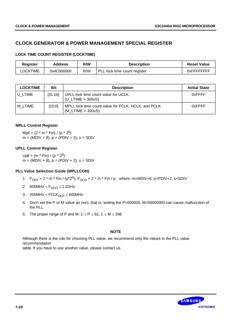
CLOCK & POWER MANAGEMENT S3C2440A RISC MICROPROCESSOR
7-20
CLOCK GENERATOR & POWER MANAGEMENT SPECIAL REGISTER
LOCK TIME COUNT REGISTER (LOCKTIME)
Register Address R/W Description Reset Value
LOCKTIME 0x4C000000 R/W PLL lock time count register 0xFFFFFFFF
LOCKTIME Bit Description Initial State
U_LTIME [31:16] UPLL lock time count value for UCLK.(U_LTIME > 300uS)
0xFFFF
M_LTIME [15:0] MPLL lock time count value for FCLK, HCLK, and PCLK(M_LTIME > 300uS)
0xFFFF
MPLL Control Register
Mpll = (2 * m * Fin) / (p * 2S)m = (MDIV + 8), p = (PDIV + 2), s = SDIV
UPLL Control Register
Upll = (m * Fin) / (p * 2S)m = (MDIV + 8), p = (PDIV + 2), s = SDIV
PLL Value Selection Guide (MPLLCON)
1. FOUT = 2 * m * Fin / (p*2S), FVCO = 2 * m * Fin / p where: m=MDIV+8, p=PDIV+2, s=SDIV
2. 600MHz ≤ FVCO ≤ 1.2GHz
3. 200MHz ≤ FCLKOUT ≤ 600MHz
4. Don't set the P or M value as zero, that is, setting the P=000000, M=00000000 can cause malfunction of the PLL.
5. The proper range of P and M: 1 ≤ P ≤ 62, 1 ≤ M ≤ 248
NOTE
Although there is the rule for choosing PLL value, we recommend only the values in the PLL valuerecommendationtable. If you have to use another value, please contact us.
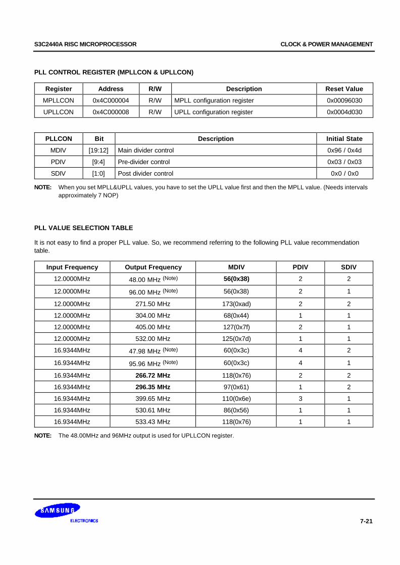
S3C2440A RISC MICROPROCESSOR CLOCK & POWER MANAGEMENT
7-21
PLL CONTROL REGISTER (MPLLCON & UPLLCON)
Register Address R/W Description Reset Value
MPLLCON 0x4C000004 R/W MPLL configuration register 0x00096030
UPLLCON 0x4C000008 R/W UPLL configuration register 0x0004d030
PLLCON Bit Description Initial State
MDIV [19:12] Main divider control 0x96 / 0x4d
PDIV [9:4] Pre-divider control 0x03 / 0x03
SDIV [1:0] Post divider control 0x0 / 0x0
NOTE: When you set MPLL&UPLL values, you have to set the UPLL value first and then the MPLL value. (Needs intervals approximately 7 NOP)
PLL VALUE SELECTION TABLE
It is not easy to find a proper PLL value. So, we recommend referring to the following PLL value recommendationtable.
Input Frequency Output Frequency MDIV PDIV SDIV
12.0000MHz 48.00 MHz (Note) 56(0x38) 2 2
12.0000MHz 96.00 MHz (Note) 56(0x38) 2 1
12.0000MHz 271.50 MHz 173(0xad) 2 2
12.0000MHz 304.00 MHz 68(0x44) 1 1
12.0000MHz 405.00 MHz 127(0x7f) 2 1
12.0000MHz 532.00 MHz 125(0x7d) 1 1
16.9344MHz 47.98 MHz (Note) 60(0x3c) 4 2
16.9344MHz 95.96 MHz (Note) 60(0x3c) 4 1
16.9344MHz 266.72 MHz 118(0x76) 2 2
16.9344MHz 296.35 MHz 97(0x61) 1 2
16.9344MHz 399.65 MHz 110(0x6e) 3 1
16.9344MHz 530.61 MHz 86(0x56) 1 1
16.9344MHz 533.43 MHz 118(0x76) 1 1
NOTE: The 48.00MHz and 96MHz output is used for UPLLCON register.
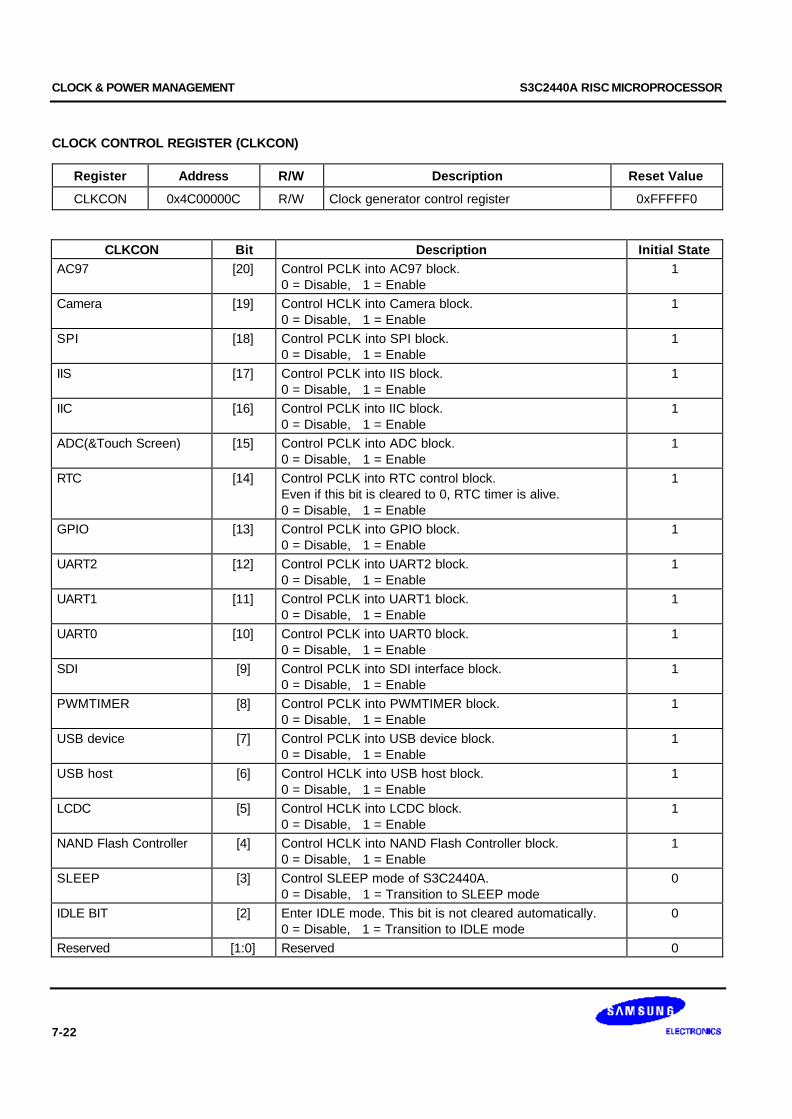
CLOCK & POWER MANAGEMENT S3C2440A RISC MICROPROCESSOR
7-22
CLOCK CONTROL REGISTER (CLKCON)
Register Address R/W Description Reset Value
CLKCON 0x4C00000C R/W Clock generator control register 0xFFFFF0
CLKCON Bit Description Initial StateAC97 [20] Control PCLK into AC97 block.
0 = Disable, 1 = Enable1
Camera [19] Control HCLK into Camera block.0 = Disable, 1 = Enable
1
SPI [18] Control PCLK into SPI block.0 = Disable, 1 = Enable
1
IIS [17] Control PCLK into IIS block.0 = Disable, 1 = Enable
1
IIC [16] Control PCLK into IIC block.0 = Disable, 1 = Enable
1
ADC(&Touch Screen) [15] Control PCLK into ADC block.0 = Disable, 1 = Enable
1
RTC [14] Control PCLK into RTC control block.Even if this bit is cleared to 0, RTC timer is alive.0 = Disable, 1 = Enable
1
GPIO [13] Control PCLK into GPIO block.0 = Disable, 1 = Enable
1
UART2 [12] Control PCLK into UART2 block.0 = Disable, 1 = Enable
1
UART1 [11] Control PCLK into UART1 block.0 = Disable, 1 = Enable
1
UART0 [10] Control PCLK into UART0 block.0 = Disable, 1 = Enable
1
SDI [9] Control PCLK into SDI interface block.0 = Disable, 1 = Enable
1
PWMTIMER [8] Control PCLK into PWMTIMER block.0 = Disable, 1 = Enable
1
USB device [7] Control PCLK into USB device block.0 = Disable, 1 = Enable
1
USB host [6] Control HCLK into USB host block.0 = Disable, 1 = Enable
1
LCDC [5] Control HCLK into LCDC block.0 = Disable, 1 = Enable
1
NAND Flash Controller [4] Control HCLK into NAND Flash Controller block.0 = Disable, 1 = Enable
1
SLEEP [3] Control SLEEP mode of S3C2440A.0 = Disable, 1 = Transition to SLEEP mode
0
IDLE BIT [2] Enter IDLE mode. This bit is not cleared automatically.0 = Disable, 1 = Transition to IDLE mode
0
Reserved [1:0] Reserved 0

S3C2440A RISC MICROPROCESSOR CLOCK & POWER MANAGEMENT
7-23
CLOCK SLOW CONTROL (CLKSLOW) REGISTER
Register Address R/W Description Reset Value
CLKSLOW 0x4C000010 R/W Slow clock control register 0x00000004
CLKSLOW Bit Description Initial State
UCLK_ON [7] 0: UCLK ON (UPLL is also turned on and the UPLL lock time isinserted automatically.)
1: UCLK OFF (UPLL is also turned off.)
0
Reserved [6] Reserved –
MPLL_OFF [5] 0: Turn on PLL. After PLL stabilization time (minimum 300us), SLOW_BIT can be cleared to 0.
1: Turn off PLL. PLL is turned off only when SLOW_BIT is 1.
0
SLOW_BIT [4] 0 : FCLK = Mpll (MPLL output)1: SLOW mode
FCLK = input clock/(2xSLOW_VAL), when SLOW_VAL>0FCLK = input clock, when SLOW_VAL=0.
Input clock = XTIpll or EXTCLK
0
Reserved [3] – –
SLOW_VAL [2:0] The divider value for the slow clock when SLOW_BIT is on. 0x4
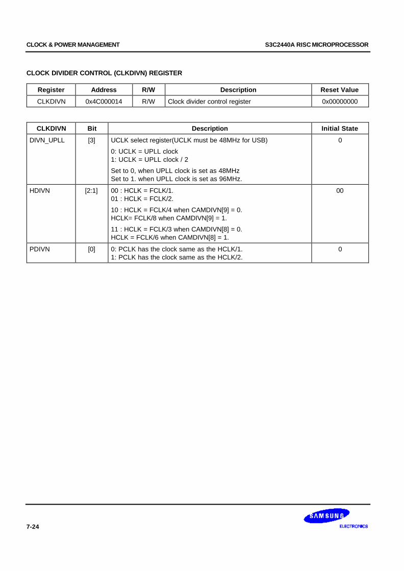
CLOCK & POWER MANAGEMENT S3C2440A RISC MICROPROCESSOR
7-24
CLOCK DIVIDER CONTROL (CLKDIVN) REGISTER
Register Address R/W Description Reset Value
CLKDIVN 0x4C000014 R/W Clock divider control register 0x00000000
CLKDIVN Bit Description Initial State
DIVN_UPLL [3] UCLK select register(UCLK must be 48MHz for USB)
0: UCLK = UPLL clock1: UCLK = UPLL clock / 2
Set to 0, when UPLL clock is set as 48MHzSet to 1. when UPLL clock is set as 96MHz.
0
HDIVN [2:1] 00 : HCLK = FCLK/1.01 : HCLK = FCLK/2.
10 : HCLK = FCLK/4 when CAMDIVN[9] = 0.HCLK= FCLK/8 when CAMDIVN[9] = 1.
11 : HCLK = FCLK/3 when CAMDIVN[8] = 0.HCLK = FCLK/6 when CAMDIVN[8] = 1.
00
PDIVN [0] 0: PCLK has the clock same as the HCLK/1.1: PCLK has the clock same as the HCLK/2.
0
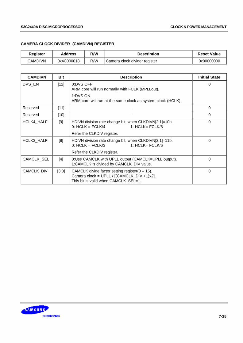
S3C2440A RISC MICROPROCESSOR CLOCK & POWER MANAGEMENT
7-25
CAMERA CLOCK DIVIDER (CAMDIVN) REGISTER
Register Address R/W Description Reset Value
CAMDIVN 0x4C000018 R/W Camera clock divider register 0x00000000
CAMDIVN Bit Description Initial State
DVS_EN [12] 0:DVS OFFARM core will run normally with FCLK (MPLLout).
1:DVS ONARM core will run at the same clock as system clock (HCLK).
0
Reserved [11] – 0
Reserved [10] – 0
HCLK4_HALF [9] HDIVN division rate change bit, when CLKDIVN[2:1]=10b.0: HCLK = FCLK/4 1: HCLK= FCLK/8
Refer the CLKDIV register.
0
HCLK3_HALF [8] HDIVN division rate change bit, when CLKDIVN[2:1]=11b.0: HCLK = FCLK/3 1: HCLK= FCLK/6
Refer the CLKDIV register.
0
CAMCLK_SEL [4] 0:Use CAMCLK with UPLL output (CAMCLK=UPLL output).1:CAMCLK is divided by CAMCLK_DIV value.
0
CAMCLK_DIV [3:0] CAMCLK divide factor setting register(0 – 15).Camera clock = UPLL / [(CAMCLK_DIV +1)x2].This bit is valid when CAMCLK_SEL=1.
0
S3C2440A RISC MICROPROCESSOR DMA
8-1
8 DMA
OVERVIEW
The S3C2440A supports four-channel DMA controller located between the system bus and the peripheral bus. Eachchannel of DMA controller can perform data movements between devices in the system bus and/or peripheral buswith no restrictions. In other words, each channel can handle the following four cases:
1. Both source and destination are in the system bus
2. The source is in the system bus while the destination is in the peripheral bus
3. The source is in the peripheral bus while the destination is in the system bus
4. Both source and destination are in the peripheral bus
The main advantage of the DMA is that it can transfer the data without CPU intervention. The operation of DMA canbe initiated by software, or requests from internal peripherals or external request pins.

DMA S3C2440A RISC MICROPROCESSOR
8-2
DMA REQUEST SOURCES
Each channel of the DMA controller can select one of the DMA request source among four DMA sources, if H/WDMA request mode is selected by DCON register. (Note that if S/W request mode is selected, this DMA requestsources have no meaning at all.) Table 8-1 shows four DMA sources for each channel.
Table 8-1. DMA Request Sources for Each Channel
Source0 Source1 Source2 Source3 Source4 Source5 Source6
Ch-0 nXDREQ0 UART0 SDI Timer USB device EP1 I2SSDO PCMIN
Ch-1 nXDREQ1 UART1 I2SSDI SPI0 USB device EP2 PCMOUT SDI
Ch-2 I2SSDO I2SSDI SDI Timer USB device EP3 PCMIN MICIN
Ch-3 UART2 SDI SPI1 Timer USB device EP4 MICIN PCMOUT
Here, nXDREQ0 and nXDREQ1 represent two external sources (External Devices), and I2SSDO and I2SSDIrepresent IIS transmitting and receiving, respectively.
DMA OPERATION
DMA uses three-state FSM (Finite State Machine) for its operation, which is described in the three following steps:
State-1. As an initial state, the DMA waits for a DMA request. Once the request is reached it goes to state-2. At this state, DMA ACK and INT REQ are 0.
State-2. In this state, DMA ACK becomes 1 and the counter (CURR_TC) is loaded from DCON[19:0] register. Note that the DMA ACK remains 1 until it is cleared later.
State-3. In this state, sub-FSM which handles the atomic operation of DMA is initiated. The sub-FSM reads the data from the source address and then writes it to destination address. In this operation, data size and transfer size (single or burst) are considered. This operation is repeated until the counter
(CURR_TC) becomes 0 in Whole service mode, while performed only once in Single service mode. The main FSM (this FSM) counts down the CURR_TC when the sub-FSM finishes each of atomic operation. In addition, this main FSM asserts the INT REQ signal when CURR_TC becomes 0 and the interrupt setting of DCON[29] register is set to 1. In addition, it clears DMA ACK .if one of the following conditions is met.
1) CURR_TC becomes 0 in the Whole service mode2) Atomic operation finishes in the Single service mode.
Note that in the Single service mode, these three states of main FSM are performed and then stops, and wait foranother DMA REQ. And if DMA REQ comes in, all three states are repeated. Therefore, DMA ACK is asserted andthen de-asserted for each atomic transfer. In contrast, in the Whole service mode, main FSM waits at state-3 untilCURR_TC becomes 0. Therefore, DMA ACK is asserted during all the transfers and then de-asserted when TCreaches 0.
However, INT REQ is asserted only if CURR_TC becomes 0 regardless of the service mode (Single service mode orWhole service mode).
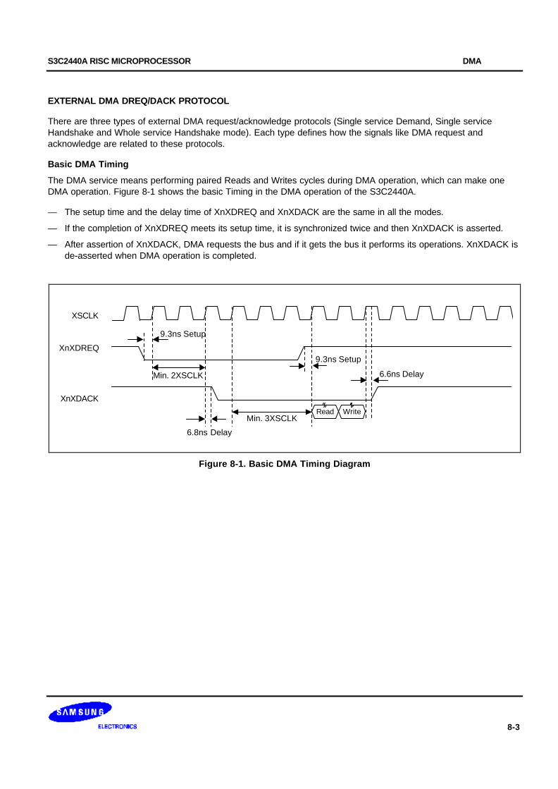
S3C2440A RISC MICROPROCESSOR DMA
8-3
EXTERNAL DMA DREQ/DACK PROTOCOL
There are three types of external DMA request/acknowledge protocols (Single service Demand, Single serviceHandshake and Whole service Handshake mode). Each type defines how the signals like DMA request andacknowledge are related to these protocols.
Basic DMA Timing
The DMA service means performing paired Reads and Writes cycles during DMA operation, which can make oneDMA operation. Figure 8-1 shows the basic Timing in the DMA operation of the S3C2440A.
— The setup time and the delay time of XnXDREQ and XnXDACK are the same in all the modes.
— If the completion of XnXDREQ meets its setup time, it is synchronized twice and then XnXDACK is asserted.
— After assertion of XnXDACK, DMA requests the bus and if it gets the bus it performs its operations. XnXDACK isde-asserted when DMA operation is completed.
XSCLK
9.3ns Setup
9.3ns Setup
6.8ns Delay
6.6ns Delay
Read Write
Min. 2XSCLK
XnXDREQ
XnXDACK
Min. 3XSCLK
Figure 8-1. Basic DMA Timing Diagram
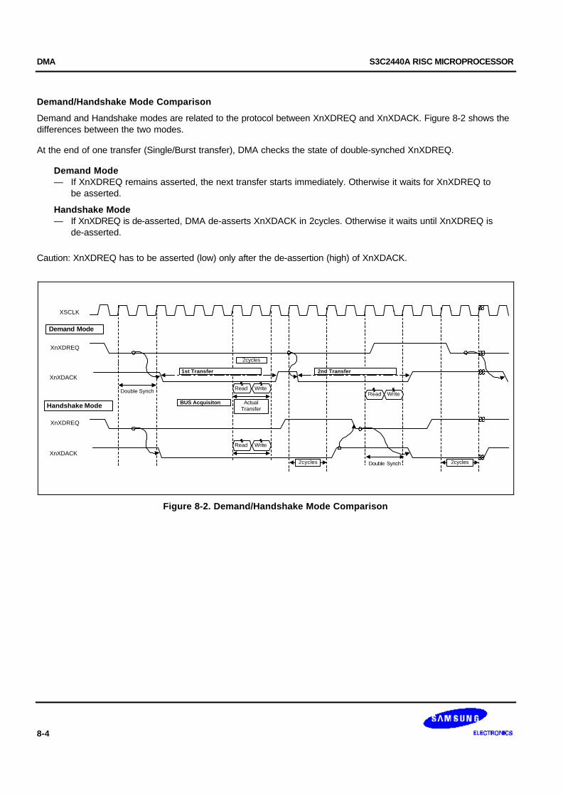
DMA S3C2440A RISC MICROPROCESSOR
8-4
Demand/Handshake Mode Comparison
Demand and Handshake modes are related to the protocol between XnXDREQ and XnXDACK. Figure 8-2 shows thedifferences between the two modes.
At the end of one transfer (Single/Burst transfer), DMA checks the state of double-synched XnXDREQ.
Demand Mode— If XnXDREQ remains asserted, the next transfer starts immediately. Otherwise it waits for XnXDREQ to be asserted.
Handshake Mode— If XnXDREQ is de-asserted, DMA de-asserts XnXDACK in 2cycles. Otherwise it waits until XnXDREQ is de-asserted.
Caution: XnXDREQ has to be asserted (low) only after the de-assertion (high) of XnXDACK.
Demand Mode
XSCLK
XnXDACK
XnXDACK
XnXDREQ
XnXDREQ
2cycles
Double Synch Read WriteRead Write
Handshake Mode BUS Acquisiton ActualTransfer
1st Transfer 2nd Transfer
2cycles
Read Write
Double Synch 2cycles
Figure 8-2. Demand/Handshake Mode Comparison
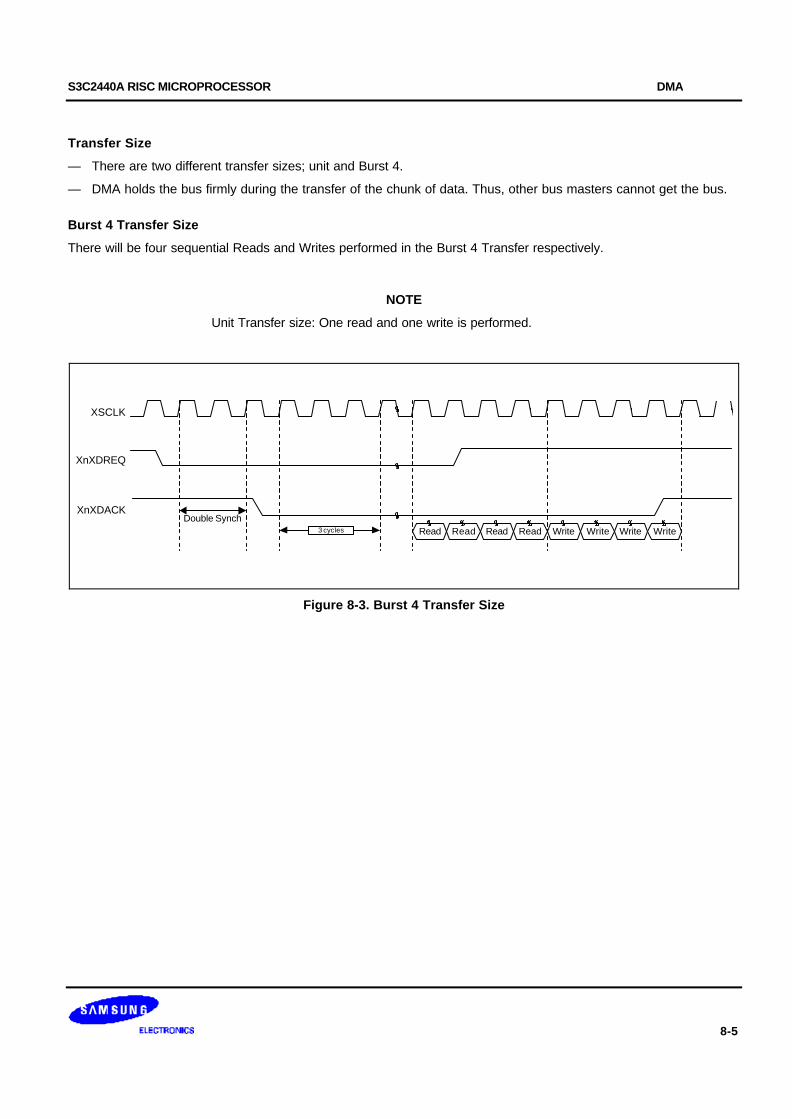
S3C2440A RISC MICROPROCESSOR DMA
8-5
Transfer Size
— There are two different transfer sizes; unit and Burst 4.
— DMA holds the bus firmly during the transfer of the chunk of data. Thus, other bus masters cannot get the bus.
Burst 4 Transfer Size
There will be four sequential Reads and Writes performed in the Burst 4 Transfer respectively.
NOTE
Unit Transfer size: One read and one write is performed.
XSCLK
XnXDREQ
XnXDACK
Read Read Read Write Write WriteRead Write3 cycles
Double Synch
Figure 8-3. Burst 4 Transfer Size
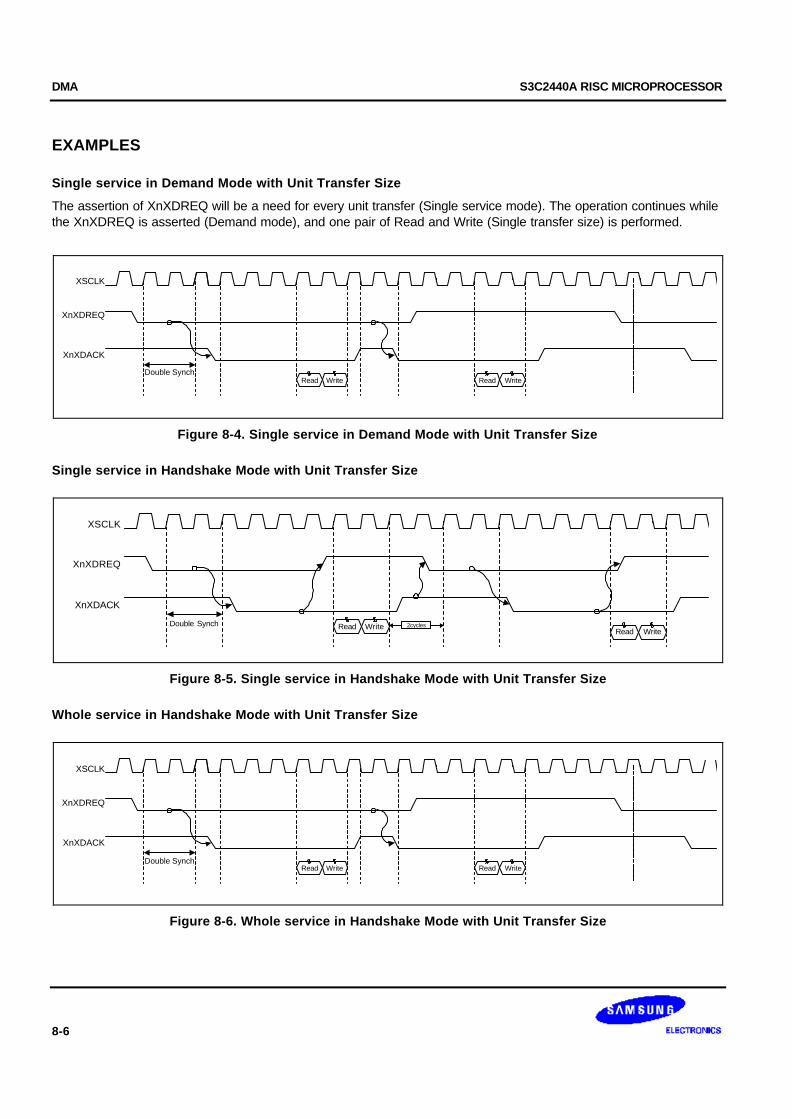
DMA S3C2440A RISC MICROPROCESSOR
8-6
EXAMPLES
Single service in Demand Mode with Unit Transfer Size
The assertion of XnXDREQ will be a need for every unit transfer (Single service mode). The operation continues whilethe XnXDREQ is asserted (Demand mode), and one pair of Read and Write (Single transfer size) is performed.
XnXDREQ
XnXDACK
XSCLK
Read Write Read WriteDouble Synch
Figure 8-4. Single service in Demand Mode with Unit Transfer Size
Single service in Handshake Mode with Unit Transfer Size
XnXDREQ
XnXDACK
XSCLK
Read WriteRead Write
2cyclesDouble Synch
Figure 8-5. Single service in Handshake Mode with Unit Transfer Size
Whole service in Handshake Mode with Unit Transfer Size
XnXDREQ
XnXDACK
XSCLK
Read Write Read WriteDouble Synch
Figure 8-6. Whole service in Handshake Mode with Unit Transfer Size

S3C2440A RISC MICROPROCESSOR DMA
8-7
DMA SPECIAL REGISTERS
Each DMA channel has nine control registers (36 in total since there are four channels for DMA controller). Six of thecontrol registers control the DMA transfer, and other three ones monitor the status of DMA controller. The details ofthose registers are as follows.
DMA INITIAL SOURCE (DISRC) REGISTER
Register Address R/W Description Reset Value
DISRC0 0x4B000000 R/W DMA 0 initial source register 0x00000000
DISRC1 0x4B000040 R/W DMA 1 initial source register 0x00000000
DISRC2 0x4B000080 R/W DMA 2 initial source register 0x00000000
DISRC3 0x4B0000C0 R/W DMA 3 initial source register 0x00000000
DISRCn Bit Description Initial State
S_ADDR [30:0] Base address (start address) of source data to transfer. This bitvalue will be loaded into CURR_SRC only if the CURR_SRC is 0and the DMA ACK is 1.
0x00000000
DMA INITIAL SOURCE CONTROL (DISRCC) REGISTER
Register Address R/W Description Reset Value
DISRCC0 0x4B000004 R/W DMA 0 initial source control register 0x00000000
DISRCC1 0x4B000044 R/W DMA 1 initial source control register 0x00000000
DISRCC2 0x4B000084 R/W DMA 2 initial source control register 0x00000000
DISRCC3 0x4B0000C4 R/W DMA 3 initial source control register 0x00000000
DISRCCn Bit Description Initial State
LOC [1] Bit 1 is used to select the location of source.0: the source is in the system bus (AHB).1: the source is in the peripheral bus (APB).
0
INC [0] Bit 0 is used to select the address increment.0 = Increment 1= Fixed
If it is 0, the address is increased by its data size after eachtransfer in burst and single transfer mode.
If it is 1, the address is not changed after the transfer. (In the burstmode, address is increased during the burst transfer, but theaddress is recovered to its first value after the transfer.)
0
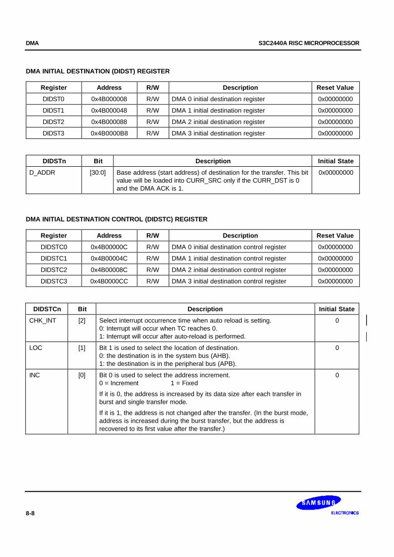
DMA S3C2440A RISC MICROPROCESSOR
8-8
DMA INITIAL DESTINATION (DIDST) REGISTER
Register Address R/W Description Reset Value
DIDST0 0x4B000008 R/W DMA 0 initial destination register 0x00000000
DIDST1 0x4B000048 R/W DMA 1 initial destination register 0x00000000
DIDST2 0x4B000088 R/W DMA 2 initial destination register 0x00000000
DIDST3 0x4B0000B8 R/W DMA 3 initial destination register 0x00000000
DIDSTn Bit Description Initial State
D_ADDR [30:0] Base address (start address) of destination for the transfer. This bitvalue will be loaded into CURR_SRC only if the CURR_DST is 0and the DMA ACK is 1.
0x00000000
DMA INITIAL DESTINATION CONTROL (DIDSTC) REGISTER
Register Address R/W Description Reset Value
DIDSTC0 0x4B00000C R/W DMA 0 initial destination control register 0x00000000
DIDSTC1 0x4B00004C R/W DMA 1 initial destination control register 0x00000000
DIDSTC2 0x4B00008C R/W DMA 2 initial destination control register 0x00000000
DIDSTC3 0x4B0000CC R/W DMA 3 initial destination control register 0x00000000
DIDSTCn Bit Description Initial State
CHK_INT [2] Select interrupt occurrence time when auto reload is setting.0: Interrupt will occur when TC reaches 0.1: Interrupt will occur after auto-reload is performed.
0
LOC [1] Bit 1 is used to select the location of destination.0: the destination is in the system bus (AHB).1: the destination is in the peripheral bus (APB).
0
INC [0] Bit 0 is used to select the address increment.0 = Increment 1 = Fixed
If it is 0, the address is increased by its data size after each transfer inburst and single transfer mode.
If it is 1, the address is not changed after the transfer. (In the burst mode,address is increased during the burst transfer, but the address isrecovered to its first value after the transfer.)
0
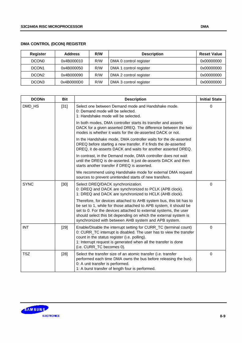
S3C2440A RISC MICROPROCESSOR DMA
8-9
DMA CONTROL (DCON) REGISTER
Register Address R/W Description Reset Value
DCON0 0x4B000010 R/W DMA 0 control register 0x00000000
DCON1 0x4B000050 R/W DMA 1 control register 0x00000000
DCON2 0x4B000090 R/W DMA 2 control register 0x00000000
DCON3 0x4B0000D0 R/W DMA 3 control register 0x00000000
DCONn Bit Description Initial State
DMD_HS [31] Select one between Demand mode and Handshake mode.0: Demand mode will be selected.1: Handshake mode will be selected.
In both modes, DMA controller starts its transfer and assertsDACK for a given asserted DREQ. The difference between the twomodes is whether it waits for the de-asserted DACK or not.
In the Handshake mode, DMA controller waits for the de-assertedDREQ before starting a new transfer. If it finds the de-assertedDREQ, it de-asserts DACK and waits for another asserted DREQ.
In contrast, in the Demand mode, DMA controller does not waituntil the DREQ is de-asserted. It just de-asserts DACK and thenstarts another transfer if DREQ is asserted.
We recommend using Handshake mode for external DMA requestsources to prevent unintended starts of new transfers.
0
SYNC [30] Select DREQ/DACK synchronization.0: DREQ and DACK are synchronized to PCLK (APB clock).1: DREQ and DACK are synchronized to HCLK (AHB clock).
Therefore, for devices attached to AHB system bus, this bit has tobe set to 1, while for those attached to APB system, it should beset to 0. For the devices attached to external systems, the usershould select this bit depending on which the external system issynchronized with between AHB system and APB system.
0
INT [29] Enable/Disable the interrupt setting for CURR_TC (terminal count)0: CURR_TC interrupt is disabled. The user has to view the transfercount in the status register (i.e. polling).1: Interrupt request is generated when all the transfer is done(i.e. CURR_TC becomes 0).
0
TSZ [28] Select the transfer size of an atomic transfer (i.e. transferperformed each time DMA owns the bus before releasing the bus).0: A unit transfer is performed.1: A burst transfer of length four is performed.
0
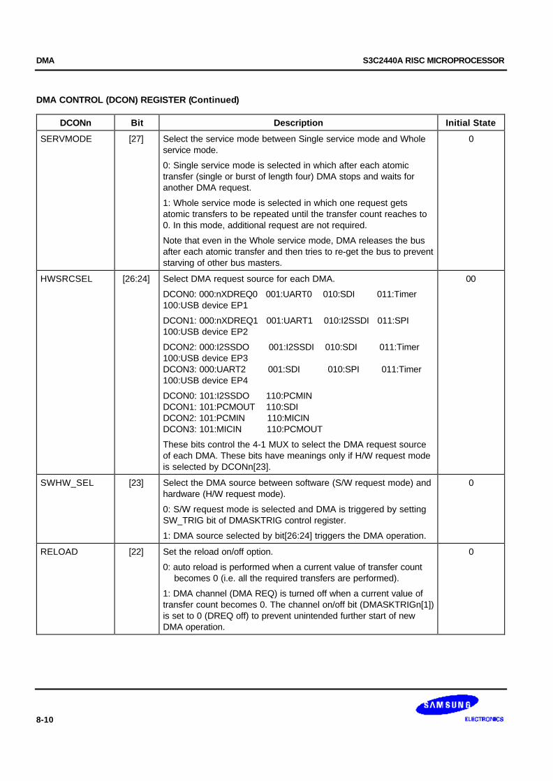
DMA S3C2440A RISC MICROPROCESSOR
8-10
DMA CONTROL (DCON) REGISTER (Continued)
DCONn Bit Description Initial State
SERVMODE [27] Select the service mode between Single service mode and Wholeservice mode.
0: Single service mode is selected in which after each atomictransfer (single or burst of length four) DMA stops and waits foranother DMA request.
1: Whole service mode is selected in which one request getsatomic transfers to be repeated until the transfer count reaches to0. In this mode, additional request are not required.
Note that even in the Whole service mode, DMA releases the busafter each atomic transfer and then tries to re-get the bus to preventstarving of other bus masters.
0
HWSRCSEL [26:24] Select DMA request source for each DMA.
DCON0: 000:nXDREQ0 001:UART0 010:SDI 011:Timer100:USB device EP1
DCON1: 000:nXDREQ1 001:UART1 010:I2SSDI 011:SPI100:USB device EP2
DCON2: 000:I2SSDO 001:I2SSDI 010:SDI 011:Timer100:USB device EP3DCON3: 000:UART2 001:SDI 010:SPI 011:Timer100:USB device EP4
DCON0: 101:I2SSDO 110:PCMINDCON1: 101:PCMOUT 110:SDIDCON2: 101:PCMIN 110:MICINDCON3: 101:MICIN 110:PCMOUT
These bits control the 4-1 MUX to select the DMA request sourceof each DMA. These bits have meanings only if H/W request modeis selected by DCONn[23].
00
SWHW_SEL [23] Select the DMA source between software (S/W request mode) andhardware (H/W request mode).
0: S/W request mode is selected and DMA is triggered by settingSW_TRIG bit of DMASKTRIG control register.
1: DMA source selected by bit[26:24] triggers the DMA operation.
0
RELOAD [22] Set the reload on/off option.
0: auto reload is performed when a current value of transfer count becomes 0 (i.e. all the required transfers are performed).
1: DMA channel (DMA REQ) is turned off when a current value oftransfer count becomes 0. The channel on/off bit (DMASKTRIGn[1])is set to 0 (DREQ off) to prevent unintended further start of newDMA operation.
0
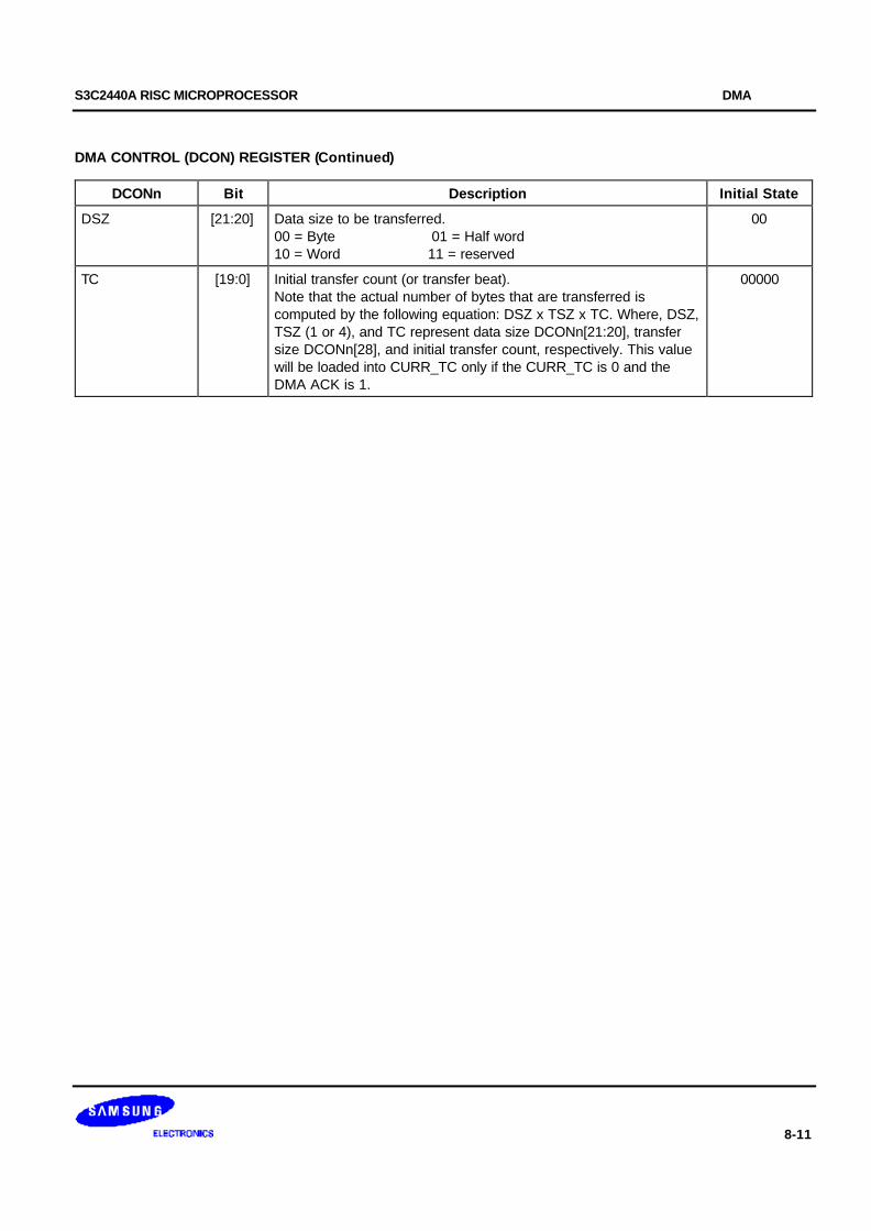
S3C2440A RISC MICROPROCESSOR DMA
8-11
DMA CONTROL (DCON) REGISTER (Continued)
DCONn Bit Description Initial State
DSZ [21:20] Data size to be transferred.00 = Byte 01 = Half word10 = Word 11 = reserved
00
TC [19:0] Initial transfer count (or transfer beat).Note that the actual number of bytes that are transferred iscomputed by the following equation: DSZ x TSZ x TC. Where, DSZ,TSZ (1 or 4), and TC represent data size DCONn[21:20], transfersize DCONn[28], and initial transfer count, respectively. This valuewill be loaded into CURR_TC only if the CURR_TC is 0 and theDMA ACK is 1.
00000

DMA S3C2440A RISC MICROPROCESSOR
8-12
DMA STATUS (DSTAT) REGISTER
Register Address R/W Description Reset Value
DSTAT0 0x4B000014 R DMA 0 count register 000000h
DSTAT1 0x4B000054 R DMA 1 count register 000000h
DSTAT2 0x4B000094 R DMA 2 count register 000000h
DSTAT3 0x4B0000D4 R DMA 3 count register 000000h
DSTATn Bit Description Initial State
STAT [21:20] Status of this DMA controller.
00: Indicates that DMA controller is ready for another DMA request.01: Indicates that DMA controller is busy for transfers.
00b
CURR_TC [19:0] Current value of transfer count.
Note that transfer count is initially set to the value of DCONn[19:0]register and decreased by one at the end of every atomic transfer.
00000h
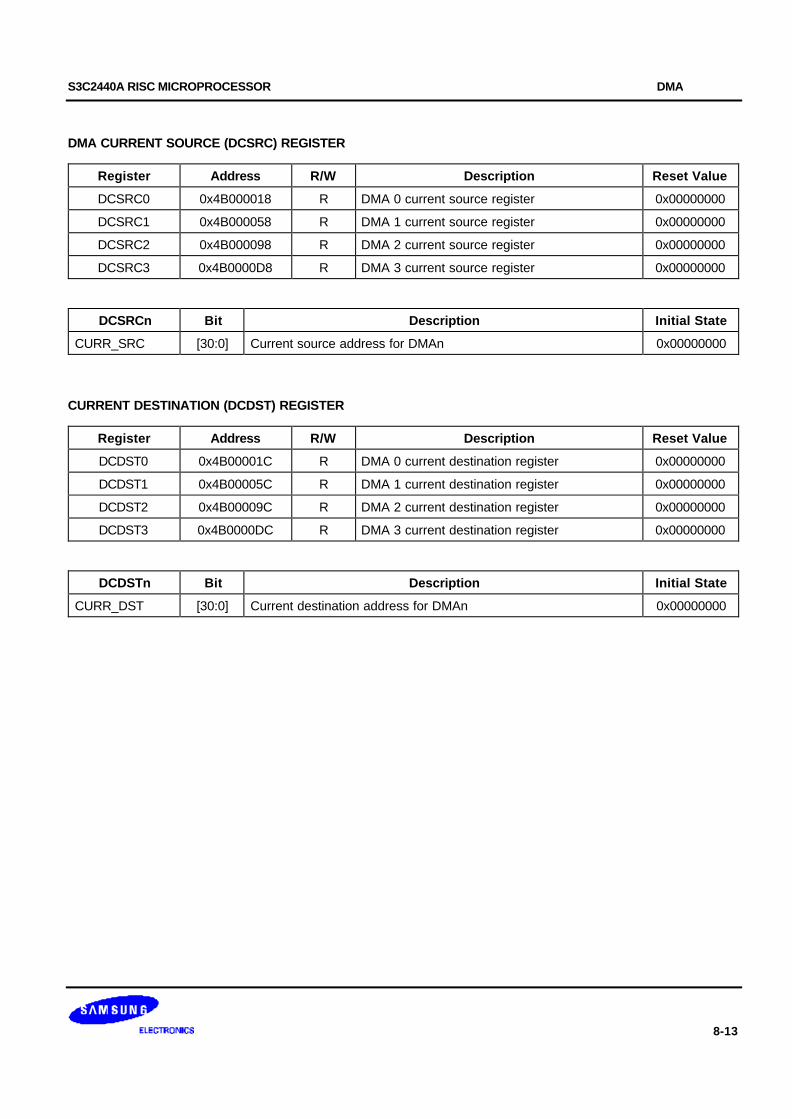
S3C2440A RISC MICROPROCESSOR DMA
8-13
DMA CURRENT SOURCE (DCSRC) REGISTER
Register Address R/W Description Reset Value
DCSRC0 0x4B000018 R DMA 0 current source register 0x00000000
DCSRC1 0x4B000058 R DMA 1 current source register 0x00000000
DCSRC2 0x4B000098 R DMA 2 current source register 0x00000000
DCSRC3 0x4B0000D8 R DMA 3 current source register 0x00000000
DCSRCn Bit Description Initial State
CURR_SRC [30:0] Current source address for DMAn 0x00000000
CURRENT DESTINATION (DCDST) REGISTER
Register Address R/W Description Reset Value
DCDST0 0x4B00001C R DMA 0 current destination register 0x00000000
DCDST1 0x4B00005C R DMA 1 current destination register 0x00000000
DCDST2 0x4B00009C R DMA 2 current destination register 0x00000000
DCDST3 0x4B0000DC R DMA 3 current destination register 0x00000000
DCDSTn Bit Description Initial State
CURR_DST [30:0] Current destination address for DMAn 0x00000000
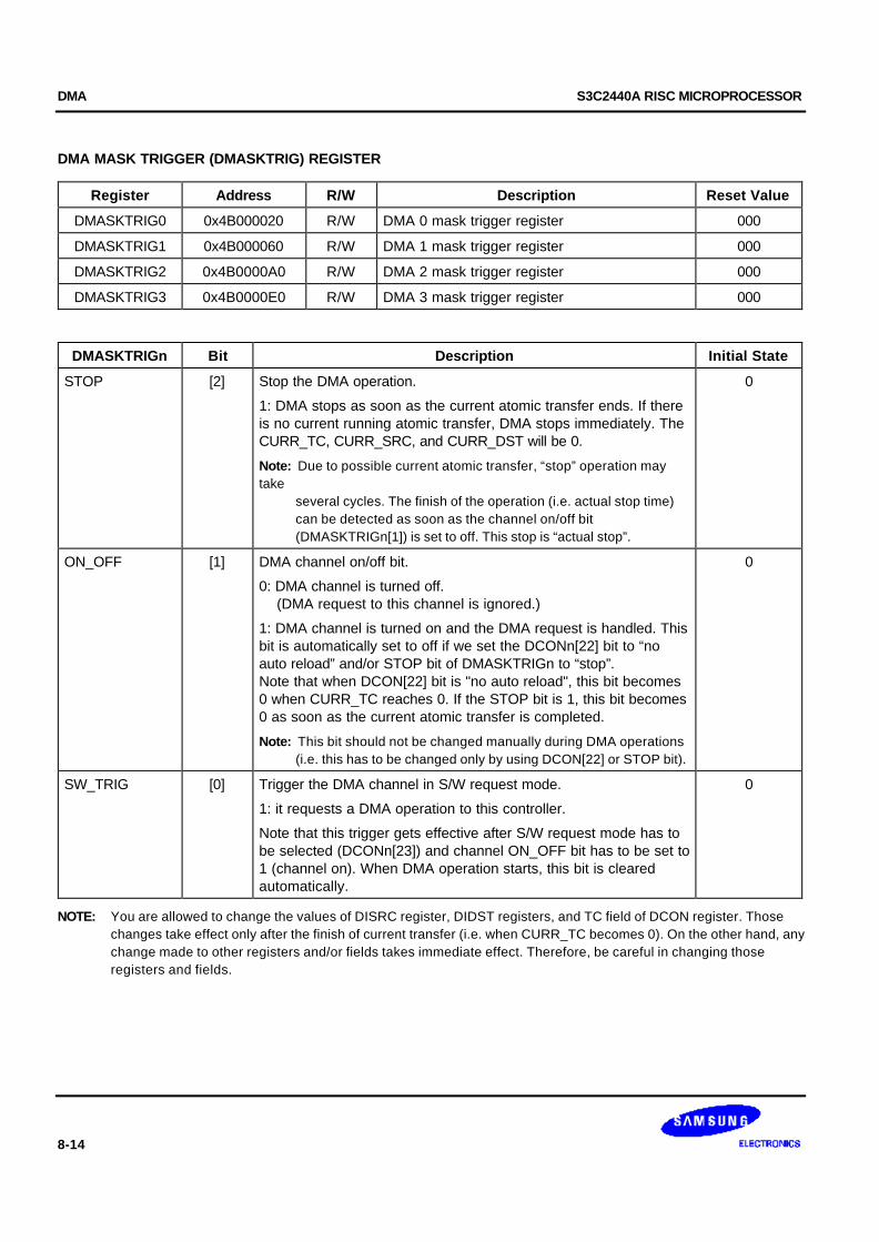
DMA S3C2440A RISC MICROPROCESSOR
8-14
DMA MASK TRIGGER (DMASKTRIG) REGISTER
Register Address R/W Description Reset Value
DMASKTRIG0 0x4B000020 R/W DMA 0 mask trigger register 000
DMASKTRIG1 0x4B000060 R/W DMA 1 mask trigger register 000
DMASKTRIG2 0x4B0000A0 R/W DMA 2 mask trigger register 000
DMASKTRIG3 0x4B0000E0 R/W DMA 3 mask trigger register 000
DMASKTRIGn Bit Description Initial State
STOP [2] Stop the DMA operation.
1: DMA stops as soon as the current atomic transfer ends. If thereis no current running atomic transfer, DMA stops immediately. TheCURR_TC, CURR_SRC, and CURR_DST will be 0.
Note: Due to possible current atomic transfer, “stop” operation maytake several cycles. The finish of the operation (i.e. actual stop time) can be detected as soon as the channel on/off bit (DMASKTRIGn[1]) is set to off. This stop is “actual stop”.
0
ON_OFF [1] DMA channel on/off bit.
0: DMA channel is turned off. (DMA request to this channel is ignored.)
1: DMA channel is turned on and the DMA request is handled. Thisbit is automatically set to off if we set the DCONn[22] bit to “noauto reload” and/or STOP bit of DMASKTRIGn to “stop”.Note that when DCON[22] bit is "no auto reload", this bit becomes0 when CURR_TC reaches 0. If the STOP bit is 1, this bit becomes0 as soon as the current atomic transfer is completed.
Note: This bit should not be changed manually during DMA operations (i.e. this has to be changed only by using DCON[22] or STOP bit).
0
SW_TRIG [0] Trigger the DMA channel in S/W request mode.
1: it requests a DMA operation to this controller.
Note that this trigger gets effective after S/W request mode has tobe selected (DCONn[23]) and channel ON_OFF bit has to be set to1 (channel on). When DMA operation starts, this bit is clearedautomatically.
0
NOTE: You are allowed to change the values of DISRC register, DIDST registers, and TC field of DCON register. Those changes take effect only after the finish of current transfer (i.e. when CURR_TC becomes 0). On the other hand, any change made to other registers and/or fields takes immediate effect. Therefore, be careful in changing those registers and fields.
S3C2440A RISC MICROPROCESSOR I/O PORTS
9-1
9 I/O PORTS
OVERVIEW
S3C2440A has 130 multi-functional input/output port pins and there are eight ports as shown below:
— Port A(GPA): 25-output port
— Port B(GPB): 11-input/out port
— Port C(GPC): 16-input/output port
— Port D(GPD): 16-input/output port
— Port E(GPE): 16-input/output port
— Port F(GPF): 8-input/output port
— Port G(GPG): 16-input/output port
— Port H(GPH): 9-input/output port
— Port J(GPJ): 13-input/output port
Each port can be easily configured by software to meet various system configurations and design requirements. Youhave to define which function of each pin is used before starting the main program. If a pin is not used for multiplexedfunctions, the pin can be configured as I/O ports.
Initial pin states are configured seamlessly to avoid problems.
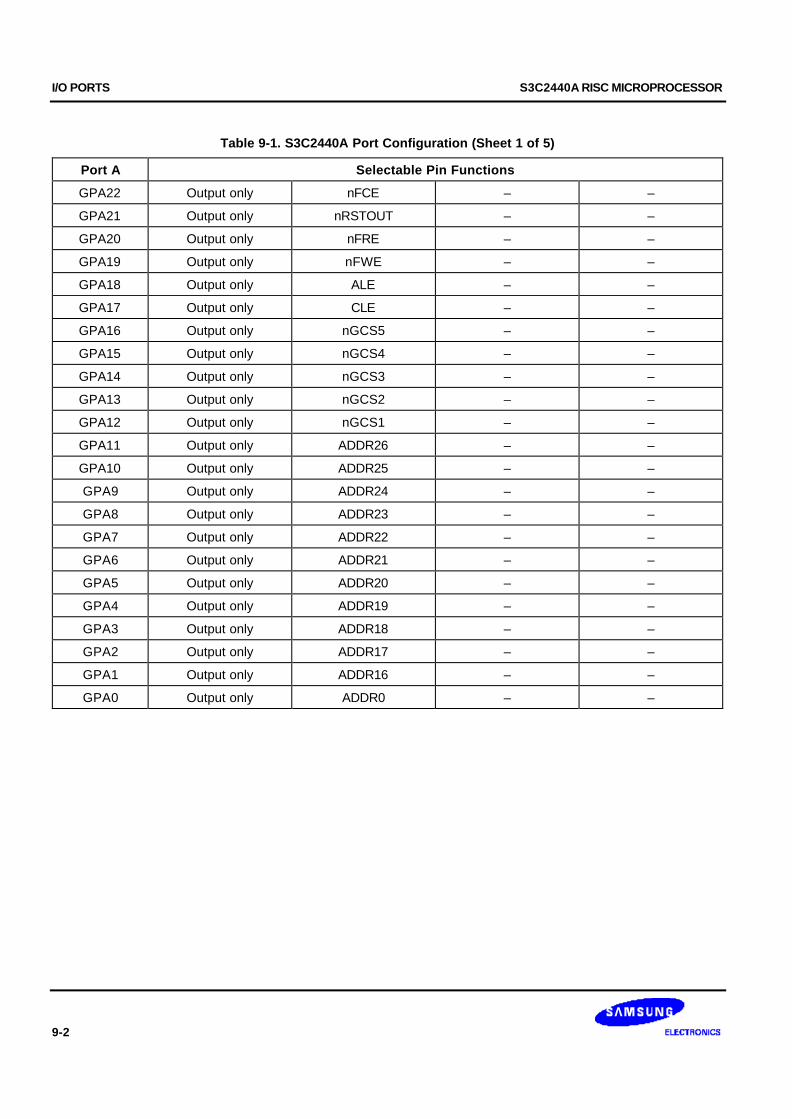
I/O PORTS S3C2440A RISC MICROPROCESSOR
9-2
Table 9-1. S3C2440A Port Configuration (Sheet 1 of 5)
Port A Selectable Pin Functions
GPA22 Output only nFCE – –
GPA21 Output only nRSTOUT – –
GPA20 Output only nFRE – –
GPA19 Output only nFWE – –
GPA18 Output only ALE – –
GPA17 Output only CLE – –
GPA16 Output only nGCS5 – –
GPA15 Output only nGCS4 – –
GPA14 Output only nGCS3 – –
GPA13 Output only nGCS2 – –
GPA12 Output only nGCS1 – –
GPA11 Output only ADDR26 – –
GPA10 Output only ADDR25 – –
GPA9 Output only ADDR24 – –
GPA8 Output only ADDR23 – –
GPA7 Output only ADDR22 – –
GPA6 Output only ADDR21 – –
GPA5 Output only ADDR20 – –
GPA4 Output only ADDR19 – –
GPA3 Output only ADDR18 – –
GPA2 Output only ADDR17 – –
GPA1 Output only ADDR16 – –
GPA0 Output only ADDR0 – –
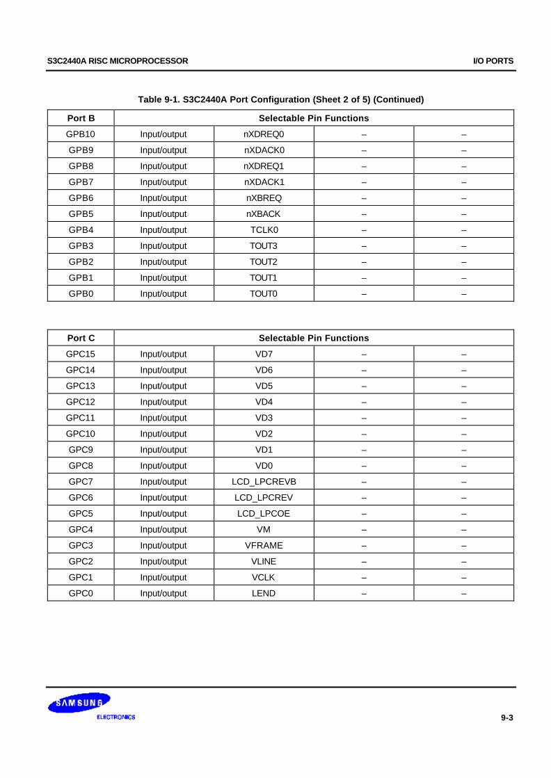
S3C2440A RISC MICROPROCESSOR I/O PORTS
9-3
Table 9-1. S3C2440A Port Configuration (Sheet 2 of 5) (Continued)
Port B Selectable Pin Functions
GPB10 Input/output nXDREQ0 – –
GPB9 Input/output nXDACK0 – –
GPB8 Input/output nXDREQ1 – –
GPB7 Input/output nXDACK1 – –
GPB6 Input/output nXBREQ – –
GPB5 Input/output nXBACK – –
GPB4 Input/output TCLK0 – –
GPB3 Input/output TOUT3 – –
GPB2 Input/output TOUT2 – –
GPB1 Input/output TOUT1 – –
GPB0 Input/output TOUT0 – –
Port C Selectable Pin Functions
GPC15 Input/output VD7 – –
GPC14 Input/output VD6 – –
GPC13 Input/output VD5 – –
GPC12 Input/output VD4 – –
GPC11 Input/output VD3 – –
GPC10 Input/output VD2 – –
GPC9 Input/output VD1 – –
GPC8 Input/output VD0 – –
GPC7 Input/output LCD_LPCREVB – –
GPC6 Input/output LCD_LPCREV – –
GPC5 Input/output LCD_LPCOE – –
GPC4 Input/output VM – –
GPC3 Input/output VFRAME – –
GPC2 Input/output VLINE – –
GPC1 Input/output VCLK – –
GPC0 Input/output LEND – –

I/O PORTS S3C2440A RISC MICROPROCESSOR
9-4
Table 9-1. S3C2440A Port Configuration (Sheet 3 of 5) (Continued)
Port D Selectable Pin Functions
GPD15 Input/output VD23 nSS0 –
GPD14 Input/output VD22 nSS1 –
GPD13 Input/output VD21 – –
GPD12 Input/output VD20 – –
GPD11 Input/output VD19 – –
GPD10 Input/output VD18 SPICLK1 –
GPD9 Input/output VD17 SPIMOSI1 –
GPD8 Input/output VD16 SPIMISO1 –
GPD7 Input/output VD15 – –
GPD6 Input/output VD14 – –
GPD5 Input/output VD13 – –
GPD4 Input/output VD12 – –
GPD3 Input/output VD11 – –
GPD2 Input/output VD10 – –
GPD1 Input/output VD9 – –
GPD0 Input/output VD8 – –
Port E Selectable Pin Functions
GPE15 Input/output IICSDA – –
GPE14 Input/output IICSCL – –
GPE13 Input/output SPICLK0 – –
GPE12 Input/output SPIMOSI0 – –
GPE11 Input/output SPIMISO0 – –
GPE10 Input/output SDDAT3 – –
GPE9 Input/output SDDAT2 – –
GPE8 Input/output SDDAT1 – –
GPE7 Input/output SDDAT0 – –
GPE6 Input/output SDCMD – –
GPE5 Input/output SDCLK – –
GPE4 Input/output I2SSDO AC_SDATA_OUT –
GPE3 Input/output I2SSDI AC_SDATA_IN –
GPE2 Input/output CDCLK AC_nRESET –
GPE1 Input/output I2SSCLK AC_BIT_CLK –
GPE0 Input/output I2SLRCK AC_SYNC –

S3C2440A RISC MICROPROCESSOR I/O PORTS
9-5
Table 9-1. S3C2440A Port Configuration (Sheet 4 of 5) (Continued)
Port F Selectable Pin Functions
GPF7 Input/output EINT7 – –
GPF6 Input/output EINT6 – –
GPF5 Input/output EINT5 – –
GPF4 Input/output EINT4 – –
GPF3 Input/output EINT3 – –
GPF2 Input/output EINT2
GPF1 Input/output EINT1
GPF0 Input/output EINT0
Port G Selectable Pin Functions
GPG15 Input/output EINT23 – –
GPG14 Input/output EINT22 – –
GPG13 Input/output EINT21 – –
GPG12 Input/output EINT20 – –
GPG11 Input/output EINT19 TCLK1 –
GPG10 Input/output EINT18 nCTS1 –
GPG9 Input/output EINT17 nRTS1 –
GPG8 Input/output EINT16 – –
GPG7 Input/output EINT15 SPICLK1 –
GPG6 Input/output EINT14 SPIMOSI1 –
GPG5 Input/output EINT13 SPIMISO1 –
GPG4 Input/output EINT12 LCD_PWREN –
GPG3 Input/output EINT11 nSS1 –
GPG2 Input/output EINT10 nSS0 –
GPG1 Input/output EINT9 – –
GPG0 Input/output EINT8 – –

I/O PORTS S3C2440A RISC MICROPROCESSOR
9-6
Table 9-1. S3C2440A Port Configuration (Sheet 5 of 5) (Continued)
Port H Selectable Pin Functions
GPH10 Input/output CLKOUT1 – –
GPH9 Input/output CLKOUT0 – –
GPH8 Input/output UEXTCLK – –
GPH7 Input/output RXD2 nCTS1 –
GPH6 Input/output TXD2 nRTS1 –
GPH5 Input/output RXD1 – –
GPH4 Input/output TXD1 – –
GPH3 Input/output RXD0 – –
GPH2 Input/output TXD0 – –
GPH1 Input/output nRTS0 – –
GPH0 Input/output nCTS0 – –
Port J Selectable Pin Functions
GPJ12 Input/output CAMRESET – –
GPJ11 Input/output CAMCLKOUT – –
GPJ10 Input/output CAMHREF – –
GPJ9 Input/output CAMVSYNC – –
GPJ8 Input/output CAMPCLK – –
GPJ7 Input/output CAMDATA7 – –
GPJ6 Input/output CAMDATA6 – –
GPJ5 Input/output CAMDATA5 – –
GPJ4 Input/output CAMDATA4 – –
GPJ3 Input/output CAMDATA3 – –
GPJ2 Input/output CAMDATA2 – –
GPJ1 Input/output CAMDATA1 – –
GPJ0 Input/output CAMDATA0 – –
S3C2440A RISC MICROPROCESSOR I/O PORTS
9-7
PORT CONTROL DESCRIPTIONS
PORT CONFIGURATION REGISTER (GPACON-GPJCON)
In S3C2440A, most of the pins are multiplexed pins. So, It is determined which function is selected for each pins.The PnCON(port control register) determines which function is used for each pin.
If PE0 – PE7 is used for the wakeup signal in power down mode, these ports must be configured in interrupt mode.
PORT DATA REGISTER (GPADAT-GPJDAT)
If Ports are configured as output ports, data can be written to the corresponding bit of PnDAT. If Ports are configuredas input ports, the data can be read from the corresponding bit of PnDAT.
PORT PULL-UP REGISTER (GPBUP-GPJUP)
The port pull-up register controls the pull-up resister enable/disable of each port group. When the corresponding bit is0, the pull-up resister of the pin is enabled. When 1, the pull-up resister is disabled.
If the port pull-up register is enabled then the pull-up resisters work without pin’s functional setting(input, output,DATAn, EINTn and etc)
MISCELLANEOUS CONTROL REGISTER
This register controls DATA port pull-up resister in Sleep mode, USB pad, and CLKOUT selection.
EXTERNAL INTERRUPT CONTROL REGISTER
The 24 external interrupts are requested by various signaling methods. The EXTINT register configures the signalingmethod among the low level trigger, high level trigger, falling edge trigger, rising edge trigger, and both edge triggerfor the external interrupt request
Because each external interrupt pin has a digital filter, the interrupt controller can recognize the request signal that islonger than 3 clocks.
EINT[15:0] are used for wakeup sources.

I/O PORTS S3C2440A RISC MICROPROCESSOR
9-8
I/O PORT CONTROL REGISTER
PORT A CONTROL REGISTERS (GPACON, GPADAT)
Register Address R/W Description Reset Value
GPACON 0x56000000 R/W Configures the pins of port A 0xffffff
GPADAT 0x56000004 R/W The data register for port A Undef.
Reserved 0x56000008 – Reserved Undef
Reserved 0x5600000c – Reserved Undef
GPACON Bit Description
GPA24 [24] Reserved
GPA23 [23] Reserved
GPA22 [22] 0 = Output 1 = nFCE
GPA21 [21] 0 = Output 1 = nRSTOUT
GPA20 [20] 0 = Output 1 = nFRE
GPA19 [19] 0 = Output 1 = nFWE
GPA18 [18] 0 = Output 1 = ALE
GPA17 [17] 0 = Output 1 = CLE
GPA16 [16] 0 = Output 1 = nGCS[5]
GPA15 [15] 0 = Output 1 = nGCS[4]
GPA14 [14] 0 = Output 1 = nGCS[3]
GPA13 [13] 0 = Output 1 = nGCS[2]
GPA12 [12] 0 = Output 1 = nGCS[1]
GPA11 [11] 0 = Output 1 = ADDR26
GPA10 [10] 0 = Output 1 = ADDR25
GPA9 [9] 0 = Output 1 = ADDR24
GPA8 [8] 0 = Output 1 = ADDR23
GPA7 [7] 0 = Output 1 = ADDR22
GPA6 [6] 0 = Output 1 = ADDR21
GPA5 [5] 0 = Output 1 = ADDR20
GPA4 [4] 0 = Output 1 = ADDR19
GPA3 [3] 0 = Output 1 = ADDR18
GPA2 [2] 0 = Output 1 = ADDR17
GPA1 [1] 0 = Output 1 = ADDR16
GPA0 [0] 0 = Output 1 = ADDR0
NOTE: The GPA21 signal level depends on VDDOP, the other pads (GPA0~20, GPA22~24) are all on VDDMOP.

S3C2440A RISC MICROPROCESSOR I/O PORTS
9-9

I/O PORTS S3C2440A RISC MICROPROCESSOR
9-10
PORT A CONTROL REGISTERS (GPACON, GPADAT) (Continued)
GPADAT Bit Description
GPA[24:0] [24:0] When the port is configured as output port, the pin state is the same as thecorresponding bit.
When the port is configured as functional pin, the undefined value will beread.
NOTE: nRSTOUT = nRESET & nWDTRST & SW_RESET

S3C2440A RISC MICROPROCESSOR I/O PORTS
9-11
PORT B CONTROL REGISTERS (GPBCON, GPBDAT, GPBUP)
Register Address R/W Description Reset Value
GPBCON 0x56000010 R/W Configures the pins of port B 0x0
GPBDAT 0x56000014 R/W The data register for port B Undef.
GPBUP 0x56000018 R/W Pull-up disable register for port B 0x0
Reserved 0x5600001c
PBCON Bit Description
GPB10 [21:20] 00 = Input 01 = Output10 = nXDREQ0 11 = reserved
GPB9 [19:18] 00 = Input 01 = Output10 = nXDACK0 11 = reserved
GPB8 [17:16] 00 = Input 01 = Output10 = nXDREQ1 11 = Reserved
GPB7 [15:14] 00 = Input 01 = Output10 = nXDACK1 11 = Reserved
GPB6 [13:12] 00 = Input 01 = Output10 = nXBREQ 11 = reserved
GPB5 [11:10] 00 = Input 01 = Output10 = nXBACK 11 = reserved
GPB4 [9:8] 00 = Input 01 = Output10 = TCLK [0] 11 = reserved
GPB3 [7:6] 00 = Input 01 = Output10 = TOUT3 11 = reserved
GPB2 [5:4] 00 = Input 01 = Output10 = TOUT2 11 = reserved]
GPB1 [3:2] 00 = Input 01 = Output10 = TOUT1 11 = reserved
GPB0 [1:0] 00 = Input 01 = Output10 = TOUT0 11 = reserved
GPBDAT Bit Description
GPB[10:0] [10:0] When the port is configured as input port, the corresponding bit is the pinstate. When the port is configured as output port, the pin state is the sameas the corresponding bit. When the port is configured as functional pin, theundefined value will be read.
GPBUP Bit Description
GPB[10:0] [10:0] 0: The pull up function attached to the corresponding port pin is enabled.1: The pull up function is disabled.
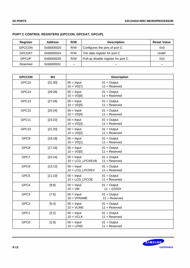
I/O PORTS S3C2440A RISC MICROPROCESSOR
9-12
PORT C CONTROL REGISTERS (GPCCON, GPCDAT, GPCUP)
Register Address R/W Description Reset Value
GPCCON 0x56000020 R/W Configures the pins of port C 0x0
GPCDAT 0x56000024 R/W The data register for port C Undef.
GPCUP 0x56000028 R/W Pull-up disable register for port C 0x0
Reserved 0x5600002c – – –
GPCCON Bit Description
GPC15 [31:30] 00 = Input 01 = Output10 = VD[7] 11 = Reserved
GPC14 [29:28] 00 = Input 01 = Output10 = VD[6] 11 = Reserved
GPC13 [27:26] 00 = Input 01 = Output10 = VD[5] 11 = Reserved
GPC12 [25:24] 00 = Input 01 = Output10 = VD[4] 11 = Reserved
GPC11 [23:22] 00 = Input 01 = Output10 = VD[3] 11 = Reserved
GPC10 [21:20] 00 = Input 01 = Output10 = VD[2] 11 = Reserved
GPC9 [19:18] 00 = Input 01 = Output10 = VD[1] 11 = Reserved
GPC8 [17:16] 00 = Input 01 = Output10 = VD[0] 11 = Reserved
GPC7 [15:14] 00 = Input 01 = Output10 = LCD_LPCREVB 11 = Reserved
GPC6 [13:12] 00 = Input 01 = Output10 = LCD_LPCREV 11 = Reserved
GPC5 [11:10] 00 = Input 01 = Output10 = LCD_LPCOE 11 = Reserved
GPC4 [9:8] 00 = Input 01 = Output10 = VM 11 = I2SSDI
GPC3 [7:6] 00 = Input 01 = Output10 = VFRAME 11 = Reserved
GPC2 [5:4] 00 = Input 01 = Output10 = VLINE 11 = Reserved
GPC1 [3:2] 00 = Input 01 = Output10 = VCLK 11 = Reserved
GPC0 [1:0] 00 = Input 01 = Output10 = LEND 11 = Reserved

S3C2440A RISC MICROPROCESSOR I/O PORTS
9-13
PORT C CONTROL REGISTERS (GPCCON, GPCDAT, GPCUP) (Continued)
GPCDAT Bit Description
GPC[15:0] [15:0] When the port is configured as input port, the corresponding bit is the pinstate. When the port is configured as output port, the pin state is the sameas the corresponding bit.
When the port is configured as functional pin, the undefined value will beread.
GPCUP Bit Description
GPC[15:0] [15:0] 0: The pull up function attached to the corresponding port pin is enabled.1: The pull up function is disabled.

I/O PORTS S3C2440A RISC MICROPROCESSOR
9-14
PORT D CONTROL REGISTERS (GPDCON, GPDDAT, GPDUP)
Register Address R/W Description Reset Value
GPDCON 0x56000030 R/W Configures the pins of port D 0x0
GPDDAT 0x56000034 R/W The data register for port D Undef.
GPDUP 0x56000038 R/W Pull-up disable register for port D 0xf000
Reserved 0x5600003c – – –
GPDCON Bit Description
GPD15 [31:30] 00 = Input 01 = Output10 = VD[23] 11 = nSS0
GPD14 [29:28] 00 = Input 01 = Output10 = VD[22] 11 = nSS1
GPD13 [27:26] 00 = Input 01 = Output10 = VD[21] 11 = Reserved
GPD12 [25:24] 00 = Input 01 = Output10 = VD[20] 11 = Reserved
GPD11 [23:22] 00 = Input 01 = Output10 = VD[19] 11 = Reserved
GPD10 [21:20] 00 = Input 01 = Output10 = VD[18] 11 = SPICLK1
GPD9 [19:18] 00 = Input 01 = Output10 = VD[17] 11 = SPIMOSI1
GPD8 [17:16] 00 = Input 01 = Output10 = VD[16] 11 = SPIMISO1
GPD7 [15:14] 00 = Input 01 = Output10 = VD[15] 11 = Reserved
GPD6 [13:12] 00 = Input 01 = Output10 = VD[14] 11 = Reserved
GPD5 [11:10] 00 = Input 01 = Output10 = VD[13] 11 = Reserved
GPD4 [9:8] 00 = Input 01 = Output10 = VD[12] 11 = Reserved
GPD3 [7:6] 00 = Input 01 = Output10 = VD[11] 11 = Reserved
GPD2 [5:4] 00 = Input 01 = Output10 = VD[10] 11 = Reserved
GPD1 [3:2] 00 = Input 01 = Output10 = VD[9] 11 = Reserved
GPD0 [1:0] 00 = Input 01 = Output10 = VD[8] 11 = Reserved
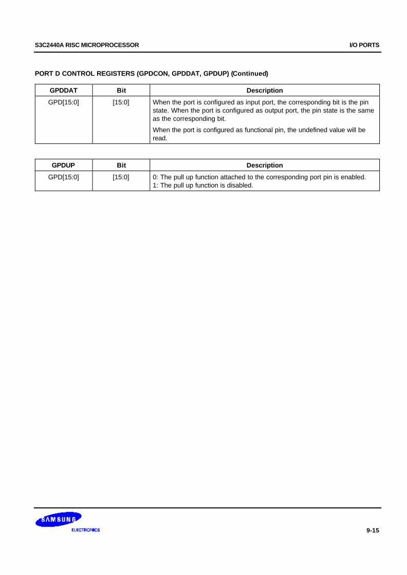
S3C2440A RISC MICROPROCESSOR I/O PORTS
9-15
PORT D CONTROL REGISTERS (GPDCON, GPDDAT, GPDUP) (Continued)
GPDDAT Bit Description
GPD[15:0] [15:0] When the port is configured as input port, the corresponding bit is the pinstate. When the port is configured as output port, the pin state is the sameas the corresponding bit.
When the port is configured as functional pin, the undefined value will beread.
GPDUP Bit Description
GPD[15:0] [15:0] 0: The pull up function attached to the corresponding port pin is enabled.1: The pull up function is disabled.

I/O PORTS S3C2440A RISC MICROPROCESSOR
9-16
PORT E CONTROL REGISTERS (GPECON, GPEDAT, GPEUP)
Register Address R/W Description Reset Value
GPECON 0x56000040 R/W Configures the pins of port E 0x0
GPEDAT 0x56000044 R/W The data register for port E Undef.
GPEUP 0x56000048 R/W Pull-up disable register for port E 0x0000
Reserved 0x5600004c – – –
GPECON Bit Description
GPE15 [31:30] 00 = Input 01 = Output10 = IICSDA 11 = ReservedThis pad is open-drain, There is no Pull-up option.
GPE14 [29:28] 00 = Input 01 = Output10 = IICSCL 11 = ReservedThis pad is open-drain, There is no Pull-up option.
GPE13 [27:26] 00 = Input 01 = Output10 = SPICLK0 11 = Reserved
GPE12 [25:24] 00 = Input 01 = Output10 = SPIMOSI0 11 = Reserved
GPE11 [23:22] 00 = Input 01 = Output10 = SPIMISO0 11 = Reserved
GPE10 [21:20] 00 = Input 01 = Output10 = SDDAT3 11 = Reserved
GPE9 [19:18] 00 = Input 01 = Output10 = SDDAT2 11 = Reserved
GPE8 [17:16] 00 = Input 01 = Output10 = SDDAT1 11 = Reserved
GPE7 [15:14] 00 = Input 01 = Output10 = SDDAT0 11 = Reserved
GPE6 [13:12] 00 = Input 01 = Output10 = SDCMD 11 = Reserved
GPE5 [11:10] 00 = Input 01 = Output10 = SDCLK 11 = Reserved
GPE4 [9:8] 00 = Input 01 = Output10 = I2SDO 11 = AC_SDATA_OUT
GPE3 [7:6] 00 = Input 01 = Output10 = I2SDI 11 = AC_SDATA_IN
GPE2 [5:4] 00 = Input 01 = Output10 = CDCLK 11 = AC_nRESET
GPE1 [3:2] 00 = Input 01 = Output10 = I2SSCLK 11 = AC_BIT_CLK
GPE0 [1:0] 00 = Input 01 = Output10 = I2SLRCK 11 = AC_SYNC

S3C2440A RISC MICROPROCESSOR I/O PORTS
9-17
PORT E CONTROL REGISTERS (GPECON, GPEDAT, GPEUP) (Continued)
GPEDAT Bit Description
GPE[15:0] [15:0] When the port is configured as an input port, the corresponding bit is thepin state. When the port is configured as an output port, the pin state is thesame as the corresponding bit.
When the port is configured as a functional pin, the undefined value will beread.
GPEUP Bit Description
GPE[13:0] [13:0] 0: The pull up function attached to the corresponding port pin is enabled.1: The pull up function is disabled.

I/O PORTS S3C2440A RISC MICROPROCESSOR
9-18
PORT F CONTROL REGISTERS (GPFCON, GPFDAT)
If GPF0–GPF7 will be used for wake-up signals at power down mode, the ports will be set in interrupt mode.
Register Address R/W Description Reset Value
GPFCON 0x56000050 R/W Configures the pins of port F 0x0
GPFDAT 0x56000054 R/W The data register for port F Undef.
GPFUP 0x56000058 R/W Pull-up disable register for port F 0x000
Reserved 0x5600005c – – –
GPFCON Bit Description
GPF7 [15:14] 00 = Input 01 = Output10 = EINT[7] 11 = Reserved
GPF6 [13:12] 00 = Input 01 = Output10 = EINT[6] 11 = Reserved
GPF5 [11:10] 00 = Input 01 = Output10 = EINT[5] 11 = Reserved
GPF4 [9:8] 00 = Input 01 = Output10 = EINT[4] 11 = Reserved
GPF3 [7:6] 00 = Input 01 = Output10 = EINT[3] 11 = Reserved
GPF2 [5:4] 00 = Input 01 = Output10 = EINT2] 11 = Reserved
GPF1 [3:2] 00 = Input 01 = Output10 = EINT[1] 11 = Reserved
GPF0 [1:0] 00 = Input 01 = Output10 = EINT[0] 11 = Reserved
GPFDAT Bit Description
GPF[7:0] [7:0] When the port is configured as an input port, the corresponding bit is thepin state. When the port is configured as an output port, the pin state is thesame as the corresponding bit.
When the port is configured as functional pin, the undefined value will beread.
GPFUP Bit Description
GPF[7:0] [7:0] 0: The pull up function attached to the corresponding port pin is enabled.1: The pull up function is disabled.
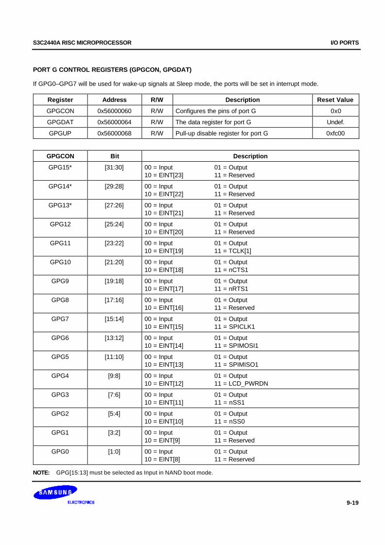
S3C2440A RISC MICROPROCESSOR I/O PORTS
9-19
PORT G CONTROL REGISTERS (GPGCON, GPGDAT)
If GPG0–GPG7 will be used for wake-up signals at Sleep mode, the ports will be set in interrupt mode.
Register Address R/W Description Reset Value
GPGCON 0x56000060 R/W Configures the pins of port G 0x0
GPGDAT 0x56000064 R/W The data register for port G Undef.
GPGUP 0x56000068 R/W Pull-up disable register for port G 0xfc00
GPGCON Bit Description
GPG15* [31:30] 00 = Input 01 = Output10 = EINT[23] 11 = Reserved
GPG14* [29:28] 00 = Input 01 = Output10 = EINT[22] 11 = Reserved
GPG13* [27:26] 00 = Input 01 = Output10 = EINT[21] 11 = Reserved
GPG12 [25:24] 00 = Input 01 = Output10 = EINT[20] 11 = Reserved
GPG11 [23:22] 00 = Input 01 = Output10 = EINT[19] 11 = TCLK[1]
GPG10 [21:20] 00 = Input 01 = Output10 = EINT[18] 11 = nCTS1
GPG9 [19:18] 00 = Input 01 = Output10 = EINT[17] 11 = nRTS1
GPG8 [17:16] 00 = Input 01 = Output10 = EINT[16] 11 = Reserved
GPG7 [15:14] 00 = Input 01 = Output10 = EINT[15] 11 = SPICLK1
GPG6 [13:12] 00 = Input 01 = Output10 = EINT[14] 11 = SPIMOSI1
GPG5 [11:10] 00 = Input 01 = Output10 = EINT[13] 11 = SPIMISO1
GPG4 [9:8] 00 = Input 01 = Output10 = EINT[12] 11 = LCD_PWRDN
GPG3 [7:6] 00 = Input 01 = Output10 = EINT[11] 11 = nSS1
GPG2 [5:4] 00 = Input 01 = Output10 = EINT[10] 11 = nSS0
GPG1 [3:2] 00 = Input 01 = Output10 = EINT[9] 11 = Reserved
GPG0 [1:0] 00 = Input 01 = Output10 = EINT[8] 11 = Reserved
NOTE: GPG[15:13] must be selected as Input in NAND boot mode.
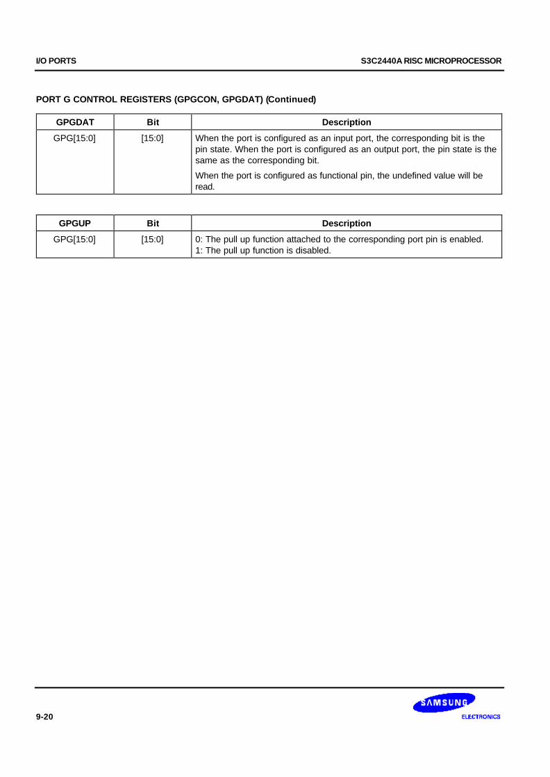
I/O PORTS S3C2440A RISC MICROPROCESSOR
9-20
PORT G CONTROL REGISTERS (GPGCON, GPGDAT) (Continued)
GPGDAT Bit Description
GPG[15:0] [15:0] When the port is configured as an input port, the corresponding bit is thepin state. When the port is configured as an output port, the pin state is thesame as the corresponding bit.
When the port is configured as functional pin, the undefined value will beread.
GPGUP Bit Description
GPG[15:0] [15:0] 0: The pull up function attached to the corresponding port pin is enabled.1: The pull up function is disabled.
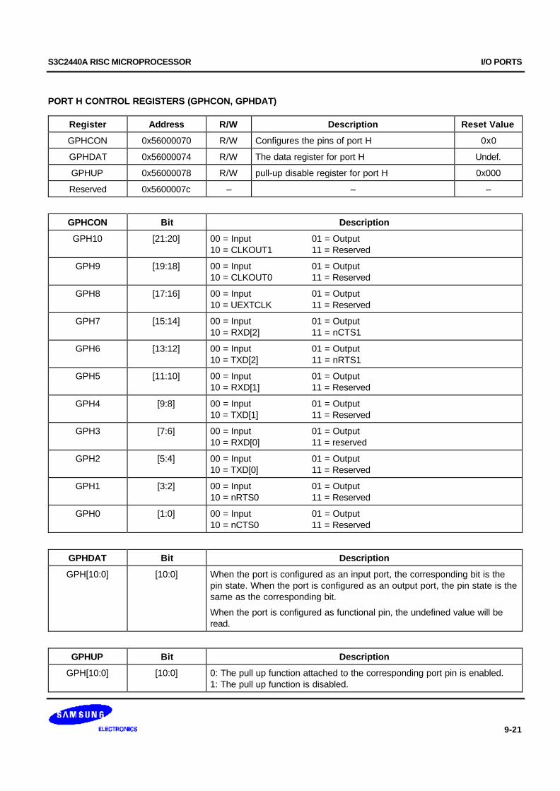
S3C2440A RISC MICROPROCESSOR I/O PORTS
9-21
PORT H CONTROL REGISTERS (GPHCON, GPHDAT)
Register Address R/W Description Reset Value
GPHCON 0x56000070 R/W Configures the pins of port H 0x0
GPHDAT 0x56000074 R/W The data register for port H Undef.
GPHUP 0x56000078 R/W pull-up disable register for port H 0x000
Reserved 0x5600007c – – –
GPHCON Bit Description
GPH10 [21:20] 00 = Input 01 = Output10 = CLKOUT1 11 = Reserved
GPH9 [19:18] 00 = Input 01 = Output10 = CLKOUT0 11 = Reserved
GPH8 [17:16] 00 = Input 01 = Output10 = UEXTCLK 11 = Reserved
GPH7 [15:14] 00 = Input 01 = Output10 = RXD[2] 11 = nCTS1
GPH6 [13:12] 00 = Input 01 = Output10 = TXD[2] 11 = nRTS1
GPH5 [11:10] 00 = Input 01 = Output10 = RXD[1] 11 = Reserved
GPH4 [9:8] 00 = Input 01 = Output10 = TXD[1] 11 = Reserved
GPH3 [7:6] 00 = Input 01 = Output10 = RXD[0] 11 = reserved
GPH2 [5:4] 00 = Input 01 = Output10 = TXD[0] 11 = Reserved
GPH1 [3:2] 00 = Input 01 = Output10 = nRTS0 11 = Reserved
GPH0 [1:0] 00 = Input 01 = Output10 = nCTS0 11 = Reserved
GPHDAT Bit Description
GPH[10:0] [10:0] When the port is configured as an input port, the corresponding bit is thepin state. When the port is configured as an output port, the pin state is thesame as the corresponding bit.
When the port is configured as functional pin, the undefined value will beread.
GPHUP Bit Description
GPH[10:0] [10:0] 0: The pull up function attached to the corresponding port pin is enabled.1: The pull up function is disabled.
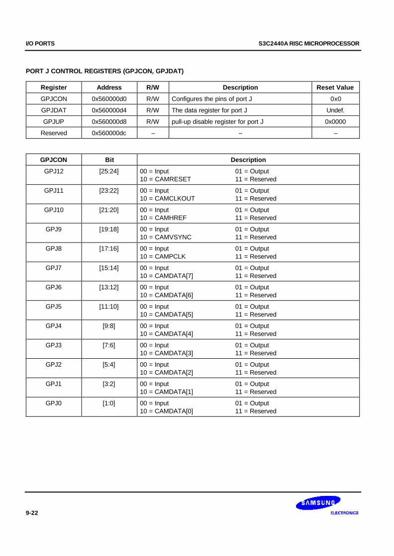
I/O PORTS S3C2440A RISC MICROPROCESSOR
9-22
PORT J CONTROL REGISTERS (GPJCON, GPJDAT)
Register Address R/W Description Reset Value
GPJCON 0x560000d0 R/W Configures the pins of port J 0x0
GPJDAT 0x560000d4 R/W The data register for port J Undef.
GPJUP 0x560000d8 R/W pull-up disable register for port J 0x0000
Reserved 0x560000dc – – –
GPJCON Bit Description
GPJ12 [25:24] 00 = Input 01 = Output10 = CAMRESET 11 = Reserved
GPJ11 [23:22] 00 = Input 01 = Output10 = CAMCLKOUT 11 = Reserved
GPJ10 [21:20] 00 = Input 01 = Output10 = CAMHREF 11 = Reserved
GPJ9 [19:18] 00 = Input 01 = Output10 = CAMVSYNC 11 = Reserved
GPJ8 [17:16] 00 = Input 01 = Output10 = CAMPCLK 11 = Reserved
GPJ7 [15:14] 00 = Input 01 = Output10 = CAMDATA[7] 11 = Reserved
GPJ6 [13:12] 00 = Input 01 = Output10 = CAMDATA[6] 11 = Reserved
GPJ5 [11:10] 00 = Input 01 = Output10 = CAMDATA[5] 11 = Reserved
GPJ4 [9:8] 00 = Input 01 = Output10 = CAMDATA[4] 11 = Reserved
GPJ3 [7:6] 00 = Input 01 = Output10 = CAMDATA[3] 11 = Reserved
GPJ2 [5:4] 00 = Input 01 = Output10 = CAMDATA[2] 11 = Reserved
GPJ1 [3:2] 00 = Input 01 = Output10 = CAMDATA[1] 11 = Reserved
GPJ0 [1:0] 00 = Input 01 = Output10 = CAMDATA[0] 11 = Reserved
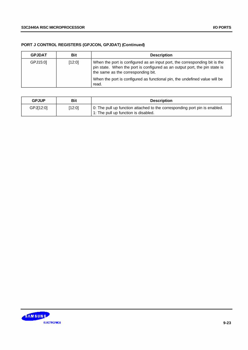
S3C2440A RISC MICROPROCESSOR I/O PORTS
9-23
PORT J CONTROL REGISTERS (GPJCON, GPJDAT) (Continued)
GPJDAT Bit Description
GPJ15:0] [12:0] When the port is configured as an input port, the corresponding bit is thepin state. When the port is configured as an output port, the pin state isthe same as the corresponding bit.
When the port is configured as functional pin, the undefined value will beread.
GPJUP Bit Description
GPJ[12:0] [12:0] 0: The pull up function attached to the corresponding port pin is enabled.1: The pull up function is disabled.
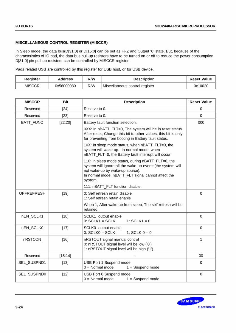
I/O PORTS S3C2440A RISC MICROPROCESSOR
9-24
MISCELLANEOUS CONTROL REGISTER (MISCCR)
In Sleep mode, the data bus(D[31:0] or D[15:0] can be set as Hi-Z and Output ‘0’ state. But, because of thecharacteristics of IO pad, the data bus pull-up resisters have to be turned on or off to reduce the power consumption.D[31:0] pin pull-up resisters can be controlled by MISCCR register.
Pads related USB are controlled by this register for USB host, or for USB device.
Register Address R/W Description Reset Value
MISCCR 0x56000080 R/W Miscellaneous control register 0x10020
MISCCR Bit Description Reset Value
Reserved [24] Reserve to 0. 0
Reserved [23] Reserve to 0. 0
BATT_FUNC [22:20] Battery fault function selection.
0XX: In nBATT_FLT=0, The system will be in reset status.After reset, Change this bit to other values, this bit is onlyfor preventing from booting in Battery fault status.
10X: In sleep mode status, when nBATT_FLT=0, thesystem will wake-up. In normal mode, whennBATT_FLT=0, the Battery fault interrupt will occur.
110: In sleep mode status, during nBATT_FLT=0, thesystem will ignore all the wake-up events(the system willnot wake-up by wake-up source).In normal mode, nBATT_FLT signal cannot affect thesystem.
111: nBATT_FLT function disable.
000
OFFREFRESH [19] 0: Self refresh retain disable1: Self refresh retain enable
When 1, After wake-up from sleep, The self-refresh will beretained.
0
nEN_SCLK1 [18] SCLK1 output enable0: SCLK1 = SCLK 1: SCLK1 = 0
0
nEN_SCLK0 [17] SCLK0 output enable0: SCLK0 = SCLK 1: SCLK 0 = 0
0
nRSTCON [16] nRSTOUT signal manual control0: nRSTOUT signal level will be low (‘0’)1: nRSTOUT signal level will be high (‘1’)
1
Reserved [15:14] – 00
SEL_SUSPND1 [13] USB Port 1 Suspend mode0 = Normal mode 1 = Suspend mode
0
SEL_SUSPND0 [12] USB Port 0 Suspend mode0 = Normal mode 1 = Suspend mode
0
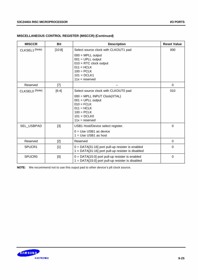
S3C2440A RISC MICROPROCESSOR I/O PORTS
9-25
MISCELLANEOUS CONTROL REGISTER (MISCCR) (Continued)
MISCCR Bit Description Reset Value
CLKSEL1 (Note) [10:8] Select source clock with CLKOUT1 pad
000 = MPLL output001 = UPLL output010 = RTC clock output011 = HCLK100 = PCLK101 = DCLK111x = reserved
000
Reserved [7] – 0
CLKSEL0 (Note) [6:4] Select source clock with CLKOUT0 pad
000 = MPLL INPUT Clock(XTAL)001 = UPLL output010 = FCLK011 = HCLK100 = PCLK101 = DCLK011x = reserved
010
SEL_USBPAD [3] USB1 Host/Device select register.
0 = Use USB1 as device1 = Use USB1 as host
0
Reserved [2] Reserved 0
SPUCR1 [1] 0 = DATA[31:16] port pull-up resister is enabled1 = DATA[31:16] port pull-up resister is disabled
0
SPUCR0 [0] 0 = DATA[15:0] port pull-up resister is enabled1 = DATA[15:0] port pull-up resister is disabled
0
NOTE: We recommend not to use this ouput pad to other device’s pll clock source.
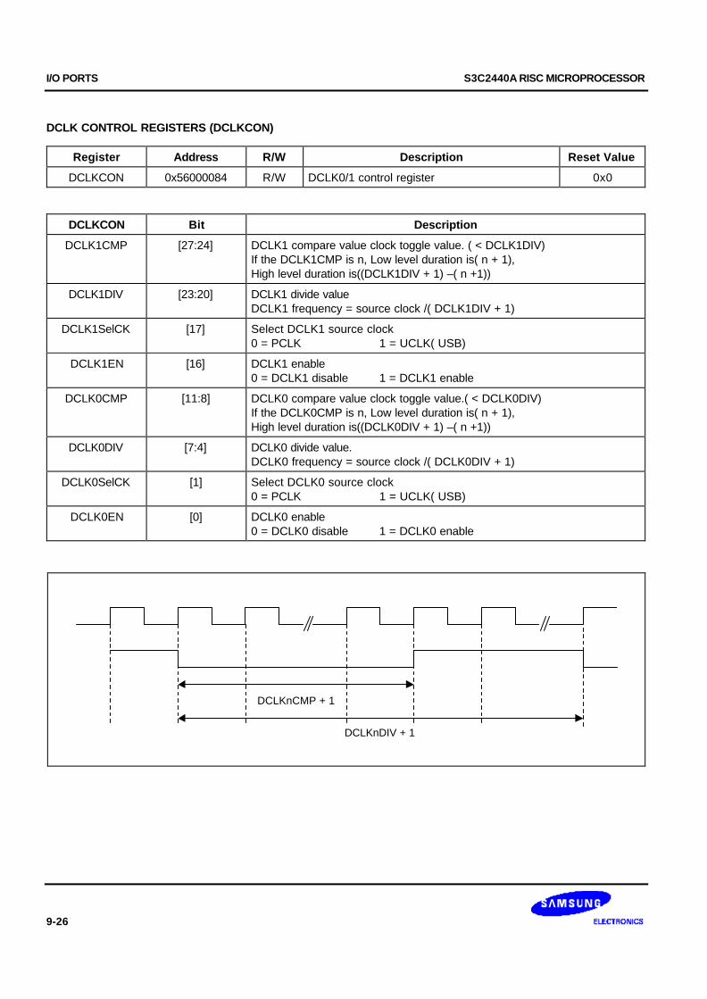
I/O PORTS S3C2440A RISC MICROPROCESSOR
9-26
DCLK CONTROL REGISTERS (DCLKCON)
Register Address R/W Description Reset Value
DCLKCON 0x56000084 R/W DCLK0/1 control register 0x0
DCLKCON Bit Description
DCLK1CMP [27:24] DCLK1 compare value clock toggle value. ( < DCLK1DIV)If the DCLK1CMP is n, Low level duration is( n + 1),High level duration is((DCLK1DIV + 1) –( n +1))
DCLK1DIV [23:20] DCLK1 divide valueDCLK1 frequency = source clock /( DCLK1DIV + 1)
DCLK1SelCK [17] Select DCLK1 source clock0 = PCLK 1 = UCLK( USB)
DCLK1EN [16] DCLK1 enable0 = DCLK1 disable 1 = DCLK1 enable
DCLK0CMP [11:8] DCLK0 compare value clock toggle value.( < DCLK0DIV)If the DCLK0CMP is n, Low level duration is( n + 1),High level duration is((DCLK0DIV + 1) –( n +1))
DCLK0DIV [7:4] DCLK0 divide value.DCLK0 frequency = source clock /( DCLK0DIV + 1)
DCLK0SelCK [1] Select DCLK0 source clock0 = PCLK 1 = UCLK( USB)
DCLK0EN [0] DCLK0 enable0 = DCLK0 disable 1 = DCLK0 enable
DCLKnDIV + 1
DCLKnCMP + 1

S3C2440A RISC MICROPROCESSOR I/O PORTS
9-27
EXTINTn (External Interrupt Control Register n)
The 8 external interrupts can be requested by various signaling methods. The EXTINT register configures thesignaling method between the level trigger and edge trigger for the external interrupt request, and also configures thesignal polarity.
To recognize the level interrupt, the valid logic level on EXTINTn pin must be retained for 40ns at least because of thenoise filter.
Register Address R/W Description Reset Value
EXTINT0 0x56000088 R/W External interrupt control register 0 0x000000
EXTINT1 0x5600008c R/W External interrupt control register 1 0x000000
EXTINT2 0x56000090 R/W External interrupt control register 2 0x000000
EXTINT0 Bit Description
EINT7 [30:28] Setting the signaling method of the EINT7.000 = Low level 001 = High level 01x = Falling edge triggered10x = Rising edge triggered 11x = Both edge triggered
EINT6 [26:24] Setting the signaling method of the EINT6.000 = Low level 001 = High level 01x = Falling edge triggered10x = Rising edge triggered 11x = Both edge triggered
EINT5 [22:20] Setting the signaling method of the EINT5.000 = Low level 001 = High level 01x = Falling edge triggered10x = Rising edge triggered 11x = Both edge triggered
EINT4 [18:16] Setting the signaling method of the EINT4.000 = Low level 001 = High level 01x = Falling edge triggered10x = Rising edge triggered 11x = Both edge triggered
EINT3 [14:12] Setting the signaling method of the EINT3.000 = Low level 001 = High level 01x = Falling edge triggered10x = Rising edge triggered 11x = Both edge triggered
EINT2 [10:8] Setting the signaling method of the EINT2.000 = Low level 001 = High level 01x = Falling edge triggered10x = Rising edge triggered 11x = Both edge triggered
EINT1 [6:4] Setting the signaling method of the EINT1.000 = Low level 001 = High level 01x = Falling edge triggered10x = Rising edge triggered 11x = Both edge triggered
EINT0 [2:0] Setting the signaling method of the EINT0.000 = Low level 001 = High level 01x = Falling edge triggered10x = Rising edge triggered 11x = Both edge triggered
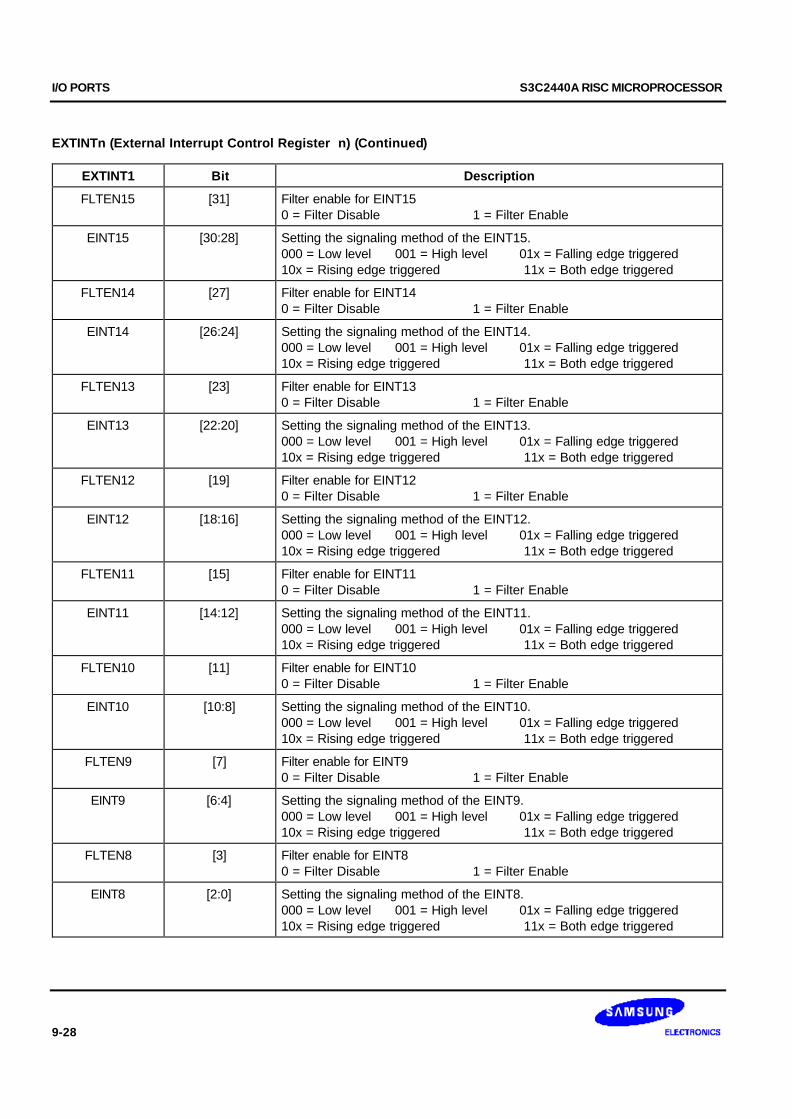
I/O PORTS S3C2440A RISC MICROPROCESSOR
9-28
EXTINTn (External Interrupt Control Register n) (Continued)
EXTINT1 Bit Description
FLTEN15 [31] Filter enable for EINT150 = Filter Disable 1 = Filter Enable
EINT15 [30:28] Setting the signaling method of the EINT15.000 = Low level 001 = High level 01x = Falling edge triggered10x = Rising edge triggered 11x = Both edge triggered
FLTEN14 [27] Filter enable for EINT140 = Filter Disable 1 = Filter Enable
EINT14 [26:24] Setting the signaling method of the EINT14.000 = Low level 001 = High level 01x = Falling edge triggered10x = Rising edge triggered 11x = Both edge triggered
FLTEN13 [23] Filter enable for EINT130 = Filter Disable 1 = Filter Enable
EINT13 [22:20] Setting the signaling method of the EINT13.000 = Low level 001 = High level 01x = Falling edge triggered10x = Rising edge triggered 11x = Both edge triggered
FLTEN12 [19] Filter enable for EINT120 = Filter Disable 1 = Filter Enable
EINT12 [18:16] Setting the signaling method of the EINT12.000 = Low level 001 = High level 01x = Falling edge triggered10x = Rising edge triggered 11x = Both edge triggered
FLTEN11 [15] Filter enable for EINT110 = Filter Disable 1 = Filter Enable
EINT11 [14:12] Setting the signaling method of the EINT11.000 = Low level 001 = High level 01x = Falling edge triggered10x = Rising edge triggered 11x = Both edge triggered
FLTEN10 [11] Filter enable for EINT100 = Filter Disable 1 = Filter Enable
EINT10 [10:8] Setting the signaling method of the EINT10.000 = Low level 001 = High level 01x = Falling edge triggered10x = Rising edge triggered 11x = Both edge triggered
FLTEN9 [7] Filter enable for EINT90 = Filter Disable 1 = Filter Enable
EINT9 [6:4] Setting the signaling method of the EINT9.000 = Low level 001 = High level 01x = Falling edge triggered10x = Rising edge triggered 11x = Both edge triggered
FLTEN8 [3] Filter enable for EINT80 = Filter Disable 1 = Filter Enable
EINT8 [2:0] Setting the signaling method of the EINT8.000 = Low level 001 = High level 01x = Falling edge triggered10x = Rising edge triggered 11x = Both edge triggered
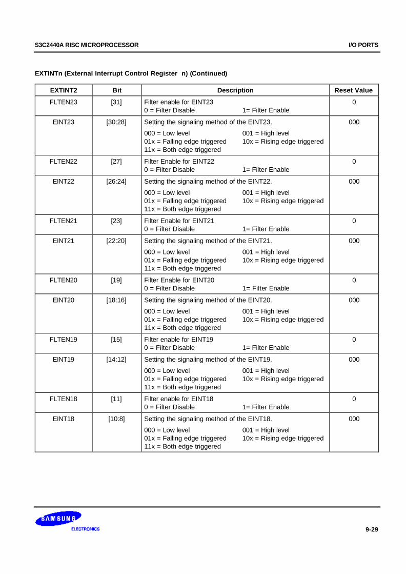
S3C2440A RISC MICROPROCESSOR I/O PORTS
9-29
EXTINTn (External Interrupt Control Register n) (Continued)
EXTINT2 Bit Description Reset Value
FLTEN23 [31] Filter enable for EINT230 = Filter Disable 1= Filter Enable
0
EINT23 [30:28] Setting the signaling method of the EINT23.
000 = Low level 001 = High level01x = Falling edge triggered 10x = Rising edge triggered11x = Both edge triggered
000
FLTEN22 [27] Filter Enable for EINT220 = Filter Disable 1= Filter Enable
0
EINT22 [26:24] Setting the signaling method of the EINT22.
000 = Low level 001 = High level01x = Falling edge triggered 10x = Rising edge triggered11x = Both edge triggered
000
FLTEN21 [23] Filter Enable for EINT210 = Filter Disable 1= Filter Enable
0
EINT21 [22:20] Setting the signaling method of the EINT21.
000 = Low level 001 = High level01x = Falling edge triggered 10x = Rising edge triggered11x = Both edge triggered
000
FLTEN20 [19] Filter Enable for EINT200 = Filter Disable 1= Filter Enable
0
EINT20 [18:16] Setting the signaling method of the EINT20.
000 = Low level 001 = High level01x = Falling edge triggered 10x = Rising edge triggered11x = Both edge triggered
000
FLTEN19 [15] Filter enable for EINT190 = Filter Disable 1= Filter Enable
0
EINT19 [14:12] Setting the signaling method of the EINT19.
000 = Low level 001 = High level01x = Falling edge triggered 10x = Rising edge triggered11x = Both edge triggered
000
FLTEN18 [11] Filter enable for EINT180 = Filter Disable 1= Filter Enable
0
EINT18 [10:8] Setting the signaling method of the EINT18.
000 = Low level 001 = High level01x = Falling edge triggered 10x = Rising edge triggered11x = Both edge triggered
000
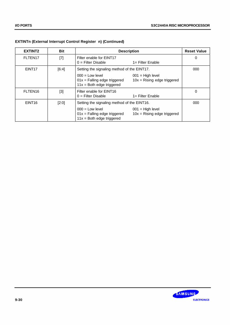
I/O PORTS S3C2440A RISC MICROPROCESSOR
9-30
EXTINTn (External Interrupt Control Register n) (Continued)
EXTINT2 Bit Description Reset Value
FLTEN17 [7] Filter enable for EINT170 = Filter Disable 1= Filter Enable
0
EINT17 [6:4] Setting the signaling method of the EINT17.
000 = Low level 001 = High level01x = Falling edge triggered 10x = Rising edge triggered11x = Both edge triggered
000
FLTEN16 [3] Filter enable for EINT160 = Filter Disable 1= Filter Enable
0
EINT16 [2:0] Setting the signaling method of the EINT16.
000 = Low level 001 = High level01x = Falling edge triggered 10x = Rising edge triggered11x = Both edge triggered
000
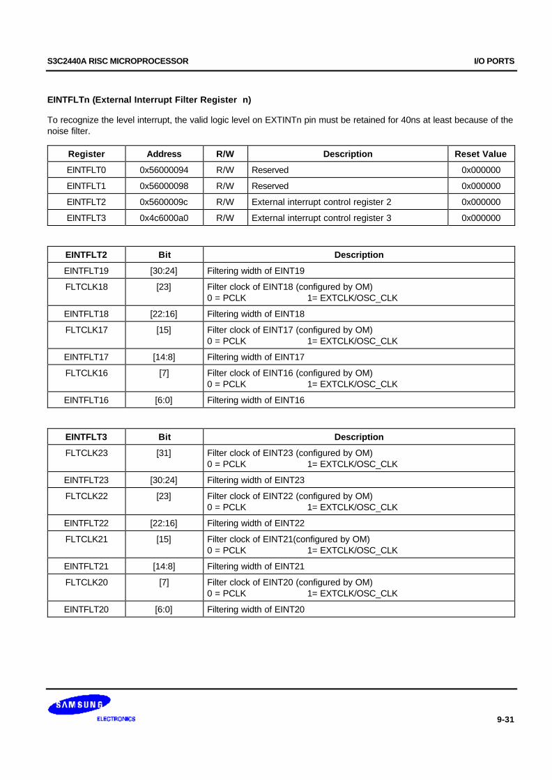
S3C2440A RISC MICROPROCESSOR I/O PORTS
9-31
EINTFLTn (External Interrupt Filter Register n)
To recognize the level interrupt, the valid logic level on EXTINTn pin must be retained for 40ns at least because of thenoise filter.
Register Address R/W Description Reset Value
EINTFLT0 0x56000094 R/W Reserved 0x000000
EINTFLT1 0x56000098 R/W Reserved 0x000000
EINTFLT2 0x5600009c R/W External interrupt control register 2 0x000000
EINTFLT3 0x4c6000a0 R/W External interrupt control register 3 0x000000
EINTFLT2 Bit Description
EINTFLT19 [30:24] Filtering width of EINT19
FLTCLK18 [23] Filter clock of EINT18 (configured by OM)0 = PCLK 1= EXTCLK/OSC_CLK
EINTFLT18 [22:16] Filtering width of EINT18
FLTCLK17 [15] Filter clock of EINT17 (configured by OM)0 = PCLK 1= EXTCLK/OSC_CLK
EINTFLT17 [14:8] Filtering width of EINT17
FLTCLK16 [7] Filter clock of EINT16 (configured by OM)0 = PCLK 1= EXTCLK/OSC_CLK
EINTFLT16 [6:0] Filtering width of EINT16
EINTFLT3 Bit Description
FLTCLK23 [31] Filter clock of EINT23 (configured by OM)0 = PCLK 1= EXTCLK/OSC_CLK
EINTFLT23 [30:24] Filtering width of EINT23
FLTCLK22 [23] Filter clock of EINT22 (configured by OM)0 = PCLK 1= EXTCLK/OSC_CLK
EINTFLT22 [22:16] Filtering width of EINT22
FLTCLK21 [15] Filter clock of EINT21(configured by OM)0 = PCLK 1= EXTCLK/OSC_CLK
EINTFLT21 [14:8] Filtering width of EINT21
FLTCLK20 [7] Filter clock of EINT20 (configured by OM)0 = PCLK 1= EXTCLK/OSC_CLK
EINTFLT20 [6:0] Filtering width of EINT20
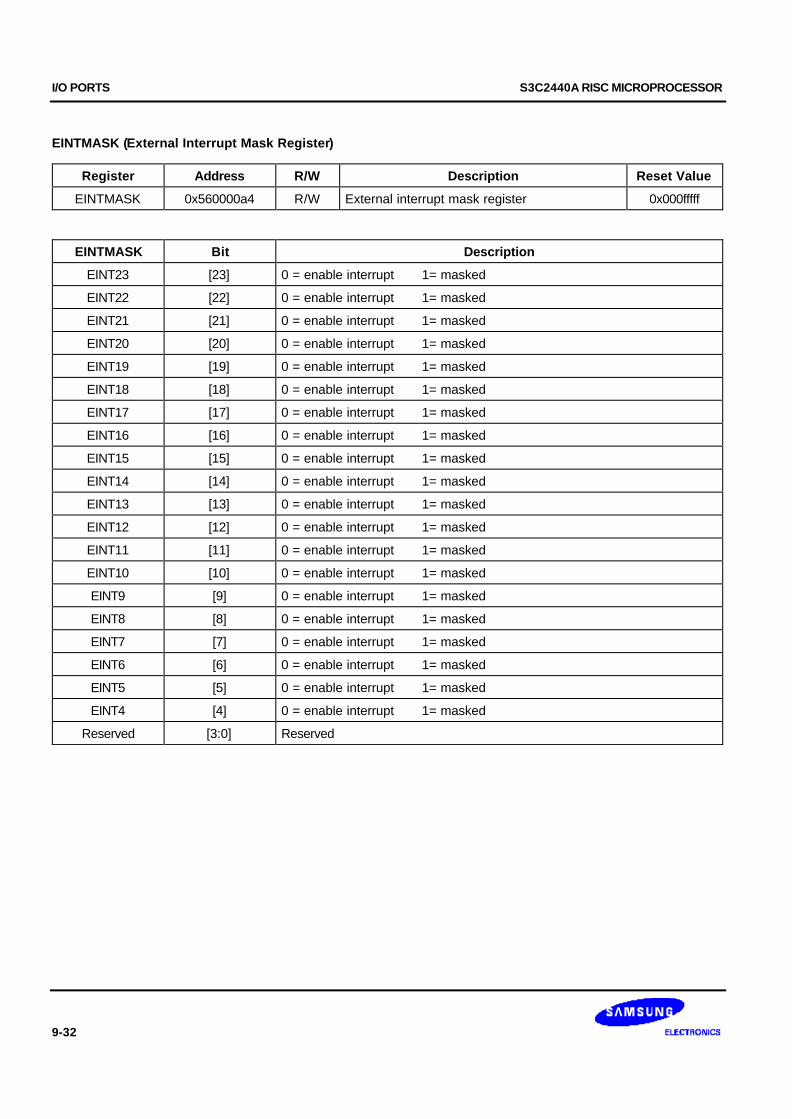
I/O PORTS S3C2440A RISC MICROPROCESSOR
9-32
EINTMASK (External Interrupt Mask Register)
Register Address R/W Description Reset Value
EINTMASK 0x560000a4 R/W External interrupt mask register 0x000fffff
EINTMASK Bit Description
EINT23 [23] 0 = enable interrupt 1= masked
EINT22 [22] 0 = enable interrupt 1= masked
EINT21 [21] 0 = enable interrupt 1= masked
EINT20 [20] 0 = enable interrupt 1= masked
EINT19 [19] 0 = enable interrupt 1= masked
EINT18 [18] 0 = enable interrupt 1= masked
EINT17 [17] 0 = enable interrupt 1= masked
EINT16 [16] 0 = enable interrupt 1= masked
EINT15 [15] 0 = enable interrupt 1= masked
EINT14 [14] 0 = enable interrupt 1= masked
EINT13 [13] 0 = enable interrupt 1= masked
EINT12 [12] 0 = enable interrupt 1= masked
EINT11 [11] 0 = enable interrupt 1= masked
EINT10 [10] 0 = enable interrupt 1= masked
EINT9 [9] 0 = enable interrupt 1= masked
EINT8 [8] 0 = enable interrupt 1= masked
EINT7 [7] 0 = enable interrupt 1= masked
EINT6 [6] 0 = enable interrupt 1= masked
EINT5 [5] 0 = enable interrupt 1= masked
EINT4 [4] 0 = enable interrupt 1= masked
Reserved [3:0] Reserved
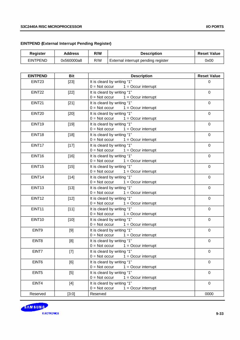
S3C2440A RISC MICROPROCESSOR I/O PORTS
9-33
EINTPEND (External Interrupt Pending Register)
Register Address R/W Description Reset Value
EINTPEND 0x560000a8 R/W External interrupt pending register 0x00
EINTPEND Bit Description Reset ValueEINT23 [23] It is cleard by writing “1”
0 = Not occur 1 = Occur interrupt0
EINT22 [22] It is cleard by writing “1”0 = Not occur 1 = Occur interrupt
0
EINT21 [21] It is cleard by writing “1”0 = Not occur 1 = Occur interrupt
0
EINT20 [20] It is cleard by writing “1”0 = Not occur 1 = Occur interrupt
0
EINT19 [19] It is cleard by writing “1”0 = Not occur 1 = Occur interrupt
0
EINT18 [18] It is cleard by writing “1”0 = Not occur 1 = Occur interrupt
0
EINT17 [17] It is cleard by writing “1”0 = Not occur 1 = Occur interrupt
0
EINT16 [16] It is cleard by writing “1”0 = Not occur 1 = Occur interrupt
0
EINT15 [15] It is cleard by writing “1”0 = Not occur 1 = Occur interrupt
0
EINT14 [14] It is cleard by writing “1”0 = Not occur 1 = Occur interrupt
0
EINT13 [13] It is cleard by writing “1”0 = Not occur 1 = Occur interrupt
0
EINT12 [12] It is cleard by writing “1”0 = Not occur 1 = Occur interrupt
0
EINT11 [11] It is cleard by writing “1”0 = Not occur 1 = Occur interrupt
0
EINT10 [10] It is cleard by writing “1”0 = Not occur 1 = Occur interrupt
0
EINT9 [9] It is cleard by writing “1”0 = Not occur 1 = Occur interrupt
0
EINT8 [8] It is cleard by writing “1”0 = Not occur 1 = Occur interrupt
0
EINT7 [7] It is cleard by writing “1”0 = Not occur 1 = Occur interrupt
0
EINT6 [6] It is cleard by writing “1”0 = Not occur 1 = Occur interrupt
0
EINT5 [5] It is cleard by writing “1”0 = Not occur 1 = Occur interrupt
0
EINT4 [4] It is cleard by writing “1”0 = Not occur 1 = Occur interrupt
0
Reserved [3:0] Reserved 0000

I/O PORTS S3C2440A RISC MICROPROCESSOR
9-34
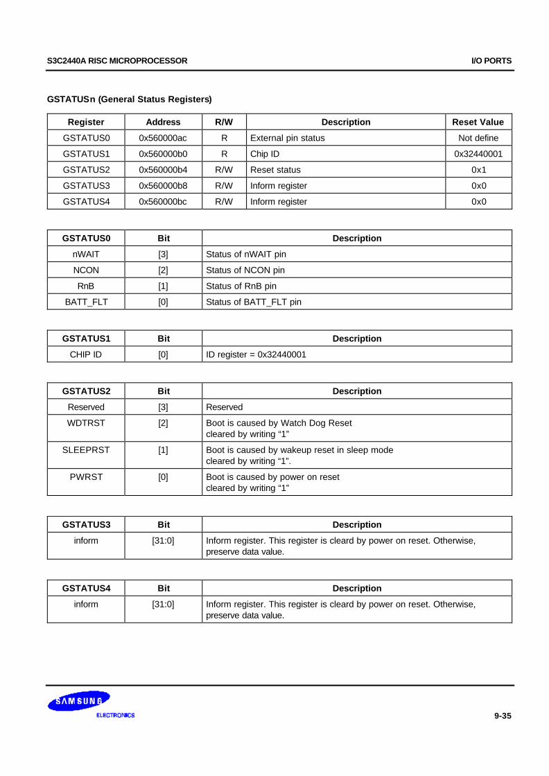
S3C2440A RISC MICROPROCESSOR I/O PORTS
9-35
GSTATUSn (General Status Registers)
Register Address R/W Description Reset Value
GSTATUS0 0x560000ac R External pin status Not define
GSTATUS1 0x560000b0 R Chip ID 0x32440001
GSTATUS2 0x560000b4 R/W Reset status 0x1
GSTATUS3 0x560000b8 R/W Inform register 0x0
GSTATUS4 0x560000bc R/W Inform register 0x0
GSTATUS0 Bit Description
nWAIT [3] Status of nWAIT pin
NCON [2] Status of NCON pin
RnB [1] Status of RnB pin
BATT_FLT [0] Status of BATT_FLT pin
GSTATUS1 Bit Description
CHIP ID [0] ID register = 0x32440001
GSTATUS2 Bit Description
Reserved [3] Reserved
WDTRST [2] Boot is caused by Watch Dog Resetcleared by writing “1”
SLEEPRST [1] Boot is caused by wakeup reset in sleep modecleared by writing “1”.
PWRST [0] Boot is caused by power on resetcleared by writing “1”
GSTATUS3 Bit Description
inform [31:0] Inform register. This register is cleard by power on reset. Otherwise,preserve data value.
GSTATUS4 Bit Description
inform [31:0] Inform register. This register is cleard by power on reset. Otherwise,preserve data value.

I/O PORTS S3C2440A RISC MICROPROCESSOR
9-36
DSCn (Drive Strength Control)
Control the Memory I/O drive strength
Register Address R/W Description Reset Value
DSC0 0x560000c4 R/W Strength control register 0 0x0
DSC1 0x560000c8 R/W Strength control register 1 0x0
DSC0 Bit Description Reset Value
nEN_DSC [31] Enable Drive Strength Control0: enable 1: Disable
0
Reserved [30:10] – 0
DSC_ADR [9:8] Address Bus Drive strength.00: 12mA 10: 10mA 01: 8mA 11: 6mA
00
DSC_DATA3 [7:6] DATA[31:24] I/O Drive strength.00: 12mA 10: 10mA 01: 8mA 11: 6mA
00
DSC_DATA2 [5:4] DATA[23:16] I/O Drive strength.00: 12mA 10: 10mA 01: 8mA 11: 6mA
00
DSC_DATA1 [3:2] DATA[15:8] I/O Drive strength.00: 12mA 10: 10mA 01: 8mA 11: 6mA
00
DSC_DATA0 [1:0] DATA[7:0] I/O Drive strength.00: 12mA 10: 10mA 01: 8mA 11: 6mA
00
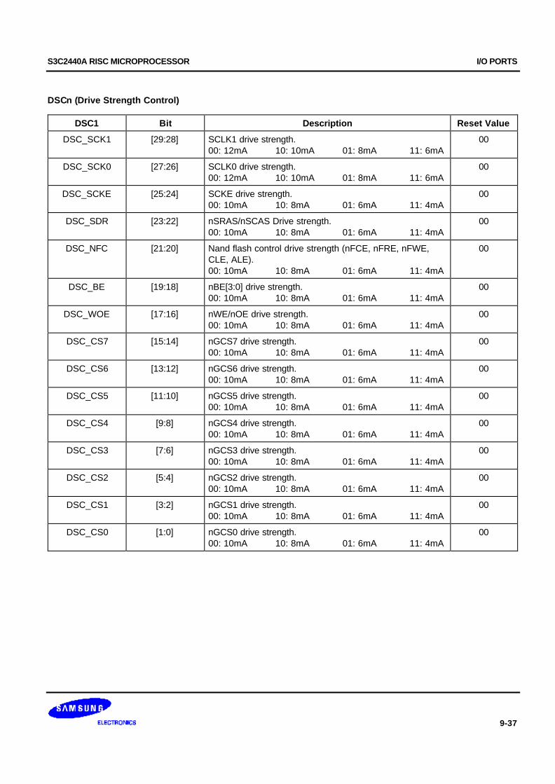
S3C2440A RISC MICROPROCESSOR I/O PORTS
9-37
DSCn (Drive Strength Control)
DSC1 Bit Description Reset Value
DSC_SCK1 [29:28] SCLK1 drive strength.00: 12mA 10: 10mA 01: 8mA 11: 6mA
00
DSC_SCK0 [27:26] SCLK0 drive strength.00: 12mA 10: 10mA 01: 8mA 11: 6mA
00
DSC_SCKE [25:24] SCKE drive strength.00: 10mA 10: 8mA 01: 6mA 11: 4mA
00
DSC_SDR [23:22] nSRAS/nSCAS Drive strength.00: 10mA 10: 8mA 01: 6mA 11: 4mA
00
DSC_NFC [21:20] Nand flash control drive strength (nFCE, nFRE, nFWE,CLE, ALE).00: 10mA 10: 8mA 01: 6mA 11: 4mA
00
DSC_BE [19:18] nBE[3:0] drive strength.00: 10mA 10: 8mA 01: 6mA 11: 4mA
00
DSC_WOE [17:16] nWE/nOE drive strength.00: 10mA 10: 8mA 01: 6mA 11: 4mA
00
DSC_CS7 [15:14] nGCS7 drive strength.00: 10mA 10: 8mA 01: 6mA 11: 4mA
00
DSC_CS6 [13:12] nGCS6 drive strength.00: 10mA 10: 8mA 01: 6mA 11: 4mA
00
DSC_CS5 [11:10] nGCS5 drive strength.00: 10mA 10: 8mA 01: 6mA 11: 4mA
00
DSC_CS4 [9:8] nGCS4 drive strength.00: 10mA 10: 8mA 01: 6mA 11: 4mA
00
DSC_CS3 [7:6] nGCS3 drive strength.00: 10mA 10: 8mA 01: 6mA 11: 4mA
00
DSC_CS2 [5:4] nGCS2 drive strength.00: 10mA 10: 8mA 01: 6mA 11: 4mA
00
DSC_CS1 [3:2] nGCS1 drive strength.00: 10mA 10: 8mA 01: 6mA 11: 4mA
00
DSC_CS0 [1:0] nGCS0 drive strength.00: 10mA 10: 8mA 01: 6mA 11: 4mA
00
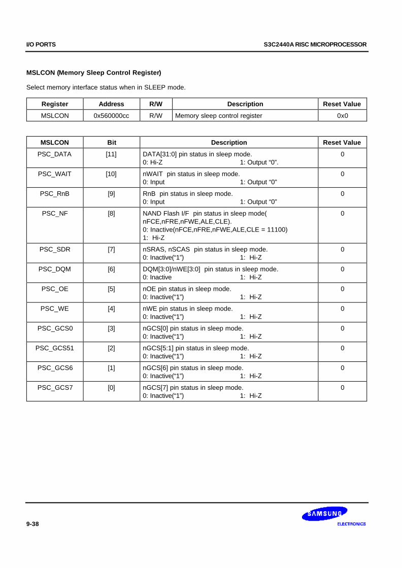
I/O PORTS S3C2440A RISC MICROPROCESSOR
9-38
MSLCON (Memory Sleep Control Register)
Select memory interface status when in SLEEP mode.
Register Address R/W Description Reset Value
MSLCON 0x560000cc R/W Memory sleep control register 0x0
MSLCON Bit Description Reset Value
PSC_DATA [11] DATA[31:0] pin status in sleep mode.0: Hi-Z 1: Output “0”.
0
PSC_WAIT [10] nWAIT pin status in sleep mode.0: Input 1: Output “0”
0
PSC_RnB [9] RnB pin status in sleep mode.0: Input 1: Output “0”
0
PSC_NF [8] NAND Flash I/F pin status in sleep mode(nFCE,nFRE,nFWE,ALE,CLE).0: Inactive(nFCE,nFRE,nFWE,ALE,CLE = 11100)1: Hi-Z
0
PSC_SDR [7] nSRAS, nSCAS pin status in sleep mode.0: Inactive(“1”) 1: Hi-Z
0
PSC_DQM [6] DQM[3:0]/nWE[3:0] pin status in sleep mode.0: Inactive 1: Hi-Z
0
PSC_OE [5] nOE pin status in sleep mode.0: Inactive(“1”) 1: Hi-Z
0
PSC_WE [4] nWE pin status in sleep mode.0: Inactive(“1”) 1: Hi-Z
0
PSC_GCS0 [3] nGCS[0] pin status in sleep mode.0: Inactive(“1”) 1: Hi-Z
0
PSC_GCS51 [2] nGCS[5:1] pin status in sleep mode.0: Inactive(“1”) 1: Hi-Z
0
PSC_GCS6 [1] nGCS[6] pin status in sleep mode.0: Inactive(“1”) 1: Hi-Z
0
PSC_GCS7 [0] nGCS[7] pin status in sleep mode.0: Inactive(“1”) 1: Hi-Z
0

S3C2440A RISC MICROPROCESSOR PWM TIMER
10-1
10 PWM TIMER
OVERVIEW
The S3C2440A has five 16-bit timers. Timer 0, 1, 2, and 3 have Pulse Width Modulation (PWM) function. Timer 4 hasan internal timer only with no output pins. The timer 0 has a dead-zone generator, which is used with a large currentdevice.
The timer 0 and 1 share an 8-bit prescaler, while the timer 2, 3 and 4 share other 8-bit prescaler. Each timer has aclock divider, which generates 5 different divided signals (1/2, 1/4, 1/8, 1/16, and TCLK). Each timer block receivesits own clock signals from the clock divider, which receives the clock from the corresponding 8-bit prescaler. The 8-bit prescaler is programmable and divides the PCLK according to the loading value, which is stored in TCFG0 andTCFG1 registers.
The timer count buffer register (TCNTBn) has an initial value which is loaded into the down-counter when the timer isenabled. The timer compare buffer register (TCMPBn) has an initial value which is loaded into the compare register tobe compared with the down-counter value. This double buffering feature of TCNTBn and TCMPBn makes the timergenerate a stable output when the frequency and duty ratio are changed.
Each timer has its own 16-bit down counter, which is driven by the timer clock. When the down counter reacheszero, the timer interrupt request is generated to inform the CPU that the timer operation has been completed. Whenthe timer counter reaches zero, the value of corresponding TCNTBn is automatically loaded into the down counter tocontinue the next operation. However, if the timer stops, for example, by clearing the timer enable bit of TCONnduring the timer running mode, the value of TCNTBn will not be reloaded into the counter.
The value of TCMPBn is used for pulse width modulation (PWM). The timer control logic changes the output levelwhen the down-counter value matches the value of the compare register in the timer control logic. Therefore, thecompare register determines the turn-on time (or turn-off time) of a PWM output.
FEATURE
— Five 16-bit timers
— Two 8-bit prescalers & Two 4-bit divider
— Programmable duty control of output waveform (PWM)
— Auto reload mode or one-shot pulse mode
— Dead-zone generator
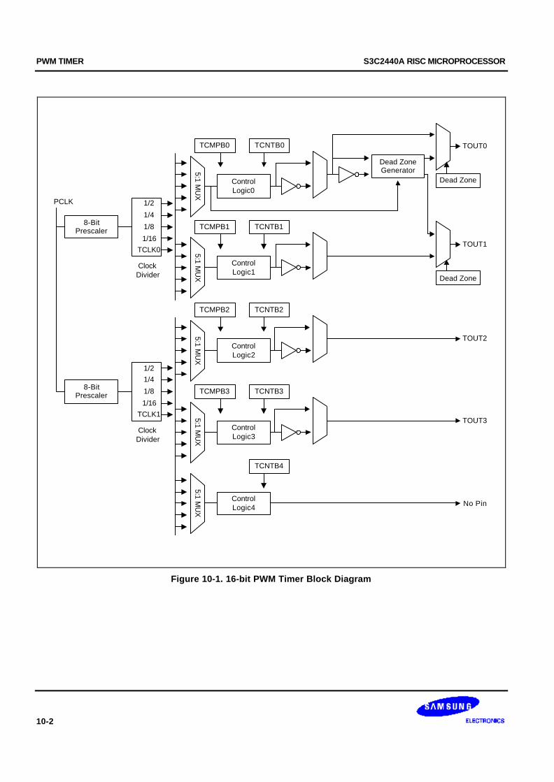
PWM TIMER S3C2440A RISC MICROPROCESSOR
10-2
ClockDivider
5:1 MU
X
Dead ZoneGenerator
TOUT0
TOUT1
TOUT2
ControlLogic0
TCMPB0 TCNTB0
ControlLogic1
TCMPB1 TCNTB1
5:1 MU
X
ClockDivider
5:1 MU
X5:1 M
UX
ControlLogic2
TCMPB2 TCNTB2
TOUT3ControlLogic3
TCMPB3 TCNTB3
No Pin
PCLK
8-BitPrescaler
8-BitPrescaler
Dead Zone
Dead Zone
TCLK0
1/8
1/4
1/16
1/2
TCLK1
1/8
1/4
1/16
1/2
5:1 MU
X
ControlLogic4
TCNTB4
Figure 10-1. 16-bit PWM Timer Block Diagram
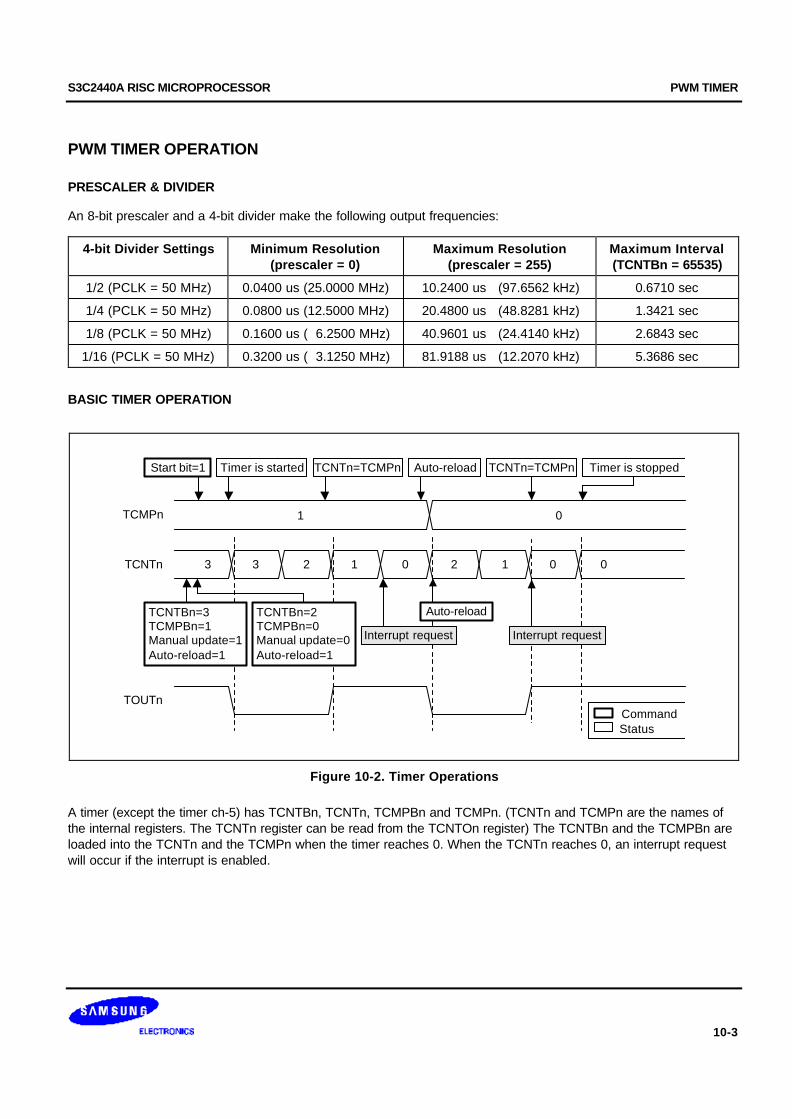
S3C2440A RISC MICROPROCESSOR PWM TIMER
10-3
PWM TIMER OPERATION
PRESCALER & DIVIDER
An 8-bit prescaler and a 4-bit divider make the following output frequencies:
4-bit Divider Settings Minimum Resolution(prescaler = 0)
Maximum Resolution(prescaler = 255)
Maximum Interval(TCNTBn = 65535)
1/2 (PCLK = 50 MHz) 0.0400 us (25.0000 MHz) 10.2400 us (97.6562 kHz) 0.6710 sec
1/4 (PCLK = 50 MHz) 0.0800 us (12.5000 MHz) 20.4800 us (48.8281 kHz) 1.3421 sec
1/8 (PCLK = 50 MHz) 0.1600 us ( 6.2500 MHz) 40.9601 us (24.4140 kHz) 2.6843 sec
1/16 (PCLK = 50 MHz) 0.3200 us ( 3.1250 MHz) 81.9188 us (12.2070 kHz) 5.3686 sec
BASIC TIMER OPERATION
TCMPn 1 0
TCNTn 3 3 2 1 0 2 1 0 0
Start bit=1 Timer is started TCNTn=TCMPn Auto-reload TCNTn=TCMPn Timer is stopped
TOUTnCommandStatus
TCNTBn=3TCMPBn=1Manual update=1Auto-reload=1
TCNTBn=2TCMPBn=0Manual update=0Auto-reload=1
Interrupt request
Auto-reload
Interrupt request
Figure 10-2. Timer Operations
A timer (except the timer ch-5) has TCNTBn, TCNTn, TCMPBn and TCMPn. (TCNTn and TCMPn are the names ofthe internal registers. The TCNTn register can be read from the TCNTOn register) The TCNTBn and the TCMPBn areloaded into the TCNTn and the TCMPn when the timer reaches 0. When the TCNTn reaches 0, an interrupt requestwill occur if the interrupt is enabled.
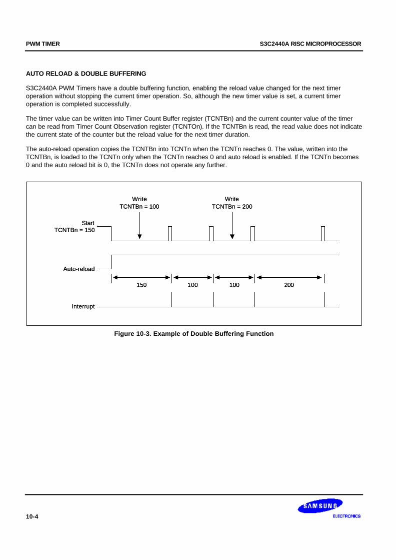
PWM TIMER S3C2440A RISC MICROPROCESSOR
10-4
AUTO RELOAD & DOUBLE BUFFERING
S3C2440A PWM Timers have a double buffering function, enabling the reload value changed for the next timeroperation without stopping the current timer operation. So, although the new timer value is set, a current timeroperation is completed successfully.
The timer value can be written into Timer Count Buffer register (TCNTBn) and the current counter value of the timercan be read from Timer Count Observation register (TCNTOn). If the TCNTBn is read, the read value does not indicatethe current state of the counter but the reload value for the next timer duration.
The auto-reload operation copies the TCNTBn into TCNTn when the TCNTn reaches 0. The value, written into theTCNTBn, is loaded to the TCNTn only when the TCNTn reaches 0 and auto reload is enabled. If the TCNTn becomes0 and the auto reload bit is 0, the TCNTn does not operate any further.
WriteTCNTBn = 100
WriteTCNTBn = 200
StartTCNTBn = 150
Auto-reload
150 100 100 200
Interrupt
WriteTCNTBn = 100
WriteTCNTBn = 200
StartTCNTBn = 150
Auto-reload
150 100 100 200
Interrupt
Figure 10-3. Example of Double Buffering Function
S3C2440A RISC MICROPROCESSOR PWM TIMER
10-5
TIMER INITIALIZATION USING MANUAL UPDATE BIT AND INVERTER BIT
An auto reload operation of the timer occurs when the down counter reaches 0. So, a starting value of the TCNTn hasto be defined by the user in advance. In this case, the starting value has to be loaded by the manual update bit. Thefollowing steps describe how to start a timer:
1) Write the initial value into TCNTBn and TCMPBn.
2) Set the manual update bit of the corresponding timer. It is recommended that you configure the inverter on/off bit.(Whether use inverter or not).
3) Set start bit of the corresponding timer to start the timer (and clear the manual update bit).
If the timer is stopped by force, the TCNTn retains the counter value and is not reloaded from TCNTBn. If a new valuehas to be set, perform manual update.
NOTE
Whenever TOUT inverter on/off bit is changed, the TOUTn logic value will also be changed whether the timerruns. Therefore, it is desirable that the inverter on/off bit is configured with the manual update bit.

PWM TIMER S3C2440A RISC MICROPROCESSOR
10-6
TIMER OPERATION
TOUTn
1 2 4 6
50 110 4040 6020
3 7 9 10
5 8 11
Figure 10-4. Example of a Timer Operation
The above Figure 10-4 shows the result of the following procedure:
1. Enable the auto re-load function. Set the TCNTBn to 160 (50+110) and the TCMPBn to 110. Set the manualupdate bit and configure the inverter bit (on/off). The manual update bit sets TCNTn and TCMPn to the values ofTCNTBn and TCMPBn, respectively.
And then, set the TCNTBn and the TCMPBn to 80 (40+40) and 40, respectively, to determine the next reloadvalue.
2. Set the start bit, provided that manual_update is 0 and the inverter is off and auto reload is on. The timer startscounting down after latency time within the timer resolution.
3. When the TCNTn has the same value as that of the TCMPn, the logic level of the TOUTn is changed from low tohigh.
4. When the TCNTn reaches 0, the interrupt request is generated and TCNTBn value is loaded into a temporaryregister. At the next timer tick, the TCNTn is reloaded with the temporary register value (TCNTBn).
5. In Interrupt Service Routine (ISR), the TCNTBn and the TCMPBn are set to 80 (20+60) and 60, respectively, forthe next duration.
6. When the TCNTn has the same value as the TCMPn, the logic level of TOUTn is changed from low to high.
7. When the TCNTn reaches 0, the TCNTn is reloaded automatically with the TCNTBn, triggering an interruptrequest.
8. In Interrupt Service Routine (ISR), auto reload and interrupt request are disabled to stop the timer.
9. When the value of the TCNTn is same as the TCMPn, the logic level of the TOUTn is changed from low to high.
10. Even when the TCNTn reaches 0, the TCNTn is not any more reloaded and the timer is stopped because autoreload has been disabled.
11. No more interrupt requests are generated.
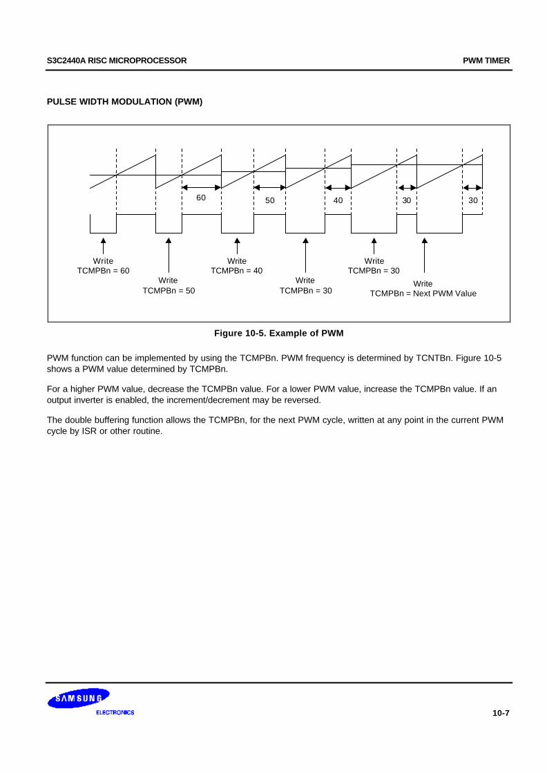
S3C2440A RISC MICROPROCESSOR PWM TIMER
10-7
PULSE WIDTH MODULATION (PWM)
WriteTCMPBn = 60
WriteTCMPBn = 50
WriteTCMPBn = 40
WriteTCMPBn = 30
WriteTCMPBn = 30
WriteTCMPBn = Next PWM Value
60 50 40 30 30
Figure 10-5. Example of PWM
PWM function can be implemented by using the TCMPBn. PWM frequency is determined by TCNTBn. Figure 10-5shows a PWM value determined by TCMPBn.
For a higher PWM value, decrease the TCMPBn value. For a lower PWM value, increase the TCMPBn value. If anoutput inverter is enabled, the increment/decrement may be reversed.
The double buffering function allows the TCMPBn, for the next PWM cycle, written at any point in the current PWMcycle by ISR or other routine.

PWM TIMER S3C2440A RISC MICROPROCESSOR
10-8
OUTPUT LEVEL CONTROL
Inverter off
Initial State Period 1 Period 2 Timer Stop
Inverter on
Figure 10-6. Inverter On/Off
The following procedure describes how to maintain TOUT as high or low (assume the inverter is off):
1. Turn off the auto reload bit. And then, TOUTn goes to high level and the timer is stopped after the TCNTn reaches0 (recommended).
2. Stop the timer by clearing the timer start/stop bit to 0. If TCNTn ¡ TCMPn, the output level is high. If TCNTn>TCMPn, the output level is low.
3. The TOUTn can be inverted by the inverter on/off bit in TCON. The inverter removes the additional circuit toadjust the output level.
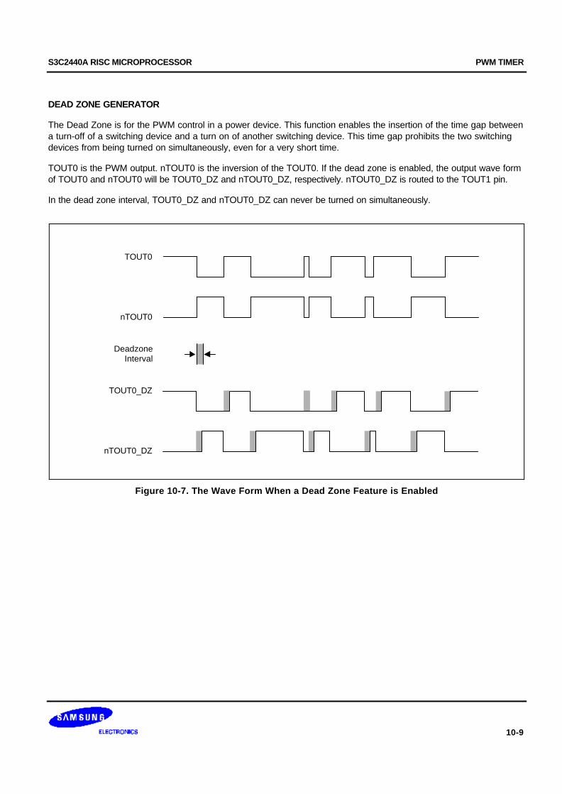
S3C2440A RISC MICROPROCESSOR PWM TIMER
10-9
DEAD ZONE GENERATOR
The Dead Zone is for the PWM control in a power device. This function enables the insertion of the time gap betweena turn-off of a switching device and a turn on of another switching device. This time gap prohibits the two switchingdevices from being turned on simultaneously, even for a very short time.
TOUT0 is the PWM output. nTOUT0 is the inversion of the TOUT0. If the dead zone is enabled, the output wave formof TOUT0 and nTOUT0 will be TOUT0_DZ and nTOUT0_DZ, respectively. nTOUT0_DZ is routed to the TOUT1 pin.
In the dead zone interval, TOUT0_DZ and nTOUT0_DZ can never be turned on simultaneously.
TOUT0
nTOUT0
TOUT0_DZ
nTOUT0_DZ
DeadzoneInterval
Figure 10-7. The Wave Form When a Dead Zone Feature is Enabled
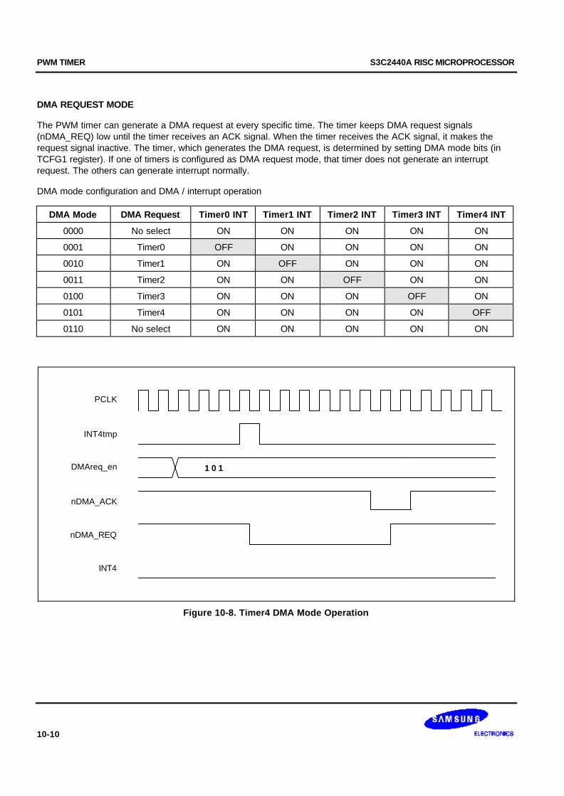
PWM TIMER S3C2440A RISC MICROPROCESSOR
10-10
DMA REQUEST MODE
The PWM timer can generate a DMA request at every specific time. The timer keeps DMA request signals(nDMA_REQ) low until the timer receives an ACK signal. When the timer receives the ACK signal, it makes therequest signal inactive. The timer, which generates the DMA request, is determined by setting DMA mode bits (inTCFG1 register). If one of timers is configured as DMA request mode, that timer does not generate an interruptrequest. The others can generate interrupt normally.
DMA mode configuration and DMA / interrupt operation
DMA Mode DMA Request Timer0 INT Timer1 INT Timer2 INT Timer3 INT Timer4 INT
0000 No select ON ON ON ON ON
0001 Timer0 OFF ON ON ON ON
0010 Timer1 ON OFF ON ON ON
0011 Timer2 ON ON OFF ON ON
0100 Timer3 ON ON ON OFF ON
0101 Timer4 ON ON ON ON OFF
0110 No select ON ON ON ON ON
PCLK
INT4tmp
DMAreq_en
nDMA_ACK
nDMA_REQ
INT4
1 0 1
Figure 10-8. Timer4 DMA Mode Operation
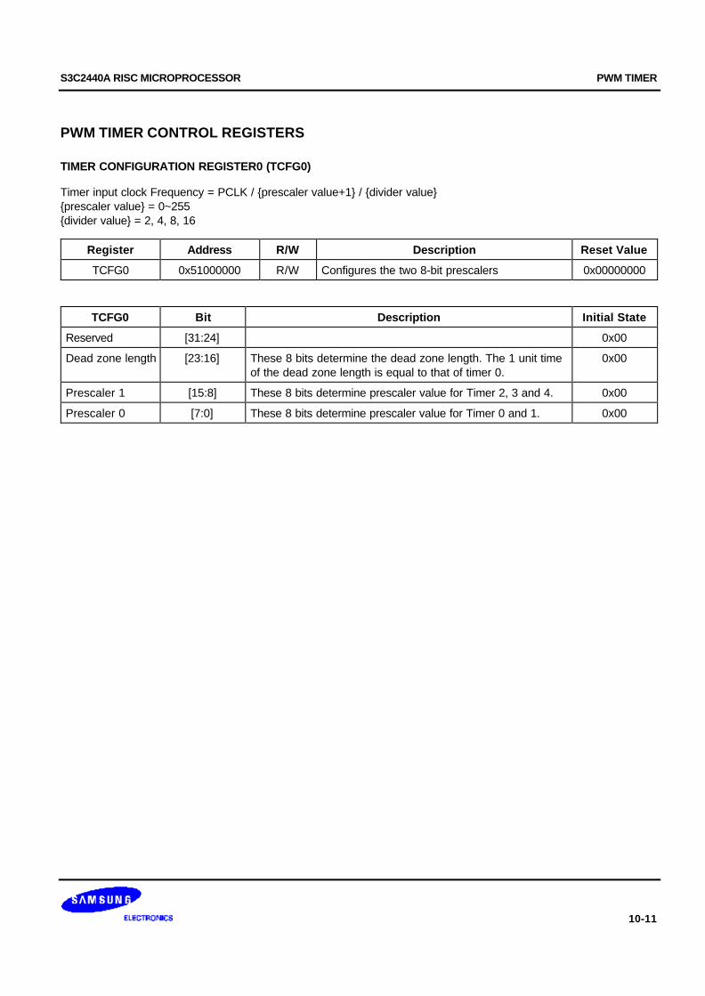
S3C2440A RISC MICROPROCESSOR PWM TIMER
10-11
PWM TIMER CONTROL REGISTERS
TIMER CONFIGURATION REGISTER0 (TCFG0)
Timer input clock Frequency = PCLK / prescaler value+1 / divider valueprescaler value = 0~255divider value = 2, 4, 8, 16
Register Address R/W Description Reset Value
TCFG0 0x51000000 R/W Configures the two 8-bit prescalers 0x00000000
TCFG0 Bit Description Initial State
Reserved [31:24] 0x00
Dead zone length [23:16] These 8 bits determine the dead zone length. The 1 unit timeof the dead zone length is equal to that of timer 0.
0x00
Prescaler 1 [15:8] These 8 bits determine prescaler value for Timer 2, 3 and 4. 0x00
Prescaler 0 [7:0] These 8 bits determine prescaler value for Timer 0 and 1. 0x00
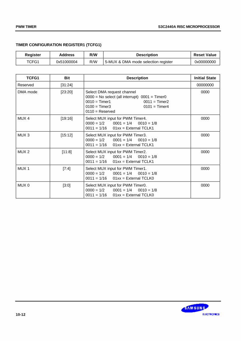
PWM TIMER S3C2440A RISC MICROPROCESSOR
10-12
TIMER CONFIGURATION REGISTER1 (TCFG1)
Register Address R/W Description Reset Value
TCFG1 0x51000004 R/W 5-MUX & DMA mode selection register 0x00000000
TCFG1 Bit Description Initial State
Reserved [31:24] 00000000
DMA mode [23:20] Select DMA request channel0000 = No select (all interrupt) 0001 = Timer00010 = Timer1 0011 = Timer20100 = Timer3 0101 = Timer40110 = Reserved
0000
MUX 4 [19:16] Select MUX input for PWM Timer4.0000 = 1/2 0001 = 1/4 0010 = 1/80011 = 1/16 01xx = External TCLK1
0000
MUX 3 [15:12] Select MUX input for PWM Timer3.0000 = 1/2 0001 = 1/4 0010 = 1/80011 = 1/16 01xx = External TCLK1
0000
MUX 2 [11:8] Select MUX input for PWM Timer2.0000 = 1/2 0001 = 1/4 0010 = 1/80011 = 1/16 01xx = External TCLK1
0000
MUX 1 [7:4] Select MUX input for PWM Timer1.0000 = 1/2 0001 = 1/4 0010 = 1/80011 = 1/16 01xx = External TCLK0
0000
MUX 0 [3:0] Select MUX input for PWM Timer0.0000 = 1/2 0001 = 1/4 0010 = 1/80011 = 1/16 01xx = External TCLK0
0000
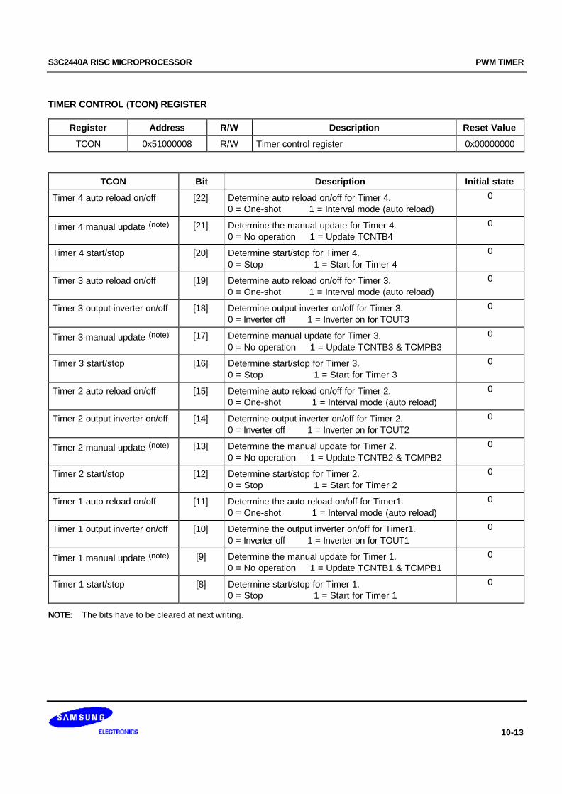
S3C2440A RISC MICROPROCESSOR PWM TIMER
10-13
TIMER CONTROL (TCON) REGISTER
Register Address R/W Description Reset Value
TCON 0x51000008 R/W Timer control register 0x00000000
TCON Bit Description Initial state
Timer 4 auto reload on/off [22] Determine auto reload on/off for Timer 4.0 = One-shot 1 = Interval mode (auto reload)
0
Timer 4 manual update (note) [21] Determine the manual update for Timer 4.0 = No operation 1 = Update TCNTB4
0
Timer 4 start/stop [20] Determine start/stop for Timer 4.0 = Stop 1 = Start for Timer 4
0
Timer 3 auto reload on/off [19] Determine auto reload on/off for Timer 3.0 = One-shot 1 = Interval mode (auto reload)
0
Timer 3 output inverter on/off [18] Determine output inverter on/off for Timer 3.0 = Inverter off 1 = Inverter on for TOUT3
0
Timer 3 manual update (note) [17] Determine manual update for Timer 3.0 = No operation 1 = Update TCNTB3 & TCMPB3
0
Timer 3 start/stop [16] Determine start/stop for Timer 3.0 = Stop 1 = Start for Timer 3
0
Timer 2 auto reload on/off [15] Determine auto reload on/off for Timer 2.0 = One-shot 1 = Interval mode (auto reload)
0
Timer 2 output inverter on/off [14] Determine output inverter on/off for Timer 2.0 = Inverter off 1 = Inverter on for TOUT2
0
Timer 2 manual update (note) [13] Determine the manual update for Timer 2.0 = No operation 1 = Update TCNTB2 & TCMPB2
0
Timer 2 start/stop [12] Determine start/stop for Timer 2.0 = Stop 1 = Start for Timer 2
0
Timer 1 auto reload on/off [11] Determine the auto reload on/off for Timer1.0 = One-shot 1 = Interval mode (auto reload)
0
Timer 1 output inverter on/off [10] Determine the output inverter on/off for Timer1.0 = Inverter off 1 = Inverter on for TOUT1
0
Timer 1 manual update (note) [9] Determine the manual update for Timer 1.0 = No operation 1 = Update TCNTB1 & TCMPB1
0
Timer 1 start/stop [8] Determine start/stop for Timer 1.0 = Stop 1 = Start for Timer 1
0
NOTE: The bits have to be cleared at next writing.
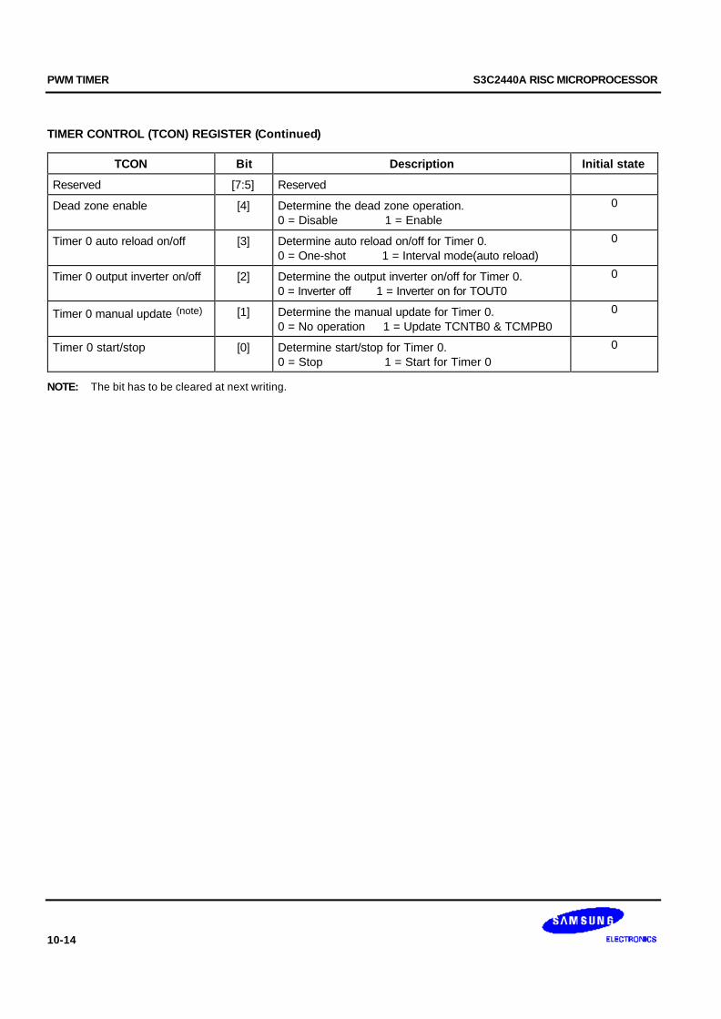
PWM TIMER S3C2440A RISC MICROPROCESSOR
10-14
TIMER CONTROL (TCON) REGISTER (Continued)
TCON Bit Description Initial state
Reserved [7:5] Reserved
Dead zone enable [4] Determine the dead zone operation.0 = Disable 1 = Enable
0
Timer 0 auto reload on/off [3] Determine auto reload on/off for Timer 0.0 = One-shot 1 = Interval mode(auto reload)
0
Timer 0 output inverter on/off [2] Determine the output inverter on/off for Timer 0.0 = Inverter off 1 = Inverter on for TOUT0
0
Timer 0 manual update (note) [1] Determine the manual update for Timer 0.0 = No operation 1 = Update TCNTB0 & TCMPB0
0
Timer 0 start/stop [0] Determine start/stop for Timer 0.0 = Stop 1 = Start for Timer 0
0
NOTE: The bit has to be cleared at next writing.
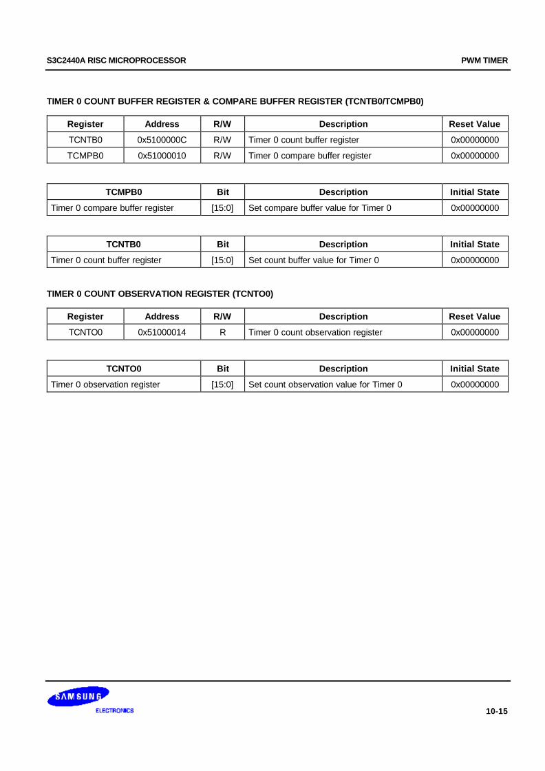
S3C2440A RISC MICROPROCESSOR PWM TIMER
10-15
TIMER 0 COUNT BUFFER REGISTER & COMPARE BUFFER REGISTER (TCNTB0/TCMPB0)
Register Address R/W Description Reset Value
TCNTB0 0x5100000C R/W Timer 0 count buffer register 0x00000000
TCMPB0 0x51000010 R/W Timer 0 compare buffer register 0x00000000
TCMPB0 Bit Description Initial State
Timer 0 compare buffer register [15:0] Set compare buffer value for Timer 0 0x00000000
TCNTB0 Bit Description Initial State
Timer 0 count buffer register [15:0] Set count buffer value for Timer 0 0x00000000
TIMER 0 COUNT OBSERVATION REGISTER (TCNTO0)
Register Address R/W Description Reset Value
TCNTO0 0x51000014 R Timer 0 count observation register 0x00000000
TCNTO0 Bit Description Initial State
Timer 0 observation register [15:0] Set count observation value for Timer 0 0x00000000
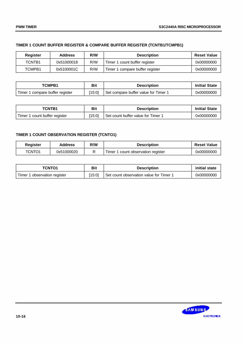
PWM TIMER S3C2440A RISC MICROPROCESSOR
10-16
TIMER 1 COUNT BUFFER REGISTER & COMPARE BUFFER REGISTER (TCNTB1/TCMPB1)
Register Address R/W Description Reset Value
TCNTB1 0x51000018 R/W Timer 1 count buffer register 0x00000000
TCMPB1 0x5100001C R/W Timer 1 compare buffer register 0x00000000
TCMPB1 Bit Description Initial State
Timer 1 compare buffer register [15:0] Set compare buffer value for Timer 1 0x00000000
TCNTB1 Bit Description Initial State
Timer 1 count buffer register [15:0] Set count buffer value for Timer 1 0x00000000
TIMER 1 COUNT OBSERVATION REGISTER (TCNTO1)
Register Address R/W Description Reset Value
TCNTO1 0x51000020 R Timer 1 count observation register 0x00000000
TCNTO1 Bit Description initial state
Timer 1 observation register [15:0] Set count observation value for Timer 1 0x00000000
S3C2440A RISC MICROPROCESSOR PWM TIMER
10-17
TIMER 2 COUNT BUFFER REGISTER & COMPARE BUFFER REGISTER (TCNTB2/TCMPB2)
Register Address R/W Description Reset Value
TCNTB2 0x51000024 R/W Timer 2 count buffer register 0x00000000
TCMPB2 0x51000028 R/W Timer 2 compare buffer register 0x00000000
TCMPB2 Bit Description Initial State
Timer 2 compare buffer register [15:0] Set compare buffer value for Timer 2 0x00000000
TCNTB2 Bit Description Initial State
Timer 2 count buffer register [15:0] Set count buffer value for Timer 2 0x00000000
TIMER 2 COUNT OBSERVATION REGISTER (TCNTO2)
Register Address R/W Description Reset Value
TCNTO2 0x5100002C R Timer 2 count observation register 0x00000000
TCNTO2 Bit Description Initial State
Timer 2 observation register [15:0] Set count observation value for Timer 2 0x00000000
PWM TIMER S3C2440A RISC MICROPROCESSOR
10-18
TIMER 3 COUNT BUFFER REGISTER & COMPARE BUFFER REGISTER (TCNTB3/TCMPB3)
Register Address R/W Description Reset Value
TCNTB3 0x51000030 R/W Timer 3 count buffer register 0x00000000
TCMPB3 0x51000034 R/W Timer 3 compare buffer register 0x00000000
TCMPB3 Bit Description Initial State
Timer 3 compare buffer register [15:0] Set compare buffer value for Timer 3 0x00000000
TCNTB3 Bit Description Initial State
Timer 3 count buffer register [15:0] Set count buffer value for Timer 3 0x00000000
TIMER 3 COUNT OBSERVATION REGISTER (TCNTO3)
Register Address R/W Description Reset Value
TCNTO3 0x51000038 R Timer 3 count observation register 0x00000000
TCNTO3 Bit Description Initial State
Timer 3 observation register [15:0] Set count observation value for Timer 3 0x00000000

S3C2440A RISC MICROPROCESSOR PWM TIMER
10-19
TIMER 4 COUNT BUFFER REGISTER (TCNTB4)
Register Address R/W Description Reset Value
TCNTB4 0x5100003C R/W Timer 4 count buffer register 0x00000000
TCNTB4 Bit Description Initial State
Timer 4 count buffer register [15:0] Set count buffer value for Timer 4 0x00000000
TIMER 4 COUNT OBSERVATION REGISTER (TCNTO4)
Register Address R/W Description Reset Value
TCNTO4 0x51000040 R Timer 4 count observation register 0x00000000
TCNTO4 Bit Description Initial State
Timer 4 observation register [15:0] Set count observation value for Timer 4 0x00000000

PWM TIMER S3C2440A RISC MICROPROCESSOR
10-20
NOTES
S3C2440A RISC MICROPROCESSOR UART
11-1
11 UART
OVERVIEW
The S3C2440A Universal Asynchronous Receiver and Transmitter (UART) provide three independent asynchronousserial I/O (SIO) ports, each of which can operate in Interrupt-based or DMA-based mode. In other words, the UARTcan generate an interrupt or a DMA request to transfer data between CPU and the UART. The UART can support bitrates up to 115.2K bps using system clock. If an external device provides the UART with UEXTCLK, then the UARTcan operate at higher speed. Each UART channel contains two 64-byte FIFOs for receiver and transmitter.
The S3C2440A UART includes programmable baud rates, infrared (IR) transmit/receive, one or two stop bit insertion,5-bit, 6-bit, 7-bit or 8-bit data width and parity checking.
Each UART contains a baud-rate generator, transmitter, receiver and a control unit, as shown in Figure 11-1. Thebaud-rate generator can be clocked by PCLK, FCLK/n or UEXTCLK (external input clock). The transmitter and thereceiver contain 64-byte FIFOs and data shifters. Data is written to FIFO and then copied to the transmit shifterbefore being transmitted. The data is then shifted out by the transmit data pin (TxDn). Meanwhile, received data isshifted from the receive data pin (RxDn), and then copied to FIFO from the shifter.
FEATURES
— RxD0, TxD0, RxD1, TxD1, RxD2, and TxD2 with DMA-based or interrupt-based operation
— UART Ch 0, 1, and 2 with IrDA 1.0 & 64-byte FIFO
— UART Ch 0 and 1 with nRTS0, nCTS0, nRTS1, and nCTS1
— Supports handshake transmit/receive
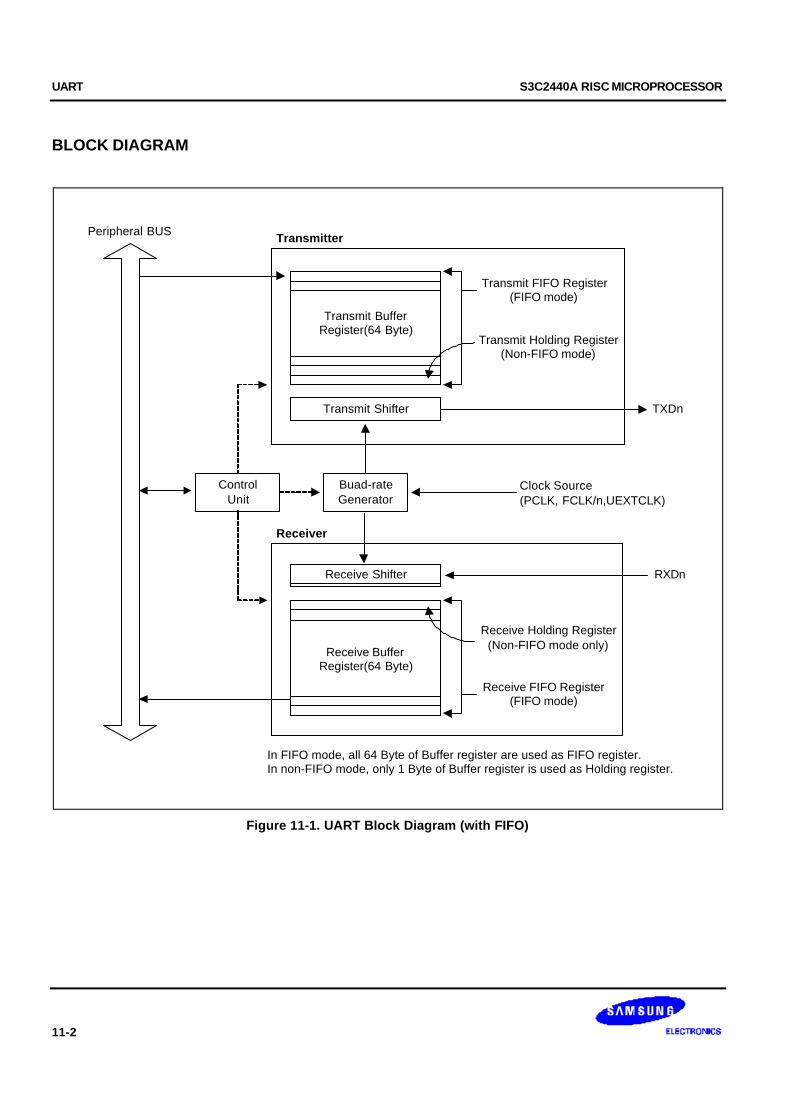
UART S3C2440A RISC MICROPROCESSOR
11-2
BLOCK DIAGRAM
Buad-rateGenerator
ControlUnit
Transmitter
Receiver
Peripheral BUS
TXDn
Clock Source(PCLK, FCLK/n,UEXTCLK)
RXDn
Transmit FIFO Register(FIFO mode)
Transmit Holding Register(Non-FIFO mode)
Receive FIFO Register(FIFO mode)
Receive Holding Register(Non-FIFO mode only)
In FIFO mode, all 64 Byte of Buffer register are used as FIFO register.In non-FIFO mode, only 1 Byte of Buffer register is used as Holding register.
Transmit Shifter
Transmit BufferRegister(64 Byte)
Receive Shifter
Receive BufferRegister(64 Byte)
Figure 11-1. UART Block Diagram (with FIFO)
S3C2440A RISC MICROPROCESSOR UART
11-3
UART OPERATION
The following sections describe the UART operations that include data transmission, data reception, interruptgeneration, baud-rate generation, Loopback mode, Infrared mode, and auto flow control.
Data Transmission
The data frame for transmission is programmable. It consists of a start bit, 5 to 8 data bits, an optional parity bit and1 to 2 stop bits, which can be specified by the line control register (ULCONn). The transmitter can also produce thebreak condition, which forces the serial output to logic 0 state for one frame transmission time. This block transmitsbreak signals after the present transmission word is transmitted completely. After the break signal transmission, itcontinuously transmits data into the Tx FIFO (Tx holding register in the case of Non-FIFO mode).
Data Reception
Like the transmission, the data frame for reception is also programmable. It consists of a start bit, 5 to 8 data bits,an optional parity bit and 1 to 2 stop bits in the line control register (ULCONn). The receiver can detect overrun error,parity error, frame error and break condition, each of which can set an error flag.
— The overrun error indicates that new data has overwritten the old data before the old data has been read.
— The parity error indicates that the receiver has detected an unexpected parity condition.
— The frame error indicates that the received data does not have a valid stop bit.
— The break condition indicates that the RxDn input is held in the logic 0 state for a duration longer than one frame transmission time.
Receive time-out condition occurs when it does not receive any data during the 3 word time (this interval follows thesetting of Word Length bit) and the Rx FIFO is not empty in the FIFO mode.
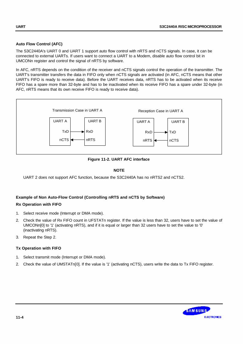
UART S3C2440A RISC MICROPROCESSOR
11-4
Auto Flow Control (AFC)
The S3C2440A's UART 0 and UART 1 support auto flow control with nRTS and nCTS signals. In case, it can beconnected to external UARTs. If users want to connect a UART to a Modem, disable auto flow control bit inUMCONn register and control the signal of nRTS by software.
In AFC, nRTS depends on the condition of the receiver and nCTS signals control the operation of the transmitter. TheUART's transmitter transfers the data in FIFO only when nCTS signals are activated (in AFC, nCTS means that otherUART's FIFO is ready to receive data). Before the UART receives data, nRTS has to be activated when its receiveFIFO has a spare more than 32-byte and has to be inactivated when its receive FIFO has a spare under 32-byte (inAFC, nRTS means that its own receive FIFO is ready to receive data).
UART A
TxD
nCTS
UART B
RxD
nRTS
Transmission Case in UART A
UART A
RxD
nRTS
UART B
TxD
nCTS
Reception Case in UART A
Figure 11-2. UART AFC interface
NOTE
UART 2 does not support AFC function, because the S3C2440A has no nRTS2 and nCTS2.
Example of Non Auto-Flow Control (Controlling nRTS and nCTS by Software)
Rx Operation with FIFO
1. Select receive mode (Interrupt or DMA mode).
2. Check the value of Rx FIFO count in UFSTATn register. If the value is less than 32, users have to set the value ofUMCONn[0] to '1' (activating nRTS), and if it is equal or larger than 32 users have to set the value to '0'(inactivating nRTS).
3. Repeat the Step 2.
Tx Operation with FIFO
1. Select transmit mode (Interrupt or DMA mode).
2. Check the value of UMSTATn[0]. If the value is '1' (activating nCTS), users write the data to Tx FIFO register.
S3C2440A RISC MICROPROCESSOR UART
11-5
RS-232C interface
If the user wants to connect the UART to modem interface (instead of null modem), nRTS, nCTS, nDSR, nDTR, DCDand nRI signals are needed. In this case, the users can control these signals with general I/O ports by softwarebecause the AFC does not support the RS-232C interface.
Interrupt/DMA Request Generation
Each UART of the S3C2440A has seven status (Tx/Rx/Error) signals: Overrun error, Parity error, Frame error, Break,Receive buffer data ready, Transmit buffer empty, and Transmit shifter empty, all of which are indicated by thecorresponding UART status register (UTRSTATn/UERSTATn).
The overrun error, parity error, frame error and break condition are referred to as the receive error status. Each ofwhich can cause the receive error status interrupt request, if the receive-error-status-interrupt-enable bit is set to onein the control register, UCONn. When a receive-error-status-interrupt-request is detected, the signal causing therequest can be identified by reading the value of UERSTSTn.
When the receiver transfers the data of the receive shifter to the receive FIFO register in FIFO mode and the numberof received data reaches Rx FIFO Trigger Level, Rx interrupt is generated. If the Receive mode is in control register(UCONn) and is selected as 1 (Interrupt request or polling mode). In the Non-FIFO mode, transferring the data of thereceive shifter to receive holding register will cause Rx interrupt under the Interrupt request and polling mode.
When the transmitter transfers data from its transmit FIFO register to its transmit shifter and the number of data leftin transmit FIFO reaches Tx FIFO Trigger Level, Tx interrupt is generated, if Transmit mode in control register isselected as Interrupt request or polling mode. In the Non-FIFO mode, transferring data from the transmit holdingregister to the transmit shifter will cause Tx interrupt under the Interrupt request and polling mode.
If the Receive mode and Transmit mode in control register are selected as the DMAn request mode then DMAnrequest occurs instead of Rx or Tx interrupt in the situation mentioned above.
Table 11-1. Interrupts in Connection with FIFO
Type FIFO Mode Non-FIFO Mode
Rx Interrupt Generated whenever receive data reaches thetrigger level of receive FIFO.
Generated when the number of data in FIFO doesnot reaches Rx FIFO trigger Level and does notreceive any data during 3 word time (receive timeout). This interval follows the setting of Word Lengthbit.
Generated by the receiving holdingregister whenever receive buffer becomesfull.
Tx Interrupt Generated whenever transmit data reaches thetrigger level of transmit FIFO (Tx FIFO trigger Level).
Generated by the transmitting holdingregister whenever transmit buffer becomesempty.
Error Interrupt Generated when frame error, parity error, or breaksignal are detected.
Generated when it gets to the top of the receiveFIFO without reading out data in it (overrun error).
Generated by all errors. However if anothererror occurs at the same time, only oneinterrupt is generated.
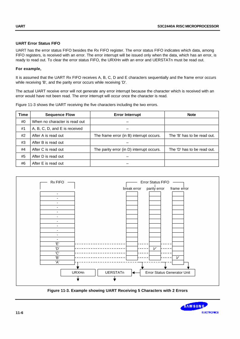
UART S3C2440A RISC MICROPROCESSOR
11-6
UART Error Status FIFO
UART has the error status FIFO besides the Rx FIFO register. The error status FIFO indicates which data, amongFIFO registers, is received with an error. The error interrupt will be issued only when the data, which has an error, isready to read out. To clear the error status FIFO, the URXHn with an error and UERSTATn must be read out.
For example,
It is assumed that the UART Rx FIFO receives A, B, C, D and E characters sequentially and the frame error occurswhile receiving 'B', and the parity error occurs while receiving 'D'.
The actual UART receive error will not generate any error interrupt because the character which is received with anerror would have not been read. The error interrupt will occur once the character is read.
Figure 11-3 shows the UART receiving the five characters including the two errors.
Time Sequence Flow Error Interrupt Note
#0 When no character is read out –
#1 A, B, C, D, and E is received –
#2 After A is read out The frame error (in B) interrupt occurs. The 'B' has to be read out.
#3 After B is read out –
#4 After C is read out The parity error (in D) interrupt occurs. The 'D' has to be read out.
#5 After D is read out –
#6 After E is read out –
-----------
'E''D''C''B''A'
Rx FIFO
URXHn UERSTATn
break error parity error frame error
Error Status Generator Unit
Error Status FIFO
Figure 11-3. Example showing UART Receiving 5 Characters with 2 Errors
S3C2440A RISC MICROPROCESSOR UART
11-7
Baud-rate Generation
Each UART's baud-rate generator provides the serial clock for the transmitter and the receiver. The source clock forthe baud-rate generator can be selected with the S3C2440A's internal system clock or UEXTCLK. In other words,dividend is selectable by setting Clock Selection of UCONn. The baud-rate clock is generated by dividing the sourceclock (PCLK, FCLK/n or UEXTCLK) by 16 and a 16-bit divisor specified in the UART baud-rate divisor register(UBRDIVn). The UBRDIVn can be determined by the following expression:
UBRDIVn = (int)( UART clock / ( buad rate x 16) ) –1
( UART clock: PCLK, FCLK/n or UEXTCLK )
Where, UBRDIVn should be from 1 to (216-1), but can be set 0 (bypass mode) only using the UEXTCLK whichshould be smaller than PCLK.
For example, if the baud-rate is 115200 bps and UART clock is 40 MHz, UBRDIVn is:
UBRDIVn = (int)(40000000 / (115200 x 16) ) -1= (int)(21.7) -1 [round to the nearest whole number]= 22 -1 = 21
Baud-Rate Error Tolerance
UART Frame error should be less than 1.87%(3/160).
tUPCLK = (UBRDIVn + 1) x 16 x 1Frame / PCLK tUPCLK: Real UART Clock
tUEXACT = 1Frame / baud-rate tUEXACT: Ideal UART Clock
UART error = (tUPCLK – tUEXACT) / tUEXACT x 100%
NOTES
1. 1Frame = start bit + data bit + parity bit + stop bit.2. In specific condition, we can support the UART baud rate up to 921.6K bps. For example, when PCLK is 60MHz, you can use 921.6K bps under UART error of 1.69%.
Loopback Mode
The S3C2440A UART provides a test mode referred to as the Loopback mode, to aid in isolating faults in thecommunication link. This mode structurally enables the connection of RXD and TXD in the UART. In this mode,therefore, transmitted data is received to the receiver, via RXD. This feature allows the processor to verify the internaltransmit and to receive the data path of each SIO channel. This mode can be selected by setting the loopback bit inthe UART control register (UCONn).

UART S3C2440A RISC MICROPROCESSOR
11-8
Infrared (IR) Mode
The S3C2440A UART block supports infrared (IR) transmission and reception, which can be selected by setting theInfrared-mode bit in the UART line control register (ULCONn). Figure 11-4 illustrates how to implement the IR mode.
In IR transmit mode, the transmit pulse comes out at a rate of 3/16, the normal serial transmit rate (when thetransmit data bit is zero); In IR receive mode, the receiver must detect the 3/16 pulsed period to recognize a zerovalue (see the frame timing diagrams shown in Figure 11-6 and 11-7).
IrDA TxEncoder
0
1
0
1
IrDA RxDecoder
TxD
RxD
TxD
IRS
RxD
RE
UARTBlock
Figure 11-4. IrDA Function Block Diagram
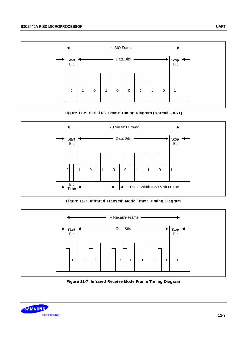
S3C2440A RISC MICROPROCESSOR UART
11-9
StartBit
StopBit
Data Bits
SIO Frame
0 1 0 1 0 0 1 1 0 1
Figure 11-5. Serial I/O Frame Timing Diagram (Normal UART)
0
StartBit
StopBit
Data Bits
IR Transmit Frame
BitTime Pulse Width = 3/16 Bit Frame
0 0 0 0 11111
Figure 11-6. Infrared Transmit Mode Frame Timing Diagram
0
StartBit
StopBit
Data Bits
IR Receive Frame
0 0 0 0 11111
Figure 11-7. Infrared Receive Mode Frame Timing Diagram

UART S3C2440A RISC MICROPROCESSOR
11-10
UART SPECIAL REGISTERS
UART LINE CONTROL REGISTER
There are three UART line control registers including ULCON0, ULCON1, and ULCON2 in the UART block.
Register Address R/W Description Reset Value
ULCON0 0x50000000 R/W UART channel 0 line control register 0x00
ULCON1 0x50004000 R/W UART channel 1 line control register 0x00
ULCON2 0x50008000 R/W UART channel 2 line control register 0x00
ULCONn Bit Description Initial State
Reserved [7] – 0
Infrared Mode [6] Determine whether or not to use the Infrared mode.
0 = Normal mode operation1 = Infrared Tx/Rx mode
0
Parity Mode [5:3] Specify the type of parity generation and checking during UARTtransmit and receive operation.
0xx = No parity100 = Odd parity101 = Even parity110 = Parity forced/checked as 1111 = Parity forced/checked as 0
000
Number of StopBit
[2] Specify how many stop bits are to be used for end-of-frame signal.
0 = One stop bit per frame1 = Two stop bit per frame
0
Word Length [1:0] Indicate the number of data bits to be transmitted or received perframe.
00 = 5-bits 01 = 6-bits10 = 7-bits 11 = 8-bits
00
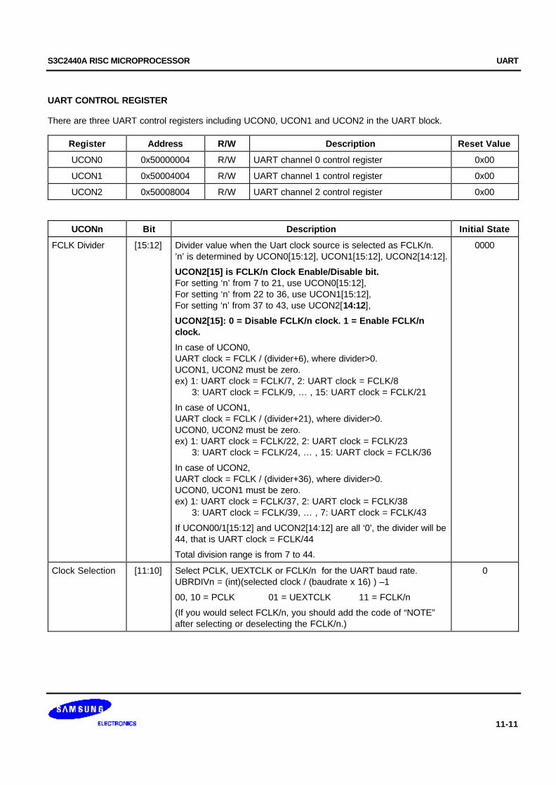
S3C2440A RISC MICROPROCESSOR UART
11-11
UART CONTROL REGISTER
There are three UART control registers including UCON0, UCON1 and UCON2 in the UART block.
Register Address R/W Description Reset Value
UCON0 0x50000004 R/W UART channel 0 control register 0x00
UCON1 0x50004004 R/W UART channel 1 control register 0x00
UCON2 0x50008004 R/W UART channel 2 control register 0x00
UCONn Bit Description Initial State
FCLK Divider [15:12] Divider value when the Uart clock source is selected as FCLK/n.’n’ is determined by UCON0[15:12], UCON1[15:12], UCON2[14:12].
UCON2[15] is FCLK/n Clock Enable/Disable bit.For setting ‘n’ from 7 to 21, use UCON0[15:12],For setting ‘n’ from 22 to 36, use UCON1[15:12],For setting ‘n’ from 37 to 43, use UCON2[14:12],
UCON2[15]: 0 = Disable FCLK/n clock. 1 = Enable FCLK/nclock.
In case of UCON0,UART clock = FCLK / (divider+6), where divider>0.UCON1, UCON2 must be zero.ex) 1: UART clock = FCLK/7, 2: UART clock = FCLK/8 3: UART clock = FCLK/9, … , 15: UART clock = FCLK/21
In case of UCON1,UART clock = FCLK / (divider+21), where divider>0.UCON0, UCON2 must be zero.ex) 1: UART clock = FCLK/22, 2: UART clock = FCLK/23 3: UART clock = FCLK/24, … , 15: UART clock = FCLK/36
In case of UCON2,UART clock = FCLK / (divider+36), where divider>0.UCON0, UCON1 must be zero.ex) 1: UART clock = FCLK/37, 2: UART clock = FCLK/38 3: UART clock = FCLK/39, … , 7: UART clock = FCLK/43
If UCON00/1[15:12] and UCON2[14:12] are all ‘0’, the divider will be44, that is UART clock = FCLK/44
Total division range is from 7 to 44.
0000
Clock Selection [11:10] Select PCLK, UEXTCLK or FCLK/n for the UART baud rate.UBRDIVn = (int)(selected clock / (baudrate x 16) ) –1
00, 10 = PCLK 01 = UEXTCLK 11 = FCLK/n
(If you would select FCLK/n, you should add the code of “NOTE”after selecting or deselecting the FCLK/n.)
0
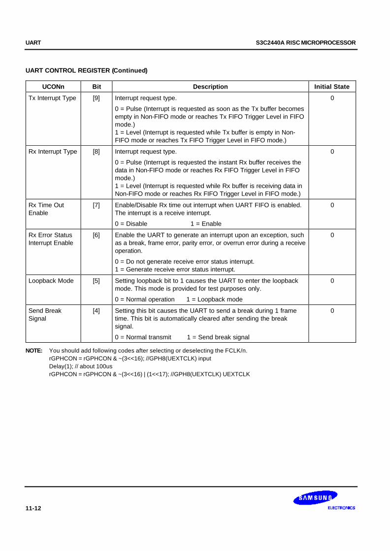
UART S3C2440A RISC MICROPROCESSOR
11-12
UART CONTROL REGISTER (Continued)
UCONn Bit Description Initial State
Tx Interrupt Type [9] Interrupt request type.
0 = Pulse (Interrupt is requested as soon as the Tx buffer becomesempty in Non-FIFO mode or reaches Tx FIFO Trigger Level in FIFOmode.)1 = Level (Interrupt is requested while Tx buffer is empty in Non-FIFO mode or reaches Tx FIFO Trigger Level in FIFO mode.)
0
Rx Interrupt Type [8] Interrupt request type.
0 = Pulse (Interrupt is requested the instant Rx buffer receives thedata in Non-FIFO mode or reaches Rx FIFO Trigger Level in FIFOmode.)1 = Level (Interrupt is requested while Rx buffer is receiving data inNon-FIFO mode or reaches Rx FIFO Trigger Level in FIFO mode.)
0
Rx Time OutEnable
[7] Enable/Disable Rx time out interrupt when UART FIFO is enabled.The interrupt is a receive interrupt.
0 = Disable 1 = Enable
0
Rx Error StatusInterrupt Enable
[6] Enable the UART to generate an interrupt upon an exception, suchas a break, frame error, parity error, or overrun error during a receiveoperation.
0 = Do not generate receive error status interrupt.1 = Generate receive error status interrupt.
0
Loopback Mode [5] Setting loopback bit to 1 causes the UART to enter the loopbackmode. This mode is provided for test purposes only.
0 = Normal operation 1 = Loopback mode
0
Send BreakSignal
[4] Setting this bit causes the UART to send a break during 1 frametime. This bit is automatically cleared after sending the breaksignal.
0 = Normal transmit 1 = Send break signal
0
NOTE: You should add following codes after selecting or deselecting the FCLK/n.rGPHCON = rGPHCON & ~(3<<16); //GPH8(UEXTCLK) inputDelay(1); // about 100usrGPHCON = rGPHCON & ~(3<<16) | (1<<17); //GPH8(UEXTCLK) UEXTCLK
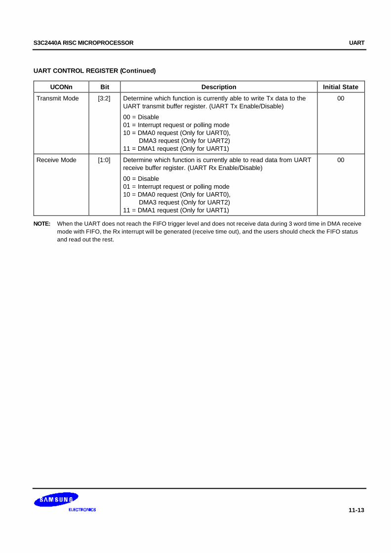
S3C2440A RISC MICROPROCESSOR UART
11-13
UART CONTROL REGISTER (Continued)
UCONn Bit Description Initial State
Transmit Mode [3:2] Determine which function is currently able to write Tx data to theUART transmit buffer register. (UART Tx Enable/Disable)
00 = Disable01 = Interrupt request or polling mode10 = DMA0 request (Only for UART0), DMA3 request (Only for UART2)11 = DMA1 request (Only for UART1)
00
Receive Mode [1:0] Determine which function is currently able to read data from UARTreceive buffer register. (UART Rx Enable/Disable)
00 = Disable01 = Interrupt request or polling mode10 = DMA0 request (Only for UART0), DMA3 request (Only for UART2)11 = DMA1 request (Only for UART1)
00
NOTE: When the UART does not reach the FIFO trigger level and does not receive data during 3 word time in DMA receivemode with FIFO, the Rx interrupt will be generated (receive time out), and the users should check the FIFO statusand read out the rest.
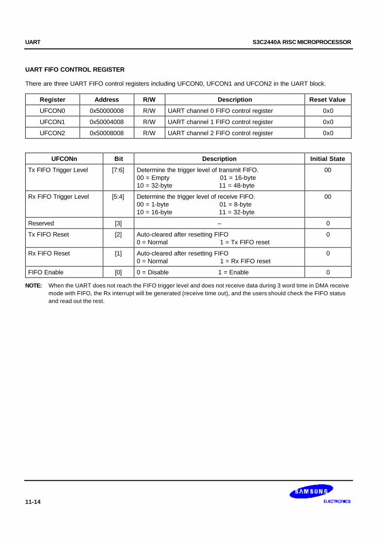
UART S3C2440A RISC MICROPROCESSOR
11-14
UART FIFO CONTROL REGISTER
There are three UART FIFO control registers including UFCON0, UFCON1 and UFCON2 in the UART block.
Register Address R/W Description Reset Value
UFCON0 0x50000008 R/W UART channel 0 FIFO control register 0x0
UFCON1 0x50004008 R/W UART channel 1 FIFO control register 0x0
UFCON2 0x50008008 R/W UART channel 2 FIFO control register 0x0
UFCONn Bit Description Initial State
Tx FIFO Trigger Level [7:6] Determine the trigger level of transmit FIFO.00 = Empty 01 = 16-byte10 = 32-byte 11 = 48-byte
00
Rx FIFO Trigger Level [5:4] Determine the trigger level of receive FIFO.00 = 1-byte 01 = 8-byte10 = 16-byte 11 = 32-byte
00
Reserved [3] – 0
Tx FIFO Reset [2] Auto-cleared after resetting FIFO0 = Normal 1 = Tx FIFO reset
0
Rx FIFO Reset [1] Auto-cleared after resetting FIFO0 = Normal 1 = Rx FIFO reset
0
FIFO Enable [0] 0 = Disable 1 = Enable 0
NOTE: When the UART does not reach the FIFO trigger level and does not receive data during 3 word time in DMA receive mode with FIFO, the Rx interrupt will be generated (receive time out), and the users should check the FIFO status and read out the rest.

S3C2440A RISC MICROPROCESSOR UART
11-15
UART MODEM CONTROL REGISTER
There are two UART MODEM control registers including UMCON0 and UMCON1 in the UART block.
Register Address R/W Description Reset Value
UMCON0 0x5000000C R/W UART channel 0 Modem control register 0x0
UMCON1 0x5000400C R/W UART channel 1 Modem control register 0x0
Reserved 0x5000800C – Reserved Undef
UMCONn Bit Description Initial State
Reserved [7:5] These bits must be 0's 00
Auto Flow Control(AFC)
[4] 0 = Disable 1 = Enable 0
Reserved [3:1] These bits must be 0's 00
Request to Send [0] If AFC bit is enabled, this value will be ignored. In this case theS3C2440A will control nRTS automatically.If AFC bit is disabled, nRTS must be controlled by software.
0 = 'H' level (Inactivate nRTS) 1 = 'L' level (Activate nRTS)
0
NOTE: UART 2 does not support AFC function, because the S3C2440A has no nRTS2 and nCTS2.
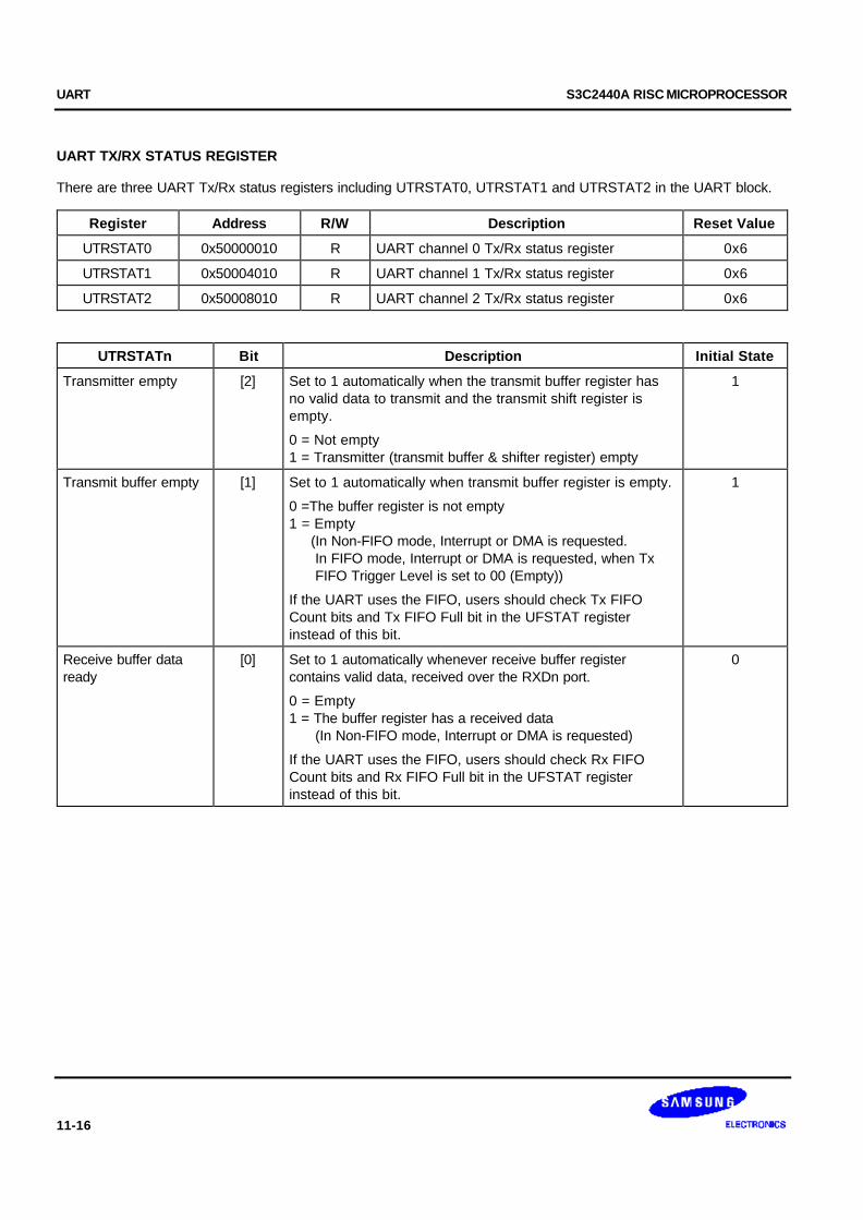
UART S3C2440A RISC MICROPROCESSOR
11-16
UART TX/RX STATUS REGISTER
There are three UART Tx/Rx status registers including UTRSTAT0, UTRSTAT1 and UTRSTAT2 in the UART block.
Register Address R/W Description Reset Value
UTRSTAT0 0x50000010 R UART channel 0 Tx/Rx status register 0x6
UTRSTAT1 0x50004010 R UART channel 1 Tx/Rx status register 0x6
UTRSTAT2 0x50008010 R UART channel 2 Tx/Rx status register 0x6
UTRSTATn Bit Description Initial State
Transmitter empty [2] Set to 1 automatically when the transmit buffer register hasno valid data to transmit and the transmit shift register isempty.
0 = Not empty1 = Transmitter (transmit buffer & shifter register) empty
1
Transmit buffer empty [1] Set to 1 automatically when transmit buffer register is empty.
0 =The buffer register is not empty1 = Empty (In Non-FIFO mode, Interrupt or DMA is requested. In FIFO mode, Interrupt or DMA is requested, when Tx FIFO Trigger Level is set to 00 (Empty))
If the UART uses the FIFO, users should check Tx FIFOCount bits and Tx FIFO Full bit in the UFSTAT registerinstead of this bit.
1
Receive buffer dataready
[0] Set to 1 automatically whenever receive buffer registercontains valid data, received over the RXDn port.
0 = Empty1 = The buffer register has a received data (In Non-FIFO mode, Interrupt or DMA is requested)
If the UART uses the FIFO, users should check Rx FIFOCount bits and Rx FIFO Full bit in the UFSTAT registerinstead of this bit.
0

S3C2440A RISC MICROPROCESSOR UART
11-17
UART ERROR STATUS REGISTER
There are three UART Rx error status registers including UERSTAT0, UERSTAT1 and UERSTAT2 in the UARTblock.
Register Address R/W Description Reset Value
UERSTAT0 0x50000014 R UART channel 0 Rx error status register 0x0
UERSTAT1 0x50004014 R UART channel 1 Rx error status register 0x0
UERSTAT2 0x50008014 R UART channel 2 Rx error status register 0x0
UERSTATn Bit Description Initial State
Break Detect [3] Set to 1 automatically to indicate that a break signal has beenreceived.
0 = No break receive1 = Break receive (Interrupt is requested.)
0
Frame Error [2] Set to 1 automatically whenever a frame error occurs duringreceive operation.
0 = No frame error during receive1 = Frame error (Interrupt is requested.)
0
Parity Error [1] Set to 1 automatically whenever a parity error occurs duringreceive operation.
0 = No parity error during receive1 = Parity error (Interrupt is requested.)
0
Overrun Error [0] Set to 1 automatically whenever an overrun error occurs duringreceive operation.
0 = No overrun error during receive1 = Overrun error (Interrupt is requested.)
0
NOTE: These bits (UERSATn[3:0]) are automatically cleared to 0 when the UART error status register is read.
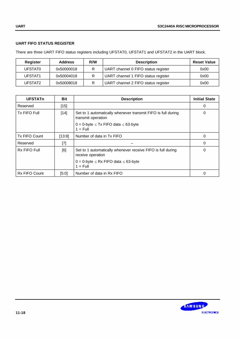
UART S3C2440A RISC MICROPROCESSOR
11-18
UART FIFO STATUS REGISTER
There are three UART FIFO status registers including UFSTAT0, UFSTAT1 and UFSTAT2 in the UART block.
Register Address R/W Description Reset Value
UFSTAT0 0x50000018 R UART channel 0 FIFO status register 0x00
UFSTAT1 0x50004018 R UART channel 1 FIFO status register 0x00
UFSTAT2 0x50008018 R UART channel 2 FIFO status register 0x00
UFSTATn Bit Description Initial State
Reserved [15] 0
Tx FIFO Full [14] Set to 1 automatically whenever transmit FIFO is full duringtransmit operation
0 = 0-byte ≤ Tx FIFO data ≤ 63-byte1 = Full
0
Tx FIFO Count [13:8] Number of data in Tx FIFO 0
Reserved [7] – 0
Rx FIFO Full [6] Set to 1 automatically whenever receive FIFO is full duringreceive operation
0 = 0-byte ≤ Rx FIFO data ≤ 63-byte1 = Full
0
Rx FIFO Count [5:0] Number of data in Rx FIFO 0
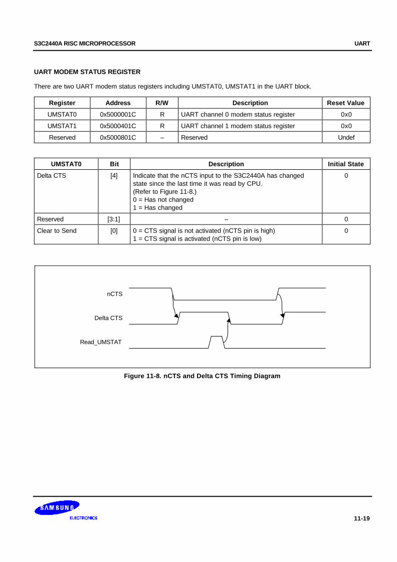
S3C2440A RISC MICROPROCESSOR UART
11-19
UART MODEM STATUS REGISTER
There are two UART modem status registers including UMSTAT0, UMSTAT1 in the UART block.
Register Address R/W Description Reset Value
UMSTAT0 0x5000001C R UART channel 0 modem status register 0x0
UMSTAT1 0x5000401C R UART channel 1 modem status register 0x0
Reserved 0x5000801C – Reserved Undef
UMSTAT0 Bit Description Initial State
Delta CTS [4] Indicate that the nCTS input to the S3C2440A has changedstate since the last time it was read by CPU.(Refer to Figure 11-8.)0 = Has not changed1 = Has changed
0
Reserved [3:1] – 0
Clear to Send [0] 0 = CTS signal is not activated (nCTS pin is high)1 = CTS signal is activated (nCTS pin is low)
0
nCTS
Delta CTS
Read_UMSTAT
Figure 11-8. nCTS and Delta CTS Timing Diagram

UART S3C2440A RISC MICROPROCESSOR
11-20
UART TRANSMIT BUFFER REGISTER (HOLDING REGISTER & FIFO REGISTER)
There are three UART transmit buffer registers including UTXH0, UTXH1 and UTXH2 in the UART block.UTXHn has an 8-bit data for transmission data.
Register Address R/W Description Reset Value
UTXH0 0x50000020(L)
0x50000023(B)
W(by byte)
UART channel 0 transmit buffer register –
UTXH1 0x50004020(L)
0x50004023(B)
W(by byte)
UART channel 1 transmit buffer register –
UTXH2 0x50008020(L)
0x50008023(B)
W(by byte)
UART channel 2 transmit buffer register –
UTXHn Bit Description Initial State
TXDATAn [7:0] Transmit data for UARTn –
NOTE: (L): The endian mode is Little endian.(B): The endian mode is Big endian.
UART RECEIVE BUFFER REGISTER (HOLDING REGISTER & FIFO REGISTER)
There are three UART receive buffer registers including URXH0, URXH1 and URXH2 in the UART block.URXHn has an 8-bit data for received data.
Register Address R/W Description Reset Value
URXH0 0x50000024(L)
0x50000027(B)
R(by byte)
UART channel 0 receive buffer register –
URXH1 0x50004024(L)0x50004027(B)
R(by byte)
UART channel 1 receive buffer register –
URXH2 0x50008024(L)0x50008027(B)
R(by byte)
UART channel 2 receive buffer register –
URXHn Bit Description Initial State
RXDATAn [7:0] Receive data for UARTn –
NOTE: When an overrun error occurs, the URXHn must be read. If not, the next received data will also make an overrun error, even though the overrun bit of UERSTATn had been cleared.
S3C2440A RISC MICROPROCESSOR UART
11-21
UART BAUD RATE DIVISOR REGISTER
There are three UART baud rate divisor registers including UBRDIV0, UBRDIV1 and UBRDIV2 in the UART block.The value stored in the baud rate divisor register (UBRDIVn), is used to determine the serial Tx/Rx clock rate (baudrate) as follows:
UBRDIVn = (int)( UART clock / ( buad rate x 16) ) –1
( UART clock: PCLK, FCLK/n or UEXTCLK )
Where, UBRDIVn should be from 1 to (216-1), but can be set zero only using the UEXTCLK which should be smallerthan PCLK.
For example, if the baud-rate is 115200 bps and UART clock is 40 MHz, UBRDIVn is:
UBRDIVn = (int)(40000000 / (115200 x 16) ) -1= (int)(21.7) -1 [round to the nearest whole number]= 22 -1 = 21
Register Address R/W Description Reset Value
UBRDIV0 0x50000028 R/W Baud rate divisior register 0 –
UBRDIV1 0x50004028 R/W Baud rate divisior register 1 –
UBRDIV2 0x50008028 R/W Baud rate divisior register 2 –
UBRDIVn Bit Description Initial State
UBRDIV [15:0] Baud rate division value UBRDIVn > 0Using the UEXTCLK as input clock, UBRDIVn can be set‘0’.
–

UART S3C2440A RISC MICROPROCESSOR
11-22
NOTES
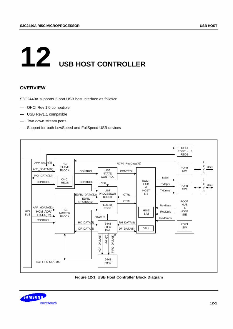
S3C2440A RISC MICROPROCESSOR USB HOST
12-1
12 USB HOST CONTROLLER
OVERVIEW
S3C2440A supports 2-port USB host interface as follows:
— OHCI Rev 1.0 compatible
— USB Rev1.1 compatible
— Two down stream ports
— Support for both LowSpeed and FullSpeed USB devices
HCISLAVEBLOCK
APP_SADR(8)
APP_SDATA(32)
HCI_DATA(32)
CONTROL
CONTROL
OHCIREGS
USBSTATE
CONTROL
LISTPROCESSOR
BLOCK
ED&TDREGS
Cntl
HCIMASTERBLOCK
CONTROL
ED/TD_DATA(32)ED/TD
STATUS(32)
64x8FIFOCntl
HC_DATA(8)
DF_DATA(8)
APP_MDATA(32)HCM_ADR/DATA(32)
CONTROLSTATUS
CONTROL
CTRL
CTRL
RH_DATA(8)
DF_DATA(8)
HC
F_D
AT
A(8
)
Add
r(6)
FIF
O_D
AT
A(8
)
64x8FIFO
ROOTHUB
&HOSTSIE
HSIES/M
DPLL
ROOTHUB
&HOSTSIE
OHCIROOT HUB
REGS
PORTS/M
PORTS/M
PORTS/M
XVR
USB
1
XVR
USB
2
HCIBUS
EXT.FIFO STATUS
RCF0_RegData(32)
TxEnl
TxDpls
TxDmns
RcvData
RcvDpls
RcvDmns
Figure 12-1. USB Host Controller Block Diagram
USB HOST S3C2440A RISC MICROPROCESSOR
12-2
USB HOST CONTROLLER SPECIAL REGISTERS
The S3C2440A USB host controller complies with OHCI Rev 1.0. Refer to Open Host Controller Interface Rev 1.0specification for detailed information.
OHCI REGISTERS FOR USB HOST CONTROLLER
Register Base Address R/W Description Reset Value
HcRevision 0x49000000 – Control and status group –
HcControl 0x49000004 – –
HcCommonStatus 0x49000008 – –
HcInterruptStatus 0x4900000C – –
HcInterruptEnable 0x49000010 – –
HcInterruptDisable 0x49000014 – –
HcHCCA 0x49000018 – Memory pointer group –
HcPeriodCuttentED 0x4900001C – –
HcControlHeadED 0x49000020 – –
HcControlCurrentED 0x49000024 – –
HcBulkHeadED 0x49000028 – –
HcBulkCurrentED 0x4900002C – –
HcDoneHead 0x49000030 – –
HcRmInterval 0x49000034 – Frame counter group –
HcFmRemaining 0x49000038 – –
HcFmNumber 0x4900003C – –
HcPeriodicStart 0x49000040 – –
HcLSThreshold 0x49000044 – –
HcRhDescriptorA 0x49000048 – Root hub group –
HcRhDescriptorB 0x4900004C – –
HcRhStatus 0x49000050 – –
HcRhPortStatus1 0x49000054 – –
HcRhPortStatus2 0x49000058 – –
S3C2440A RISC MICROPROCESSOR USB DEVICE
13-1
13 USB DEVICE CONTROLLER
OVERVIEW
Universal Serial Bus (USB) device controller is designed to provide a high performance full speed function controllersolution with DMA interface. USB device controller allows bulk transfer with DMA, interrupt transfer and controltransfer.
USB Device Controller Supports:
— Full speed USB device controller compatible with the USB specification version 1.1
— DMA interface for bulk transfer
— Five endpoints with FIFOEP0: 16byte (Register)EP1: 128byte IN/OUT FIFO (dual port asynchronous RAM): interrupt or DMAEP2: 128byte IN/OUT FIFO (dual port asynchronous RAM): interrupt or DMAEP3: 128byte IN/OUT FIFO (dual port asynchronous RAM): interrupt or DMAEP4: 128byte IN/OUT FIFO (dual port asynchronous RAM): interrupt or DMA
— Integrated USB Transceiver
FEATURE
— Fully compliant with USB Specification Version 1.1
— Full speed (12Mbps) device
— Integrated USB Transceiver
— Supports control, interrupt and bulk transfer
— Five endpoints with FIFO:One bi-directional control endpoint with 16-byte FIFO (EP0)Four bi-directional bulk endpoints with 128-byte FIFO (EP1, EP2, EP3, and EP4)
— Supports DMA interface for receive and transmit bulk endpoints. (EP1, EP2, EP3, and EP4)
— Independent 128-byte receive and transmit FIFO to maximize throughput
— Supports suspend and remote wakeup function
NOTE
PCLK should be more than 20MHz to use USB Controller in stable condition.
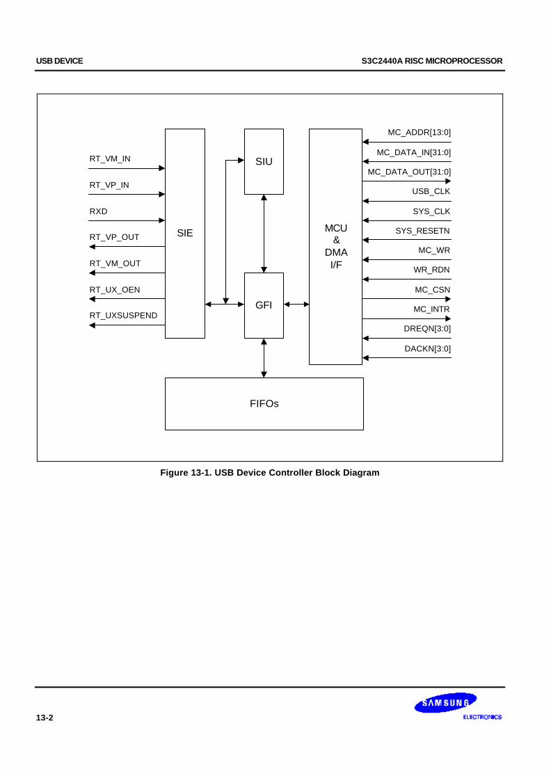
USB DEVICE S3C2440A RISC MICROPROCESSOR
13-2
SIERT_VP_OUT
RT_VM_IN
RT_VP_IN
RXD
RT_UXSUSPEND
RT_UX_OEN
RT_VM_OUT
MC_ADDR[13:0]
SIU
GFI
FIFOs
MCU&
DMAI/F
MC_DATA_IN[31:0]
MC_DATA_OUT[31:0]
USB_CLK
SYS_CLK
SYS_RESETN
MC_WR
WR_RDN
MC_CSN
MC_INTR
DREQN[3:0]
DACKN[3:0]
Figure 13-1. USB Device Controller Block Diagram
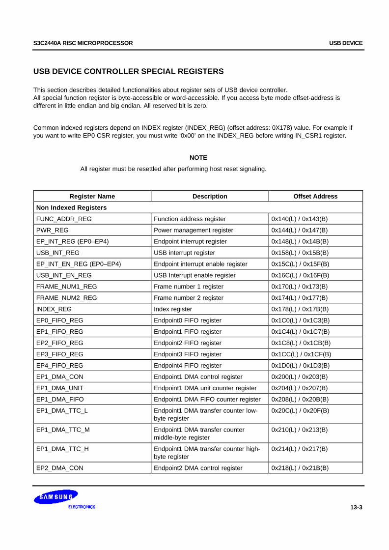
S3C2440A RISC MICROPROCESSOR USB DEVICE
13-3
USB DEVICE CONTROLLER SPECIAL REGISTERS
This section describes detailed functionalities about register sets of USB device controller.All special function register is byte-accessible or word-accessible. If you access byte mode offset-address isdifferent in little endian and big endian. All reserved bit is zero.
Common indexed registers depend on INDEX register (INDEX_REG) (offset address: 0X178) value. For example ifyou want to write EP0 CSR register, you must write ‘0x00’ on the INDEX_REG before writing IN_CSR1 register.
NOTE
All register must be resettled after performing host reset signaling.
Register Name Description Offset Address
Non Indexed Registers
FUNC_ADDR_REG Function address register 0x140(L) / 0x143(B)
PWR_REG Power management register 0x144(L) / 0x147(B)
EP_INT_REG (EP0–EP4) Endpoint interrupt register 0x148(L) / 0x14B(B)
USB_INT_REG USB interrupt register 0x158(L) / 0x15B(B)
EP_INT_EN_REG (EP0–EP4) Endpoint interrupt enable register 0x15C(L) / 0x15F(B)
USB_INT_EN_REG USB Interrupt enable register 0x16C(L) / 0x16F(B)
FRAME_NUM1_REG Frame number 1 register 0x170(L) / 0x173(B)
FRAME_NUM2_REG Frame number 2 register 0x174(L) / 0x177(B)
INDEX_REG Index register 0x178(L) / 0x17B(B)
EP0_FIFO_REG Endpoint0 FIFO register 0x1C0(L) / 0x1C3(B)
EP1_FIFO_REG Endpoint1 FIFO register 0x1C4(L) / 0x1C7(B)
EP2_FIFO_REG Endpoint2 FIFO register 0x1C8(L) / 0x1CB(B)
EP3_FIFO_REG Endpoint3 FIFO register 0x1CC(L) / 0x1CF(B)
EP4_FIFO_REG Endpoint4 FIFO register 0x1D0(L) / 0x1D3(B)
EP1_DMA_CON Endpoint1 DMA control register 0x200(L) / 0x203(B)
EP1_DMA_UNIT Endpoint1 DMA unit counter register 0x204(L) / 0x207(B)
EP1_DMA_FIFO Endpoint1 DMA FIFO counter register 0x208(L) / 0x20B(B)
EP1_DMA_TTC_L Endpoint1 DMA transfer counter low-byte register
0x20C(L) / 0x20F(B)
EP1_DMA_TTC_M Endpoint1 DMA transfer countermiddle-byte register
0x210(L) / 0x213(B)
EP1_DMA_TTC_H Endpoint1 DMA transfer counter high-byte register
0x214(L) / 0x217(B)
EP2_DMA_CON Endpoint2 DMA control register 0x218(L) / 0x21B(B)

USB DEVICE S3C2440A RISC MICROPROCESSOR
13-4
USB DEVICE CONTROLLER SPECIAL REGISTERS (Continued)
Register Name Description Offset Address
EP2_DMA_UNIT Endpoint2 DMA unit counter register 0x21C(L) / 0x21F(B)
EP2_DMA_FIFO Endpoint2 DMA FIFO counter register 0x220(L) / 0x223(B)
EP2_DMA_TTC_L Endpoint2 DMA transfer counter low-byte register
0x224(L) / 0x227(B)
EP2_DMA_TTC_M Endpoint2 DMA transfer countermiddle-byte register
0x228(L) / 0x22B(B)
EP2_DMA_TTC_H Endpoint2 DMA transfer counter high-byte register
0x22C(L) / 0x22F(B)
EP3_DMA_CON Endpoint3 DMA control register 0x240(L) / 0x243(B)
EP3_DMA_UNIT Endpoint3 DMA unit counter register 0x244(L) / 0x247(B)
EP3_DMA_FIFO Endpoint3 DMA FIFO counter register 0x248(L) / 0x24B(B)
EP3_DMA_TTC_L Endpoint3 DMA transfer counter low-byte register
0x24C(L) / 0x24F(B)
EP3_DMA_TTC_M Endpoint3 DMA transfer countermiddle-byte register
0x250(L) / 0x253(B)
EP3_DMA_TTC_H Endpoint3 DMA transfer counter high-byte register
0x254(L) / 0x247(B)
EP4_DMA_CON Endpoint4 DMA control register 0x258(L) / 0x25B(B)
EP4_DMA_UNIT Endpoint4 DMA unit counter register 0x25C(L) / 0x25F(B)
EP4_DMA_FIFO Endpoint4 DMA FIFO counter register 0x260(L) / 0x263(B)
EP4_DMA_TTC_L Endpoint4 DMA transfer counter low-byte register
0x264(L) / 0x267(B)
EP4_DMA_TTC_M Endpoint4 DMA transfer countermiddle-byte register
0x268(L) / 0x26B(B)
EP4_DMA_TTC_H Endpoint4 DMA transfer counter high-byte register
0x26C(L) / 0x26F(B)
Common Indexed Registers
MAXP_REG Endpoint MAX packet register 0x180(L) / 0x183(B)
In Indexed Registers
IN_CSR1_REG/EP0_CSR EP In control status register 1/EP0control status register
0x184(L) / 0x187(B)
IN_CSR2_REG EP In control status register 2 0x188(L) / 0x18B(B)
Out Indexed Registers
OUT_CSR1_REG EP out control status register 1 0x190(L) / 0x193(B)
OUT_CSR2_REG EP out control status register 2 0x194(L) / 0x197(B)
OUT_FIFO_CNT1_REG EP out write count register 1 0x198(L) / 0x19B(B)
OUT_FIFO_CNT2_REG EP out write count register 2 0x19C(L) / 0x19F(B)

S3C2440A RISC MICROPROCESSOR USB DEVICE
13-5
FUNCTION ADDRESS REGISTER (FUNC_ADDR_REG)
This register maintains the USB device controller address assigned by the host. The Micro Controller Unit (MCU)writes the value received through a SET_ADDRESS descriptor to this register. This address is used for the nexttoken.
Register Address R/W Description Reset Value
FUNC_ADDR_REG 0x52000140(L)0x52000143(B)
R/W(byte)
Function address register 0x00
FUNC_ADDR_REG Bit MCU USB Description Initial State
ADDR_UPDATE [7] R/SET
R/CLEAR
Set by the MCU whenever it updates theFUNCTION_ADDR field in this register.
This bit will be cleared by USB whenDATA_END bit in EP0_CSR register.
0
FUNCTION_ADDR [6:0] R/W R The MCU write the unique address,assigned by host, to this field.
00
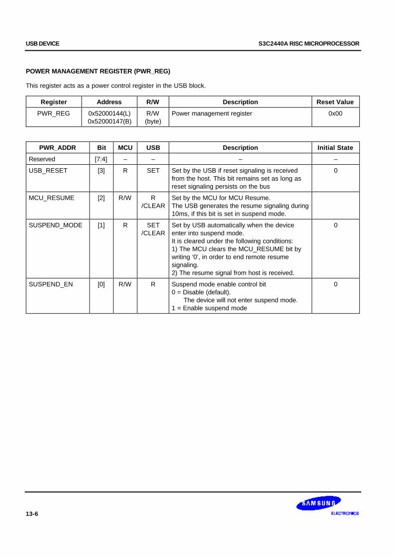
USB DEVICE S3C2440A RISC MICROPROCESSOR
13-6
POWER MANAGEMENT REGISTER (PWR_REG)
This register acts as a power control register in the USB block.
Register Address R/W Description Reset Value
PWR_REG 0x52000144(L)0x52000147(B)
R/W(byte)
Power management register 0x00
PWR_ADDR Bit MCU USB Description Initial State
Reserved [7:4] – – – –
USB_RESET [3] R SET Set by the USB if reset signaling is receivedfrom the host. This bit remains set as long asreset signaling persists on the bus
0
MCU_RESUME [2] R/W R/CLEAR
Set by the MCU for MCU Resume.The USB generates the resume signaling during10ms, if this bit is set in suspend mode.
SUSPEND_MODE [1] R SET/CLEAR
Set by USB automatically when the deviceenter into suspend mode.It is cleared under the following conditions:1) The MCU clears the MCU_RESUME bit bywriting ‘0’, in order to end remote resumesignaling.2) The resume signal from host is received.
0
SUSPEND_EN [0] R/W R Suspend mode enable control bit0 = Disable (default). The device will not enter suspend mode.1 = Enable suspend mode
0
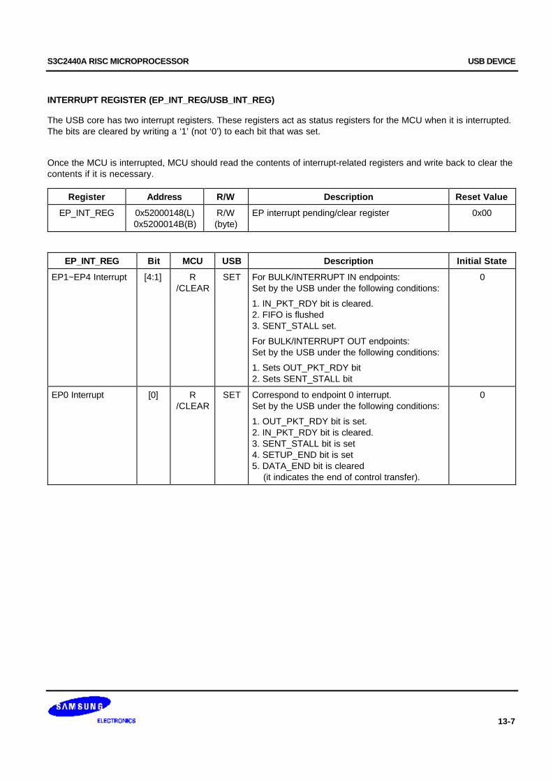
S3C2440A RISC MICROPROCESSOR USB DEVICE
13-7
INTERRUPT REGISTER (EP_INT_REG/USB_INT_REG)
The USB core has two interrupt registers. These registers act as status registers for the MCU when it is interrupted.The bits are cleared by writing a ‘1’ (not ‘0’) to each bit that was set.
Once the MCU is interrupted, MCU should read the contents of interrupt-related registers and write back to clear thecontents if it is necessary.
Register Address R/W Description Reset Value
EP_INT_REG 0x52000148(L)0x5200014B(B)
R/W(byte)
EP interrupt pending/clear register 0x00
EP_INT_REG Bit MCU USB Description Initial State
EP1~EP4 Interrupt [4:1] R/CLEAR
SET For BULK/INTERRUPT IN endpoints:Set by the USB under the following conditions:
1. IN_PKT_RDY bit is cleared.2. FIFO is flushed3. SENT_STALL set.
For BULK/INTERRUPT OUT endpoints:Set by the USB under the following conditions:
1. Sets OUT_PKT_RDY bit2. Sets SENT_STALL bit
0
EP0 Interrupt [0] R/CLEAR
SET Correspond to endpoint 0 interrupt.Set by the USB under the following conditions:
1. OUT_PKT_RDY bit is set.2. IN_PKT_RDY bit is cleared.3. SENT_STALL bit is set4. SETUP_END bit is set5. DATA_END bit is cleared (it indicates the end of control transfer).
0
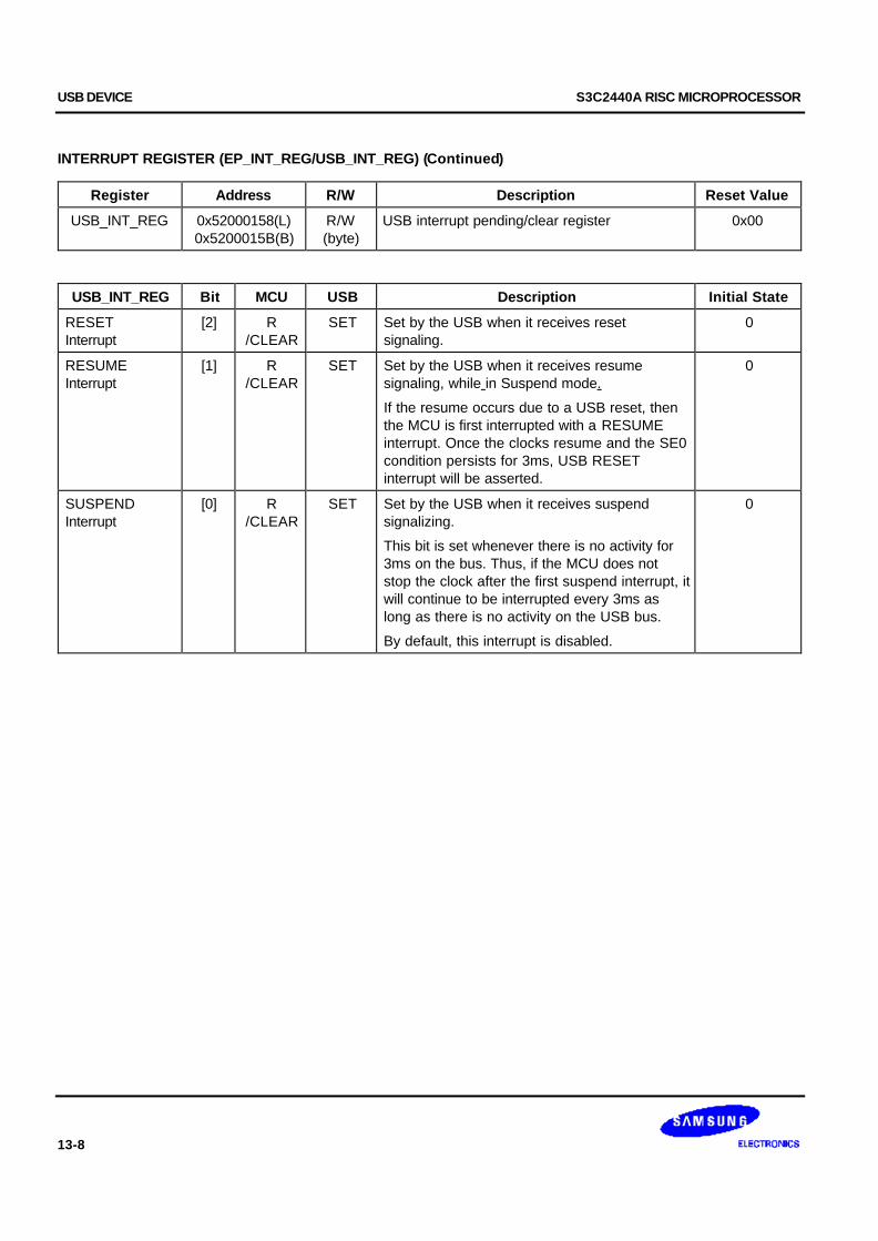
USB DEVICE S3C2440A RISC MICROPROCESSOR
13-8
INTERRUPT REGISTER (EP_INT_REG/USB_INT_REG) (Continued)
Register Address R/W Description Reset Value
USB_INT_REG 0x52000158(L)0x5200015B(B)
R/W(byte)
USB interrupt pending/clear register 0x00
USB_INT_REG Bit MCU USB Description Initial State
RESETInterrupt
[2] R/CLEAR
SET Set by the USB when it receives resetsignaling.
0
RESUMEInterrupt
[1] R/CLEAR
SET Set by the USB when it receives resumesignaling, while in Suspend mode.
If the resume occurs due to a USB reset, thenthe MCU is first interrupted with a RESUMEinterrupt. Once the clocks resume and the SE0condition persists for 3ms, USB RESETinterrupt will be asserted.
0
SUSPENDInterrupt
[0] R/CLEAR
SET Set by the USB when it receives suspendsignalizing.
This bit is set whenever there is no activity for3ms on the bus. Thus, if the MCU does notstop the clock after the first suspend interrupt, itwill continue to be interrupted every 3ms aslong as there is no activity on the USB bus.
By default, this interrupt is disabled.
0
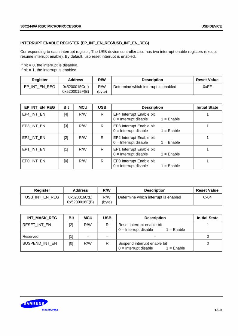
S3C2440A RISC MICROPROCESSOR USB DEVICE
13-9
INTERRUPT ENABLE REGISTER (EP_INT_EN_REG/USB_INT_EN_REG)
Corresponding to each interrupt register, The USB device controller also has two interrupt enable registers (exceptresume interrupt enable). By default, usb reset interrupt is enabled.
If bit = 0, the interrupt is disabled.If bit = 1, the interrupt is enabled.
Register Address R/W Description Reset Value
EP_INT_EN_REG 0x5200015C(L)0x5200015F(B)
R/W(byte)
Determine which interrupt is enabled 0xFF
EP_INT_EN_REG Bit MCU USB Description Initial State
EP4_INT_EN [4] R/W R EP4 Interrupt Enable bit0 = Interrupt disable 1 = Enable
1
EP3_INT_EN [3] R/W R EP3 Interrupt Enable bit0 = Interrupt disable 1 = Enable
1
EP2_INT_EN [2] R/W R EP2 Interrupt Enable bit0 = Interrupt disable 1 = Enable
1
EP1_INT_EN [1] R/W R EP1 Interrupt Enable bit0 = Interrupt disable 1 = Enable
1
EP0_INT_EN [0] R/W R EP0 Interrupt Enable bit0 = Interrupt disable 1 = Enable
1
Register Address R/W Description Reset Value
USB_INT_EN_REG 0x520016C(L)0x5200016F(B)
R/W(byte)
Determine which interrupt is enabled 0x04
INT_MASK_REG Bit MCU USB Description Initial State
RESET_INT_EN [2] R/W R Reset interrupt enable bit0 = Interrupt disable 1 = Enable
1
Reserved [1] – – – 0
SUSPEND_INT_EN [0] R/W R Suspend interrupt enable bit0 = Interrupt disable 1 = Enable
0
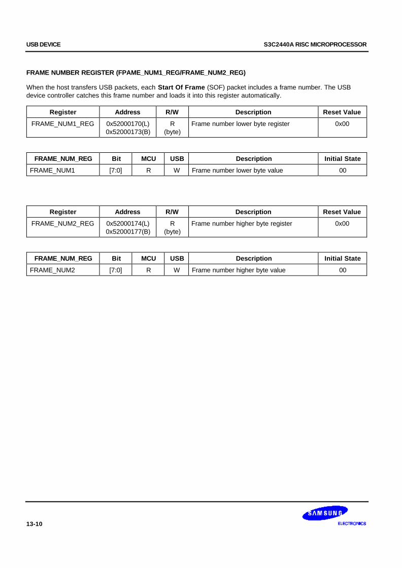
USB DEVICE S3C2440A RISC MICROPROCESSOR
13-10
FRAME NUMBER REGISTER (FPAME_NUM1_REG/FRAME_NUM2_REG)
When the host transfers USB packets, each Start Of Frame (SOF) packet includes a frame number. The USBdevice controller catches this frame number and loads it into this register automatically.
Register Address R/W Description Reset Value
FRAME_NUM1_REG 0x52000170(L)0x52000173(B)
R(byte)
Frame number lower byte register 0x00
FRAME_NUM_REG Bit MCU USB Description Initial State
FRAME_NUM1 [7:0] R W Frame number lower byte value 00
Register Address R/W Description Reset Value
FRAME_NUM2_REG 0x52000174(L)0x52000177(B)
R(byte)
Frame number higher byte register 0x00
FRAME_NUM_REG Bit MCU USB Description Initial State
FRAME_NUM2 [7:0] R W Frame number higher byte value 00
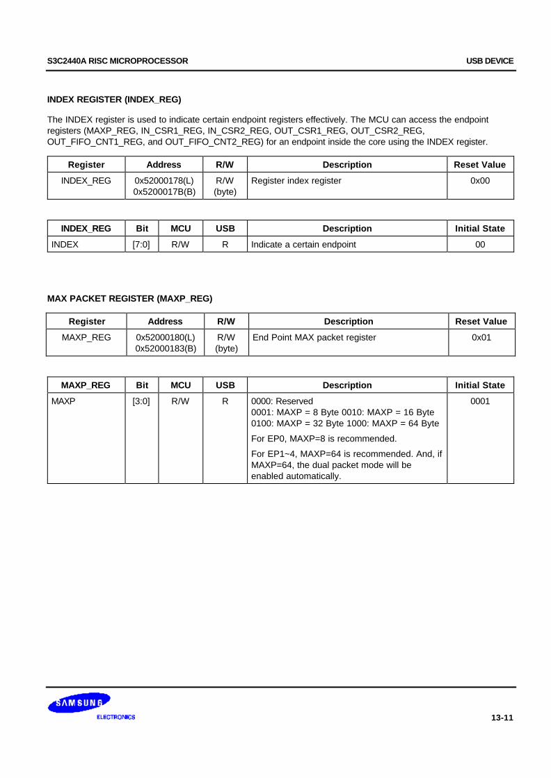
S3C2440A RISC MICROPROCESSOR USB DEVICE
13-11
INDEX REGISTER (INDEX_REG)
The INDEX register is used to indicate certain endpoint registers effectively. The MCU can access the endpointregisters (MAXP_REG, IN_CSR1_REG, IN_CSR2_REG, OUT_CSR1_REG, OUT_CSR2_REG,OUT_FIFO_CNT1_REG, and OUT_FIFO_CNT2_REG) for an endpoint inside the core using the INDEX register.
Register Address R/W Description Reset Value
INDEX_REG 0x52000178(L)0x5200017B(B)
R/W(byte)
Register index register 0x00
INDEX_REG Bit MCU USB Description Initial State
INDEX [7:0] R/W R Indicate a certain endpoint 00
MAX PACKET REGISTER (MAXP_REG)
Register Address R/W Description Reset Value
MAXP_REG 0x52000180(L)0x52000183(B)
R/W(byte)
End Point MAX packet register 0x01
MAXP_REG Bit MCU USB Description Initial State
MAXP [3:0] R/W R 0000: Reserved0001: MAXP = 8 Byte 0010: MAXP = 16 Byte0100: MAXP = 32 Byte 1000: MAXP = 64 Byte
For EP0, MAXP=8 is recommended.
For EP1~4, MAXP=64 is recommended. And, ifMAXP=64, the dual packet mode will beenabled automatically.
0001
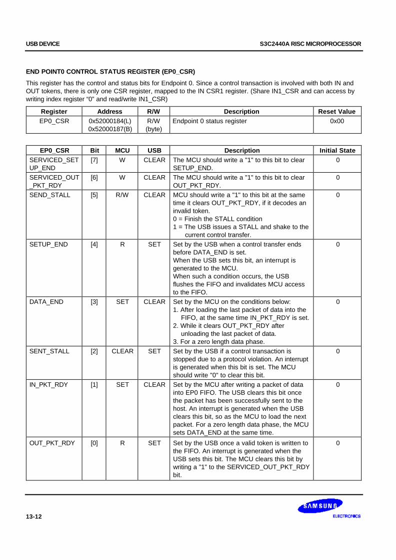
USB DEVICE S3C2440A RISC MICROPROCESSOR
13-12
END POINT0 CONTROL STATUS REGISTER (EP0_CSR)
This register has the control and status bits for Endpoint 0. Since a control transaction is involved with both IN andOUT tokens, there is only one CSR register, mapped to the IN CSR1 register. (Share IN1_CSR and can access bywriting index register “0” and read/write IN1_CSR)
Register Address R/W Description Reset ValueEP0_CSR 0x52000184(L)
0x52000187(B)R/W(byte)
Endpoint 0 status register 0x00
EP0_CSR Bit MCU USB Description Initial StateSERVICED_SETUP_END
[7] W CLEAR The MCU should write a "1" to this bit to clearSETUP_END.
0
SERVICED_OUT_PKT_RDY
[6] W CLEAR The MCU should write a "1" to this bit to clearOUT_PKT_RDY.
0
SEND_STALL [5] R/W CLEAR MCU should write a "1" to this bit at the sametime it clears OUT_PKT_RDY, if it decodes aninvalid token.0 = Finish the STALL condition1 = The USB issues a STALL and shake to the current control transfer.
0
SETUP_END [4] R SET Set by the USB when a control transfer endsbefore DATA_END is set.When the USB sets this bit, an interrupt isgenerated to the MCU.When such a condition occurs, the USBflushes the FIFO and invalidates MCU accessto the FIFO.
0
DATA_END [3] SET CLEAR Set by the MCU on the conditions below:1. After loading the last packet of data into the FIFO, at the same time IN_PKT_RDY is set.2. While it clears OUT_PKT_RDY after unloading the last packet of data.3. For a zero length data phase.
0
SENT_STALL [2] CLEAR SET Set by the USB if a control transaction isstopped due to a protocol violation. An interruptis generated when this bit is set. The MCUshould write "0" to clear this bit.
0
IN_PKT_RDY [1] SET CLEAR Set by the MCU after writing a packet of datainto EP0 FIFO. The USB clears this bit oncethe packet has been successfully sent to thehost. An interrupt is generated when the USBclears this bit, so as the MCU to load the nextpacket. For a zero length data phase, the MCUsets DATA_END at the same time.
0
OUT_PKT_RDY [0] R SET Set by the USB once a valid token is written tothe FIFO. An interrupt is generated when theUSB sets this bit. The MCU clears this bit bywriting a "1" to the SERVICED_OUT_PKT_RDYbit.
0
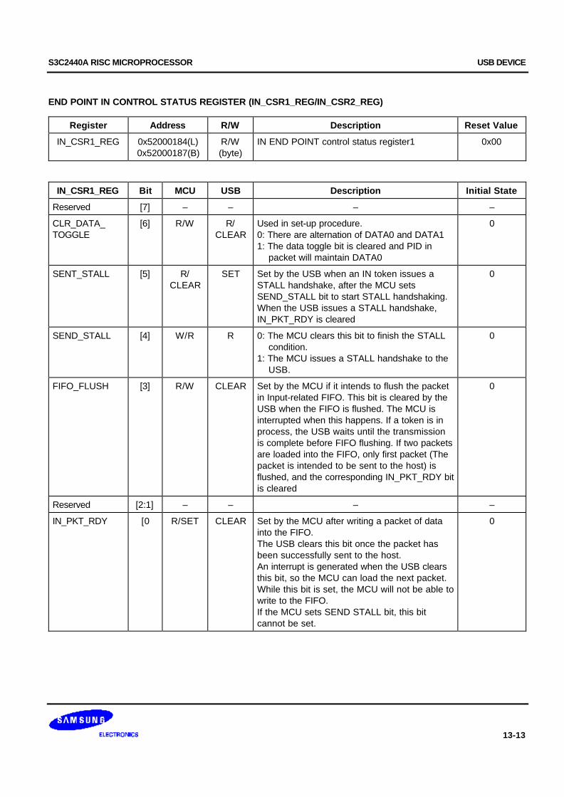
S3C2440A RISC MICROPROCESSOR USB DEVICE
13-13
END POINT IN CONTROL STATUS REGISTER (IN_CSR1_REG/IN_CSR2_REG)
Register Address R/W Description Reset Value
IN_CSR1_REG 0x52000184(L)0x52000187(B)
R/W(byte)
IN END POINT control status register1 0x00
IN_CSR1_REG Bit MCU USB Description Initial State
Reserved [7] – – – –
CLR_DATA_TOGGLE
[6] R/W R/CLEAR
Used in set-up procedure.0: There are alternation of DATA0 and DATA11: The data toggle bit is cleared and PID in packet will maintain DATA0
0
SENT_STALL [5] R/CLEAR
SET Set by the USB when an IN token issues aSTALL handshake, after the MCU setsSEND_STALL bit to start STALL handshaking.When the USB issues a STALL handshake,IN_PKT_RDY is cleared
0
SEND_STALL [4] W/R R 0: The MCU clears this bit to finish the STALL condition.1: The MCU issues a STALL handshake to the USB.
0
FIFO_FLUSH [3] R/W CLEAR Set by the MCU if it intends to flush the packetin Input-related FIFO. This bit is cleared by theUSB when the FIFO is flushed. The MCU isinterrupted when this happens. If a token is inprocess, the USB waits until the transmissionis complete before FIFO flushing. If two packetsare loaded into the FIFO, only first packet (Thepacket is intended to be sent to the host) isflushed, and the corresponding IN_PKT_RDY bitis cleared
0
Reserved [2:1] – – – –
IN_PKT_RDY [0 R/SET CLEAR Set by the MCU after writing a packet of datainto the FIFO.The USB clears this bit once the packet hasbeen successfully sent to the host.An interrupt is generated when the USB clearsthis bit, so the MCU can load the next packet.While this bit is set, the MCU will not be able towrite to the FIFO.If the MCU sets SEND STALL bit, this bitcannot be set.
0
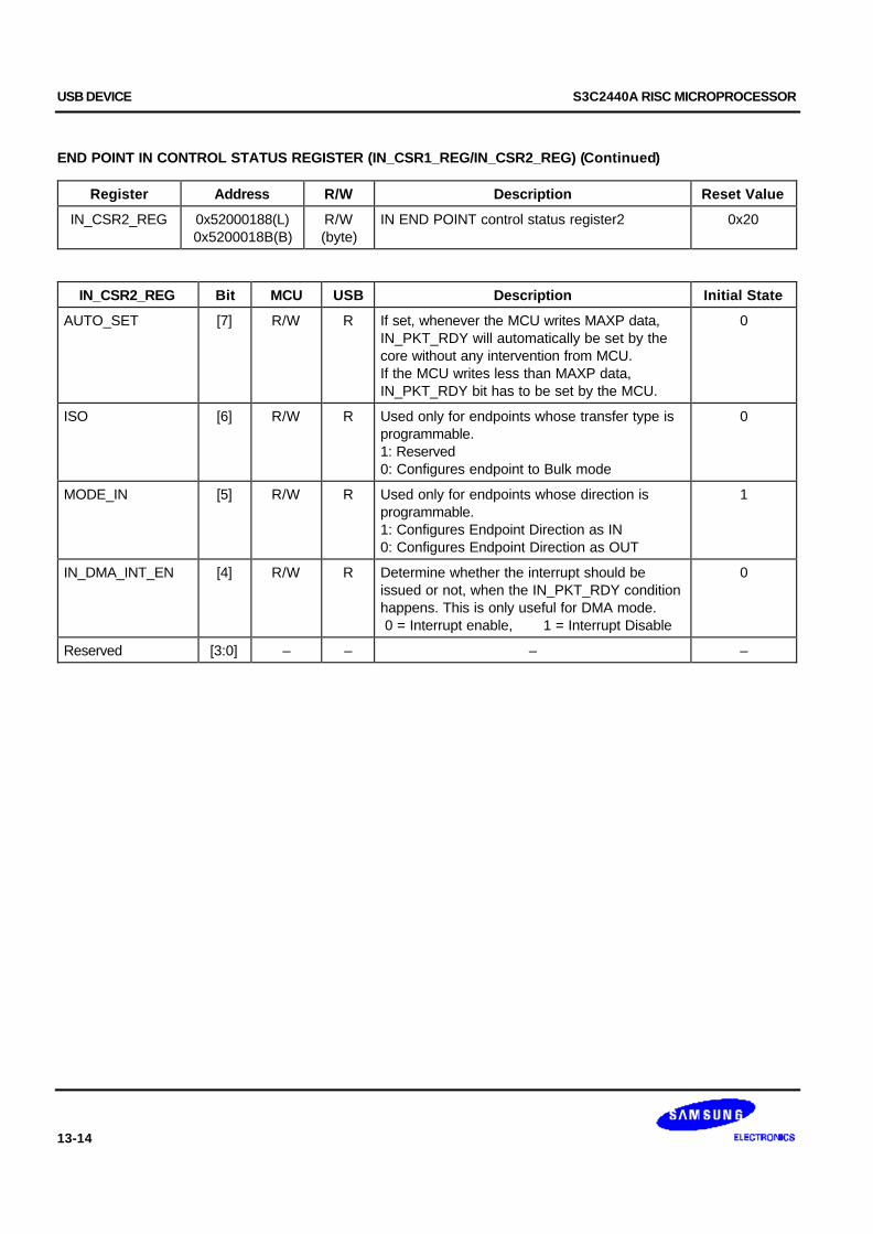
USB DEVICE S3C2440A RISC MICROPROCESSOR
13-14
END POINT IN CONTROL STATUS REGISTER (IN_CSR1_REG/IN_CSR2_REG) (Continued)
Register Address R/W Description Reset Value
IN_CSR2_REG 0x52000188(L)0x5200018B(B)
R/W(byte)
IN END POINT control status register2 0x20
IN_CSR2_REG Bit MCU USB Description Initial State
AUTO_SET [7] R/W R If set, whenever the MCU writes MAXP data,IN_PKT_RDY will automatically be set by thecore without any intervention from MCU.If the MCU writes less than MAXP data,IN_PKT_RDY bit has to be set by the MCU.
0
ISO [6] R/W R Used only for endpoints whose transfer type isprogrammable.1: Reserved0: Configures endpoint to Bulk mode
0
MODE_IN [5] R/W R Used only for endpoints whose direction isprogrammable.1: Configures Endpoint Direction as IN0: Configures Endpoint Direction as OUT
1
IN_DMA_INT_EN [4] R/W R Determine whether the interrupt should beissued or not, when the IN_PKT_RDY conditionhappens. This is only useful for DMA mode. 0 = Interrupt enable, 1 = Interrupt Disable
0
Reserved [3:0] – – – –
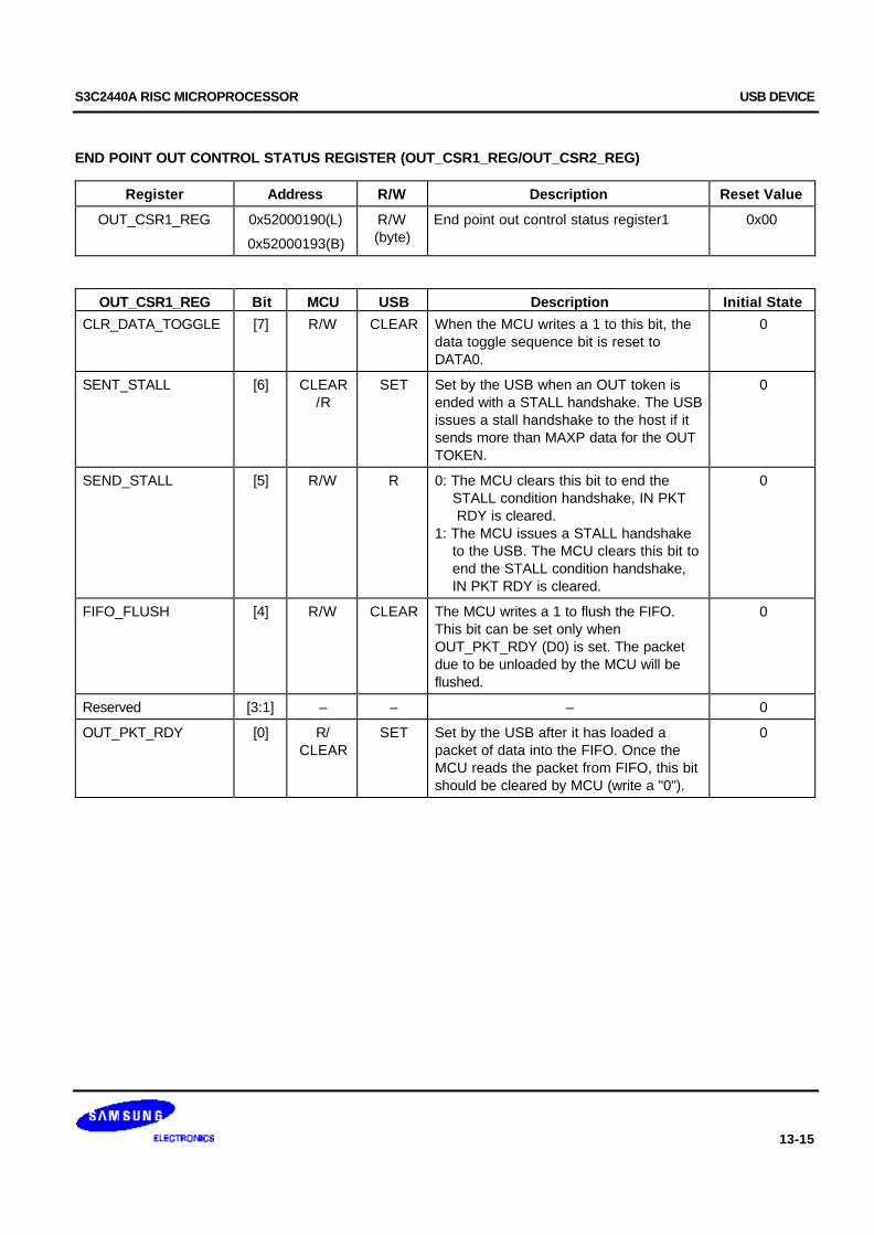
S3C2440A RISC MICROPROCESSOR USB DEVICE
13-15
END POINT OUT CONTROL STATUS REGISTER (OUT_CSR1_REG/OUT_CSR2_REG)
Register Address R/W Description Reset Value
OUT_CSR1_REG 0x52000190(L)
0x52000193(B)
R/W(byte)
End point out control status register1 0x00
OUT_CSR1_REG Bit MCU USB Description Initial State
CLR_DATA_TOGGLE [7] R/W CLEAR When the MCU writes a 1 to this bit, thedata toggle sequence bit is reset toDATA0.
0
SENT_STALL [6] CLEAR/R
SET Set by the USB when an OUT token isended with a STALL handshake. The USBissues a stall handshake to the host if itsends more than MAXP data for the OUTTOKEN.
0
SEND_STALL [5] R/W R 0: The MCU clears this bit to end the STALL condition handshake, IN PKT RDY is cleared.1: The MCU issues a STALL handshake to the USB. The MCU clears this bit to end the STALL condition handshake, IN PKT RDY is cleared.
0
FIFO_FLUSH [4] R/W CLEAR The MCU writes a 1 to flush the FIFO.This bit can be set only whenOUT_PKT_RDY (D0) is set. The packetdue to be unloaded by the MCU will beflushed.
0
Reserved [3:1] – – – 0
OUT_PKT_RDY [0] R/CLEAR
SET Set by the USB after it has loaded apacket of data into the FIFO. Once theMCU reads the packet from FIFO, this bitshould be cleared by MCU (write a "0").
0
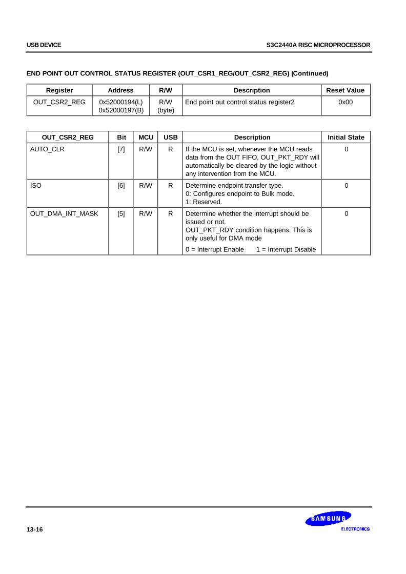
USB DEVICE S3C2440A RISC MICROPROCESSOR
13-16
END POINT OUT CONTROL STATUS REGISTER (OUT_CSR1_REG/OUT_CSR2_REG) (Continued)
Register Address R/W Description Reset Value
OUT_CSR2_REG 0x52000194(L)0x52000197(B)
R/W(byte)
End point out control status register2 0x00
OUT_CSR2_REG Bit MCU USB Description Initial State
AUTO_CLR [7] R/W R If the MCU is set, whenever the MCU readsdata from the OUT FIFO, OUT_PKT_RDY willautomatically be cleared by the logic withoutany intervention from the MCU.
0
ISO [6] R/W R Determine endpoint transfer type.0: Configures endpoint to Bulk mode.1: Reserved.
0
OUT_DMA_INT_MASK [5] R/W R Determine whether the interrupt should beissued or not.OUT_PKT_RDY condition happens. This isonly useful for DMA mode
0 = Interrupt Enable 1 = Interrupt Disable
0
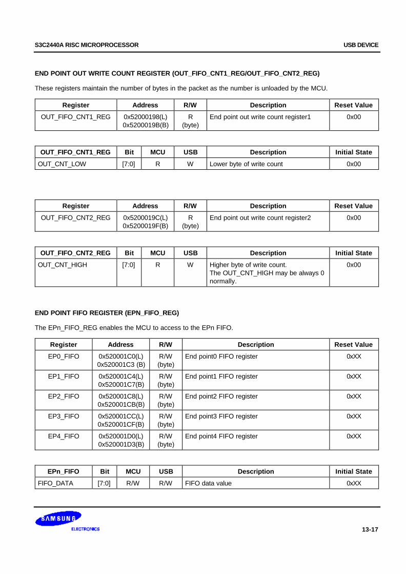
S3C2440A RISC MICROPROCESSOR USB DEVICE
13-17
END POINT OUT WRITE COUNT REGISTER (OUT_FIFO_CNT1_REG/OUT_FIFO_CNT2_REG)
These registers maintain the number of bytes in the packet as the number is unloaded by the MCU.
Register Address R/W Description Reset Value
OUT_FIFO_CNT1_REG 0x52000198(L)0x5200019B(B)
R(byte)
End point out write count register1 0x00
OUT_FIFO_CNT1_REG Bit MCU USB Description Initial State
OUT_CNT_LOW [7:0] R W Lower byte of write count 0x00
Register Address R/W Description Reset Value
OUT_FIFO_CNT2_REG 0x5200019C(L)0x5200019F(B)
R(byte)
End point out write count register2 0x00
OUT_FIFO_CNT2_REG Bit MCU USB Description Initial State
OUT_CNT_HIGH [7:0] R W Higher byte of write count.The OUT_CNT_HIGH may be always 0normally.
0x00
END POINT FIFO REGISTER (EPN_FIFO_REG)
The EPn_FIFO_REG enables the MCU to access to the EPn FIFO.
Register Address R/W Description Reset Value
EP0_FIFO 0x520001C0(L)0x520001C3 (B)
R/W(byte)
End point0 FIFO register 0xXX
EP1_FIFO 0x520001C4(L)0x520001C7(B)
R/W(byte)
End point1 FIFO register 0xXX
EP2_FIFO 0x520001C8(L)0x520001CB(B)
R/W(byte)
End point2 FIFO register 0xXX
EP3_FIFO 0x520001CC(L)0x520001CF(B)
R/W(byte)
End point3 FIFO register 0xXX
EP4_FIFO 0x520001D0(L)0x520001D3(B)
R/W(byte)
End point4 FIFO register 0xXX
EPn_FIFO Bit MCU USB Description Initial State
FIFO_DATA [7:0] R/W R/W FIFO data value 0xXX
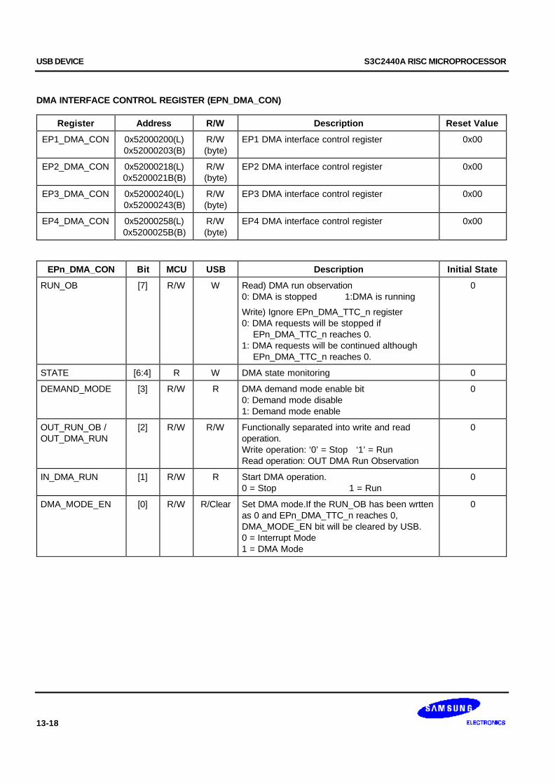
USB DEVICE S3C2440A RISC MICROPROCESSOR
13-18
DMA INTERFACE CONTROL REGISTER (EPN_DMA_CON)
Register Address R/W Description Reset Value
EP1_DMA_CON 0x52000200(L)0x52000203(B)
R/W(byte)
EP1 DMA interface control register 0x00
EP2_DMA_CON 0x52000218(L)0x5200021B(B)
R/W(byte)
EP2 DMA interface control register 0x00
EP3_DMA_CON 0x52000240(L)0x52000243(B)
R/W(byte)
EP3 DMA interface control register 0x00
EP4_DMA_CON 0x52000258(L)0x5200025B(B)
R/W(byte)
EP4 DMA interface control register 0x00
EPn_DMA_CON Bit MCU USB Description Initial State
RUN_OB [7] R/W W Read) DMA run observation0: DMA is stopped 1:DMA is running
Write) Ignore EPn_DMA_TTC_n register0: DMA requests will be stopped if EPn_DMA_TTC_n reaches 0.1: DMA requests will be continued although EPn_DMA_TTC_n reaches 0.
0
STATE [6:4] R W DMA state monitoring 0
DEMAND_MODE [3] R/W R DMA demand mode enable bit0: Demand mode disable1: Demand mode enable
0
OUT_RUN_OB /OUT_DMA_RUN
[2] R/W R/W Functionally separated into write and readoperation.Write operation: ‘0’ = Stop ‘1’ = RunRead operation: OUT DMA Run Observation
0
IN_DMA_RUN [1] R/W R Start DMA operation.0 = Stop 1 = Run
0
DMA_MODE_EN [0] R/W R/Clear Set DMA mode.If the RUN_OB has been wrttenas 0 and EPn_DMA_TTC_n reaches 0,DMA_MODE_EN bit will be cleared by USB.0 = Interrupt Mode1 = DMA Mode
0
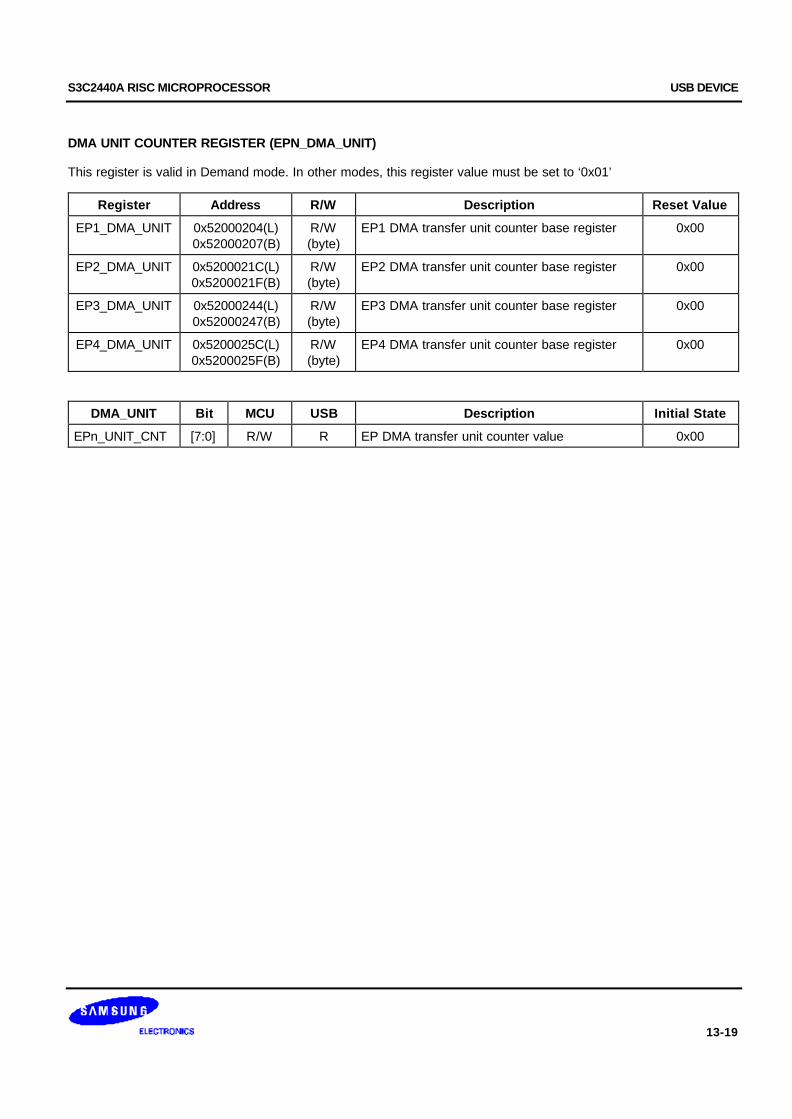
S3C2440A RISC MICROPROCESSOR USB DEVICE
13-19
DMA UNIT COUNTER REGISTER (EPN_DMA_UNIT)
This register is valid in Demand mode. In other modes, this register value must be set to ‘0x01’
Register Address R/W Description Reset Value
EP1_DMA_UNIT 0x52000204(L)0x52000207(B)
R/W(byte)
EP1 DMA transfer unit counter base register 0x00
EP2_DMA_UNIT 0x5200021C(L)0x5200021F(B)
R/W(byte)
EP2 DMA transfer unit counter base register 0x00
EP3_DMA_UNIT 0x52000244(L)0x52000247(B)
R/W(byte)
EP3 DMA transfer unit counter base register 0x00
EP4_DMA_UNIT 0x5200025C(L)0x5200025F(B)
R/W(byte)
EP4 DMA transfer unit counter base register 0x00
DMA_UNIT Bit MCU USB Description Initial State
EPn_UNIT_CNT [7:0] R/W R EP DMA transfer unit counter value 0x00
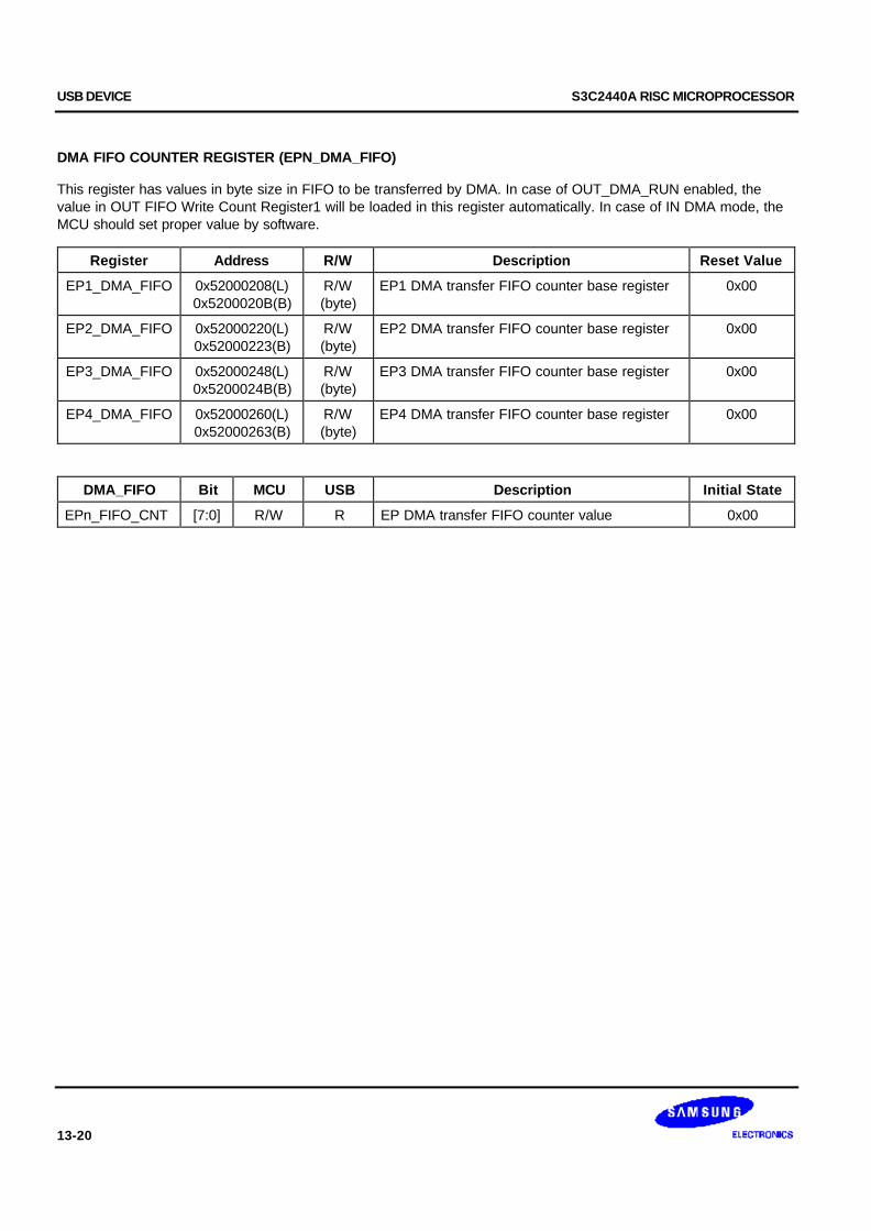
USB DEVICE S3C2440A RISC MICROPROCESSOR
13-20
DMA FIFO COUNTER REGISTER (EPN_DMA_FIFO)
This register has values in byte size in FIFO to be transferred by DMA. In case of OUT_DMA_RUN enabled, thevalue in OUT FIFO Write Count Register1 will be loaded in this register automatically. In case of IN DMA mode, theMCU should set proper value by software.
Register Address R/W Description Reset Value
EP1_DMA_FIFO 0x52000208(L)0x5200020B(B)
R/W(byte)
EP1 DMA transfer FIFO counter base register 0x00
EP2_DMA_FIFO 0x52000220(L)0x52000223(B)
R/W(byte)
EP2 DMA transfer FIFO counter base register 0x00
EP3_DMA_FIFO 0x52000248(L)0x5200024B(B)
R/W(byte)
EP3 DMA transfer FIFO counter base register 0x00
EP4_DMA_FIFO 0x52000260(L)0x52000263(B)
R/W(byte)
EP4 DMA transfer FIFO counter base register 0x00
DMA_FIFO Bit MCU USB Description Initial State
EPn_FIFO_CNT [7:0] R/W R EP DMA transfer FIFO counter value 0x00
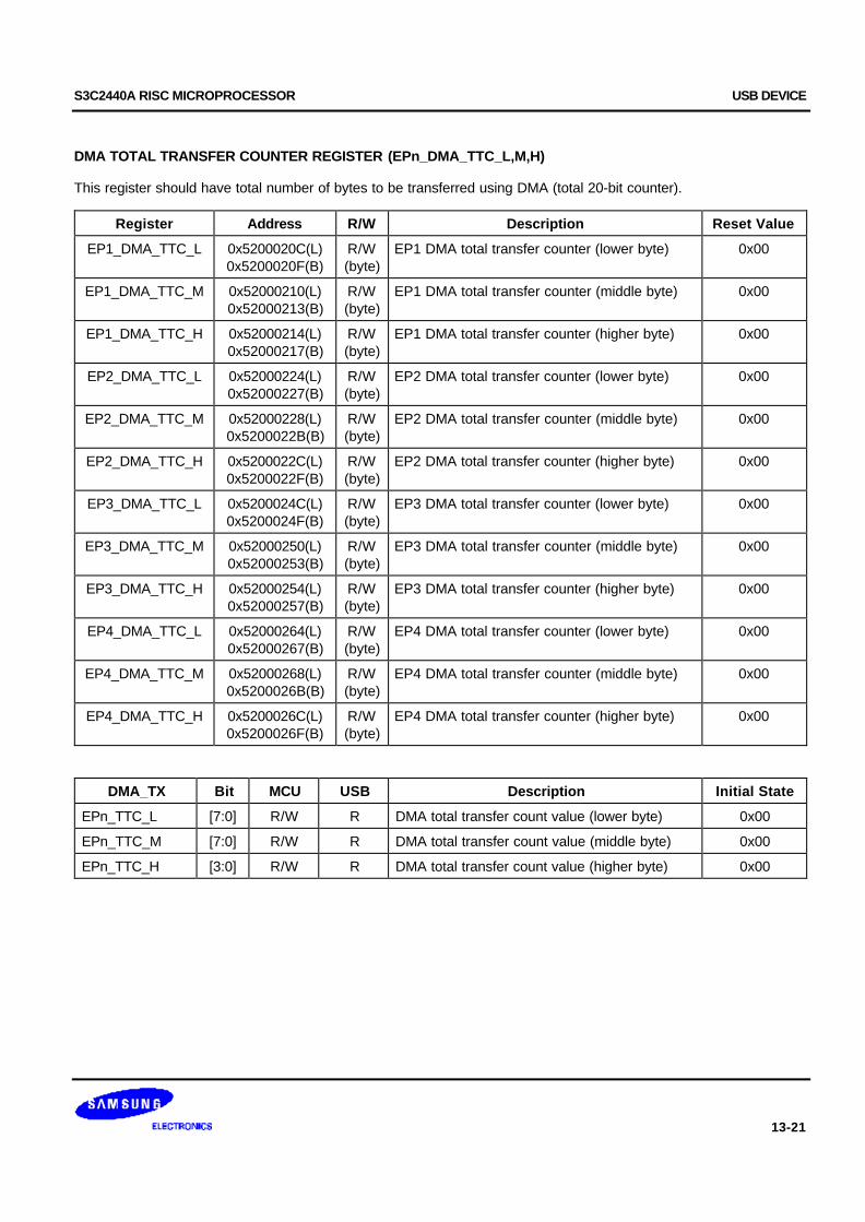
S3C2440A RISC MICROPROCESSOR USB DEVICE
13-21
DMA TOTAL TRANSFER COUNTER REGISTER (EPn_DMA_TTC_L,M,H)
This register should have total number of bytes to be transferred using DMA (total 20-bit counter).
Register Address R/W Description Reset Value
EP1_DMA_TTC_L 0x5200020C(L)0x5200020F(B)
R/W(byte)
EP1 DMA total transfer counter (lower byte) 0x00
EP1_DMA_TTC_M 0x52000210(L)0x52000213(B)
R/W(byte)
EP1 DMA total transfer counter (middle byte) 0x00
EP1_DMA_TTC_H 0x52000214(L)0x52000217(B)
R/W(byte)
EP1 DMA total transfer counter (higher byte) 0x00
EP2_DMA_TTC_L 0x52000224(L)0x52000227(B)
R/W(byte)
EP2 DMA total transfer counter (lower byte) 0x00
EP2_DMA_TTC_M 0x52000228(L)0x5200022B(B)
R/W(byte)
EP2 DMA total transfer counter (middle byte) 0x00
EP2_DMA_TTC_H 0x5200022C(L)0x5200022F(B)
R/W(byte)
EP2 DMA total transfer counter (higher byte) 0x00
EP3_DMA_TTC_L 0x5200024C(L)0x5200024F(B)
R/W(byte)
EP3 DMA total transfer counter (lower byte) 0x00
EP3_DMA_TTC_M 0x52000250(L)0x52000253(B)
R/W(byte)
EP3 DMA total transfer counter (middle byte) 0x00
EP3_DMA_TTC_H 0x52000254(L)0x52000257(B)
R/W(byte)
EP3 DMA total transfer counter (higher byte) 0x00
EP4_DMA_TTC_L 0x52000264(L)0x52000267(B)
R/W(byte)
EP4 DMA total transfer counter (lower byte) 0x00
EP4_DMA_TTC_M 0x52000268(L)0x5200026B(B)
R/W(byte)
EP4 DMA total transfer counter (middle byte) 0x00
EP4_DMA_TTC_H 0x5200026C(L)0x5200026F(B)
R/W(byte)
EP4 DMA total transfer counter (higher byte) 0x00
DMA_TX Bit MCU USB Description Initial State
EPn_TTC_L [7:0] R/W R DMA total transfer count value (lower byte) 0x00
EPn_TTC_M [7:0] R/W R DMA total transfer count value (middle byte) 0x00
EPn_TTC_H [3:0] R/W R DMA total transfer count value (higher byte) 0x00

USB DEVICE S3C2440A RISC MICROPROCESSOR
13-22
NOTES

S3C2440A RISC MICROPROCESSOR INTERRUPT CONTROLLER
14-1
14 INTERRUPT CONTROLLER
OVERVIEW
The interrupt controller in the S3C2440A receives the request from 60 interrupt sources. These interrupt sources areprovided by internal peripherals such as DMA controller, UART, IIC, and others. In these interrupt sources, theUARTn, AC97 and EINTn interrupts are 'OR'ed to the interrupt controller.
When receiving multiple interrupt requests from internal peripherals and external interrupt request pins, the interruptcontroller requests FIQ or IRQ interrupt of the ARM920T core after the arbitration procedure.
The arbitration procedure depends on the hardware priority logic and the result is written to the interrupt pendingregister, which helps users notify which interrupt is generated out of various interrupt sources.
Request sources(with sub -register)
Request sources(without sub -register)
SRCPND MASK
MODE
Priority
INTPND
IRQ
FIQ
SUBSRCPND SUBMASK
LCD interrupt has different features. Please see the chapter 15 LCD Controller
Figure 14-1. Interrupt Process Diagram
INTERRUPT CONTROLLER S3C2440A RISC MICROPROCESSOR
14-2
INTERRUPT CONTROLLER OPERATION
F-bit and I-bit of Program Status Register (PSR)
If the F-bit of PSR in ARM920T CPU is set to 1, the CPU does not accept the Fast Interrupt Request (FIQ) from theinterrupt controller. Likewise, If I-bit of the PSR is set to 1, the CPU does not accept the Interrupt Request (IRQ) fromthe interrupt controller. So, the interrupt controller can receive interrupts by clearing F-bit or I-bit of the PSR to 0 andsetting the corresponding bit of INTMSK to 0.
Interrupt Mode
The ARM920T has two types of Interrupt mode: FIQ or IRQ. All the interrupt sources determine which mode is usedat interrupt request.
Interrupt Pending Register
The S3C2440A has two interrupt pending registers: source pending register (SRCPND) and interrupt pending register(INTPND). These pending registers indicate whether an interrupt request is pending or not. When the interruptsources request interrupt the service, the corresponding bits of SRCPND register are set to 1, and at the same time,only one bit of the INTPND register is set to 1 automatically after arbitration procedure. If interrupts are masked, thenthe corresponding bits of the SRCPND register are set to 1. This does not cause the bit of INTPND register changed.When a pending bit of INTPND register is set, the interrupt service routine will start whenever the I-flag or F-flag iscleared to 0. The SRCPND and INTPND registers can be read and written, so the service routine must clear thepending condition by writing a 1 to the corresponding bit in the SRCPND register first and then clear the pendingcondition in the INTPND registers by using the same method.
Interrupt Mask Register
This register indicates that an interrupt has been disabled if the corresponding mask bit is set to 1. If an interruptmask bit of INTMSK is 0, the interrupt will be serviced normally. If the corresponding mask bit is 1 and the interrupt isgenerated, the source pending bit will be set.
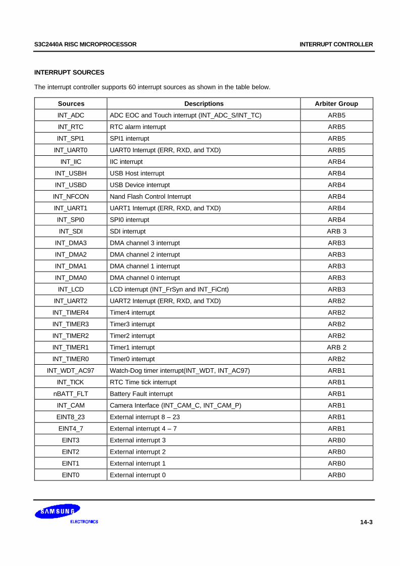
S3C2440A RISC MICROPROCESSOR INTERRUPT CONTROLLER
14-3
INTERRUPT SOURCES
The interrupt controller supports 60 interrupt sources as shown in the table below.
Sources Descriptions Arbiter Group
INT_ADC ADC EOC and Touch interrupt (INT_ADC_S/INT_TC) ARB5
INT_RTC RTC alarm interrupt ARB5
INT_SPI1 SPI1 interrupt ARB5
INT_UART0 UART0 Interrupt (ERR, RXD, and TXD) ARB5
INT_IIC IIC interrupt ARB4
INT_USBH USB Host interrupt ARB4
INT_USBD USB Device interrupt ARB4
INT_NFCON Nand Flash Control Interrupt ARB4
INT_UART1 UART1 Interrupt (ERR, RXD, and TXD) ARB4
INT_SPI0 SPI0 interrupt ARB4
INT_SDI SDI interrupt ARB 3
INT_DMA3 DMA channel 3 interrupt ARB3
INT_DMA2 DMA channel 2 interrupt ARB3
INT_DMA1 DMA channel 1 interrupt ARB3
INT_DMA0 DMA channel 0 interrupt ARB3
INT_LCD LCD interrupt (INT_FrSyn and INT_FiCnt) ARB3
INT_UART2 UART2 Interrupt (ERR, RXD, and TXD) ARB2
INT_TIMER4 Timer4 interrupt ARB2
INT_TIMER3 Timer3 interrupt ARB2
INT_TIMER2 Timer2 interrupt ARB2
INT_TIMER1 Timer1 interrupt ARB 2
INT_TIMER0 Timer0 interrupt ARB2
INT_WDT_AC97 Watch-Dog timer interrupt(INT_WDT, INT_AC97) ARB1
INT_TICK RTC Time tick interrupt ARB1
nBATT_FLT Battery Fault interrupt ARB1
INT_CAM Camera Interface (INT_CAM_C, INT_CAM_P) ARB1
EINT8_23 External interrupt 8 – 23 ARB1
EINT4_7 External interrupt 4 – 7 ARB1
EINT3 External interrupt 3 ARB0
EINT2 External interrupt 2 ARB0
EINT1 External interrupt 1 ARB0
EINT0 External interrupt 0 ARB0

INTERRUPT CONTROLLER S3C2440A RISC MICROPROCESSOR
14-4
INTERRUPT SUB SOURCES
Sub Sources Descriptions Source
INT_AC97 AC97 interrupt INT_WDT_AC97
INT_WDT Watchdoc interrupt INT_WDT_AC97
INT_CAM_P P-port capture interrupt in camera interface INT_CAM
INT_CAM_C C-port capture interrupt in camera interface INT_CAM
INT_ADC_S ADC interrupt INT_ADC
INT_TC Touch screen interrupt (pen up/down) INT_ADC
INT_ERR2 UART2 error interrupt INT_UART2
INT_TXD2 UART2 transmit interrupt INT_UART2
INT_RXD2 UART2 receive interrupt INT_UART2
INT_ERR1 UART1 error interrupt INT_UART1
INT_TXD1 UART1 transmit interrupt INT_UART1
INT_RXD1 UART1 receive interrupt INT_UART1
INT_ERR0 UART0 error interrupt INT_UART0
INT_TXD0 UART0 transmit interrupt INT_UART0
INT_RXD0 UART0 receive interrupt INT_UART0
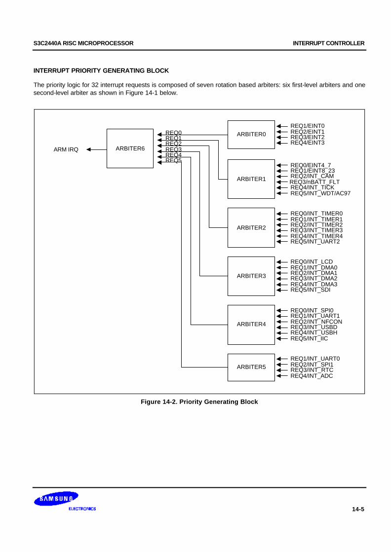
S3C2440A RISC MICROPROCESSOR INTERRUPT CONTROLLER
14-5
INTERRUPT PRIORITY GENERATING BLOCK
The priority logic for 32 interrupt requests is composed of seven rotation based arbiters: six first-level arbiters and onesecond-level arbiter as shown in Figure 14-1 below.
ARBITER6
ARBITER0
ARM IRQ
REQ1/EINT0
ARBITER1
ARBITER2
ARBITER3
ARBITER4
ARBITER5
REQ4/INT_TICKREQ5/INT_WDT/AC97
REQ0/INT_TIMER0
REQ3/INT_TIMER3REQ2/INT_TIMER2REQ1/INT_TIMER1
REQ4/INT_TIMER4
REQ0/INT_LCDREQ1/INT_DMA0
REQ3/INT_DMA2REQ2/INT_DMA1
REQ5/INT_UART2
REQ4/INT_DMA3REQ5/INT_SDI
REQ0/INT_SPI0REQ1/INT_UART1REQ2/INT_NFCONREQ3/INT_USBDREQ4/INT_USBHREQ5/INT_IIC
REQ1/INT_UART0REQ2/INT_SPI1REQ3/INT_RTCREQ4/INT_ADC
REQ0REQ1REQ2REQ3REQ4REQ5
REQ2/EINT1REQ3/EINT2REQ4/EINT3
REQ0/EINT4_7REQ1/EINT8_23REQ2/INT_CAMREQ3/nBATT_FLT
Figure 14-2. Priority Generating Block
INTERRUPT CONTROLLER S3C2440A RISC MICROPROCESSOR
14-6
INTERRUPT PRIORITY
Each arbiter can handle six interrupt requests based on the one bit arbiter mode control (ARB_MODE) and two bitsof selection control signals (ARB_SEL) as follows:
— If ARB_SEL bits are 00b, the priority order is REQ0, REQ1, REQ2, REQ3, REQ4, and REQ5.
— If ARB_SEL bits are 01b, the priority order is REQ0, REQ2, REQ3, REQ4, REQ1, and REQ5.
— If ARB_SEL bits are 10b, the priority order is REQ0, REQ3, REQ4, REQ1, REQ2, and REQ5.
— If ARB_SEL bits are 11b, the priority order is REQ0, REQ4, REQ1, REQ2, REQ3, and REQ5.
Note that REQ0 of an arbiter always has the highest priority, and REQ5 has the lowest one. In addition, by changingthe ARB_SEL bits, we can rotate the priority of REQ1 to REQ4.
Here, if ARB_MODE bit is set to 0, ARB_SEL bits doesn’t change automatically changed, making the arbiter tooperate in the fixed priority mode (note that even in this mode, we can reconfigure the priority by manually changingthe ARB_SEL bits). On the other hand, if ARB_MODE bit is 1, ARB_SEL bits are changed in rotation fashion, e.g., ifREQ1 is serviced, ARB_SEL bits are changed to 01b automatically so as to put REQ1 into the lowest priority. Thedetailed rules of ARB_SEL change are as follows:
— If REQ0 or REQ5 is serviced, ARB_SEL bits are not changed at all.
— If REQ1 is serviced, ARB_SEL bits are changed to 01b.
— If REQ2 is serviced, ARB_SEL bits are changed to 10b.
— If REQ3 is serviced, ARB_SEL bits are changed to 11b.
— If REQ4 is serviced, ARB_SEL bits are changed to 00b.

S3C2440A RISC MICROPROCESSOR INTERRUPT CONTROLLER
14-7
INTERRUPT CONTROLLER SPECIAL REGISTERS
There are five control registers in the interrupt controller: source pending register, interrupt mode register, maskregister, priority register, and interrupt pending register.
All the interrupt requests from the interrupt sources are first registered in the source pending register. They aredivided into two groups including Fast Interrupt Request (FIQ) and Interrupt Request (IRQ), based on the interruptmode register. The arbitration procedure for multiple IRQs is based on the priority register.
SOURCE PENDING (SRCPND) REGISTER
The SRCPND register is composed of 32 bits each of which is related to an interrupt source. Each bit is set to 1 ifthe corresponding interrupt source generates the interrupt request and waits for the interrupt to be serviced.Accordingly, this register indicates which interrupt source is waiting for the request to be serviced. Note that each bitof the SRCPND register is automatically set by the interrupt sources regardless of the masking bits in the INTMASKregister. In addition, the SRCPND register is not affected by the priority logic of interrupt controller.
In the interrupt service routine for a specific interrupt source, the corresponding bit of the SRCPND register has to becleared to get the interrupt request from the same source correctly. If you return from the ISR without clearing the bit,the interrupt controller operates as if another interrupt request came in from the same source. In other words, if aspecific bit of the SRCPND register is set to 1, it is always considered as a valid interrupt request waiting to beserviced.
The time to clear the corresponding bit depends on the user's requirement. If you want to receive another validrequest from the same source, you should clear the corresponding bit first, and then enable the interrupt.
You can clear a specific bit of the SRCPND register by writing a data to this register. It clears only the bit positionsof the SRCPND corresponding to those set to one in the data. The bit positions corresponding to those that are setto 0 in the data remains as they are.
Register Address R/W Description Reset Value
SRCPND 0X4A000000 R/W Indicate the interrupt request status.
0 = The interrupt has not been requested.1 = The interrupt source has asserted the interrupt request.
0x00000000
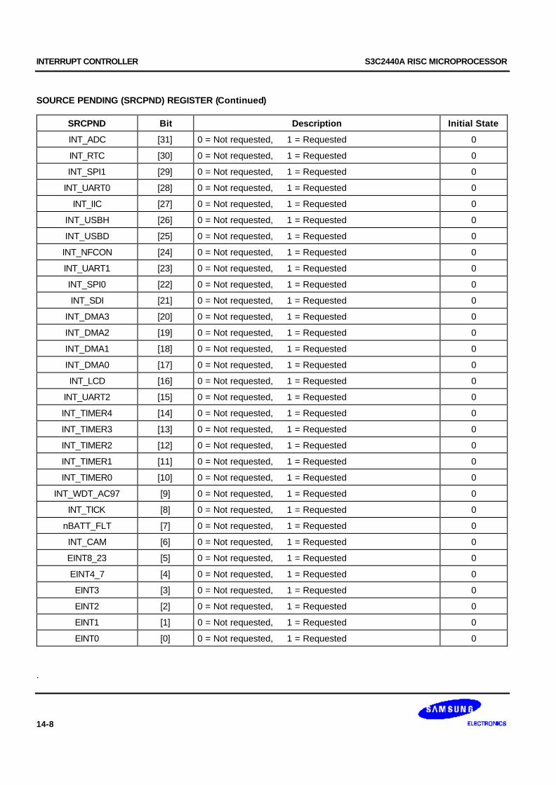
INTERRUPT CONTROLLER S3C2440A RISC MICROPROCESSOR
14-8
SOURCE PENDING (SRCPND) REGISTER (Continued)
SRCPND Bit Description Initial State
INT_ADC [31] 0 = Not requested, 1 = Requested 0
INT_RTC [30] 0 = Not requested, 1 = Requested 0
INT_SPI1 [29] 0 = Not requested, 1 = Requested 0
INT_UART0 [28] 0 = Not requested, 1 = Requested 0
INT_IIC [27] 0 = Not requested, 1 = Requested 0
INT_USBH [26] 0 = Not requested, 1 = Requested 0
INT_USBD [25] 0 = Not requested, 1 = Requested 0
INT_NFCON [24] 0 = Not requested, 1 = Requested 0
INT_UART1 [23] 0 = Not requested, 1 = Requested 0
INT_SPI0 [22] 0 = Not requested, 1 = Requested 0
INT_SDI [21] 0 = Not requested, 1 = Requested 0
INT_DMA3 [20] 0 = Not requested, 1 = Requested 0
INT_DMA2 [19] 0 = Not requested, 1 = Requested 0
INT_DMA1 [18] 0 = Not requested, 1 = Requested 0
INT_DMA0 [17] 0 = Not requested, 1 = Requested 0
INT_LCD [16] 0 = Not requested, 1 = Requested 0
INT_UART2 [15] 0 = Not requested, 1 = Requested 0
INT_TIMER4 [14] 0 = Not requested, 1 = Requested 0
INT_TIMER3 [13] 0 = Not requested, 1 = Requested 0
INT_TIMER2 [12] 0 = Not requested, 1 = Requested 0
INT_TIMER1 [11] 0 = Not requested, 1 = Requested 0
INT_TIMER0 [10] 0 = Not requested, 1 = Requested 0
INT_WDT_AC97 [9] 0 = Not requested, 1 = Requested 0
INT_TICK [8] 0 = Not requested, 1 = Requested 0
nBATT_FLT [7] 0 = Not requested, 1 = Requested 0
INT_CAM [6] 0 = Not requested, 1 = Requested 0
EINT8_23 [5] 0 = Not requested, 1 = Requested 0
EINT4_7 [4] 0 = Not requested, 1 = Requested 0
EINT3 [3] 0 = Not requested, 1 = Requested 0
EINT2 [2] 0 = Not requested, 1 = Requested 0
EINT1 [1] 0 = Not requested, 1 = Requested 0
EINT0 [0] 0 = Not requested, 1 = Requested 0
.
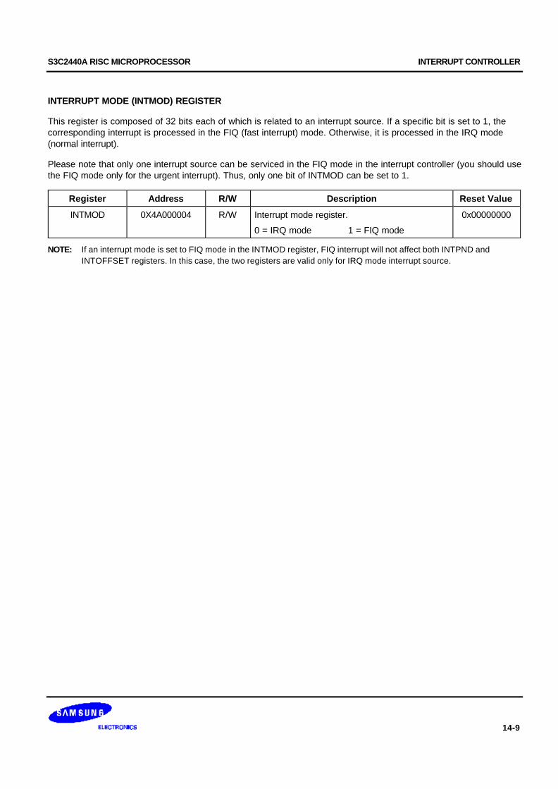
S3C2440A RISC MICROPROCESSOR INTERRUPT CONTROLLER
14-9
INTERRUPT MODE (INTMOD) REGISTER
This register is composed of 32 bits each of which is related to an interrupt source. If a specific bit is set to 1, thecorresponding interrupt is processed in the FIQ (fast interrupt) mode. Otherwise, it is processed in the IRQ mode(normal interrupt).
Please note that only one interrupt source can be serviced in the FIQ mode in the interrupt controller (you should usethe FIQ mode only for the urgent interrupt). Thus, only one bit of INTMOD can be set to 1.
Register Address R/W Description Reset Value
INTMOD 0X4A000004 R/W Interrupt mode register.
0 = IRQ mode 1 = FIQ mode
0x00000000
NOTE: If an interrupt mode is set to FIQ mode in the INTMOD register, FIQ interrupt will not affect both INTPND and INTOFFSET registers. In this case, the two registers are valid only for IRQ mode interrupt source.
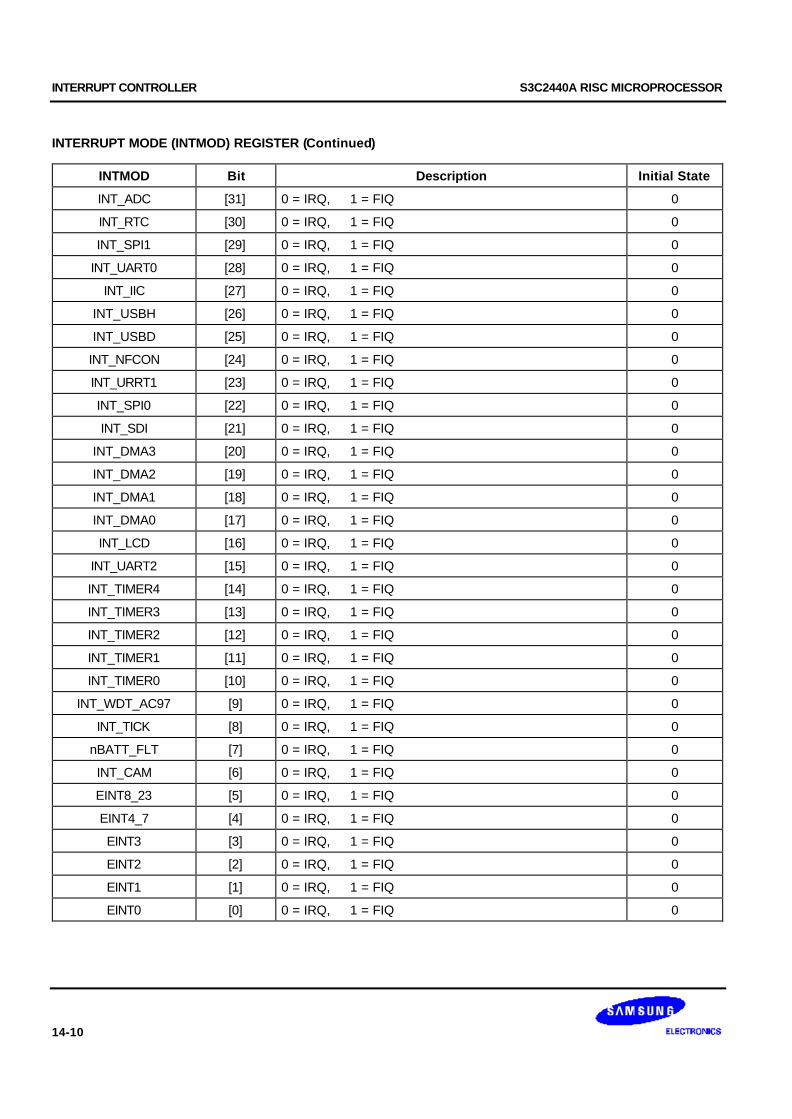
INTERRUPT CONTROLLER S3C2440A RISC MICROPROCESSOR
14-10
INTERRUPT MODE (INTMOD) REGISTER (Continued)
INTMOD Bit Description Initial State
INT_ADC [31] 0 = IRQ, 1 = FIQ 0
INT_RTC [30] 0 = IRQ, 1 = FIQ 0
INT_SPI1 [29] 0 = IRQ, 1 = FIQ 0
INT_UART0 [28] 0 = IRQ, 1 = FIQ 0
INT_IIC [27] 0 = IRQ, 1 = FIQ 0
INT_USBH [26] 0 = IRQ, 1 = FIQ 0
INT_USBD [25] 0 = IRQ, 1 = FIQ 0
INT_NFCON [24] 0 = IRQ, 1 = FIQ 0
INT_URRT1 [23] 0 = IRQ, 1 = FIQ 0
INT_SPI0 [22] 0 = IRQ, 1 = FIQ 0
INT_SDI [21] 0 = IRQ, 1 = FIQ 0
INT_DMA3 [20] 0 = IRQ, 1 = FIQ 0
INT_DMA2 [19] 0 = IRQ, 1 = FIQ 0
INT_DMA1 [18] 0 = IRQ, 1 = FIQ 0
INT_DMA0 [17] 0 = IRQ, 1 = FIQ 0
INT_LCD [16] 0 = IRQ, 1 = FIQ 0
INT_UART2 [15] 0 = IRQ, 1 = FIQ 0
INT_TIMER4 [14] 0 = IRQ, 1 = FIQ 0
INT_TIMER3 [13] 0 = IRQ, 1 = FIQ 0
INT_TIMER2 [12] 0 = IRQ, 1 = FIQ 0
INT_TIMER1 [11] 0 = IRQ, 1 = FIQ 0
INT_TIMER0 [10] 0 = IRQ, 1 = FIQ 0
INT_WDT_AC97 [9] 0 = IRQ, 1 = FIQ 0
INT_TICK [8] 0 = IRQ, 1 = FIQ 0
nBATT_FLT [7] 0 = IRQ, 1 = FIQ 0
INT_CAM [6] 0 = IRQ, 1 = FIQ 0
EINT8_23 [5] 0 = IRQ, 1 = FIQ 0
EINT4_7 [4] 0 = IRQ, 1 = FIQ 0
EINT3 [3] 0 = IRQ, 1 = FIQ 0
EINT2 [2] 0 = IRQ, 1 = FIQ 0
EINT1 [1] 0 = IRQ, 1 = FIQ 0
EINT0 [0] 0 = IRQ, 1 = FIQ 0
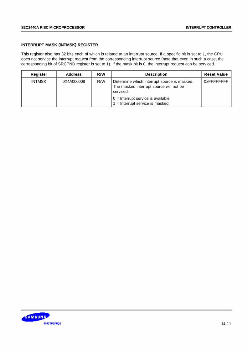
S3C2440A RISC MICROPROCESSOR INTERRUPT CONTROLLER
14-11
INTERRUPT MASK (INTMSK) REGISTER
This register also has 32 bits each of which is related to an interrupt source. If a specific bit is set to 1, the CPUdoes not service the interrupt request from the corresponding interrupt source (note that even in such a case, thecorresponding bit of SRCPND register is set to 1). If the mask bit is 0, the interrupt request can be serviced.
Register Address R/W Description Reset Value
INTMSK 0X4A000008 R/W Determine which interrupt source is masked.The masked interrupt source will not beserviced.
0 = Interrupt service is available.1 = Interrupt service is masked.
0xFFFFFFFF

INTERRUPT CONTROLLER S3C2440A RISC MICROPROCESSOR
14-12
INTERRUPT MASK (INTMSK) REGISTER (Continued)
INTMSK Bit Description Initial State
INT_ADC [31] 0 = Service available, 1 = Masked 1
INT_RTC [30] 0 = Service available, 1 = Masked 1
INT_SPI1 [29] 0 = Service available, 1 = Masked 1
INT_UART0 [28] 0 = Service available, 1 = Masked 1
INT_IIC [27] 0 = Service available, 1 = Masked 1
INT_USBH [26] 0 = Service available, 1 = Masked 1
INT_USBD [25] 0 = Service available, 1 = Masked 1
INT_NFCON [24] 0 = Service available, 1 = Masked 1
INT_UART1 [23] 0 = Service available, 1 = Masked 1
INT_SPI0 [22] 0 = Service available, 1 = Masked 1
INT_SDI [21] 0 = Service available, 1 = Masked 1
INT_DMA3 [20] 0 = Service available, 1 = Masked 1
INT_DMA2 [19] 0 = Service available, 1 = Masked 1
INT_DMA1 [18] 0 = Service available, 1 = Masked 1
INT_DMA0 [17] 0 = Service available, 1 = Masked 1
INT_LCD [16] 0 = Service available, 1 = Masked 1
INT_UART2 [15] 0 = Service available, 1 = Masked 1
INT_TIMER4 [14] 0 = Service available, 1 = Masked 1
INT_TIMER3 [13] 0 = Service available, 1 = Masked 1
INT_TIMER2 [12] 0 = Service available, 1 = Masked 1
INT_TIMER1 [11] 0 = Service available, 1 = Masked 1
INT_TIMER0 [10] 0 = Service available, 1 = Masked 1
INT_WDT_AC97 [9] 0 = Service available, 1 = Masked 1
INT_TICK [8] 0 = Service available, 1 = Masked 1
nBATT_FLT [7] 0 = Service available, 1 = Masked 1
INT_CAM [6] 0 = Service available, 1 = Masked 1
EINT8_23 [5] 0 = Service available, 1 = Masked 1
EINT4_7 [4] 0 = Service available, 1 = Masked 1
EINT3 [3] 0 = Service available, 1 = Masked 1
EINT2 [2] 0 = Service available, 1 = Masked 1
EINT1 [1] 0 = Service available, 1 = Masked 1
EINT0 [0] 0 = Service available, 1 = Masked 1
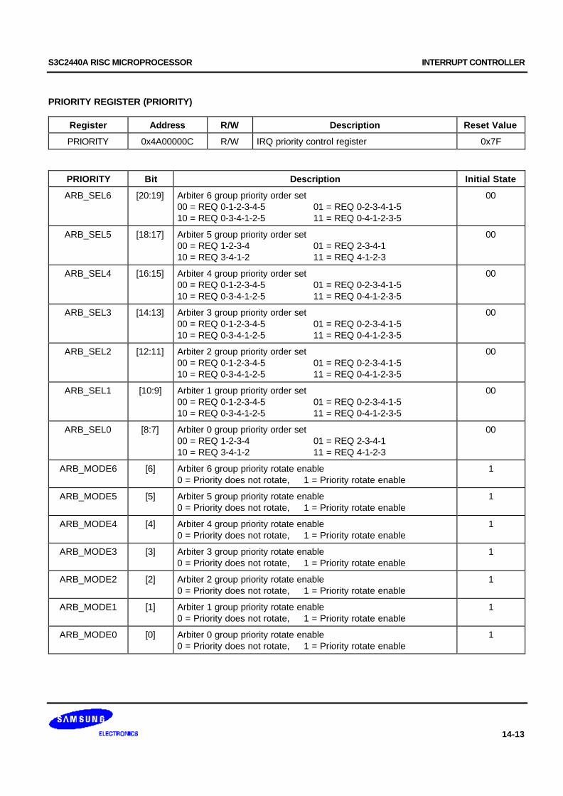
S3C2440A RISC MICROPROCESSOR INTERRUPT CONTROLLER
14-13
PRIORITY REGISTER (PRIORITY)
Register Address R/W Description Reset Value
PRIORITY 0x4A00000C R/W IRQ priority control register 0x7F
PRIORITY Bit Description Initial State
ARB_SEL6 [20:19] Arbiter 6 group priority order set00 = REQ 0-1-2-3-4-5 01 = REQ 0-2-3-4-1-510 = REQ 0-3-4-1-2-5 11 = REQ 0-4-1-2-3-5
00
ARB_SEL5 [18:17] Arbiter 5 group priority order set00 = REQ 1-2-3-4 01 = REQ 2-3-4-110 = REQ 3-4-1-2 11 = REQ 4-1-2-3
00
ARB_SEL4 [16:15] Arbiter 4 group priority order set00 = REQ 0-1-2-3-4-5 01 = REQ 0-2-3-4-1-510 = REQ 0-3-4-1-2-5 11 = REQ 0-4-1-2-3-5
00
ARB_SEL3 [14:13] Arbiter 3 group priority order set00 = REQ 0-1-2-3-4-5 01 = REQ 0-2-3-4-1-510 = REQ 0-3-4-1-2-5 11 = REQ 0-4-1-2-3-5
00
ARB_SEL2 [12:11] Arbiter 2 group priority order set00 = REQ 0-1-2-3-4-5 01 = REQ 0-2-3-4-1-510 = REQ 0-3-4-1-2-5 11 = REQ 0-4-1-2-3-5
00
ARB_SEL1 [10:9] Arbiter 1 group priority order set00 = REQ 0-1-2-3-4-5 01 = REQ 0-2-3-4-1-510 = REQ 0-3-4-1-2-5 11 = REQ 0-4-1-2-3-5
00
ARB_SEL0 [8:7] Arbiter 0 group priority order set00 = REQ 1-2-3-4 01 = REQ 2-3-4-110 = REQ 3-4-1-2 11 = REQ 4-1-2-3
00
ARB_MODE6 [6] Arbiter 6 group priority rotate enable0 = Priority does not rotate, 1 = Priority rotate enable
1
ARB_MODE5 [5] Arbiter 5 group priority rotate enable0 = Priority does not rotate, 1 = Priority rotate enable
1
ARB_MODE4 [4] Arbiter 4 group priority rotate enable0 = Priority does not rotate, 1 = Priority rotate enable
1
ARB_MODE3 [3] Arbiter 3 group priority rotate enable0 = Priority does not rotate, 1 = Priority rotate enable
1
ARB_MODE2 [2] Arbiter 2 group priority rotate enable0 = Priority does not rotate, 1 = Priority rotate enable
1
ARB_MODE1 [1] Arbiter 1 group priority rotate enable0 = Priority does not rotate, 1 = Priority rotate enable
1
ARB_MODE0 [0] Arbiter 0 group priority rotate enable0 = Priority does not rotate, 1 = Priority rotate enable
1
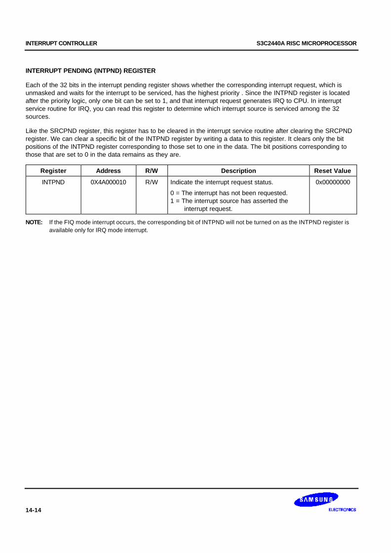
INTERRUPT CONTROLLER S3C2440A RISC MICROPROCESSOR
14-14
INTERRUPT PENDING (INTPND) REGISTER
Each of the 32 bits in the interrupt pending register shows whether the corresponding interrupt request, which isunmasked and waits for the interrupt to be serviced, has the highest priority . Since the INTPND register is locatedafter the priority logic, only one bit can be set to 1, and that interrupt request generates IRQ to CPU. In interruptservice routine for IRQ, you can read this register to determine which interrupt source is serviced among the 32sources.
Like the SRCPND register, this register has to be cleared in the interrupt service routine after clearing the SRCPNDregister. We can clear a specific bit of the INTPND register by writing a data to this register. It clears only the bitpositions of the INTPND register corresponding to those set to one in the data. The bit positions corresponding tothose that are set to 0 in the data remains as they are.
Register Address R/W Description Reset Value
INTPND 0X4A000010 R/W Indicate the interrupt request status.
0 = The interrupt has not been requested.1 = The interrupt source has asserted the interrupt request.
0x00000000
NOTE: If the FIQ mode interrupt occurs, the corresponding bit of INTPND will not be turned on as the INTPND register isavailable only for IRQ mode interrupt.
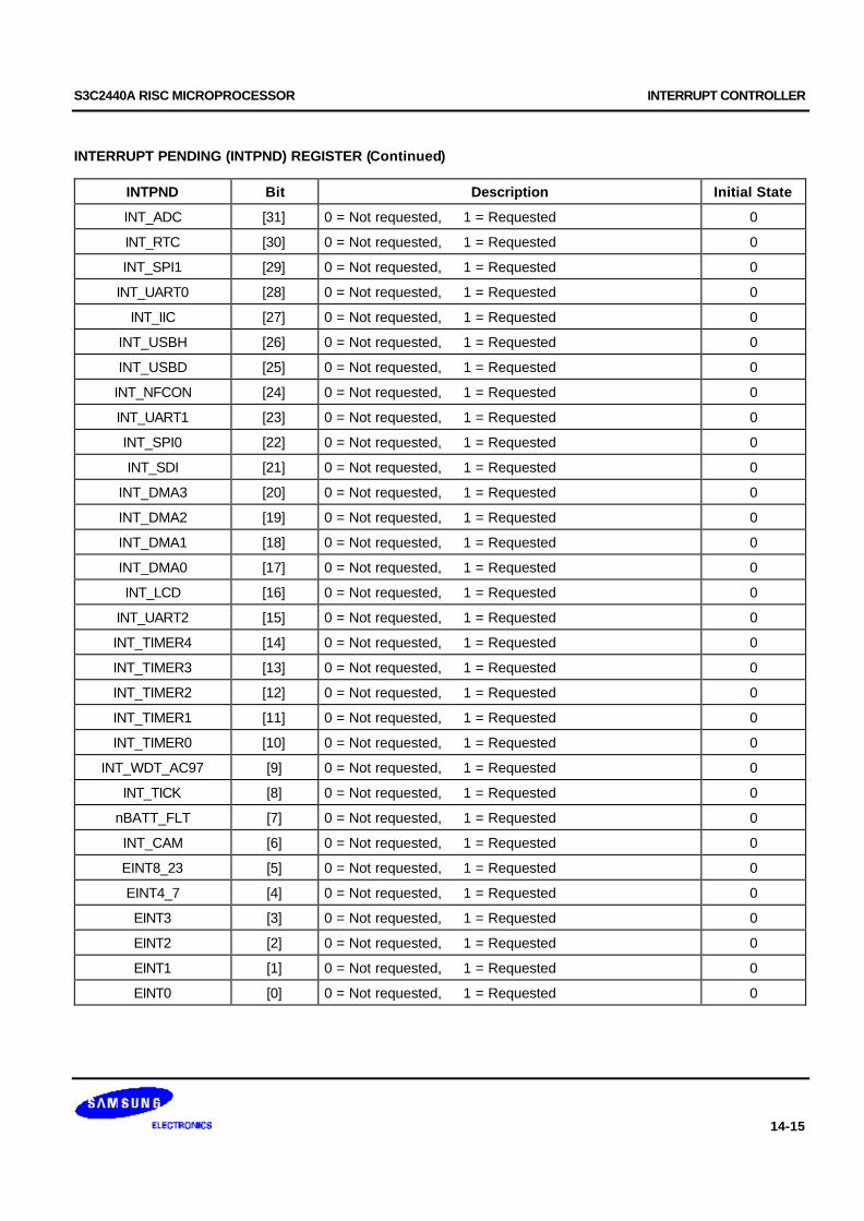
S3C2440A RISC MICROPROCESSOR INTERRUPT CONTROLLER
14-15
INTERRUPT PENDING (INTPND) REGISTER (Continued)
INTPND Bit Description Initial State
INT_ADC [31] 0 = Not requested, 1 = Requested 0
INT_RTC [30] 0 = Not requested, 1 = Requested 0
INT_SPI1 [29] 0 = Not requested, 1 = Requested 0
INT_UART0 [28] 0 = Not requested, 1 = Requested 0
INT_IIC [27] 0 = Not requested, 1 = Requested 0
INT_USBH [26] 0 = Not requested, 1 = Requested 0
INT_USBD [25] 0 = Not requested, 1 = Requested 0
INT_NFCON [24] 0 = Not requested, 1 = Requested 0
INT_UART1 [23] 0 = Not requested, 1 = Requested 0
INT_SPI0 [22] 0 = Not requested, 1 = Requested 0
INT_SDI [21] 0 = Not requested, 1 = Requested 0
INT_DMA3 [20] 0 = Not requested, 1 = Requested 0
INT_DMA2 [19] 0 = Not requested, 1 = Requested 0
INT_DMA1 [18] 0 = Not requested, 1 = Requested 0
INT_DMA0 [17] 0 = Not requested, 1 = Requested 0
INT_LCD [16] 0 = Not requested, 1 = Requested 0
INT_UART2 [15] 0 = Not requested, 1 = Requested 0
INT_TIMER4 [14] 0 = Not requested, 1 = Requested 0
INT_TIMER3 [13] 0 = Not requested, 1 = Requested 0
INT_TIMER2 [12] 0 = Not requested, 1 = Requested 0
INT_TIMER1 [11] 0 = Not requested, 1 = Requested 0
INT_TIMER0 [10] 0 = Not requested, 1 = Requested 0
INT_WDT_AC97 [9] 0 = Not requested, 1 = Requested 0
INT_TICK [8] 0 = Not requested, 1 = Requested 0
nBATT_FLT [7] 0 = Not requested, 1 = Requested 0
INT_CAM [6] 0 = Not requested, 1 = Requested 0
EINT8_23 [5] 0 = Not requested, 1 = Requested 0
EINT4_7 [4] 0 = Not requested, 1 = Requested 0
EINT3 [3] 0 = Not requested, 1 = Requested 0
EINT2 [2] 0 = Not requested, 1 = Requested 0
EINT1 [1] 0 = Not requested, 1 = Requested 0
EINT0 [0] 0 = Not requested, 1 = Requested 0
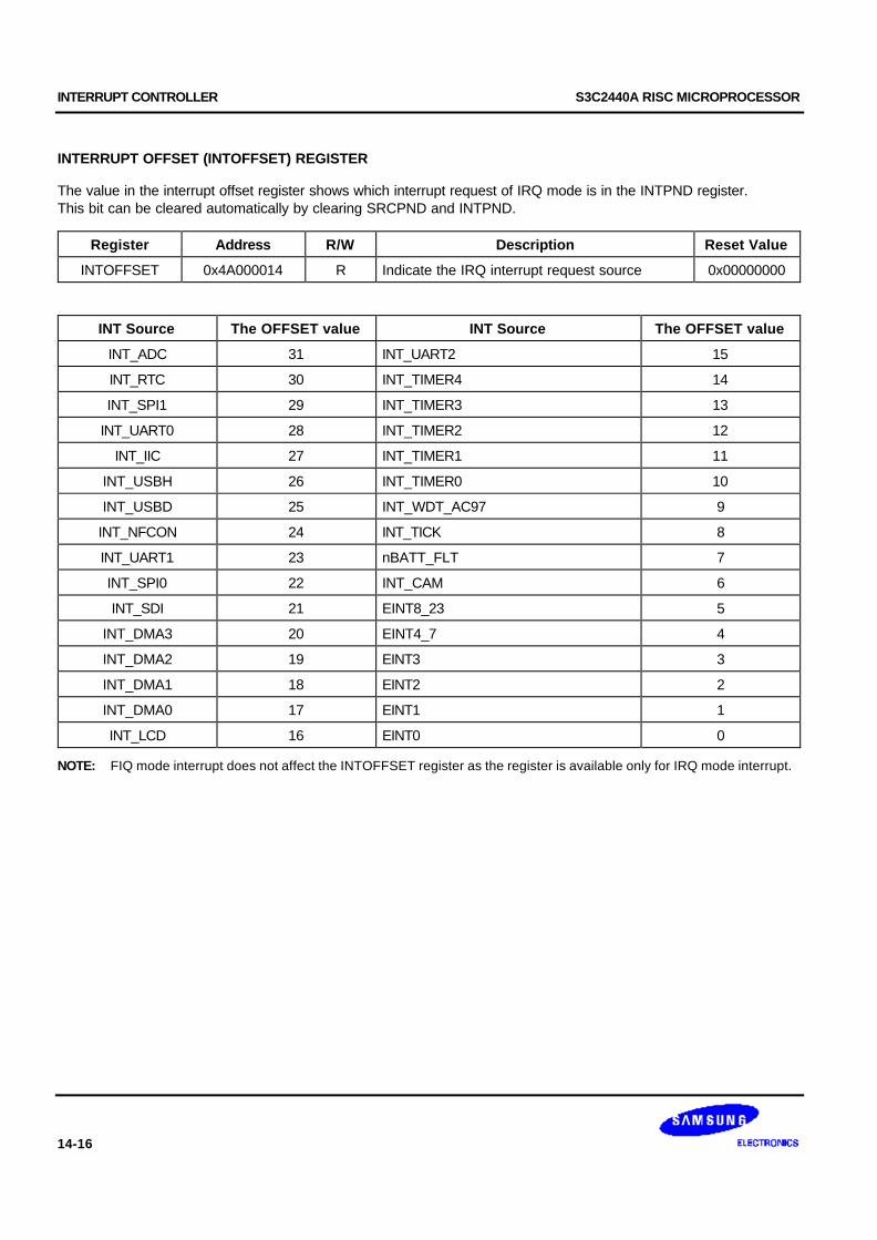
INTERRUPT CONTROLLER S3C2440A RISC MICROPROCESSOR
14-16
INTERRUPT OFFSET (INTOFFSET) REGISTER
The value in the interrupt offset register shows which interrupt request of IRQ mode is in the INTPND register.This bit can be cleared automatically by clearing SRCPND and INTPND.
Register Address R/W Description Reset Value
INTOFFSET 0x4A000014 R Indicate the IRQ interrupt request source 0x00000000
INT Source The OFFSET value INT Source The OFFSET value
INT_ADC 31 INT_UART2 15
INT_RTC 30 INT_TIMER4 14
INT_SPI1 29 INT_TIMER3 13
INT_UART0 28 INT_TIMER2 12
INT_IIC 27 INT_TIMER1 11
INT_USBH 26 INT_TIMER0 10
INT_USBD 25 INT_WDT_AC97 9
INT_NFCON 24 INT_TICK 8
INT_UART1 23 nBATT_FLT 7
INT_SPI0 22 INT_CAM 6
INT_SDI 21 EINT8_23 5
INT_DMA3 20 EINT4_7 4
INT_DMA2 19 EINT3 3
INT_DMA1 18 EINT2 2
INT_DMA0 17 EINT1 1
INT_LCD 16 EINT0 0
NOTE: FIQ mode interrupt does not affect the INTOFFSET register as the register is available only for IRQ mode interrupt.
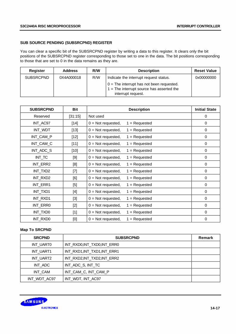
S3C2440A RISC MICROPROCESSOR INTERRUPT CONTROLLER
14-17
SUB SOURCE PENDING (SUBSRCPND) REGISTER
You can clear a specific bit of the SUBSRCPND register by writing a data to this register. It clears only the bitpositions of the SUBSRCPND register corresponding to those set to one in the data. The bit positions correspondingto those that are set to 0 in the data remains as they are.
Register Address R/W Description Reset Value
SUBSRCPND 0X4A000018 R/W Indicate the interrupt request status.
0 = The interrupt has not been requested.1 = The interrupt source has asserted the interrupt request.
0x00000000
SUBSRCPND Bit Description Initial State
Reserved [31:15] Not used 0
INT_AC97 [14] 0 = Not requested, 1 = Requested 0
INT_WDT [13] 0 = Not requested, 1 = Requested 0
INT_CAM_P [12] 0 = Not requested, 1 = Requested 0
INT_CAM_C [11] 0 = Not requested, 1 = Requested 0
INT_ADC_S [10] 0 = Not requested, 1 = Requested 0
INT_TC [9] 0 = Not requested, 1 = Requested 0
INT_ERR2 [8] 0 = Not requested, 1 = Requested 0
INT_TXD2 [7] 0 = Not requested, 1 = Requested 0
INT_RXD2 [6] 0 = Not requested, 1 = Requested 0
INT_ERR1 [5] 0 = Not requested, 1 = Requested 0
INT_TXD1 [4] 0 = Not requested, 1 = Requested 0
INT_RXD1 [3] 0 = Not requested, 1 = Requested 0
INT_ERR0 [2] 0 = Not requested, 1 = Requested 0
INT_TXD0 [1] 0 = Not requested, 1 = Requested 0
INT_RXD0 [0] 0 = Not requested, 1 = Requested 0
Map To SRCPND
SRCPND SUBSRCPND Remark
INT_UART0 INT_RXD0,INT_TXD0,INT_ERR0
INT_UART1 INT_RXD1,INT_TXD1,INT_ERR1
INT_UART2 INT_RXD2,INT_TXD2,INT_ERR2
INT_ADC INT_ADC_S, INT_TC
INT_CAM INT_CAM_C, INT_CAM_P
INT_WDT_AC97 INT_WDT, INT_AC97
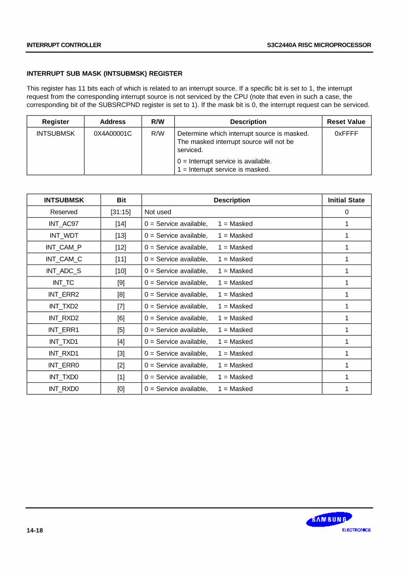
INTERRUPT CONTROLLER S3C2440A RISC MICROPROCESSOR
14-18
INTERRUPT SUB MASK (INTSUBMSK) REGISTER
This register has 11 bits each of which is related to an interrupt source. If a specific bit is set to 1, the interruptrequest from the corresponding interrupt source is not serviced by the CPU (note that even in such a case, thecorresponding bit of the SUBSRCPND register is set to 1). If the mask bit is 0, the interrupt request can be serviced.
Register Address R/W Description Reset Value
INTSUBMSK 0X4A00001C R/W Determine which interrupt source is masked.The masked interrupt source will not beserviced.
0 = Interrupt service is available.1 = Interrupt service is masked.
0xFFFF
INTSUBMSK Bit Description Initial State
Reserved [31:15] Not used 0
INT_AC97 [14] 0 = Service available, 1 = Masked 1
INT_WDT [13] 0 = Service available, 1 = Masked 1
INT_CAM_P [12] 0 = Service available, 1 = Masked 1
INT_CAM_C [11] 0 = Service available, 1 = Masked 1
INT_ADC_S [10] 0 = Service available, 1 = Masked 1
INT_TC [9] 0 = Service available, 1 = Masked 1
INT_ERR2 [8] 0 = Service available, 1 = Masked 1
INT_TXD2 [7] 0 = Service available, 1 = Masked 1
INT_RXD2 [6] 0 = Service available, 1 = Masked 1
INT_ERR1 [5] 0 = Service available, 1 = Masked 1
INT_TXD1 [4] 0 = Service available, 1 = Masked 1
INT_RXD1 [3] 0 = Service available, 1 = Masked 1
INT_ERR0 [2] 0 = Service available, 1 = Masked 1
INT_TXD0 [1] 0 = Service available, 1 = Masked 1
INT_RXD0 [0] 0 = Service available, 1 = Masked 1
S3C2440A RISC MICROPROCESSOR LCD CONTROLLER
15-1
15 LCD CONTROLLER
OVERVIEW
The LCD controller in the S3C2440A consists of the logic for transferring LCD image data from a video buffer locatedin system memory to an external LCD driver.
The LCD controller supports monochrome, 2-bit per pixel (4-level gray scale) or 4-bit per pixel (16-level gray scale)mode on a monochrome LCD, using a time-based dithering algorithm and Frame Rate Control (FRC) method and itcan be interfaced with a color LCD panel at 8-bit per pixel (256-level color) and 12-bit per pixel (4096-level color) forinterfacing with STN LCD.
It can support 1-bit per pixel, 2-bit per pixel, 4-bit per pixel, and 8-bit per pixel for interfacing with the palletized TFTcolor LCD panel, and 16-bit per pixel and 24-bit per pixel for non-palletized true-color display.
The LCD controller can be programmed to support different requirements on the screen related to the number ofhorizontal and vertical pixels, data line width for the data interface, interface timing, and refresh rate.
FEATURES
STN LCD Displays:
— Supports 3 types of LCD panels: 4-bit dual scan, 4-bit single scan, and 8-bit single scan display type
— Supports the monochrome, 4 gray levels, and 16 gray levels
— Supports 256 colors and 4096 colors for color STN LCD panel
— Supports multiple screen sizeTypical actual screen size: 640 x 480, 320 x 240, 160 x 160, and othersMaximum virtual screen size is 4Mbytes.Maximum virtual screen size in 256 color mode: 4096 x 1024, 2048 x 2048, 1024 x 4096, and others
TFT LCD Displays:
— Supports 1, 2, 4 or 8-bpp (bit per pixel) palletized color displays for TFT
— Supports 16, 24-bpp non-palletized true-color displays for color TFT
— Supports maximum 16M color TFT at 24bit per pixel mode
— Supports multiple screen sizeTypical actual screen size: 640 x 480, 320 x 240, 160 x 160, and othersMaximum virtual screen size is 4Mbytes.Maximum virtual screen size in 64K color mode: 2048 x 1024 and others

LCD CONTROLLER S3C2440A RISC MICROPROCESSOR
15-2
COMMON FEATURES
The LCD controller has a dedicated DMA that supports to fetch the image data from video buffer located in systemmemory. Its features also include:
— Dedicated interrupt functions (INT_FrSyn and INT_FiCnt)
— The system memory is used as the display memory.
— Supports Multiple Virtual Display Screen (Supports Hardware Horizontal/Vertical Scrolling)
— Programmable timing control for different display panels
— Supports little and big-endian byte ordering, as well as WinCE data formats
— Supports 2-type SEC TFT LCD panel
(SAMSUNG 3.5” Portrait / 256K Color /Reflective and Transflective a-Si TFT LCD)LTS350Q1-PD1: TFT LCD panel with touch panel and front light unit (Reflective type)LTS350Q1-PD2: TFT LCD panel onlyLTS350Q1-PE1: TFT LCD panel with touch panel and front light unit (Transflective type)LTS350Q1-PE2: TFT LCD panel only
NOTE
WinCE doesn’t support the 12-bit packed data format.Please check if WinCE can support the 12-bit color-mode.
EXTERNAL INTERFACE SIGNAL
STN TFT SEC TFT(LTS350Q1-PD1/2)
SEC TFT(LTS350Q1-PE1/2)
VFRAME(Frame sync. Signal)
VSYNC(Vertical sync. Signal)
STV STV
VLINE(Line sync pulse signal)
HSYNC(Horizontal sync. Signal)
CPV CPV
VCLK(Pixel clock signal)
VCLK(Pixel clock signal)
LCD_HCLK LCD_HCLK
VD[23:0](LCD pixel data output ports)
VD[23:0](LCD pixel data output ports)
VD[23:0] VD[23:0]
VM(AC bias signal for LCD driver)
VDEN(Data enable signal)
TP TP
– LEND(Line end signal)
STH STH
LCD_PWREN LCD_PWREN LCD_PWREN LCD_PWREN
– – LPC_OE LCC_INV
– – LPC_REV LCC_REV
– – LPC_REVB LCC_REVB

S3C2440A RISC MICROPROCESSOR LCD CONTROLLER
15-3
BLOCK DIAGRAM
System Bus
LPC3600 is a timing control logic unit for LTS350Q1-PD1 or LTS350Q1-PD2.LCC3600 is a timing control logic unit for LTS350Q1-PE1 or LTS350Q1-PE2.
REGBANK
LCDCDMAVIDPRCS
LPC3600
TIMEGEN
VD[23:0]
VCLK /LCD_HCLKVLINE / HSYNC / CPVVFRAME / VSYNC / STVVM / VDEN / TP
LCD_LPCOE / LCD_LCCINVLCD_LPCREV / LCD_LCCREVLCD_LPCREVB / LCD_LCCREVB
...VIDEOMUX
LCC3600
Figure 15-1. LCD Controller Block Diagram
The S3C2440A LCD controller is used to transfer the video data and to generate the necessary control signals, suchas VFRAME, VLINE, VCLK, VM, and so on. In addition to the control signals, the S3C2440A has the data ports forvideo data, which are VD[23:0] as shown in Figure 15-1. The LCD controller consists of a REGBANK, LCDCDMA,VIDPRCS, TIMEGEN, and LPC3600 (See the Figure 15-1 LCD Controller Block Diagram). The REGBANK has 17programmable register sets and 256x16 palette memory which are used to configure the LCD controller. TheLCDCDMA is a dedicated DMA, which can transfer the video data in frame memory to LCD driver automatically. Byusing this special DMA, the video data can be displayed on the screen without CPU intervention. The VIDPRCSreceives the video data from the LCDCDMA and sends the video data through the VD[23:0] data ports to the LCDdriver after changing them into a suitable data format, for example 4/8-bit single scan or 4-bit dual scan displaymode. The TIMEGEN consists of programmable logic to support the variable requirements of interface timing andrates commonly found in different LCD drivers. The TIMEGEN block generates VFRAME, VLINE, VCLK, VM, and soon.
The description of data flow is as follows:
FIFO memory is present in the LCDCDMA. When FIFO is empty or partially empty, the LCDCDMA requests datafetching from the frame memory based on the burst memory transfer mode (consecutive memory fetching of 4 words(16 bytes) per one burst request without allowing the bus mastership to another bus master during the bus transfer).When the transfer request is accepted by bus arbitrator in the memory controller, there will be four successive worddata transfers from system memory to internal FIFO. The total size of FIFO is 28 words, which consists of 12 wordsFIFOL and 16 words FIFOH, respectively. The S3C2440A has two FIFOs to support the dual scan display mode. Incase of single scan mode, one of the FIFOs (FIFOH) can only be used.

LCD CONTROLLER S3C2440A RISC MICROPROCESSOR
15-4
STN LCD CONTROLLER OPERATION
TIMING GENERATOR (TIMEGEN)
The TIMEGEN generates the control signals for the LCD driver, such as VFRAME, VLINE, VCLK, and VM. Thesecontrol signals are closely related to the configuration on the LCDCON1/2/3/4/5 registers in the REGBANK. Basedon these programmable configurations on the LCD control registers in the REGBANK, the TIMEGEN can generatethe programmable control signals suitable to support many different types of LCD drivers.
The VFRAME pulse is asserted for the duration of the entire first line at a frequency of once per frame. The VFRAMEsignal is asserted to bring the LCD's line pointer to the top of the display to start over.
The VM signal helps the LCD driver alternate the polarity of the row and column voltages, which are used to turn thepixel on and off. The toggling rate of VM signals depends on the MMODE bit of the LCDCON1 register and MVALfield of the LCDCON4 register. If the MMODE bit is 0, the VM signal is configured to toggle on every frame. If theMMODE bit is 1, the VM signal is configured to toggle on the every event of the elapse of the specified number ofVLINE by the MVAL[7:0] value. Figure 15-4 shows an example for MMODE=0 and for MMODE=1 with the value ofMVAL[7:0]=0x2. When MMODE=1, the VM rate is related to MVAL[7:0], as shown below:
VM Rate = VLINE Rate / ( 2 x MVAL)
The VFRAME and VLINE pulse generation relies on the configurations of the HOZVAL field and the LINEVAL field inthe LCDCON2/3 registers. Each field is related to the LCD size and display mode. In other words, the HOZVAL andLINEVAL can be determined by the size of the LCD panel and the display mode according to the following equation:
HOZVAL = (Horizontal display size / Number of the valid VD data line)-1
In color mode: Horizontal display size = 3 x Number of Horizontal Pixel
In the 4-bit single scan display mode, the Number of valid VD data line should be 4. In case of 4-bit dual scandisplay, the Number of valid VD data lineshould also be 4 while in case of 8-bit single scan display mode, theNumber of valid VD data line should be 8.
LINEVAL = (Vertical display size) -1: In case of single scan display type
LINEVAL = (Vertical display size / 2) -1: In case of dual scan display type
The rate of VCLK signal depends on the configuration of the CLKVAL field in the LCDCON1 register. Table 15-1defines the relationship of VCLK and CLKVAL. The minimum value of CLKVAL is 2.
VCLK(Hz)=HCLK/(CLKVAL x 2)
The frame rate is the VFRAM signal frequency. The frame rate is closely related to the field of WLH[1:0](VLINE pulsewidth) WDLY[1:0] (the delay width of VCLK after VLINE pulse), HOZVAL, LINEBLANK, and LINEVAL in theLCDCON1/2/3/4 registers as well as VCLK and HCLK. Most LCD drivers need their own adequate frame rate. Theframe rate is calculated as follows:
frame_rate(Hz) = 1 / [ (1/VCLK) x (HOZVAL+1)+(1/HCLK) x (A+B+(LINEBLANK x 8) ) x ( LINEVAL+1) ]
A = 2(4+WLH), B = 2(4+WDLY)

S3C2440A RISC MICROPROCESSOR LCD CONTROLLER
15-5
Table 15-1. Relation Between VCLK and CLKVAL (STN, HCLK = 60MHz)
CLKVAL 60MHz/X VCLK
2 60 MHz/4 15.0 MHz
3 60 MHz/6 10.0 MHz
: : :
1023 60 MHz/2046 29.3 kHz
VIDEO OPERATION
The S3C2440A LCD controller supports 8-bit color mode (256 color mode), 12-bit color mode (4096 color mode), 4level gray scale mode, 16 level gray scale mode as well as the monochrome mode. For the gray or color mode, it isrequired to implement the shades of gray level or color according to time-based dithering algorithm and Frame RateControl (FRC) method. The selection can be made following a programmable lockup table, which will be explainedlater. The monochrome mode bypasses these modules (FRC and lookup table) and basically serializes the data inFIFOH (and FIFOL if a dual scan display type is used) into 4-bit (or 8-bit if a 4-bit dual scan or 8-bit single scandisplay type is used) streams by shifting the video data to the LCD driver.
The following sections describe the operation on the gray and color mode in terms of the lookup table and FRC.
Lookup Table
The S3C2440A can support the lookup table for various selection of color or gray level mapping, ensuring flexibleoperation for users. The lookup table is the palette which allows the selection on the level of color or gray (Selectionon 4-gray levels among 16 gray levels in case of 4 gray mode, selection on 8 red levels among 16 levels, 8 greenlevels among 16 levels and 4 blue levels among 16 levels in case of 256 color mode). In other words, users canselect 4 gray levels among 16 gray levels by using the lookup table in the 4 gray level mode. The gray levels cannotbe selected in the 16 gray level mode; all 16 gray levels must be chosen among the possible 16 gray levels. In caseof 256 color mode, 3 bits are allocated for red, 3 bits for green and 2 bits for blue. The 256 colors mean that thecolors are formed from the combination of 8 red, 8 green and 4 blue levels (8x8x4 = 256). In the color mode, thelookup table can be used for suitable selections. Eight red levels can be selected among 16 possible red levels, 8green levels among 16 green levels, and 4 blue levels among 16 blue levels. In case of 4096 color mode, there is noselection as in the 256 color mode.
Gray Mode Operation
The S3C2440A LCD controller supports two gray modes: 2-bit per pixel gray (4 level gray scale) and 4-bit per pixelgray (16 level gray scale). The 2-bit per pixel gray mode uses a lookup table (BLUELUT), which allows selection on 4gray levels among 16 possible gray levels. The 2-bit per pixel gray lookup table uses the BULEVAL[15:0] in BlueLookup Table (BLUELUT) register as same as blue lookup table in color mode. The gray level 0 will be denoted byBLUEVAL[3:0] value. If BLUEVAL[3:0] is 9, level 0 will be represented by gray level 9 among 16 gray levels. IfBLUEVAL[3:0] is 15, level 0 will be represented by gray level 15 among 16 gray levels, and so on. Following thesame method as above, level 1 will also be denoted by BLUEVAL[7:4], the level 2 by BLUEVAL[11:8], and the level 3by BLUEVAL[15:12]. These four groups among BLUEVAL[15:0] will represent level 0, level 1, level 2, and level 3. In16 gray levels, there is no selection as in the 16 gray levels.
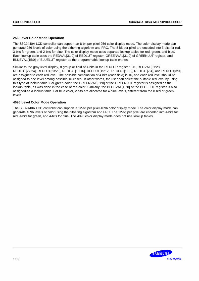
LCD CONTROLLER S3C2440A RISC MICROPROCESSOR
15-6
256 Level Color Mode Operation
The S3C2440A LCD controller can support an 8-bit per pixel 256 color display mode. The color display mode cangenerate 256 levels of color using the dithering algorithm and FRC. The 8-bit per pixel are encoded into 3-bits for red,3-bits for green, and 2-bits for blue. The color display mode uses separate lookup tables for red, green, and blue.Each lookup table uses the REDVAL[31:0] of REDLUT register, GREENVAL[31:0] of GREENLUT register, andBLUEVAL[15:0] of BLUELUT register as the programmable lookup table entries.
Similar to the gray level display, 8 group or field of 4 bits in the REDLUR register, i.e., REDVAL[31:28],REDLUT[27:24], REDLUT[23:20], REDLUT[19:16], REDLUT[15:12], REDLUT[11:8], REDLUT[7:4], and REDLUT[3:0],are assigned to each red level. The possible combination of 4 bits (each field) is 16, and each red level should beassigned to one level among possible 16 cases. In other words, the user can select the suitable red level by usingthis type of lookup table. For green color, the GREENVAL[31:0] of the GREENLUT register is assigned as thelookup table, as was done in the case of red color. Similarly, the BLUEVAL[15:0] of the BLUELUT register is alsoassigned as a lookup table. For blue color, 2 bits are allocated for 4 blue levels, different from the 8 red or greenlevels.
4096 Level Color Mode Operation
The S3C2440A LCD controller can support a 12-bit per pixel 4096 color display mode. The color display mode cangenerate 4096 levels of color using the dithering algorithm and FRC. The 12-bit per pixel are encoded into 4-bits forred, 4-bits for green, and 4-bits for blue. The 4096 color display mode does not use lookup tables.

S3C2440A RISC MICROPROCESSOR LCD CONTROLLER
15-7
DITHERING AND FRAME RATE CONTROL
In case of STN LCD display (except monochrome), video data must be processed by a dithering algorithm. TheDITHFRC block has two functions, such as Time-based Dithering Algorithm for reducing flicker and Frame RateControl (FRC) for displaying gray and color level on the STN panel. The main principle of gray and color level displayon the STN panel based on FRC is described. For example, to display the third gray (3/16) level from a total of 16levels, the 3 times pixel should be on and 13 times pixel off. In other words, 3 frames should be selected among the16 frames, of which 3 frames should have a pixel-on on a specific pixel while the remaining 13 frames should have apixel-off on a specific pixel. These 16 frames should be displayed periodically. This is basic principle on how todisplay the gray level on the screen, so-called gray level display by FRC. The actual example is shown in Table 15-2.To represent the 14th gray level in the table, we should have a 6/7 duty cycle, which mean that there are 6 timespixel-on and one time pixel-off. The other cases for all gray levels are also shown in Table 15-2.
In the STN LCD display, we should be reminded of one item, i.e., Flicker Noise due to the simultaneous pixel-on and-off on adjacent frames. For example, if all pixels on first frame are turned on and all pixels on next frame are turnedoff, the Flicker Noise will be maximized. To reduce the Flicker Noise on the screen, the average probability of pixel-on and -off between frames should be the same. In order to realize this, the Time-based Dithering Algorithm, whichvaries the pattern of adjacent pixels on every frame, should be used. This is explained in detail. For the 16 gray level,FRC should have the following relationship between gray level and FRC. The 15th gray level should always have pixel-on, and the 14th gray level should have 6 times pixel-on and one times pixel-off, and the 13th gray level should have 4times pixel-on and one times pixel-off, ,,,,,,,, , and the 0th gray level should always have pixel-off as shown in Table15-2.
Table 15-2. Dither Duty Cycle Examples
Pre-Dithered Data(gray level number)
Duty Cycle Pre-Dithered Data(gray level number)
Duty Cycle
15 1 7 1/2
14 6/7 6 3/7
13 4/5 5 2/5
12 3/4 4 1/3
11 5/7 3 1/4
10 2/3 2 1/5
9 3/5 1 1/7
8 4/7 0 0

LCD CONTROLLER S3C2440A RISC MICROPROCESSOR
15-8
Display Types
The LCD controller supports 3 types of LCD drivers: 4-bit dual scan, 4-bit single scan, and 8-bit single scan displaymode. Figure 15-2 shows these 3 different display types for monochrome displays, and Figure 15-3 show these 3different display types for color displays.
4-bit Dual Scan Display Type
A 4-bit dual scan display uses 8 parallel data lines to shift data to both the upper and lower halves of the display atthe same time. The 4 bits of data in the 8 parallel data lines are shifted to the upper half and 4 bits of data is shiftedto the lower half, as shown in Figure 15-2. The end of frame is reached when each half of the display has beenshifted and transferred. The 8 pins (VD[7:0]) for the LCD output from the LCD controller can be directly connected tothe LCD driver.
4-bit Single Scan Display Type
A 4-bit single scan display uses 4 parallel data lines to shift data to successive single horizontal lines of the displayat a time, until the entire frame has been shifted and transferred. The 4 pins (VD[3:0]) for the LCD output from theLCD controller can be directly connected to the LCD driver, and the 4 pins (VD[7:4]) for the LCD output are not used.
8-bit Single Scan Display Type
An 8-bit single scan display uses 8 parallel data lines to shift data to successive single horizontal lines of the displayat a time, until the entire frame has been shifted and transferred. The 8 pins (VD[7:0]) for the LCD output from theLCD controller can be directly connected to the LCD driver.
256 Color Displays
Color displays require 3 bits (Red, Green, and Blue) of image data per pixel, so the number of horizontal shiftregisters for each horizontal line corresponds to three times the number of pixels of one horizontal line. These resultsin a horizontal shift register of length 3 times the number of pixels per horizontal line. This RGB is shifted to the LCDdriver as consecutive bits via the parallel data lines. Figure 15-3 shows the RGB and order of the pixels in the paralleldata lines for the 3 types of color displays.
4096 Color Displays
Color displays require 3 bits (Red, Green, and Blue) of image data per pixel, and so the number of horizontal shiftregisters for each horizontal line corresponds to three times the number of pixels of one horizontal line. This RGB isshifted to the LCD driver as consecutive bits via the parallel data lines. This RGB order is determined by thesequence of video data in video buffers.

S3C2440A RISC MICROPROCESSOR LCD CONTROLLER
15-9
MEMORY DATA FORMAT (STN, BSWP = 0)
Mono 4-bit Dual Scan Display:
Video Buffer Memory:
Address Data0000H A[31:0]0004H B[31:0] • • •1000H L[31:0]1004H M[31:0] • • •
Mono 4-bit Single Scan Display & 8-bit SingleScan Display:
Video Buffer Memory:
Address Data0000H A[31:0]0004H B[31:0]0008H C[31:0] • • •
LCD Panel
LCD Panel
A[31] A[30] ...... A[0] B[31] B[30] ...... B[0] ......
L[31] L[30] ...... L[0] M[31] M[30] ...... M[0] ......
A[31] A[30] A[29] ...... A[0] B[31] B[30] ...... B[0] C[31] ...... C[0] ......
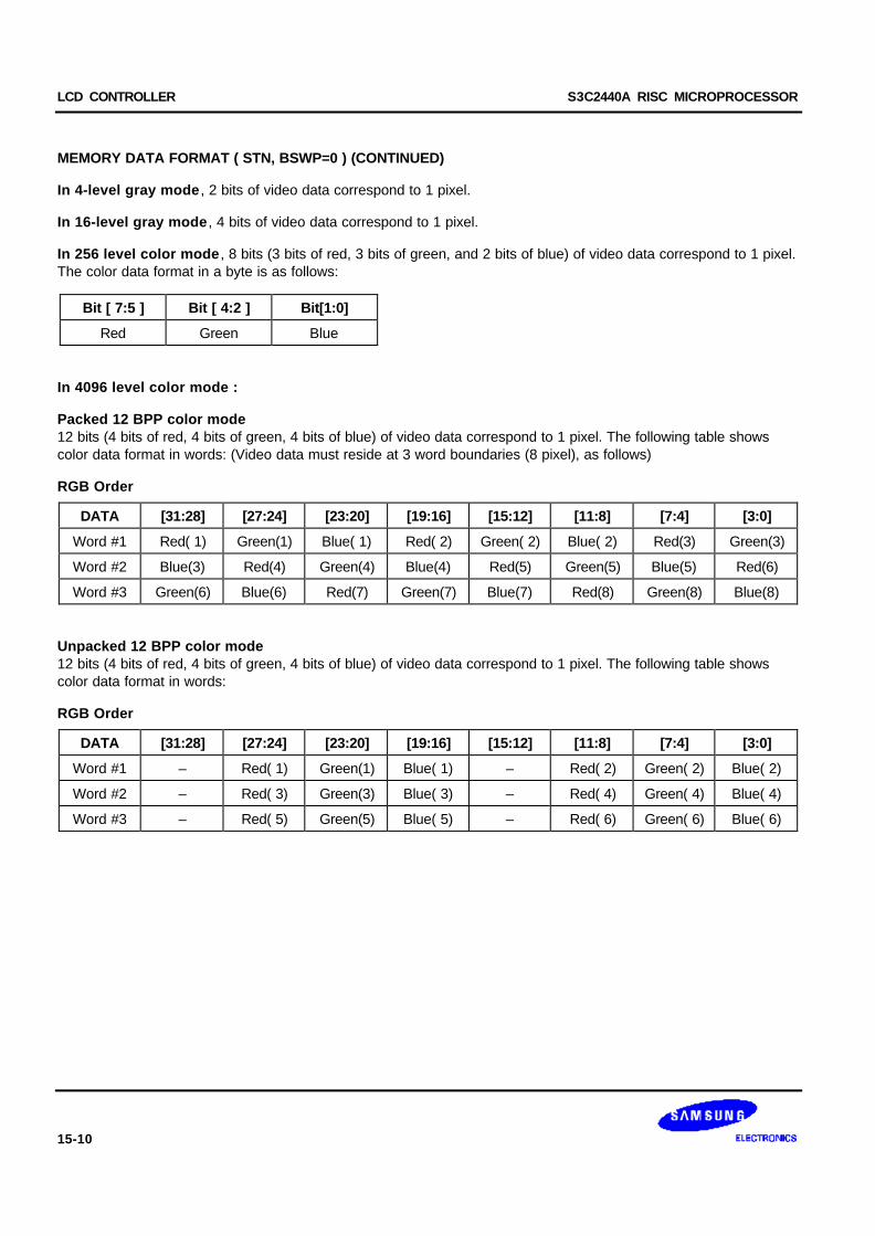
LCD CONTROLLER S3C2440A RISC MICROPROCESSOR
15-10
MEMORY DATA FORMAT ( STN, BSWP=0 ) (CONTINUED)
In 4-level gray mode , 2 bits of video data correspond to 1 pixel.
In 16-level gray mode , 4 bits of video data correspond to 1 pixel.
In 256 level color mode , 8 bits (3 bits of red, 3 bits of green, and 2 bits of blue) of video data correspond to 1 pixel.The color data format in a byte is as follows:
Bit [ 7:5 ] Bit [ 4:2 ] Bit[1:0]
Red Green Blue
In 4096 level color mode :
Packed 12 BPP color mode12 bits (4 bits of red, 4 bits of green, 4 bits of blue) of video data correspond to 1 pixel. The following table showscolor data format in words: (Video data must reside at 3 word boundaries (8 pixel), as follows)
RGB Order
DATA [31:28] [27:24] [23:20] [19:16] [15:12] [11:8] [7:4] [3:0]
Word #1 Red( 1) Green(1) Blue( 1) Red( 2) Green( 2) Blue( 2) Red(3) Green(3)
Word #2 Blue(3) Red(4) Green(4) Blue(4) Red(5) Green(5) Blue(5) Red(6)
Word #3 Green(6) Blue(6) Red(7) Green(7) Blue(7) Red(8) Green(8) Blue(8)
Unpacked 12 BPP color mode12 bits (4 bits of red, 4 bits of green, 4 bits of blue) of video data correspond to 1 pixel. The following table showscolor data format in words:
RGB Order
DATA [31:28] [27:24] [23:20] [19:16] [15:12] [11:8] [7:4] [3:0]
Word #1 – Red( 1) Green(1) Blue( 1) – Red( 2) Green( 2) Blue( 2)
Word #2 – Red( 3) Green(3) Blue( 3) – Red( 4) Green( 4) Blue( 4)
Word #3 – Red( 5) Green(5) Blue( 5) – Red( 6) Green( 6) Blue( 6)
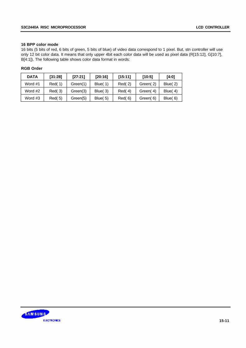
S3C2440A RISC MICROPROCESSOR LCD CONTROLLER
15-11
16 BPP color mode16 bits (5 bits of red, 6 bits of green, 5 bits of blue) of video data correspond to 1 pixel. But, stn controller will useonly 12 bit color data. It means that only upper 4bit each color data will be used as pixel data (R[15:12], G[10:7],B[4:1]). The following table shows color data format in words:
RGB Order
DATA [31:28] [27:21] [20:16] [15:11] [10:5] [4:0]
Word #1 Red( 1) Green(1) Blue( 1) Red( 2) Green( 2) Blue( 2)
Word #2 Red( 3) Green(3) Blue( 3) Red( 4) Green( 4) Blue( 4)
Word #3 Red( 5) Green(5) Blue( 5) Red( 6) Green( 6) Blue( 6)
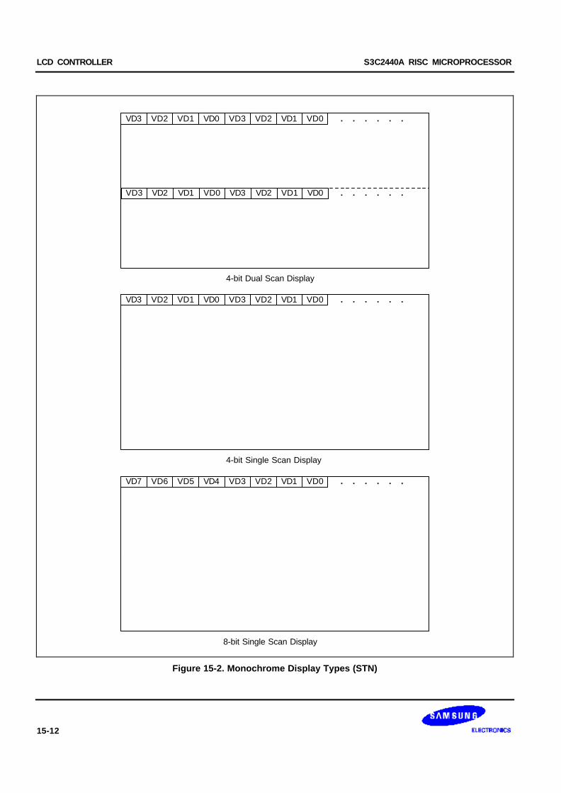
LCD CONTROLLER S3C2440A RISC MICROPROCESSOR
15-12
4-bit Dual Scan Display
4-bit Single Scan Display
8-bit Single Scan Display
. . . . . .
. . . . . .
VD3 VD2 VD1 VD0 VD3 VD2 VD1 VD0
VD3 VD2 VD1 VD0 VD3 VD2 VD1 VD0
VD3 VD2 VD1 VD0 VD3 VD2 VD1 VD0
. . . . . .VD7 VD6 VD5 VD4 VD3 VD2 VD1 VD0
. . . . . .
Figure 15-2. Monochrome Display Types (STN)

S3C2440A RISC MICROPROCESSOR LCD CONTROLLER
15-13
VD3R1
VD2G1
VD1B1
VD0R2
VD3G2
VD2B2
VD1R3
VD0G3
......
1 Pixel
......
4-bit Dual Scan Display
VD3R1
VD2G1
VD1B1
VD0R2
VD3G2
VD2B2
VD1R3
VD0G3
......
1 Pixel
4-bit Single Scan Display
VD7R1
VD6G1
VD5B1
VD4R2
VD7G2
VD6B2
VD5R3
VD4G3
......
1 Pixel
8-bit Single Scan Display
VD7R1
VD6G1
VD5B1
VD4R2
VD3G2
VD2B2
VD1R3
VD0G3
Figure 15-3. Color Display Types (STN)
LCD CONTROLLER S3C2440A RISC MICROPROCESSOR
15-14
Timing Requirements
Image data should be transferred from the memory to the LCD driver using the VD[7:0] signal. VCLK signal is usedto clock the data into the LCD driver's shift register. After each horizontal line of data has been shifted into the LCDdriver's shift register, the VLINE signal is asserted to display the line on the panel.
The VM signal provides an AC signal for the display. The LCD uses the signal to alternate the polarity of the row andcolumn voltages, which are used to turn the pixels on and off, because the LCD plasma tends to deterioratewhenever subjected to a DC voltage. It can be configured to toggle on every frame or to toggle every programmablenumber of VLINE signals.
Figure 15-4 shows the timing requirements for the LCD driver interface.
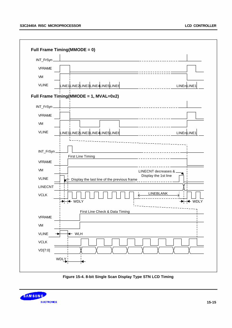
S3C2440A RISC MICROPROCESSOR LCD CONTROLLER
15-15
WDLY
WLH
LINE1LINE2LINE3LINE4LINE5LINE6 LINE1LINEn
First Line Timing
LINECNT decreases &Display the 1st line
LINEBLANK
First Line Check & Data Timing
VFRAME
VM
VLINE
VFRAME
VM
VLINE
LINECNT
VCLK
VFRAME
VM
VLINE
VCLK
VD[7:0]
WDLY WDLY
Display the last line of the previous frame
Full Frame Timing(MMODE = 1, MVAL=0x2)
INT_FrSyn
INT_FrSyn
VFRAME
VM
VLINE
Full Frame Timing(MMODE = 0)
LINE1LINE2LINE3LINE4LINE5LINE6 LINE1LINEn
INT_FrSyn
Figure 15-4. 8-bit Single Scan Display Type STN LCD Timing

LCD CONTROLLER S3C2440A RISC MICROPROCESSOR
15-16
TFT LCD CONTROLLER OPERATION
The TIMEGEN generates the control signals for LCD driver, such as VSYNC, HSYNC, VCLK, VDEN, and LENDsignal. These control signals are highly related with the configurations on the LCDCON1/2/3/4/5 registers in theREGBANK. Base on these programmable configurations on the LCD control registers in the REGBANK, theTIMEGEN can generate the programmable control signals suitable for the support of many different types of LCDdrivers.
The VSYNC signal is asserted to cause the LCD's line pointer to start over at the top of the display.
The VSYNC and HSYNC pulse generation depends on the configurations of both the HOZVAL field and the LINEVALfield in the LCDCON2/3 registers. The HOZVAL and LINEVAL can be determined by the size of the LCD panelaccording to the following equations:
— HOZVAL = (Horizontal display size) -1
— LINEVAL = (Vertical display size) -1
The rate of VCLK signal depends on the CLKVAL field in the LCDCON1 register. Table 15-3 defines the relationshipof VCLK and CLKVAL. The minimum value of CLKVAL is 0.
VCLK(Hz) = HCLK/[(CLKVAL+1)x2]
The frame rate is VSYNC signal frequency. The frame rate is related with the field of VSYNC, VBPD, VFPD,LINEVAL, HSYNC, HBPD, HFPD, HOZVAL, and CLKVAL in LCDCON1 and LCDCON2/3/4 registers. Most LCDdrivers need their own adequate frame rate. The frame rate is calculated as follows:
Frame Rate = 1/ [ (VSPW+1) + (VBPD+1) + (LIINEVAL + 1) + (VFPD+1) x (HSPW+1) + (HBPD +1) + (HFPD+1) + (HOZVAL + 1) x 2 x ( CLKVAL+1 ) / ( HCLK ) ]
Table 15-3. Relation between VCLK and CLKVAL (TFT, HCLK = 60MHz)
CLKVAL 60MHz/X VCLK
1 60 MHz/4 15.0 MHz
2 60 MHz/6 10.0 MHz
: : :
1023 60 MHz/2048 30.0 kHz
VIDEO OPERATION
The TFT LCD controller within the S3C2440A supports 1, 2, 4 or 8 bpp (bit per pixel) palettized color displays and 16or 24 bpp non-palettized true-color displays.
256 Color Palette
The S3C2440A can support the 256 color palette for various selection of color mapping, providing flexible operationfor users.

S3C2440A RISC MICROPROCESSOR LCD CONTROLLER
15-17
MEMORY DATA FORMAT (TFT)
This section includes some examples of each display mode.
24BPP Display
(BSWP = 0, HWSWP = 0, BPP24BL = 0)
D[31:24] D[23:0]
000H Dummy Bit P1
004H Dummy Bit P2
008H Dummy Bit P3
...
(BSWP = 0, HWSWP = 0, BPP24BL = 1)
D[31:8] D[7:0]
000H P1 Dummy Bit
004H P2 Dummy Bit
008H P3 Dummy Bit
...
P1 P2 P3 P4 P5 ......
LCD Panel
VD Pin Descriptions at 24BPP
VD 23 22 21 20 19 18 17 16 15 14 13 12 11 10 9 8 7 6 5 4 3 2 1 0
RED 7 6 5 4 3 2 1 0
GREEN 7 6 5 4 3 2 1 0
BLUE 7 6 5 4 3 2 1 0

LCD CONTROLLER S3C2440A RISC MICROPROCESSOR
15-18
16BPP Display
(BSWP = 0, HWSWP = 0)
D[31:16] D[15:0]
000H P1 P2
004H P3 P4
008H P5 P6
...
(BSWP = 0, HWSWP = 1)
D[31:16] D[15:0]
000H P2 P1
004H P4 P3
008H P6 P5
...
P1 P2 P3 P4 P5 ......
LCD Panel
VD Pin Descriptions at 16BPP
(5:6:5)
VD 23 22 21 20 19 18 17 16 15 14 13 12 11 10 9 8 7 6 5 4 3 2 1 0
RED 4 3 2 1 0 NC NC NC
GREEN 5 4 3 2 1 0
BLUE 4 3 2 1 0
(5:5:5:I)
VD 23 22 21 20 19 18 17 16 15 14 13 12 11 10 9 8 7 6 5 4 3 2 1 0
RED 4 3 2 1 0 I NC NC NC
GREEN 4 3 2 1 0 I
BLUE 4 3 2 1 0 I
NOTE: The unused VD pins can be used as GPIO
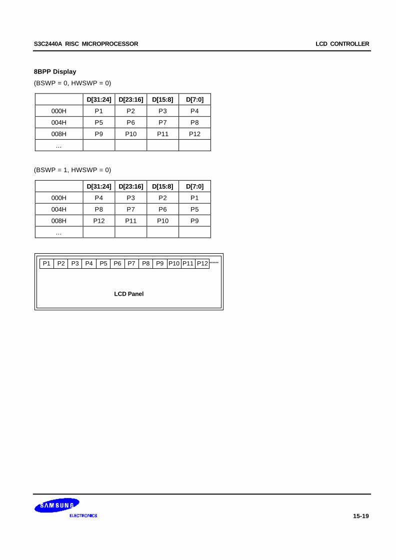
S3C2440A RISC MICROPROCESSOR LCD CONTROLLER
15-19
8BPP Display
(BSWP = 0, HWSWP = 0)
D[31:24] D[23:16] D[15:8] D[7:0]
000H P1 P2 P3 P4
004H P5 P6 P7 P8
008H P9 P10 P11 P12
...
(BSWP = 1, HWSWP = 0)
D[31:24] D[23:16] D[15:8] D[7:0]
000H P4 P3 P2 P1
004H P8 P7 P6 P5
008H P12 P11 P10 P9
...
P1 P2 P3 P4 P5 ......
LCD Panel
P6 P7 P8 P10 P11 P12P9
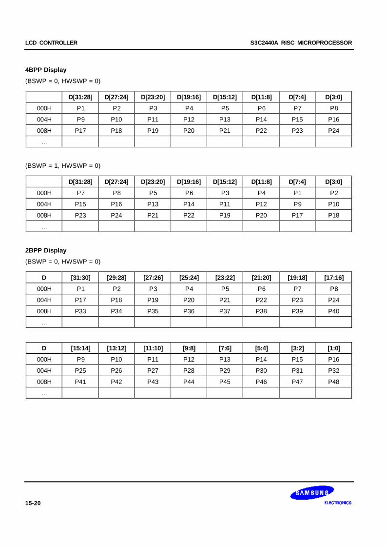
LCD CONTROLLER S3C2440A RISC MICROPROCESSOR
15-20
4BPP Display
(BSWP = 0, HWSWP = 0)
D[31:28] D[27:24] D[23:20] D[19:16] D[15:12] D[11:8] D[7:4] D[3:0]
000H P1 P2 P3 P4 P5 P6 P7 P8
004H P9 P10 P11 P12 P13 P14 P15 P16
008H P17 P18 P19 P20 P21 P22 P23 P24
...
(BSWP = 1, HWSWP = 0)
D[31:28] D[27:24] D[23:20] D[19:16] D[15:12] D[11:8] D[7:4] D[3:0]
000H P7 P8 P5 P6 P3 P4 P1 P2
004H P15 P16 P13 P14 P11 P12 P9 P10
008H P23 P24 P21 P22 P19 P20 P17 P18
...
2BPP Display
(BSWP = 0, HWSWP = 0)
D [31:30] [29:28] [27:26] [25:24] [23:22] [21:20] [19:18] [17:16]
000H P1 P2 P3 P4 P5 P6 P7 P8
004H P17 P18 P19 P20 P21 P22 P23 P24
008H P33 P34 P35 P36 P37 P38 P39 P40
...
D [15:14] [13:12] [11:10] [9:8] [7:6] [5:4] [3:2] [1:0]
000H P9 P10 P11 P12 P13 P14 P15 P16
004H P25 P26 P27 P28 P29 P30 P31 P32
008H P41 P42 P43 P44 P45 P46 P47 P48
...
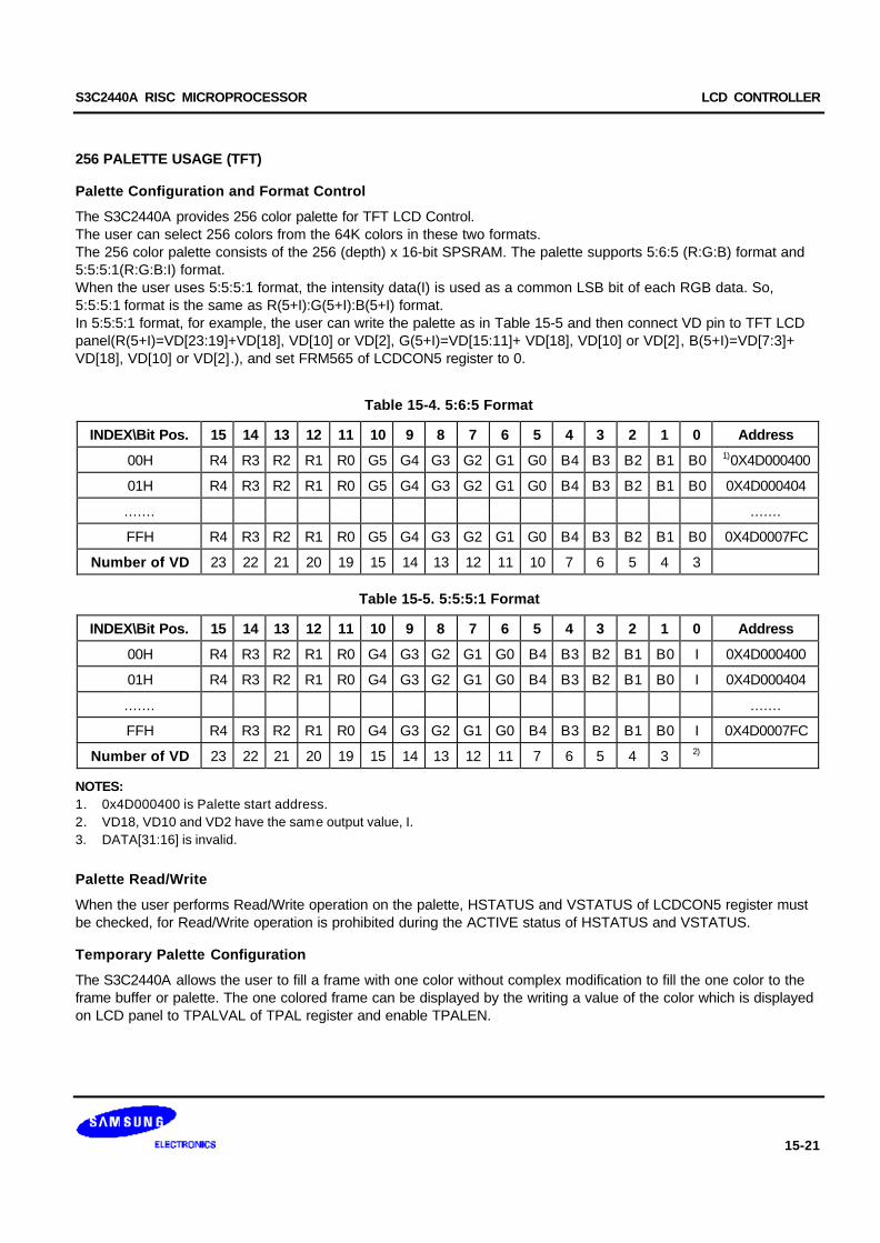
S3C2440A RISC MICROPROCESSOR LCD CONTROLLER
15-21
256 PALETTE USAGE (TFT)
Palette Configuration and Format Control
The S3C2440A provides 256 color palette for TFT LCD Control.The user can select 256 colors from the 64K colors in these two formats.The 256 color palette consists of the 256 (depth) x 16-bit SPSRAM. The palette supports 5:6:5 (R:G:B) format and5:5:5:1(R:G:B:I) format.When the user uses 5:5:5:1 format, the intensity data(I) is used as a common LSB bit of each RGB data. So,5:5:5:1 format is the same as R(5+I):G(5+I):B(5+I) format.In 5:5:5:1 format, for example, the user can write the palette as in Table 15-5 and then connect VD pin to TFT LCDpanel(R(5+I)=VD[23:19]+VD[18], VD[10] or VD[2], G(5+I)=VD[15:11]+ VD[18], VD[10] or VD[2], B(5+I)=VD[7:3]+VD[18], VD[10] or VD[2].), and set FRM565 of LCDCON5 register to 0.
Table 15-4. 5:6:5 Format
INDEX\Bit Pos. 15 14 13 12 11 10 9 8 7 6 5 4 3 2 1 0 Address
00H R4 R3 R2 R1 R0 G5 G4 G3 G2 G1 G0 B4 B3 B2 B1 B0 1)0X4D000400
01H R4 R3 R2 R1 R0 G5 G4 G3 G2 G1 G0 B4 B3 B2 B1 B0 0X4D000404
....... .......
FFH R4 R3 R2 R1 R0 G5 G4 G3 G2 G1 G0 B4 B3 B2 B1 B0 0X4D0007FC
Number of VD 23 22 21 20 19 15 14 13 12 11 10 7 6 5 4 3
Table 15-5. 5:5:5:1 Format
INDEX\Bit Pos. 15 14 13 12 11 10 9 8 7 6 5 4 3 2 1 0 Address
00H R4 R3 R2 R1 R0 G4 G3 G2 G1 G0 B4 B3 B2 B1 B0 I 0X4D000400
01H R4 R3 R2 R1 R0 G4 G3 G2 G1 G0 B4 B3 B2 B1 B0 I 0X4D000404
....... .......
FFH R4 R3 R2 R1 R0 G4 G3 G2 G1 G0 B4 B3 B2 B1 B0 I 0X4D0007FC
Number of VD 23 22 21 20 19 15 14 13 12 11 7 6 5 4 3 2)
NOTES:1. 0x4D000400 is Palette start address.2. VD18, VD10 and VD2 have the same output value, I.3. DATA[31:16] is invalid.
Palette Read/Write
When the user performs Read/Write operation on the palette, HSTATUS and VSTATUS of LCDCON5 register mustbe checked, for Read/Write operation is prohibited during the ACTIVE status of HSTATUS and VSTATUS.
Temporary Palette Configuration
The S3C2440A allows the user to fill a frame with one color without complex modification to fill the one color to theframe buffer or palette. The one colored frame can be displayed by the writing a value of the color which is displayedon LCD panel to TPALVAL of TPAL register and enable TPALEN.

LCD CONTROLLER S3C2440A RISC MICROPROCESSOR
15-22
1 2 3 4 5
LCD Panel
16BPP 5:5:5+1 Format(Non-Palette)
A[31] A[30] A[29] A[28] A[27] A[26]A[25] A[24] A[23] A[22] A[21] A[20] A[19]A[18] A[17] A[16]
R4 R3 R2 R1 R0 G4 G3 G2 G1 G0 R4 B3 B2 B1 B0 I
A[15] A[14] A[13] A[12] A[11] A[10] A[9] A[8] A[7] A[6] A[5] A[4] A[3] A[2] A[1] A[0]
R4 R3 R2 R1 R0 G4 G3 G2 G1 G0 R4 B3 B2 B1 B0 I
1 2 3 4 5
LCD Panel
16BPP 5:6:5 Format(Non-Palette)
A[31] A[30] A[29] A[28] A[27] A[26]A[25] A[24] A[23] A[22] A[21] A[20] A[19]A[18] A[17] A[16]
A[15] A[14] A[13] A[12]A[11] A[10] A[9] A[8] A[7] A[6] A[5] A[4] A[3] A[2] A[1] A[0]
R4 R3 R2 R1 R0 G5 G4 G3 G2 G1 G0 B4 B3 B2 B1 B0
R4 R3 R2 R1 R0 G5 G4 G3 G2 G1 G0 B4 B3 B2 B1 B0
Figure 15-5. 16BPP Display Types (TFT)

S3C2440A RISC MICROPROCESSOR LCD CONTROLLER
15-23
INT_FrSyn
VSYNC
HSYNC
VDEN
HSYNC
VCLK
VD
LEND
VBPD+1VSPW+1
VFPD+1
HBPD+1 HFPD+1HSPW+1
VDEN
1 Frame
1 Line
LINEVAL +1
HOZVAL+1
Figure 15-6. TFT LCD Timing Example
LCD CONTROLLER S3C2440A RISC MICROPROCESSOR
15-24
SAMSUNG TFT LCD PANEL (3.5” PORTRAIT / 256K COLOR / REFLECTIVE A-SI/TRANSFLECTIVE A-SI TFTLCD)
The S3C2440A supports following SEC TFT LCD panels.
1. SAMSUNG 3.5” Portrait / 256K Color /Reflective a-Si TFT LCD. LTS350Q1-PD1: TFT LCD panel with touch panel and front light unit LTS350Q1-PD2: TFT LCD panel only
2. SAMSUNG 3.5” Portrait / 256K Color /Transflective a-Si TFT LCD. LTS350Q1-PE1: TFT LCD panel with touch panel and front light unit LTS350Q1-PE2: TFT LCD panel only
The S3C2440A provides timing signals as follows to use LTS350Q1-PD1 / PD2 and LTS350Q1-PE1 / PE2
LTS350Q1-PD1 / PD2 LTS350Q1-PE1 / PE2
STH: Horizontal Start PulseTP: Source Driver Data Load Pulse
INV: Digital Data InversionLCD_HCLK: Horizontal Sampling Clock
CPV: Vertical Shift ClockSTV: Vertical Start Pulse
OE: Gate On EnableREV: Inversion Signal
REVB: Inversion Signal
STH: Horizontal Start PulseTP: Source Driver Data Load Pulse
INV: Digital Data InversionLCD_HCLK: Horizontal Sampling Clock
CPV: Vertical Shift ClockSTV: Vertical Start Pulse
LCCINV: Source drive IC sampling inversion signalREV: VCOM modulation Signal
REVB: Inversion Signal
So, LTS350Q1-PD1/2 and PE1/2 can be connected with the S3C2440A without using the additional timing controllogic. But the user should additionally apply Vcom generator circuit, various voltages, INV signal and Gray scalevoltage generator circuit, which is recommended by PRODUCT INFORMATION (SPEC) of LTS350Q1-PD1/2 andPE1/2. Detailed timing diagram is also described in PRODUCT INFORMATION (SPEC) of LTS350Q1-PD1/2 andPE1/2.
Refer to the documentation (PRODUCT INFORMATION of LTS350Q1-PD1/2 and PE1/2), which is prepared byAMLCD Technical Customer Center of Samsung Electronics Co., LTD.
Caution:— The S3C2440A has HCLK, working as the clock of AHB bus.— SEC TFT LCD panel (LTS350Q1-PD1/2 and PE1/2) has Horizontal Sampling Clock (HCLK).— These two HCLKs may cause a confusion. So, note that HCLK of the S3C2440A is HCLK and other HCLK
of the LTS350 is LCD_HCLK.
Check that the HCLK of SEC TFT LCD panel (LTS350Q1-PD1/2 and PE1/2) is changed to LCD_HCLK.

S3C2440A RISC MICROPROCESSOR LCD CONTROLLER
15-25
VIRTUAL DISPLAY (TFT/STN)
The S3C2440A supports hardware horizontal or vertical scrolling. If the screen is scrolled, the fields of LCDBASEUand LCDBASEL in LCDSADDR1/2 registers need to be changed (see Figure 15-8), except the values ofPAGEWIDTH and OFFSIZE.The video buffer in which the image is stored should be larger than the LCD panel screen in size.
This is the data of line 1 of virtual screen. This is the data of line 1 of virtual screen.
This is the data of line 2 of virtual screen. This is the data of line 2 of virtual screen.
This is the data of line 3 of virtual screen. This is the data of line 3 of virtual screen.
This is the data of line 4 of virtual screen. This is the data of line 4 of virtual screen.
This is the data of line 5 of virtual screen. This is the data of line 5 of virtual screen.
This is the data of line 6 of virtual screen. This is the data of line 6 of virtual screen.
This is the data of line 7 of virtual screen. This is the data of line 7 of virtual screen.
This is the data of line 8 of virtual screen. This is the data of line 8 of virtual screen.
This is the data of line 9 of virtual screen. This is the data of line 9 of virtual screen.
This is the data of line 10 of virtual screen. This is the data of line 10 of virtual screen.
This is the data of line 11 of virtual screen. This is the data of line 11 of virtual screen.
.
.
.Before Scrolling
View Port(The same sizeof LCD panel.)
LINEVAL + 1
OFFSIZEPAGEWIDTH
This is the data of line 1 of virtual screen. This is the data of line 1 of virtual screen.
This is the data of line 2 of virtual screen. This is the data of line 2 of virtual screen.
This is the data of line 3 of virtual screen. This is the data of line 3 of virtual screen.
This is the data of line 4 of virtual screen. This is the data of line 4 of virtual screen.
This is the data of line 5 of virtual screen. This is the data of line 5 of virtual screen.
This is the data of line 6 of virtual screen. This is the data of line 6 of virtual screen.
This is the data of line 7 of virtual screen. This is the data of line 7 of virtual screen.
This is the data of line 8 of virtual screen. This is the data of line 8 of virtual screen.
This is the data of line 9 of virtual screen. This is the data of line 9 of virtual screen.
This is the data of line 10 of virtual screen. This is the data of line 10 of virtual screen.
This is the data of line 11 of virtual screen. This is the data of line 11 of virtual screen.
.
.
.
After Scrolling
LCDBASEU
LCDBASEL
OFFSIZE
Figure 15-7. Example of Scrolling in Virtual Display (Single Scan)

LCD CONTROLLER S3C2440A RISC MICROPROCESSOR
15-26
LCD POWER ENABLE (STN/TFT)
The S3C2440A provides Power enable (PWREN) function. When PWREN is set to make PWREN signal enabled,the output value of LCD_PWREN pin is controlled by ENVID. In other words, If LCD_PWREN pin is connected to thepower on/off control pin of the LCD panel, the power of LCD panel is controlled by the setting of ENVID automatically.
The S3C2440A also supports INVPWREN bit to invert polarity of the PWREN signal.
This function is available only when LCD panel has its own power on/off control port and when port is connected toLCD_PWREN pin.
VSYNC
HSYNC
VDEN
LCD_PWREN
1 FRAME
ENVID
LCD Panel On
TFT LCD
VLINE
VFRAME
STN LCD
LCD_PWREN LCD Panel On
ENVID
Figure 15-8. Example of PWREN Function (PWREN=1, INVPWREN=0)
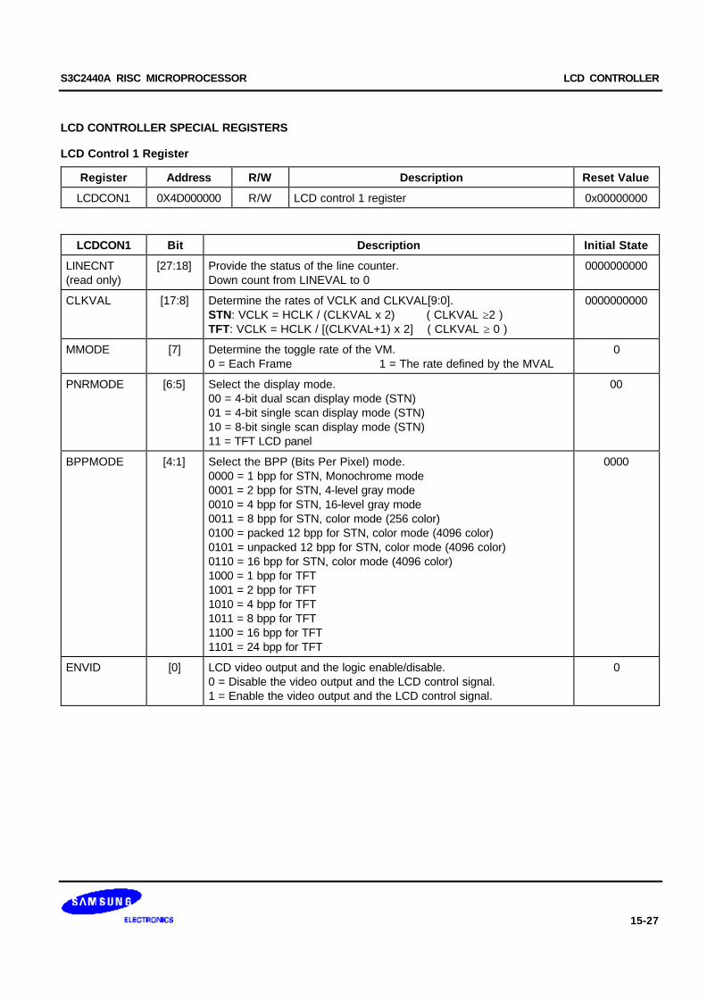
S3C2440A RISC MICROPROCESSOR LCD CONTROLLER
15-27
LCD CONTROLLER SPECIAL REGISTERS
LCD Control 1 Register
Register Address R/W Description Reset Value
LCDCON1 0X4D000000 R/W LCD control 1 register 0x00000000
LCDCON1 Bit Description Initial State
LINECNT(read only)
[27:18] Provide the status of the line counter.Down count from LINEVAL to 0
0000000000
CLKVAL [17:8] Determine the rates of VCLK and CLKVAL[9:0].STN: VCLK = HCLK / (CLKVAL x 2) ( CLKVAL ≥2 )TFT: VCLK = HCLK / [(CLKVAL+1) x 2] ( CLKVAL ≥ 0 )
0000000000
MMODE [7] Determine the toggle rate of the VM.0 = Each Frame 1 = The rate defined by the MVAL
0
PNRMODE [6:5] Select the display mode.00 = 4-bit dual scan display mode (STN)01 = 4-bit single scan display mode (STN)10 = 8-bit single scan display mode (STN)11 = TFT LCD panel
00
BPPMODE [4:1] Select the BPP (Bits Per Pixel) mode.0000 = 1 bpp for STN, Monochrome mode0001 = 2 bpp for STN, 4-level gray mode0010 = 4 bpp for STN, 16-level gray mode0011 = 8 bpp for STN, color mode (256 color)0100 = packed 12 bpp for STN, color mode (4096 color)0101 = unpacked 12 bpp for STN, color mode (4096 color)0110 = 16 bpp for STN, color mode (4096 color)1000 = 1 bpp for TFT1001 = 2 bpp for TFT1010 = 4 bpp for TFT1011 = 8 bpp for TFT1100 = 16 bpp for TFT1101 = 24 bpp for TFT
0000
ENVID [0] LCD video output and the logic enable/disable.0 = Disable the video output and the LCD control signal.1 = Enable the video output and the LCD control signal.
0
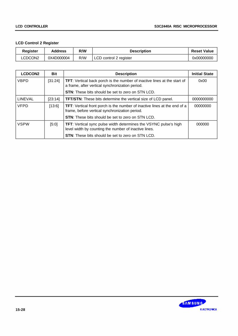
LCD CONTROLLER S3C2440A RISC MICROPROCESSOR
15-28
LCD Control 2 Register
Register Address R/W Description Reset Value
LCDCON2 0X4D000004 R/W LCD control 2 register 0x00000000
LCDCON2 Bit Description Initial State
VBPD [31:24] TFT: Vertical back porch is the number of inactive lines at the start ofa frame, after vertical synchronization period.
STN: These bits should be set to zero on STN LCD.
0x00
LINEVAL [23:14] TFT/STN: These bits determine the vertical size of LCD panel. 0000000000
VFPD [13:6] TFT: Vertical front porch is the number of inactive lines at the end of aframe, before vertical synchronization period.
STN: These bits should be set to zero on STN LCD.
00000000
VSPW [5:0] TFT: Vertical sync pulse width determines the VSYNC pulse's highlevel width by counting the number of inactive lines.
STN: These bits should be set to zero on STN LCD.
000000
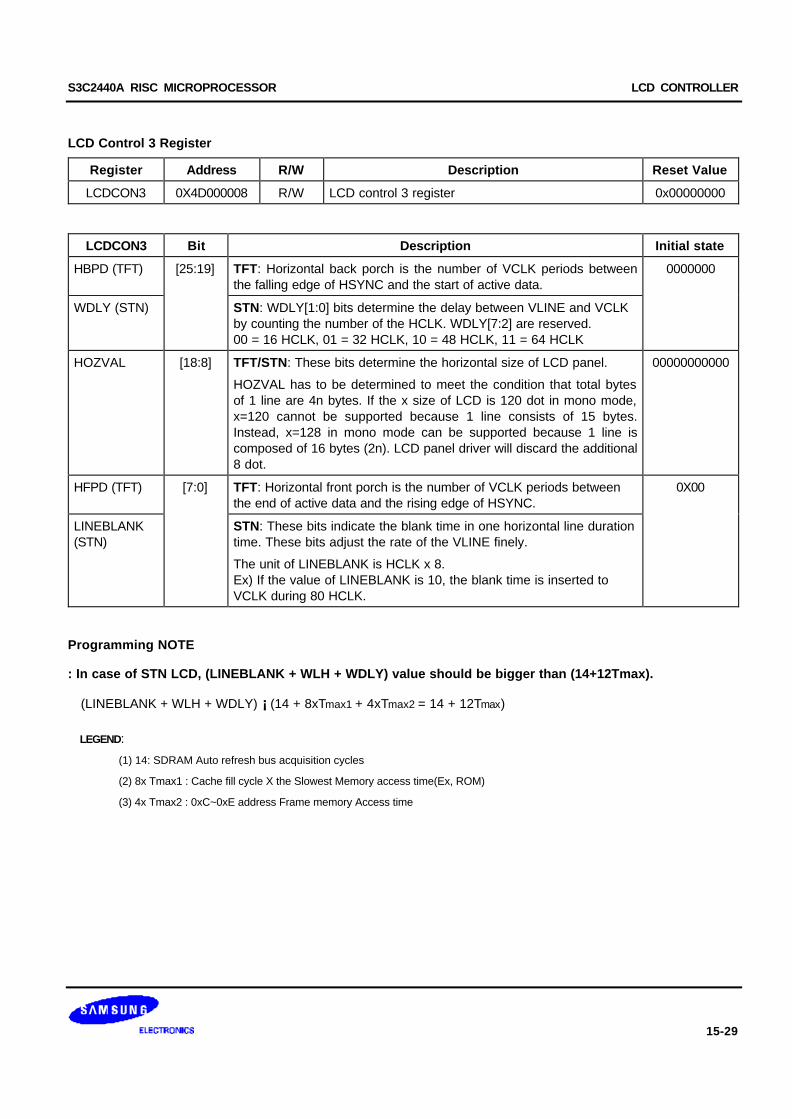
S3C2440A RISC MICROPROCESSOR LCD CONTROLLER
15-29
LCD Control 3 Register
Register Address R/W Description Reset Value
LCDCON3 0X4D000008 R/W LCD control 3 register 0x00000000
LCDCON3 Bit Description Initial state
HBPD (TFT) [25:19] TFT: Horizontal back porch is the number of VCLK periods betweenthe falling edge of HSYNC and the start of active data.
0000000
WDLY (STN) STN: WDLY[1:0] bits determine the delay between VLINE and VCLKby counting the number of the HCLK. WDLY[7:2] are reserved.00 = 16 HCLK, 01 = 32 HCLK, 10 = 48 HCLK, 11 = 64 HCLK
HOZVAL [18:8] TFT/STN: These bits determine the horizontal size of LCD panel.
HOZVAL has to be determined to meet the condition that total bytesof 1 line are 4n bytes. If the x size of LCD is 120 dot in mono mode,x=120 cannot be supported because 1 line consists of 15 bytes.Instead, x=128 in mono mode can be supported because 1 line iscomposed of 16 bytes (2n). LCD panel driver will discard the additional8 dot.
00000000000
HFPD (TFT) [7:0] TFT: Horizontal front porch is the number of VCLK periods betweenthe end of active data and the rising edge of HSYNC.
0X00
LINEBLANK(STN)
STN: These bits indicate the blank time in one horizontal line durationtime. These bits adjust the rate of the VLINE finely.
The unit of LINEBLANK is HCLK x 8.Ex) If the value of LINEBLANK is 10, the blank time is inserted toVCLK during 80 HCLK.
Programming NOTE
: In case of STN LCD, (LINEBLANK + WLH + WDLY) value should be bigger than (14+12Tmax).
(LINEBLANK + WLH + WDLY) ¡ (14 + 8xTmax1 + 4xTmax2 = 14 + 12Tmax)
LEGEND:
(1) 14: SDRAM Auto refresh bus acquisition cycles
(2) 8x Tmax1 : Cache fill cycle X the Slowest Memory access time(Ex, ROM)
(3) 4x Tmax2 : 0xC~0xE address Frame memory Access time

LCD CONTROLLER S3C2440A RISC MICROPROCESSOR
15-30
LCD Control 4 Register
Register Address R/W Description Reset Value
LCDCON4 0X4D00000C R/W LCD control 4 register 0x00000000
LCDCON4 Bit Description Initial state
MVAL [15:8] STN: These bit define the rate at which the VM signal will toggle if theMMODE bit is set to logic '1'.
0X00
HSPW(TFT) [7:0] TFT: Horizontal sync pulse width determines the HSYNC pulse's highlevel width by counting the number of the VCLK.
0X00
WLH(STN) STN: WLH[1:0] bits determine the VLINE pulse's high level width bycounting the number of the HCLK.WLH[7:2] are reserved.
00 = 16 HCLK, 01 = 32 HCLK, 10 = 48 HCLK, 11 = 64 HCLK
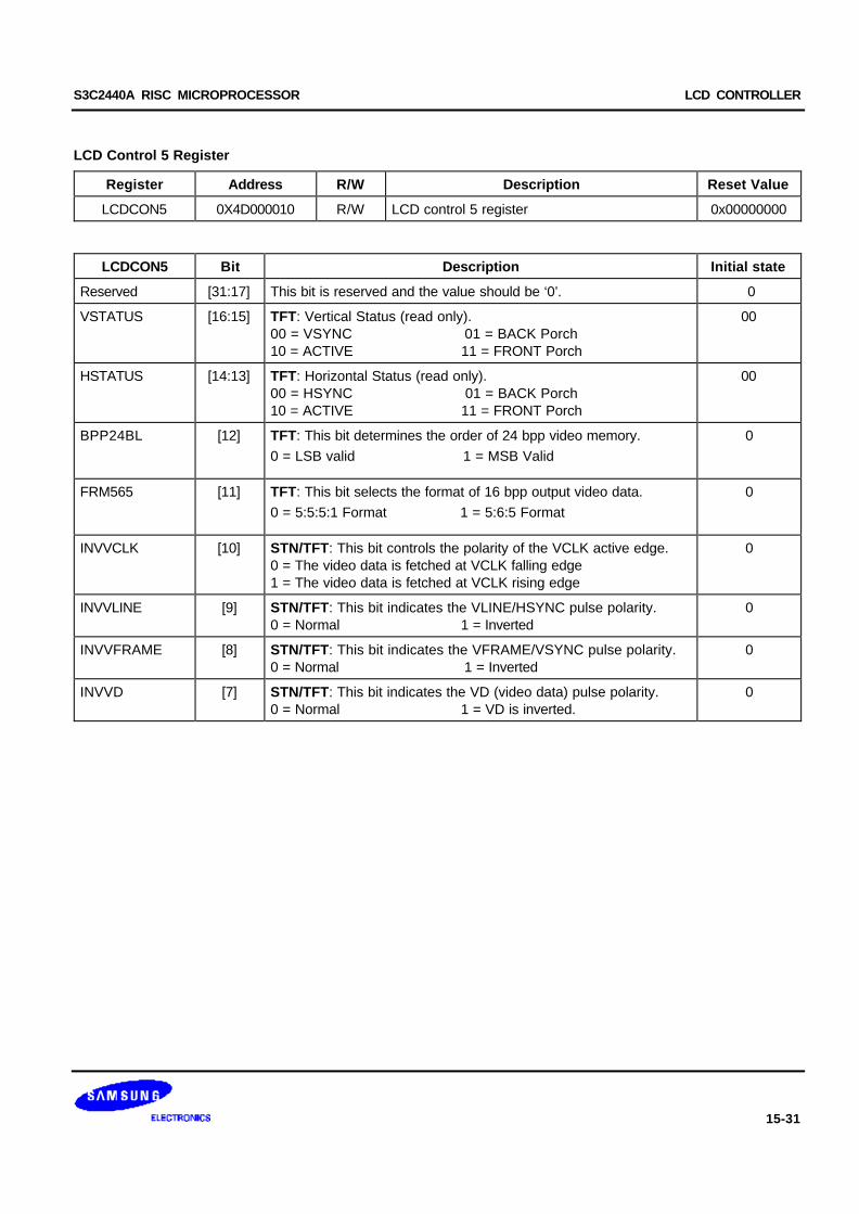
S3C2440A RISC MICROPROCESSOR LCD CONTROLLER
15-31
LCD Control 5 Register
Register Address R/W Description Reset Value
LCDCON5 0X4D000010 R/W LCD control 5 register 0x00000000
LCDCON5 Bit Description Initial state
Reserved [31:17] This bit is reserved and the value should be ‘0’. 0
VSTATUS [16:15] TFT: Vertical Status (read only).00 = VSYNC 01 = BACK Porch10 = ACTIVE 11 = FRONT Porch
00
HSTATUS [14:13] TFT: Horizontal Status (read only).00 = HSYNC 01 = BACK Porch10 = ACTIVE 11 = FRONT Porch
00
BPP24BL [12] TFT: This bit determines the order of 24 bpp video memory.0 = LSB valid 1 = MSB Valid
0
FRM565 [11] TFT: This bit selects the format of 16 bpp output video data.0 = 5:5:5:1 Format 1 = 5:6:5 Format
0
INVVCLK [10] STN/TFT: This bit controls the polarity of the VCLK active edge.0 = The video data is fetched at VCLK falling edge1 = The video data is fetched at VCLK rising edge
0
INVVLINE [9] STN/TFT: This bit indicates the VLINE/HSYNC pulse polarity.0 = Normal 1 = Inverted
0
INVVFRAME [8] STN/TFT: This bit indicates the VFRAME/VSYNC pulse polarity.0 = Normal 1 = Inverted
0
INVVD [7] STN/TFT: This bit indicates the VD (video data) pulse polarity.0 = Normal 1 = VD is inverted.
0

LCD CONTROLLER S3C2440A RISC MICROPROCESSOR
15-32
LCD Control 5 Register (Continued)
LCDCON5 Bit Description Initial state
INVVDEN [6] TFT: This bit indicates the VDEN signal polarity.0 = normal 1 = inverted
0
INVPWREN [5] STN/TFT: This bit indicates the PWREN signal polarity.0 = normal 1 = inverted
0
INVLEND [4] TFT: This bit indicates the LEND signal polarity.0 = normal 1 = inverted
0
PWREN [3] STN/TFT: LCD_PWREN output signal enable/disable.0 = Disable PWREN signal 1 = Enable PWREN signal
0
ENLEND [2] TFT: LEND output signal enable/disable.0 = Disable LEND signal 1 = Enable LEND signal
0
BSWP [1] STN/TFT: Byte swap control bit.0 = Swap Disable 1 = Swap Enable
0
HWSWP [0] STN/TFT: Half-Word swap control bit.0 = Swap Disable 1 = Swap Enable
0

S3C2440A RISC MICROPROCESSOR LCD CONTROLLER
15-33
FRAME BUFFER START ADDRESS 1 REGISTER
Register Address R/W Description Reset Value
LCDSADDR1 0X4D000014 R/W STN/TFT: Frame buffer start address 1 register 0x00000000
LCDSADDR1 Bit Description Initial State
LCDBANK [29:21] These bits indicate A[30:22] of the bank location for the video buffer inthe system memory. LCDBANK value cannot be changed even whenmoving the view port. LCD frame buffer should be within aligned 4MBregion, which ensures that LCDBANK value will not be changed whenmoving the view port. So, care should be taken to use the malloc()function.
0x00
LCDBASEU [20:0] For dual-scan LCD : These bits indicate A[21:1] of the start address ofthe upper address counter, which is for the upper frame memory ofdual scan LCD or the frame memory of single scan LCD.
For single-scan LCD : These bits indicate A[21:1] of the start addressof the LCD frame buffer.
0x000000
FRAME Buffer Start Address 2 Register
Register Address R/W Description Reset Value
LCDSADDR2 0X4D000018 R/W STN/TFT: Frame buffer start address 2 register 0x00000000
LCDSADDR2 Bit Description Initial State
LCDBASEL [20:0] For dual-scan LCD: These bits indicate A[21:1] of the start address ofthe lower address counter, which is used for the lower frame memoryof dual scan LCD.
For single scan LCD: These bits indicate A[21:1] of the end addressof the LCD frame buffer.
LCDBASEL = ((the frame end address) >>1) + 1 = LCDBASEU +
(PAGEWIDTH+OFFSIZE) x (LINEVAL+1)
0x0000
NOTE: Users can change the LCDBASEU and LCDBASEL values for scrolling while the LCD controller is turned on.But, users must not change the value of the LCDBASEU and LCDBASEL registers at the end of FRAME by referring to the LINECNT field in LCDCON1 register, for the LCD FIFO fetches the next frame data prior to the change in theframe.So, if you change the frame, the pre-fetched FIFO data will be obsolete and LCD controller will display an incorrect screen. To check the LINECNT, interrupts should be masked. If any interrupt is executed just after reading
LINECNT, the read LINECNT value may be obsolete because of the execution time of Interrupt ServiceRoutine (ISR).
LCD CONTROLLER S3C2440A RISC MICROPROCESSOR
15-34
FRAME Buffer Start Address 3 Register
Register Address R/W Description Reset Value
LCDSADDR3 0X4D00001C R/W STN/TFT: Virtual screen address set 0x00000000
LCDSADDR3 Bit Description Initial State
OFFSIZE [21:11] Virtual screen offset size (the number of half words).This value defines the difference between the address of the last halfword displayed on the previous LCD line and the address of the firsthalf word to be displayed in the new LCD line.
00000000000
PAGEWIDTH [10:0] Virtual screen page width (the number of half words).This value defines the width of the view port in the frame.
000000000
NOTE: The values of PAGEWIDTH and OFFSIZE must be changed when ENVID bit is 0.
Example 1. LCD panel = 320 x 240, 16gray, single scan Frame start address = 0x0c500000 Offset dot number = 2048 dots ( 512 half words )
LINEVAL = 240-1 = 0xef PAGEWIDTH = 320 x 4 / 16 = 0x50 OFFSIZE = 512 = 0x200 LCDBANK = 0x0c500000 >> 22 = 0x31 LCDBASEU = 0x100000 >> 1 = 0x80000 LCDBASEL = 0x80000 + ( 0x50 + 0x200 ) x ( 0xef + 1 ) = 0xa2b00
Example 2. LCD panel = 320 x 240, 16gray, dual scan Frame start address = 0x0c500000 Offset dot number = 2048 dots ( 512 half words )
LINEVAL = 120-1 = 0x77 PAGEWIDTH = 320 x 4 / 16 = 0x50 OFFSIZE = 512 = 0x200 LCDBANK = 0x0c500000 >> 22 = 0x31 LCDBASEU = 0x100000 >> 1 = 0x80000 LCDBASEL = 0x80000 + ( 0x50 + 0x200 ) x ( 0x77 + 1 ) = 0x91580
Example 3. LCD panel = 320*240, color, single scan Frame start address = 0x0c500000 Offset dot number = 1024 dots ( 512 half words )
LINEVAL = 240-1 = 0xef PAGEWIDTH = 320 x 8 / 16 = 0xa0 OFFSIZE = 512 = 0x200 LCDBANK = 0x0c500000 >> 22 = 0x31 LCDBASEU = 0x100000 >> 1 = 0x80000 LCDBASEL = 0x80000 + ( 0xa0 + 0x200 ) x ( 0xef + 1 ) = 0xa7600
S3C2440A RISC MICROPROCESSOR LCD CONTROLLER
15-35
RED Lookup Table Register
Register Address R/W Description Reset Value
REDLUT 0X4D000020 R/W STN: Red lookup table register 0x00000000
REDLUT Bit Description Initial State
REDVAL [31:0] These bits define which of the 16 shades will be chosen by each ofthe 8 possible red combinations.
000 = REDVAL[3:0], 001 = REDVAL[7:4]010 = REDVAL[11:8], 011 = REDVAL[15:12]100 = REDVAL[19:16], 101 = REDVAL[23:20]110 = REDVAL[27:24], 111 = REDVAL[31:28]
0x00000000
GREEN Lookup Table Register
Register Address R/W Description Reset Value
GREENLUT 0X4D000024 R/W STN: Green lookup table register 0x00000000
GREENLUT Bit Description Initial State
GREENVAL [31:0] These bits define which of the 16 shades will be chosen by each ofthe 8 possible green combinations.
000 = GREENVAL[3:0], 001 = GREENVAL[7:4]010 = GREENVAL[11:8], 011 = GREENVAL[15:12]100 = GREENVAL[19:16], 101 = GREENVAL[23:20]110 = GREENVAL[27:24], 111 = GREENVAL[31:28]
0x00000000
BLUE Lookup Table Register
Register Address R/W Description Reset Value
BLUELUT 0X4D000028 R/W STN: Blue lookup table register 0x0000
BULELUT Bit Description Initial State
BLUEVAL [15:0] These bits define which of the 16 shades will be chosen by each ofthe 4 possible blue combinations.
00 = BLUEVAL[3:0], 01 = BLUEVAL[7:4]10 = BLUEVAL[11:8], 11 = BLUEVAL[15:12]
0x0000
NOTE: Address from 0x14A0002C to 0x14A00048 should not be used. This area is reserved for Test mode.
LCD CONTROLLER S3C2440A RISC MICROPROCESSOR
15-36
Dithering Mode Register
Register Address R/W Description Reset Value
DITHMODE 0X4D00004C R/W STN: Dithering mode register.This register reset value is 0x00000 But, user canchange this value to 0x12210.(Refer to a sample program source for the latestvalue of this register.)
0x00000
DITHMODE Bit Description Initial state
DITHMODE [18:0] Use one of following value for your LCD:
0x00000 or 0x12210
0x00000
S3C2440A RISC MICROPROCESSOR LCD CONTROLLER
15-37
Temp Palette Register
Register Address R/W Description Reset Value
TPAL 0X4D000050 R/W TFT: Temporary palette register.This register value will be video data at next frame.
0x00000000
TPAL Bit Description Initial state
TPALEN [24] Temporary palette register enable bit.
0 = Disable 1 = Enable
0
TPALVAL [23:0] Temporary palette value register.
TPALVAL[23:16] : REDTPALVAL[15:8] : GREENTPALVAL[7:0] : BLUE
0x000000
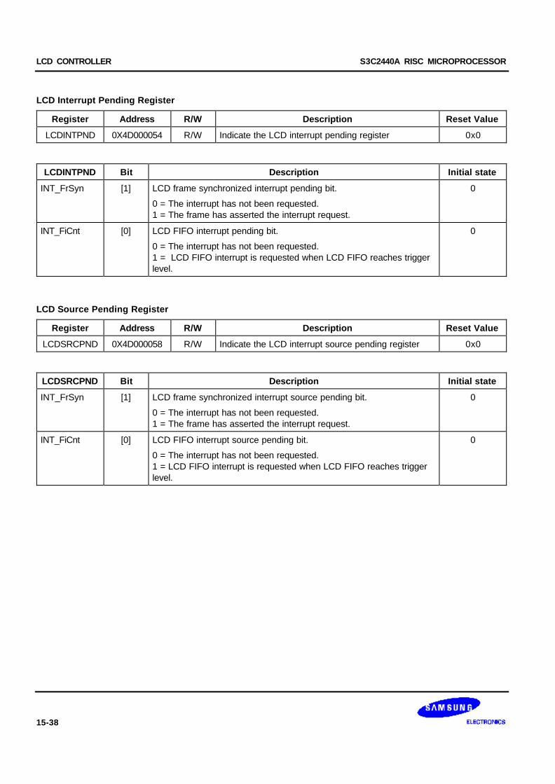
LCD CONTROLLER S3C2440A RISC MICROPROCESSOR
15-38
LCD Interrupt Pending Register
Register Address R/W Description Reset Value
LCDINTPND 0X4D000054 R/W Indicate the LCD interrupt pending register 0x0
LCDINTPND Bit Description Initial state
INT_FrSyn [1] LCD frame synchronized interrupt pending bit.
0 = The interrupt has not been requested.1 = The frame has asserted the interrupt request.
0
INT_FiCnt [0] LCD FIFO interrupt pending bit.
0 = The interrupt has not been requested.1 = LCD FIFO interrupt is requested when LCD FIFO reaches triggerlevel.
0
LCD Source Pending Register
Register Address R/W Description Reset Value
LCDSRCPND 0X4D000058 R/W Indicate the LCD interrupt source pending register 0x0
LCDSRCPND Bit Description Initial state
INT_FrSyn [1] LCD frame synchronized interrupt source pending bit.
0 = The interrupt has not been requested.1 = The frame has asserted the interrupt request.
0
INT_FiCnt [0] LCD FIFO interrupt source pending bit.
0 = The interrupt has not been requested.1 = LCD FIFO interrupt is requested when LCD FIFO reaches triggerlevel.
0

S3C2440A RISC MICROPROCESSOR LCD CONTROLLER
15-39
LCD Interrupt Mask Register
Register Address R/W Description Reset Value
LCDINTMSK 0X4D00005C R/W Determine which interrupt source is masked.The masked interrupt source will not be serviced.
0x3
LCDINTMSK Bit Description Initial state
FIWSEL [2] Determine the trigger level of LCD FIFO.
0 = 4 words 1 = 8 words
INT_FrSyn [1] Mask LCD frame synchronized interrupt.
0 = The interrupt service is available.1 = The interrupt service is masked.
1
INT_FiCnt [0] Mask LCD FIFO interrupt.
0 = The interrupt service is available.1 = The interrupt service is masked.
1
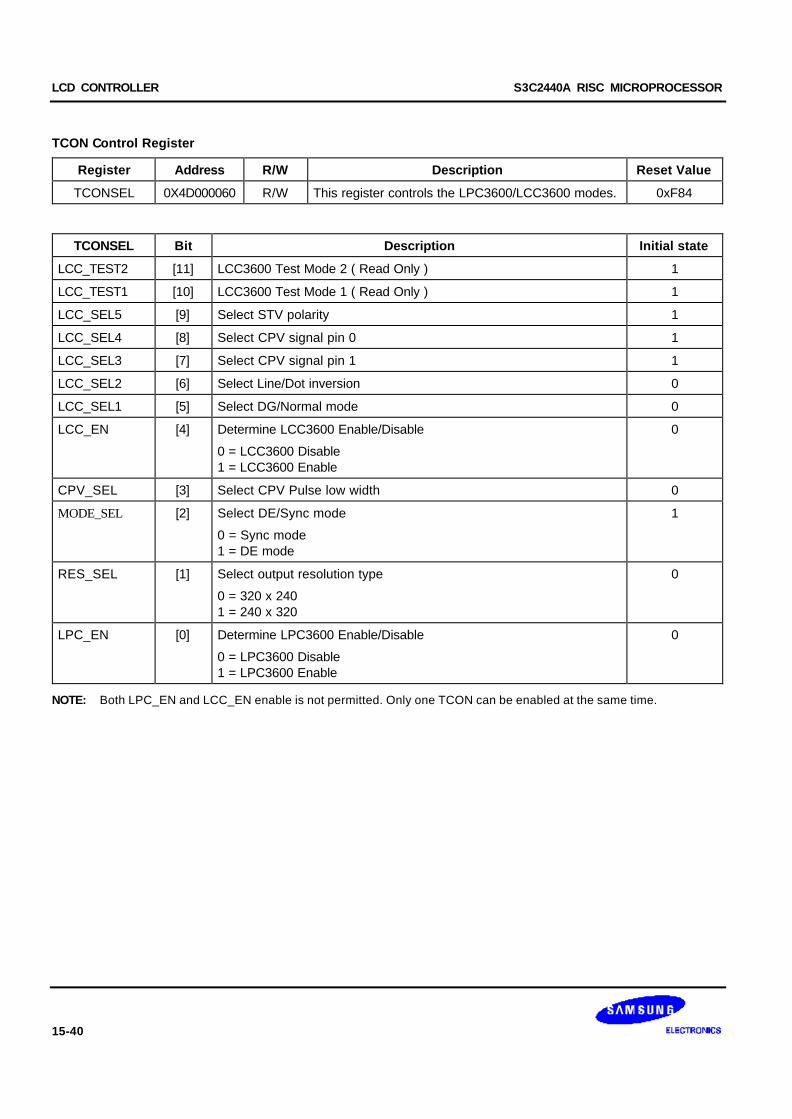
LCD CONTROLLER S3C2440A RISC MICROPROCESSOR
15-40
TCON Control Register
Register Address R/W Description Reset Value
TCONSEL 0X4D000060 R/W This register controls the LPC3600/LCC3600 modes. 0xF84
TCONSEL Bit Description Initial state
LCC_TEST2 [11] LCC3600 Test Mode 2 ( Read Only ) 1
LCC_TEST1 [10] LCC3600 Test Mode 1 ( Read Only ) 1
LCC_SEL5 [9] Select STV polarity 1
LCC_SEL4 [8] Select CPV signal pin 0 1
LCC_SEL3 [7] Select CPV signal pin 1 1
LCC_SEL2 [6] Select Line/Dot inversion 0
LCC_SEL1 [5] Select DG/Normal mode 0
LCC_EN [4] Determine LCC3600 Enable/Disable
0 = LCC3600 Disable1 = LCC3600 Enable
0
CPV_SEL [3] Select CPV Pulse low width 0
MODE_SEL [2] Select DE/Sync mode
0 = Sync mode1 = DE mode
1
RES_SEL [1] Select output resolution type
0 = 320 x 2401 = 240 x 320
0
LPC_EN [0] Determine LPC3600 Enable/Disable
0 = LPC3600 Disable1 = LPC3600 Enable
0
NOTE: Both LPC_EN and LCC_EN enable is not permitted. Only one TCON can be enabled at the same time.

S3C2440A RISC MICROPROCESSOR LCD CONTROLLER
15-41
Register Setting Guide (STN)
The LCD controller supports multiple screen sizes by special register setting.
The CLKVAL value determines the frequency of VCLK. This value has to be determined such that the VCLK value isgreater than data transmission rate. The data transmission rate for the VD port of the LCD controller is used todetermine the value of CLKVAL register.
The data transmission rate is given by the following equation:
Data transmission rate = HS x VS x FR x MV
— HS: Horizontal LCD size
— VS: Vertical LCD size
— FR: Frame rate
— MV: Mode dependent value
Table 15-6. MV Value for Each Display Mode
Mode MV Value
Mono, 4-bit single scan display 1/4
Mono, 8-bit single scan display or 4-bit dual scan display 1/8
4 level gray, 4-bit single scan display 1/4
4 level gray, 8-bit single scan display or 4-bit dual scan display 1/8
16 level gray, 4-bit single scan display 1/4
16 level gray, 8-bit single scan display or 4-bit dual scan display 1/8
Color, 4-bit single scan display 3/4
Color, 8-bit single scan display or 4-bit dual scan display 3/8
The LCDBASEU register value is the first address value of the frame buffer. The lowest 4 bits must be eliminated forburst 4 word access. The LCDBASEL register value depends on LCD size and LCDBASEU. The LCDBASEL value isgiven by the following equation:
— LCDBASEL = LCDBASEU + LCDBASEL offset
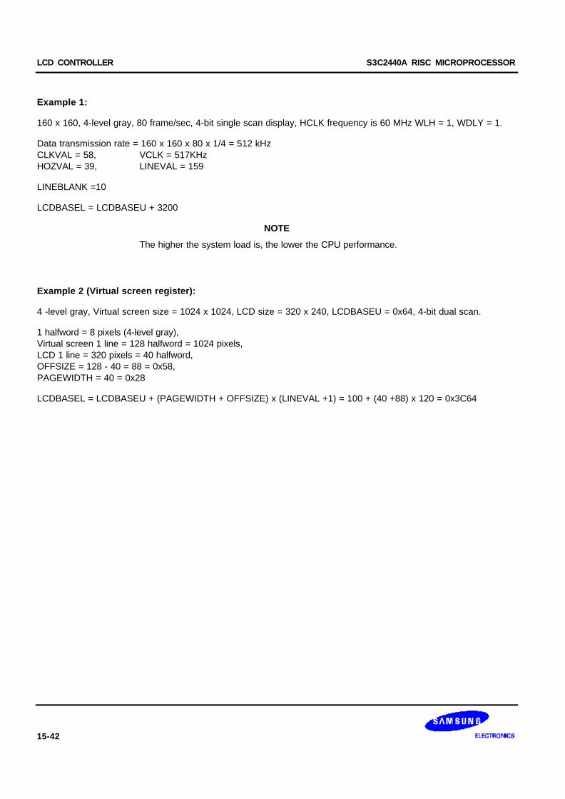
LCD CONTROLLER S3C2440A RISC MICROPROCESSOR
15-42
Example 1:
160 x 160, 4-level gray, 80 frame/sec, 4-bit single scan display, HCLK frequency is 60 MHz WLH = 1, WDLY = 1.
Data transmission rate = 160 x 160 x 80 x 1/4 = 512 kHzCLKVAL = 58, VCLK = 517KHzHOZVAL = 39, LINEVAL = 159
LINEBLANK =10
LCDBASEL = LCDBASEU + 3200
NOTE
The higher the system load is, the lower the CPU performance.
Example 2 (Virtual screen register):
4 -level gray, Virtual screen size = 1024 x 1024, LCD size = 320 x 240, LCDBASEU = 0x64, 4-bit dual scan.
1 halfword = 8 pixels (4-level gray),Virtual screen 1 line = 128 halfword = 1024 pixels,LCD 1 line = 320 pixels = 40 halfword,OFFSIZE = 128 - 40 = 88 = 0x58,PAGEWIDTH = 40 = 0x28
LCDBASEL = LCDBASEU + (PAGEWIDTH + OFFSIZE) x (LINEVAL +1) = 100 + (40 +88) x 120 = 0x3C64
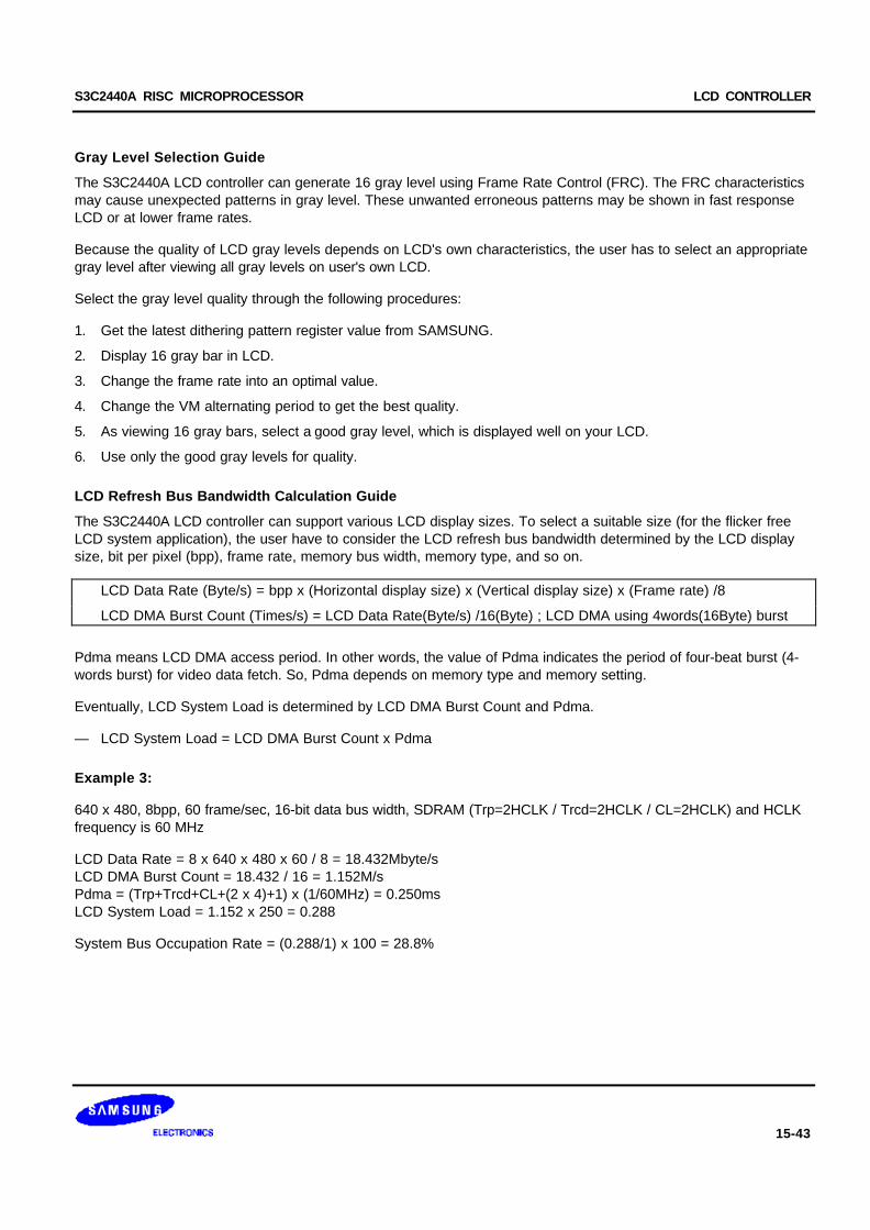
S3C2440A RISC MICROPROCESSOR LCD CONTROLLER
15-43
Gray Level Selection Guide
The S3C2440A LCD controller can generate 16 gray level using Frame Rate Control (FRC). The FRC characteristicsmay cause unexpected patterns in gray level. These unwanted erroneous patterns may be shown in fast responseLCD or at lower frame rates.
Because the quality of LCD gray levels depends on LCD's own characteristics, the user has to select an appropriategray level after viewing all gray levels on user's own LCD.
Select the gray level quality through the following procedures:
1. Get the latest dithering pattern register value from SAMSUNG.
2. Display 16 gray bar in LCD.
3. Change the frame rate into an optimal value.
4. Change the VM alternating period to get the best quality.
5. As viewing 16 gray bars, select a good gray level, which is displayed well on your LCD.
6. Use only the good gray levels for quality.
LCD Refresh Bus Bandwidth Calculation Guide
The S3C2440A LCD controller can support various LCD display sizes. To select a suitable size (for the flicker freeLCD system application), the user have to consider the LCD refresh bus bandwidth determined by the LCD displaysize, bit per pixel (bpp), frame rate, memory bus width, memory type, and so on.
LCD Data Rate (Byte/s) = bpp x (Horizontal display size) x (Vertical display size) x (Frame rate) /8
LCD DMA Burst Count (Times/s) = LCD Data Rate(Byte/s) /16(Byte) ; LCD DMA using 4words(16Byte) burst
Pdma means LCD DMA access period. In other words, the value of Pdma indicates the period of four-beat burst (4-words burst) for video data fetch. So, Pdma depends on memory type and memory setting.
Eventually, LCD System Load is determined by LCD DMA Burst Count and Pdma.
— LCD System Load = LCD DMA Burst Count x Pdma
Example 3:
640 x 480, 8bpp, 60 frame/sec, 16-bit data bus width, SDRAM (Trp=2HCLK / Trcd=2HCLK / CL=2HCLK) and HCLKfrequency is 60 MHz
LCD Data Rate = 8 x 640 x 480 x 60 / 8 = 18.432Mbyte/sLCD DMA Burst Count = 18.432 / 16 = 1.152M/sPdma = (Trp+Trcd+CL+(2 x 4)+1) x (1/60MHz) = 0.250msLCD System Load = 1.152 x 250 = 0.288
System Bus Occupation Rate = (0.288/1) x 100 = 28.8%
LCD CONTROLLER S3C2440A RISC MICROPROCESSOR
15-44
Register Setting Guide (TFT LCD)
The CLKVAL register value determines the frequency of VCLK and frame rate.
Frame Rate = 1/ [ (VSPW+1) + (VBPD+1) + (LIINEVAL + 1) + (VFPD+1) x (HSPW+1) + (HBPD +1) + (HFPD+1) + (HOZVAL + 1) x 2 x ( CLKVAL+1 ) / ( HCLK ) ]
For applications, the system timing must be considered to avoid under-run condition of the fifo of the lcd controllercaused by memory bandwidth contention.
Example 4:
TFT Resolution: 240 x 240,
VSPW =2, VBPD =14, LINEVAL = 239, VFPD =4
HSPW =25, HBPD =15, HOZVAL = 239, HFPD =1
CLKVAL = 5
HCLK = 60 M (hz)
The parameters below must be referenced by LCD size and driver specifications:
VSPW, VBPD, LINEVAL, VFPD, HSPW, HBPD, HOZVAL, and HFPD
If target frame rate is 60–70Hz, then CLKVAL should be 5.
So, Frame Rate = 67Hz
S3C2440A RISC MICROPROCESSOR ADC AND TOUCH SCREEN INTERFACE
16-1
16 ADC & TOUCH SCREEN INTERFACE
OVERVIEW
The 10-bit CMOS ADC (Analog to Digital Converter) is a recycling type device with 8-channel analog inputs. Itconverts the analog input signal into 10-bit binary digital codes at a maximum conversion rate of 500KSPS with2.5MHz A/D converter clock. A/D converter operates with on-chip sample-and-hold function and power down mode issupported.
Touch Screen Interface can control/select pads (XP, XM, YP, YM) of the Touch Screen for X, Y position conversion.Touch Screen Interface contains Touch Screen Pads control logic and ADC interface logic with an interruptgeneration logic.
FEATURES
— Resolution: 10-bit
— Differential Linearity Error: ± 1.0 LSB
— Integral Linearity Error: ± 2.0 LSB
— Maximum Conversion Rate: 500 KSPS
— Low Power Consumption
— Power Supply Voltage: 3.3V
— Analog Input Range: 0 ~ 3.3V
— On-chip sample-and-hold function
— Normal Conversion Mode
— Separate X/Y position conversion Mode
— Auto(Sequential) X/Y Position Conversion Mode
— Waiting for Interrupt Mode
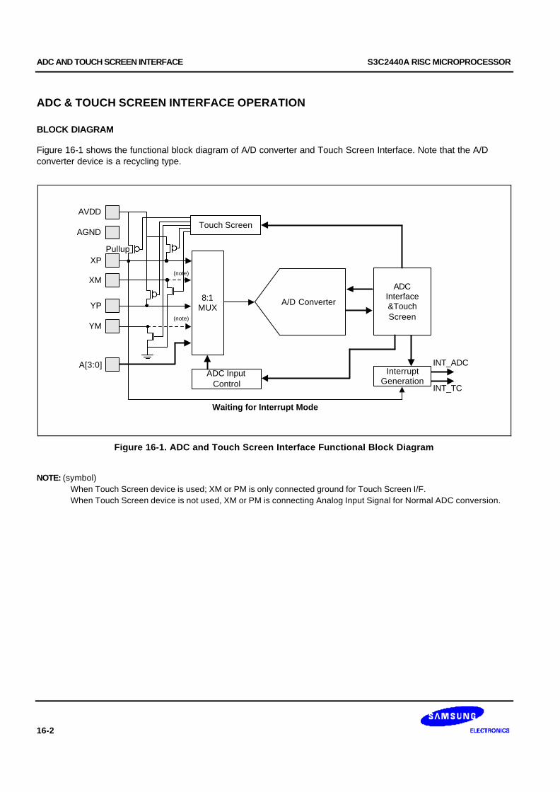
ADC AND TOUCH SCREEN INTERFACE S3C2440A RISC MICROPROCESSOR
16-2
ADC & TOUCH SCREEN INTERFACE OPERATION
BLOCK DIAGRAM
Figure 16-1 shows the functional block diagram of A/D converter and Touch Screen Interface. Note that the A/Dconverter device is a recycling type.
Pullup
Waiting for Interrupt Mode
INT_TC
INT_ADC
8:1MUX
A/D Converter
ADC InputControl
InterruptGeneration
ADCInterface&TouchScreen
AVDD
AGND
XP
XM
YP
YM
A[3:0]
(note)
(note)
Touch Screen
Figure 16-1. ADC and Touch Screen Interface Functional Block Diagram
NOTE: (symbol)When Touch Screen device is used; XM or PM is only connected ground for Touch Screen I/F. When Touch Screen device is not used, XM or PM is connecting Analog Input Signal for Normal ADC conversion.

S3C2440A RISC MICROPROCESSOR ADC AND TOUCH SCREEN INTERFACE
16-3
FUNCTION DESCRIPTIONS
A/D Conversion Time
When the GCLK frequency is 50MHz and the prescaler value is 49, total 10-bit conversion time is as follows.
A/D converter freq. = 50MHz/(49+1) = 1MHz
Conversion time = 1/(1MHz / 5cycles) = 1/200KHz = 5 us
NOTE
This A/D converter was designed to operate at maximum 2.5MHz clock, so the conversion rate can go up to500 KSPS.
Touch Screen Interface Mode
1. Normal Conversion Mode
Single Conversion Mode is the most likely used for General Purpose ADC Conversion. This mode can beinitialized by setting the ADCCON (ADC Control Register) and completed with a read and a write to theADCDAT0 (ADC Data Register 0).
2. Separate X/Y position conversion Mode
Touch Screen Controller can be operated by one of two Conversion Modes. Separate X/Y Position ConversionMode is operated as the following way. X-Position Mode writes X-Position Conversion Data to ADCDAT0, soTouch Screen Interface generates the Interrupt source to Interrupt Controller. Y-Position Mode writes Y-PositionConversion Data to ADCDAT1, so Touch Screen Interface generates the Interrupt source to Interrupt Controller.
3. Auto(Sequential) X/Y Position Conversion Mode
Auto (Sequential) X/Y Position Conversion Mode is operated as the following. Touch Screen Controllersequentially converts X-Position and Y-Position that is touched. After Touch controller writes X-measurementdata to ADCDAT0 and writes Y-measurement data to ADCDAT1, Touch Screen Interface is generating Interruptsource to Interrupt Controller in Auto Position Conversion Mode.
4. Waiting for Interrupt Mode
Touch Screen Controller generates interrupt (INT_TC) signal when the Stylus is down. Waiting for Interrupt Modesetting value is rADCTSC=0xd3; // XP_PU, XP_Dis, XM_Dis, YP_Dis, YM_En.
After Touch Screen Controller generates interrupt signal (INT_TC), Waiting for interrupt Mode must be cleared.(XY_PST sets to the No operation Mode)
Standby Mode
Standby mode is activated when ADCCON [2] is set to '1'. In this mode, A/D conversion operation is halted andADCDAT0, ADCDAT1 register contains the previous converted data.
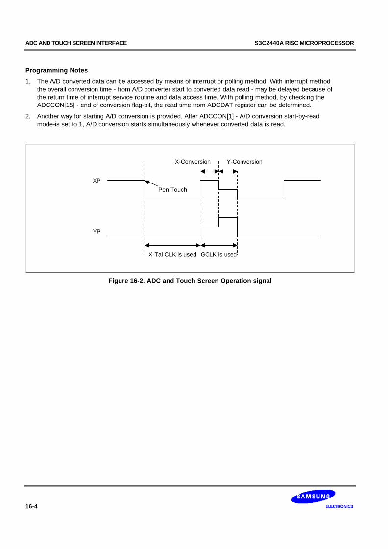
ADC AND TOUCH SCREEN INTERFACE S3C2440A RISC MICROPROCESSOR
16-4
Programming Notes
1. The A/D converted data can be accessed by means of interrupt or polling method. With interrupt methodthe overall conversion time - from A/D converter start to converted data read - may be delayed because ofthe return time of interrupt service routine and data access time. With polling method, by checking theADCCON[15] - end of conversion flag-bit, the read time from ADCDAT register can be determined.
2. Another way for starting A/D conversion is provided. After ADCCON[1] - A/D conversion start-by-readmode-is set to 1, A/D conversion starts simultaneously whenever converted data is read.
XP
X-Tal CLK is used
X-Conversion
YP
GCLK is used
Y-Conversion
Pen Touch
Figure 16-2. ADC and Touch Screen Operation signal
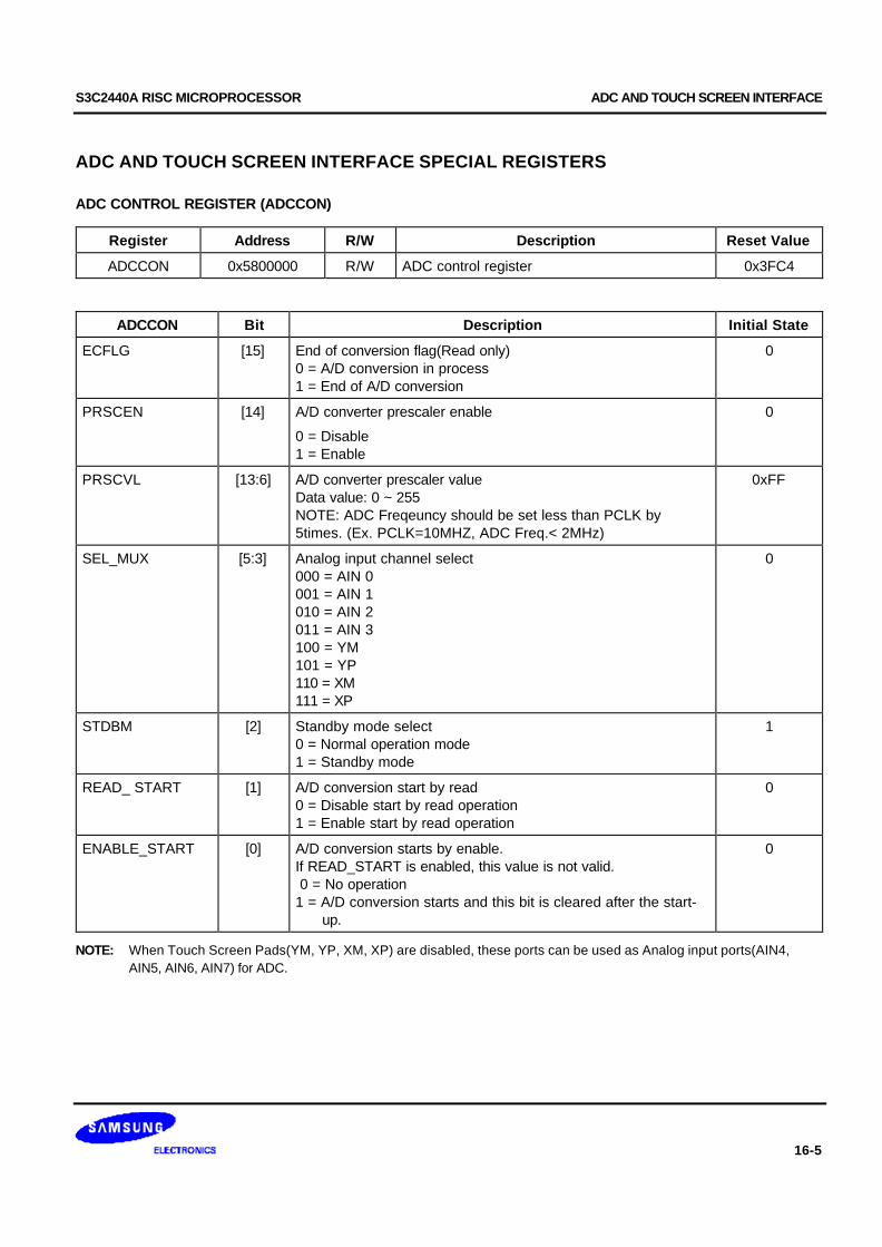
S3C2440A RISC MICROPROCESSOR ADC AND TOUCH SCREEN INTERFACE
16-5
ADC AND TOUCH SCREEN INTERFACE SPECIAL REGISTERS
ADC CONTROL REGISTER (ADCCON)
Register Address R/W Description Reset Value
ADCCON 0x5800000 R/W ADC control register 0x3FC4
ADCCON Bit Description Initial State
ECFLG [15] End of conversion flag(Read only)0 = A/D conversion in process1 = End of A/D conversion
0
PRSCEN [14] A/D converter prescaler enable
0 = Disable1 = Enable
0
PRSCVL [13:6] A/D converter prescaler valueData value: 0 ~ 255NOTE: ADC Freqeuncy should be set less than PCLK by5times. (Ex. PCLK=10MHZ, ADC Freq.< 2MHz)
0xFF
SEL_MUX [5:3] Analog input channel select000 = AIN 0001 = AIN 1010 = AIN 2011 = AIN 3100 = YM101 = YP110 = XM111 = XP
0
STDBM [2] Standby mode select0 = Normal operation mode1 = Standby mode
1
READ_ START [1] A/D conversion start by read0 = Disable start by read operation1 = Enable start by read operation
0
ENABLE_START [0] A/D conversion starts by enable.If READ_START is enabled, this value is not valid. 0 = No operation1 = A/D conversion starts and this bit is cleared after the start- up.
0
NOTE: When Touch Screen Pads(YM, YP, XM, XP) are disabled, these ports can be used as Analog input ports(AIN4, AIN5, AIN6, AIN7) for ADC.
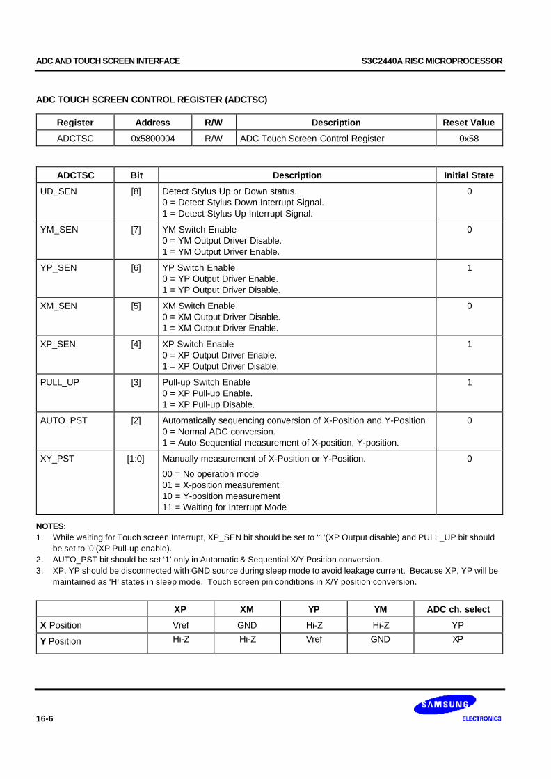
ADC AND TOUCH SCREEN INTERFACE S3C2440A RISC MICROPROCESSOR
16-6
ADC TOUCH SCREEN CONTROL REGISTER (ADCTSC)
Register Address R/W Description Reset Value
ADCTSC 0x5800004 R/W ADC Touch Screen Control Register 0x58
ADCTSC Bit Description Initial State
UD_SEN [8] Detect Stylus Up or Down status.0 = Detect Stylus Down Interrupt Signal.1 = Detect Stylus Up Interrupt Signal.
0
YM_SEN [7] YM Switch Enable0 = YM Output Driver Disable.1 = YM Output Driver Enable.
0
YP_SEN [6] YP Switch Enable0 = YP Output Driver Enable.1 = YP Output Driver Disable.
1
XM_SEN [5] XM Switch Enable0 = XM Output Driver Disable.1 = XM Output Driver Enable.
0
XP_SEN [4] XP Switch Enable0 = XP Output Driver Enable.1 = XP Output Driver Disable.
1
PULL_UP [3] Pull-up Switch Enable0 = XP Pull-up Enable.1 = XP Pull-up Disable.
1
AUTO_PST [2] Automatically sequencing conversion of X-Position and Y-Position0 = Normal ADC conversion.1 = Auto Sequential measurement of X-position, Y-position.
0
XY_PST [1:0] Manually measurement of X-Position or Y-Position.
00 = No operation mode01 = X-position measurement10 = Y-position measurement11 = Waiting for Interrupt Mode
0
NOTES:1. While waiting for Touch screen Interrupt, XP_SEN bit should be set to ‘1’(XP Output disable) and PULL_UP bit should
be set to ‘0’(XP Pull-up enable).2. AUTO_PST bit should be set ‘1’ only in Automatic & Sequential X/Y Position conversion.3. XP, YP should be disconnected with GND source during sleep mode to avoid leakage current. Because XP, YP will be maintained as 'H' states in sleep mode. Touch screen pin conditions in X/Y position conversion.
XP XM YP YM ADC ch. select
X Position Vref GND Hi-Z Hi-Z YP
Y Position Hi-Z Hi-Z Vref GND XP
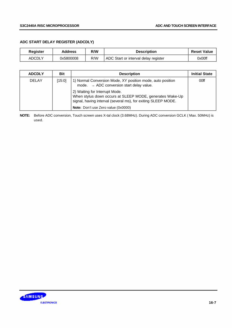
S3C2440A RISC MICROPROCESSOR ADC AND TOUCH SCREEN INTERFACE
16-7
ADC START DELAY REGISTER (ADCDLY)
Register Address R/W Description Reset Value
ADCDLY 0x5800008 R/W ADC Start or interval delay register 0x00ff
ADCDLY Bit Description Initial State
DELAY [15:0] 1) Normal Conversion Mode, XY position mode, auto positionmode. → ADC conversion start delay value.
2) Waiting for Interrupt Mode.When stylus down occurs at SLEEP MODE, generates Wake-Upsignal, having interval (several ms), for exiting SLEEP MODE.
Note: Don’t use Zero value (0x0000)
00ff
NOTE: Before ADC conversion, Touch screen uses X-tal clock (3.68MHz). During ADC conversion GCLK ( Max. 50MHz) is used.

ADC AND TOUCH SCREEN INTERFACE S3C2440A RISC MICROPROCESSOR
16-8
ADC CONVERSION DATA REGISTER (ADCDAT0)
Register Address R/W Description Reset Value
ADCDAT0 0x580000C R ADC conversion data register –
ADCDAT0 Bit Description Initial State
UPDOWN [15] Up or Down state of stylus at waiting for interrupt mode.
0 = Stylus down state.1 = Stylus up state.
–
AUTO_PST [14] Automatic sequencing conversion of X-position andY-Position
0 = Normal ADC conversion.1 = Sequencing measurement of X-position, Y-position.
–
XY_PST [13:12] Manually measurement of X-position or Y-position.
00 = No operation mode01 = X-position measurement10 = Y-position measurement11 = Waiting for Interrupt Mode
–
Reserved [11:10] Reserved –
XPDATA(Normal ADC)
[9:0] X-Position conversion data value (include normal ADC conversiondata value)Data value: 0 ~ 3FF
–
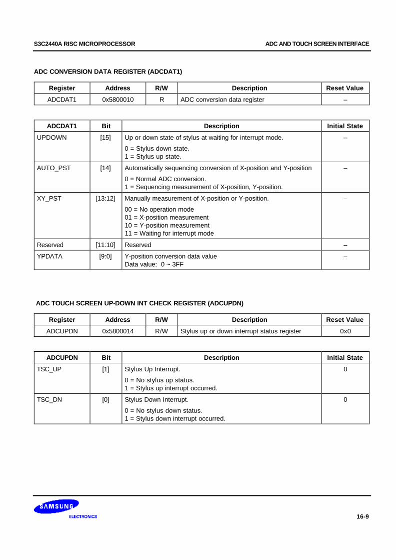
S3C2440A RISC MICROPROCESSOR ADC AND TOUCH SCREEN INTERFACE
16-9
ADC CONVERSION DATA REGISTER (ADCDAT1)
Register Address R/W Description Reset Value
ADCDAT1 0x5800010 R ADC conversion data register –
ADCDAT1 Bit Description Initial State
UPDOWN [15] Up or down state of stylus at waiting for interrupt mode.
0 = Stylus down state.1 = Stylus up state.
–
AUTO_PST [14] Automatically sequencing conversion of X-position and Y-position
0 = Normal ADC conversion.1 = Sequencing measurement of X-position, Y-position.
–
XY_PST [13:12] Manually measurement of X-position or Y-position.
00 = No operation mode01 = X-position measurement10 = Y-position measurement11 = Waiting for interrupt mode
–
Reserved [11:10] Reserved –
YPDATA [9:0] Y-position conversion data valueData value: 0 ~ 3FF
–
ADC TOUCH SCREEN UP-DOWN INT CHECK REGISTER (ADCUPDN)
Register Address R/W Description Reset Value
ADCUPDN 0x5800014 R/W Stylus up or down interrupt status register 0x0
ADCUPDN Bit Description Initial State
TSC_UP [1] Stylus Up Interrupt.
0 = No stylus up status.1 = Stylus up interrupt occurred.
0
TSC_DN [0] Stylus Down Interrupt.
0 = No stylus down status.1 = Stylus down interrupt occurred.
0

ADC AND TOUCH SCREEN INTERFACE S3C2440A RISC MICROPROCESSOR
16-10
NOTES

S3C2440A RISC MICROPROCESSOR REAL TIME CLOCK
17-1
17 REAL TIME CLOCK
OVERVIEW
The Real Time Clock (RTC) unit can be operated by the backup battery while the system power is off. The RTC cantransmit 8-bit data to CPU as Binary Coded Decimal (BCD) values using the STRB/LDRB ARM operation. The datainclude the time by second, minute, hour, date, day, month, and year. The RTC unit works with an external32.768kHz crystal and also can perform the alarm function.
FEATURES
— BCD number: second, minute, hour, date, day, month, and year
— Leap year generator
— Alarm function: alarm interrupt or wake-up from power-off mode
— Year 2000 problem is removed.
— Independent power pin (RTCVDD)
— Supports millisecond tick time interrupt for RTOS kernel time tick.
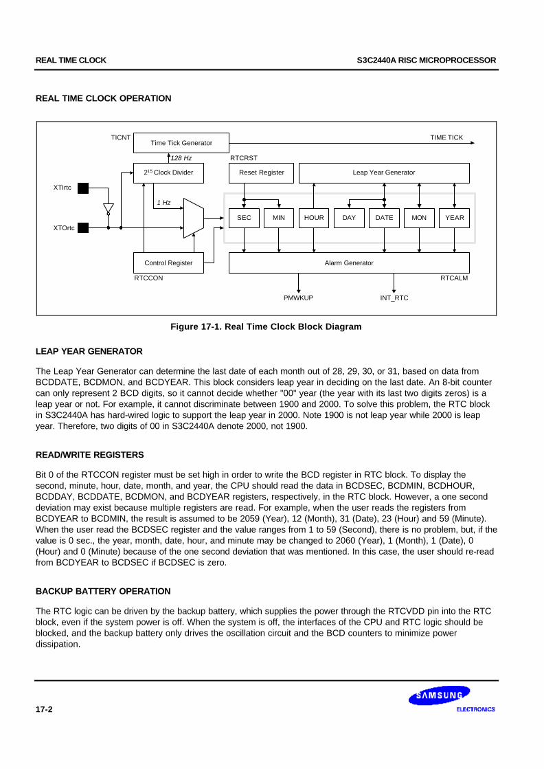
REAL TIME CLOCK S3C2440A RISC MICROPROCESSOR
17-2
REAL TIME CLOCK OPERATION
215 Clock Divider
XTOrtc
XTIrtc
Control Register
SEC MIN HOUR DAY DATE MON YEAR
Leap Year Generator
Alarm Generator
Reset Register
1 Hz
INT_RTC
RTCCON RTCALM
RTCRST
Time Tick GeneratorTIME TICKTICNT
128 Hz
PMWKUP
Figure 17-1. Real Time Clock Block Diagram
LEAP YEAR GENERATOR
The Leap Year Generator can determine the last date of each month out of 28, 29, 30, or 31, based on data fromBCDDATE, BCDMON, and BCDYEAR. This block considers leap year in deciding on the last date. An 8-bit countercan only represent 2 BCD digits, so it cannot decide whether "00" year (the year with its last two digits zeros) is aleap year or not. For example, it cannot discriminate between 1900 and 2000. To solve this problem, the RTC blockin S3C2440A has hard-wired logic to support the leap year in 2000. Note 1900 is not leap year while 2000 is leapyear. Therefore, two digits of 00 in S3C2440A denote 2000, not 1900.
READ/WRITE REGISTERS
Bit 0 of the RTCCON register must be set high in order to write the BCD register in RTC block. To display thesecond, minute, hour, date, month, and year, the CPU should read the data in BCDSEC, BCDMIN, BCDHOUR,BCDDAY, BCDDATE, BCDMON, and BCDYEAR registers, respectively, in the RTC block. However, a one seconddeviation may exist because multiple registers are read. For example, when the user reads the registers fromBCDYEAR to BCDMIN, the result is assumed to be 2059 (Year), 12 (Month), 31 (Date), 23 (Hour) and 59 (Minute).When the user read the BCDSEC register and the value ranges from 1 to 59 (Second), there is no problem, but, if thevalue is 0 sec., the year, month, date, hour, and minute may be changed to 2060 (Year), 1 (Month), 1 (Date), 0(Hour) and 0 (Minute) because of the one second deviation that was mentioned. In this case, the user should re-readfrom BCDYEAR to BCDSEC if BCDSEC is zero.
BACKUP BATTERY OPERATION
The RTC logic can be driven by the backup battery, which supplies the power through the RTCVDD pin into the RTCblock, even if the system power is off. When the system is off, the interfaces of the CPU and RTC logic should beblocked, and the backup battery only drives the oscillation circuit and the BCD counters to minimize powerdissipation.
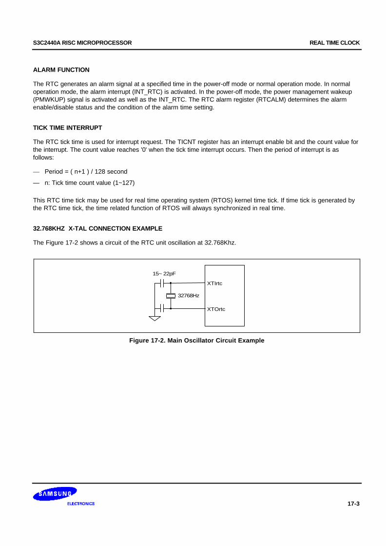
S3C2440A RISC MICROPROCESSOR REAL TIME CLOCK
17-3
ALARM FUNCTION
The RTC generates an alarm signal at a specified time in the power-off mode or normal operation mode. In normaloperation mode, the alarm interrupt (INT_RTC) is activated. In the power-off mode, the power management wakeup(PMWKUP) signal is activated as well as the INT_RTC. The RTC alarm register (RTCALM) determines the alarmenable/disable status and the condition of the alarm time setting.
TICK TIME INTERRUPT
The RTC tick time is used for interrupt request. The TICNT register has an interrupt enable bit and the count value forthe interrupt. The count value reaches '0' when the tick time interrupt occurs. Then the period of interrupt is asfollows:
— Period = ( n+1 ) / 128 second
— n: Tick time count value (1~127)
This RTC time tick may be used for real time operating system (RTOS) kernel time tick. If time tick is generated bythe RTC time tick, the time related function of RTOS will always synchronized in real time.
32.768KHZ X-TAL CONNECTION EXAMPLE
The Figure 17-2 shows a circuit of the RTC unit oscillation at 32.768Khz.
XTIrtc
XTOrtc
32768Hz
15~ 22pF
Figure 17-2. Main Oscillator Circuit Example

REAL TIME CLOCK S3C2440A RISC MICROPROCESSOR
17-4
REAL TIME CLOCK SPECIAL REGISTERS
REAL TIME CLOCK CONTROL (RTCCON) REGISTER
The RTCCON register consists of 4 bits such as the RTCEN, which controls the read/write enable of the BCDregisters, CLKSEL, CNTSEL, and CLKRST for testing.
RTCEN bit can control all interfaces between the CPU and the RTC, so it should be set to 1 in an RTC controlroutine to enable data read/write after a system reset. Also before power off, the RTCEN bit should be cleared to 0 toprevent inadvertent writing into RTC registers.
Register Address R/W Description Reset Value
RTCCON 0x57000040(L)0x57000043(B)
R/W(by byte)
RTC control register 0x0
RTCCON Bit Description Initial State
CLKRST [3] RTC clock count reset.0 = No reset, 1 = Reset
0
CNTSEL [2] BCD count select.0 = Merge BCD counters1 = Reserved (Separate BCD counters)
0
CLKSEL [1] BCD clock select.0 = XTAL 1/215 divided clock1 = Reserved (XTAL clock only for test)
0
RTCEN [0] RTC control enable.0 = Disable 1 = Enable
Note: Only BCD time count and read operation can be performed.
0
NOTES:1. All RTC registers have to be accessed for each byte unit using STRB and LDRB instructions or char type pointer.2. (L): Little endian.
(B): Big endian.
TICK TIME COUNT (TICNT) REGISTER
Register Address R/W Description Reset Value
TICNT 0x57000044(L)0x57000047(B)
R/W(by byte)
Tick time count register 0x0
TICNT Bit Description Initial State
TICK INT Enable [7] Tick time interrupt enable.0 = Disable 1 = Enable
0
TICK Time Count [6:0] Tick time count value (1~127).This counter value decreases internally, and users cannot read thiscounter value in working.
000000

S3C2440A RISC MICROPROCESSOR REAL TIME CLOCK
17-5
RTC ALARM CONTROL (RTCALM) REGISTER
The RTCALM register determines the alarm enable and the alarm time. Please note that the RTCALM registergenerates the alarm signal through both INT_RTC and PMWKUP in power down mode, but only through INT_RTC inthe normal operation mode.
Register Address R/W Description Reset Value
RTCALM 0x57000050(L)0x57000053(B)
R/W(by byte)
RTC alarm control register 0x0
RTCALM Bit Description Initial State
Reserved [7] – 0
ALMEN [6] Alarm global enable.0 = Disable, 1 = Enable
0
YEAREN [5] Year alarm enable.0 = Disable, 1 = Enable
0
MONREN [4] Month alarm enable.0 = Disable, 1 = Enable
0
DATEEN [3] Date alarm enable.0 = Disable, 1 = Enable
0
HOUREN [2] Hour alarm enable.0 = Disable, 1 = Enable
0
MINEN [1] Minute alarm enable.0 = Disable, 1 = Enable
0
SECEN [0] Second alarm enable.0 = Disable, 1 = Enable
0
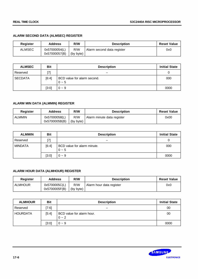
REAL TIME CLOCK S3C2440A RISC MICROPROCESSOR
17-6
ALARM SECOND DATA (ALMSEC) REGISTER
Register Address R/W Description Reset Value
ALMSEC 0x57000054(L)0x57000057(B)
R/W(by byte)
Alarm second data register 0x0
ALMSEC Bit Description Initial State
Reserved [7] – 0
SECDATA [6:4] BCD value for alarm second.0 ~ 5
000
[3:0] 0 ~ 9 0000
ALARM MIN DATA (ALMMIN) REGISTER
Register Address R/W Description Reset Value
ALMMIN 0x57000058(L)0x5700005B(B)
R/W(by byte)
Alarm minute data register 0x00
ALMMIN Bit Description Initial State
Reserved [7] – 0
MINDATA [6:4] BCD value for alarm minute.0 ~ 5
000
[3:0] 0 ~ 9 0000
ALARM HOUR DATA (ALMHOUR) REGISTER
Register Address R/W Description Reset Value
ALMHOUR 0x5700005C(L)0x5700005F(B)
R/W(by byte)
Alarm hour data register 0x0
ALMHOUR Bit Description Initial State
Reserved [7:6] – 00
HOURDATA [5:4] BCD value for alarm hour.0 ~ 2
00
[3:0] 0 ~ 9 0000

S3C2440A RISC MICROPROCESSOR REAL TIME CLOCK
17-7
ALARM DATE DATA (ALMDATE) REGISTER
Register Address R/W Description Reset Value
ALMDATE 0x57000060(L)0x57000063(B)
R/W(by byte)
Alarm date data register 0x01
ALMDATE Bit Description Initial State
Reserved [7:6] – 00
DATEDATA [5:4] BCD value for alarm date, from 0 to 28, 29, 30, 31.0 ~ 3
00
[3:0] 0 ~ 9 0001
ALARM MON DATA (ALMMON) REGISTER
Register Address R/W Description Reset Value
ALMMON 0x57000064(L)0x57000067(B)
R/W(by byte)
Alarm month data register 0x01
ALMMON Bit Description Initial State
Reserved [7:5] – 00
MONDATA [4] BCD value for alarm month.0 ~ 1
0
[3:0] 0 ~ 9 0001
ALARM YEAR DATA (ALMYEAR) REGISTER
Register Address R/W Description Reset Value
ALMYEAR 0x57000068(L)0x5700006B(B)
R/W(by byte)
Alarm year data register 0x0
ALMYEAR Bit Description Initial State
YEARDATA [7:0] BCD value for year.00 ~ 99
0x0
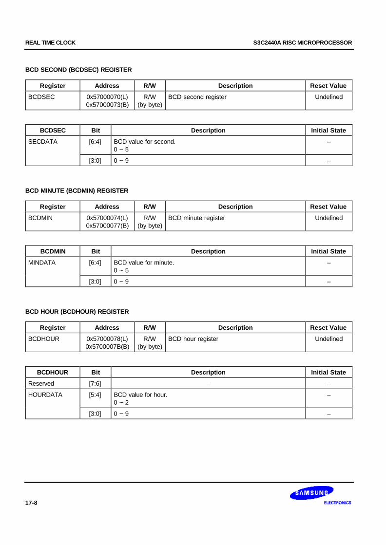
REAL TIME CLOCK S3C2440A RISC MICROPROCESSOR
17-8
BCD SECOND (BCDSEC) REGISTER
Register Address R/W Description Reset Value
BCDSEC 0x57000070(L)0x57000073(B)
R/W(by byte)
BCD second register Undefined
BCDSEC Bit Description Initial State
SECDATA [6:4] BCD value for second.0 ~ 5
–
[3:0] 0 ~ 9 –
BCD MINUTE (BCDMIN) REGISTER
Register Address R/W Description Reset Value
BCDMIN 0x57000074(L)0x57000077(B)
R/W(by byte)
BCD minute register Undefined
BCDMIN Bit Description Initial State
MINDATA [6:4] BCD value for minute.0 ~ 5
–
[3:0] 0 ~ 9 –
BCD HOUR (BCDHOUR) REGISTER
Register Address R/W Description Reset Value
BCDHOUR 0x57000078(L)0x5700007B(B)
R/W(by byte)
BCD hour register Undefined
BCDHOUR Bit Description Initial State
Reserved [7:6] – –
HOURDATA [5:4] BCD value for hour.0 ~ 2
–
[3:0] 0 ~ 9 –
S3C2440A RISC MICROPROCESSOR REAL TIME CLOCK
17-9
BCD DATE (BCDDATE) REGISTER
Register Address R/W Description Reset Value
BCDDATE 0x5700007C(L)0x5700007F(B)
R/W(by byte)
BCD date register Undefined
BCDDATE Bit Description Initial State
Reserved [7:6] – –
DATEDATA [5:4] BCD value for date.0 ~ 3
–
[3:0] 0 ~ 9 –
BCD DAY (BCDDAY) REGISTER
Register Address R/W Description Reset Value
BCDDAY 0x57000080(L)0x57000083(B)
R/W(by byte)
BCD a day of the week register Undefined
BCDDAY Bit Description Initial State
Reserved [7:3] – –
DAYDATA [2:0] BCD value for a day of the week.1 ~ 7
–
BCD MONTH (BCDMON) REGISTER
Register Address R/W Description Reset Value
BCDMON 0x57000084(L)0x57000087(B)
R/W(by byte)
BCD month register Undefined
BCDMON Bit Description Initial State
Reserved [7:5] – –
MONDATA [4] BCD value for month.0 ~ 1
–
[3:0] 0 ~ 9 –
REAL TIME CLOCK S3C2440A RISC MICROPROCESSOR
17-10
BCD YEAR (BCDYEAR) REGISTER
Register Address R/W Description Reset Value
BCDYEAR 0x57000088(L)0x5700008B(B)
R/W(by byte)
BCD year register Undefined
BCDYEAR Bit Description Initial State
YEARDATA [7:0] BCD value for year. 00 ~ 99
–
S3C2440A RISC MICROPROCESSOR WATCHDOG TIMER
18-1
18 WATCHDOG TIMER
OVERVIEW
The S3C2440A watchdog timer is used to resume the controller operation whenever it is disturbed by malfunctionssuch as noise and system errors. It can be used as a normal 16-bit interval timer to request interrupt service. Thewatchdog timer generates the reset signal for 128 PCLK cycles.
FEATURES
— Normal interval timer mode with interrupt request
— Internal reset signal is activated for 128 PCLK cycles when the timer count value reaches 0 (time-out).
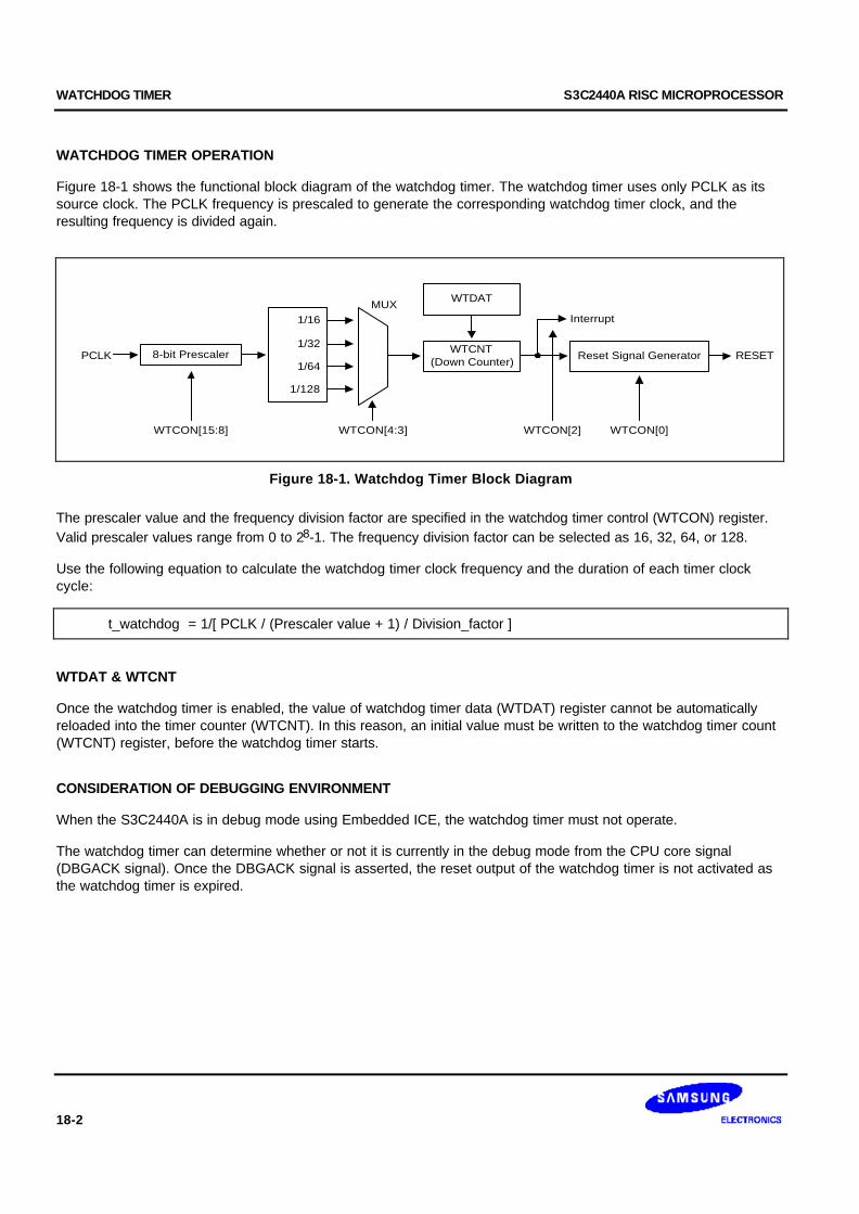
WATCHDOG TIMER S3C2440A RISC MICROPROCESSOR
18-2
WATCHDOG TIMER OPERATION
Figure 18-1 shows the functional block diagram of the watchdog timer. The watchdog timer uses only PCLK as itssource clock. The PCLK frequency is prescaled to generate the corresponding watchdog timer clock, and theresulting frequency is divided again.
Reset Signal GeneratorWTCNT
(Down Counter)PCLK
WTCON[4:3]
WTDAT
RESET
1/16
1/32
1/64
1/128
8-bit Prescaler
WTCON[15:8] WTCON[2] WTCON[0]
InterruptMUX
Figure 18-1. Watchdog Timer Block Diagram
The prescaler value and the frequency division factor are specified in the watchdog timer control (WTCON) register.Valid prescaler values range from 0 to 28-1. The frequency division factor can be selected as 16, 32, 64, or 128.
Use the following equation to calculate the watchdog timer clock frequency and the duration of each timer clockcycle:
t_watchdog = 1/[ PCLK / (Prescaler value + 1) / Division_factor ]
WTDAT & WTCNT
Once the watchdog timer is enabled, the value of watchdog timer data (WTDAT) register cannot be automaticallyreloaded into the timer counter (WTCNT). In this reason, an initial value must be written to the watchdog timer count(WTCNT) register, before the watchdog timer starts.
CONSIDERATION OF DEBUGGING ENVIRONMENT
When the S3C2440A is in debug mode using Embedded ICE, the watchdog timer must not operate.
The watchdog timer can determine whether or not it is currently in the debug mode from the CPU core signal(DBGACK signal). Once the DBGACK signal is asserted, the reset output of the watchdog timer is not activated asthe watchdog timer is expired.

S3C2440A RISC MICROPROCESSOR WATCHDOG TIMER
18-3
WATCHDOG TIMER SPECIAL REGISTERS
WATCHDOG TIMER CONTROL (WTCON) REGISTER
The WTCON register allows the user to enable/disable the watchdog timer, select the clock signal from 4 differentsources, enable/disable interrupts, and enable/disable the watchdog timer output. The Watchdog timer is used toresume the S3C2440A restart on mal-function after its power on; if controller restart is not desired, the Watchdogtimer should be disabled.
If the user wants to use the normal timer provided by the Watchdog timer, enable the interrupt and disable theWatchdog timer.
Register Address R/W Description Reset Value
WTCON 0x53000000 R/W Watchdog timer control register 0x8021
WTCON Bit Description Initial State
Prescaler value [15:8] Prescaler value.The valid range is from 0 to 255(28-1).
0x80
Reserved [7:6] Reserved.These two bits must be 00 in normal operation.
00
Watchdog timer [5] Enable or disable bit of Watchdog timer.0 = Disable1 = Enable
1
Clock select [4:3] Determine the clock division factor.
00: 16 01: 32
10: 64 11: 128
00
Interrupt generation [2] Enable or disable bit of the interrupt.0 = Disable1 = Enable
0
Reserved [1] Reserved.This bit must be 0 in normal operation.
0
Reset enable/disable [0] Enable or disable bit of Watchdog timer output for resetsignal.
1: Assert reset signal of the S3C2440A at watchdog time-out0: Disable the reset function of the watchdog timer.
1
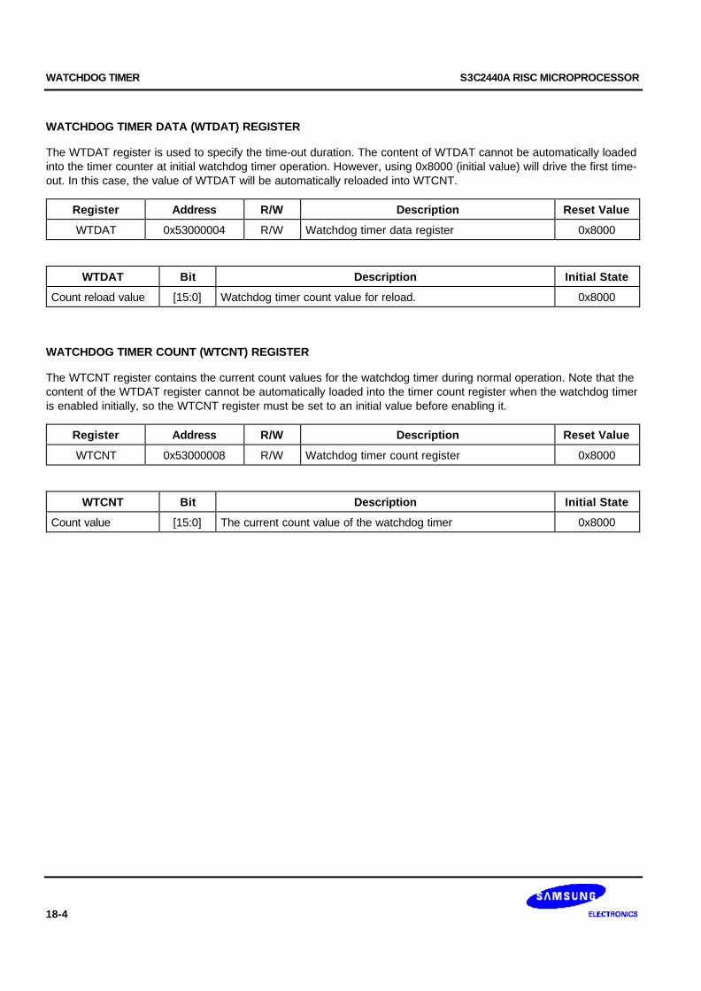
WATCHDOG TIMER S3C2440A RISC MICROPROCESSOR
18-4
WATCHDOG TIMER DATA (WTDAT) REGISTER
The WTDAT register is used to specify the time-out duration. The content of WTDAT cannot be automatically loadedinto the timer counter at initial watchdog timer operation. However, using 0x8000 (initial value) will drive the first time-out. In this case, the value of WTDAT will be automatically reloaded into WTCNT.
Register Address R/W Description Reset Value
WTDAT 0x53000004 R/W Watchdog timer data register 0x8000
WTDAT Bit Description Initial State
Count reload value [15:0] Watchdog timer count value for reload. 0x8000
WATCHDOG TIMER COUNT (WTCNT) REGISTER
The WTCNT register contains the current count values for the watchdog timer during normal operation. Note that thecontent of the WTDAT register cannot be automatically loaded into the timer count register when the watchdog timeris enabled initially, so the WTCNT register must be set to an initial value before enabling it.
Register Address R/W Description Reset Value
WTCNT 0x53000008 R/W Watchdog timer count register 0x8000
WTCNT Bit Description Initial State
Count value [15:0] The current count value of the watchdog timer 0x8000
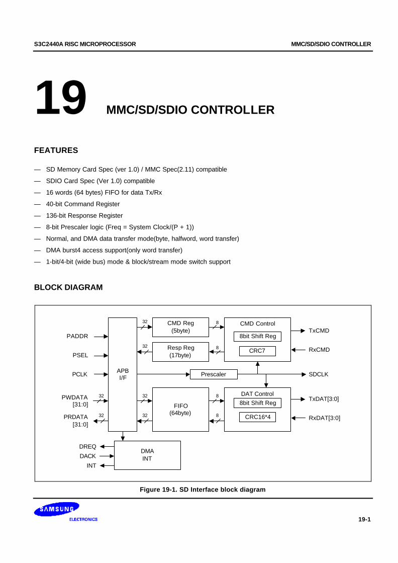
S3C2440A RISC MICROPROCESSOR MMC/SD/SDIO CONTROLLER
19-1
19 MMC/SD/SDIO CONTROLLER
FEATURES
— SD Memory Card Spec (ver 1.0) / MMC Spec(2.11) compatible
— SDIO Card Spec (Ver 1.0) compatible
— 16 words (64 bytes) FIFO for data Tx/Rx
— 40-bit Command Register
— 136-bit Response Register
— 8-bit Prescaler logic (Freq = System Clock/(P + 1))
— Normal, and DMA data transfer mode(byte, halfword, word transfer)
— DMA burst4 access support(only word transfer)
— 1-bit/4-bit (wide bus) mode & block/stream mode switch support
BLOCK DIAGRAM
CMD Reg(5byte)
Resp Reg(17byte)
CMD Control
8bit Shift Reg
CRC7
Prescaler
FIFO(64byte)
DAT Control8bit Shift Reg
CRC16*4
DMAINT
APBI/F
8
8
8
8
32
32
32
32
32
32
PADDR
PSEL
PCLK
PWDATA[31:0]
PRDATA[31:0]
DREQ
DACK
INT
TxCMD
RxCMD
SDCLK
TxDAT[3:0]
RxDAT[3:0]
Figure 19-1. SD Interface block diagram
MMC/SD/SDIO CONTROLLER S3C2440A RISC MICROPROCESSOR
19-2
SD OPERATION
A serial clock line synchronizes shifting and sampling of the information on the five data lines. The transmissionfrequency is controlled by making the appropriate bit settings to the SDIPRE register. You can modify its frequencyto adjust the baud rate data register value.
Programming Procedure (common)
To program the SDI modules, follow these basic steps:
1. Set SDICON to configure properly with clock & interrupt enable2. Set SDIPRE to configure with a proper value.3. Wait 74 SDCLK clock cycle in order to initialize the card.
CMD Path Programming
1. Write command argument 32bit to SDICmdArg.2. Determine command types and start command transmit with setting SDICmdCon.3. Confirm the end of SDI CMD path operation when the specific flag of SDICmdSta is set4. The flag is CmdSent if command type is no response.5. The flag is RspFin if command type is with response.6. Clear the flags of SDICmdSta by writing '1' to the corresponding bit.
DAT Path Programming
1. Write data timeout period to SDIDTimer.2. Write block size (block length) to SDIBSize(normally 0x80 word).3. Determine the mode of block, wide bus, dma, etc and start data transfer with setting SDIDatCon.4. Tx data → Write data to Data Register (SDIDAT) while Tx FIFO is available (TFDET is set), or half (TFHalf is set), or empty(TFEmpty is set).5. Rx data → Read data from Data Register (SDIDAT) while Rx FIFO is available (RFDET is set), or full (RFFull is set), or half (RFHalf is set), or ready for last data(RFLast is set).6. Confirm the end of SDI DAT path operation when DatFin flag of SDIDatSta is set7. Clear the flags of SDIDatSta by writing '1' to the corresponding bit.
S3C2440A RISC MICROPROCESSOR MMC/SD/SDIO CONTROLLER
19-3
SDIO OPERATION
There are two functions of SDIO operation: SDIO Interrupt receiving and Read Wait Request generation. These twofunctions can operate when RcvIOInt bit and RwaitEn bit of SDICON register is activated respectively. And twofunctions have the steps and conditions like below.
SDIO Interrupt
In SD 1-bit mode, Interrupt is received through all range from RxDAT[1] pin.
In SD 4-bit mode, RxDAT[1] pin is shared between data receiving and interrupt receiving.When interrupt detection range(Interrupt Period) is:
1. Single Block: The time between A and B– A: 2clocks after the completion of a data packet– B: The completion of sending the end bit of the next withdata command
2. Multi Block, PrdType = 0: The time between A and B, restart at C– A: 2clocks after the completion of a data packet– B: 2clocks after A– C: 2clocks after the end bit of the abort command response
3. Multi Block, PrdType = 1: The time between A and B, restart at A– A: 2clocks after the completion of a data packet– B: 2clocks after A– In case of last block, interrupt period begins at A, but not ends at B (CMD53 case)
Read Wait Request
Regardless of 1bit or 4-bit mode, Read Wait Request signal transmits to TxDAT[2] pin in condition of below.
— In read multiple operation, request signal transmission begins at 2clocks after the end of the data block
— Transmission ends when user sets to one RwaitReq bit of SDIDatSta register
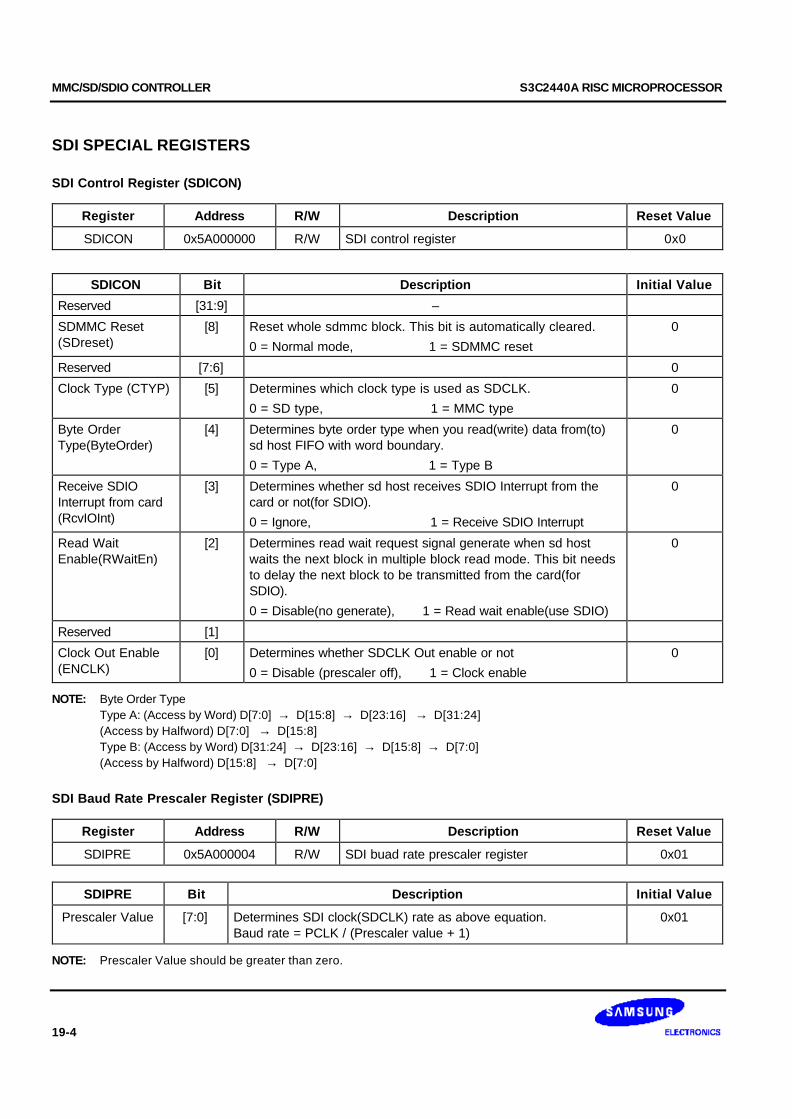
MMC/SD/SDIO CONTROLLER S3C2440A RISC MICROPROCESSOR
19-4
SDI SPECIAL REGISTERS
SDI Control Register (SDICON)
Register Address R/W Description Reset Value
SDICON 0x5A000000 R/W SDI control register 0x0
SDICON Bit Description Initial Value
Reserved [31:9] –
SDMMC Reset(SDreset)
[8] Reset whole sdmmc block. This bit is automatically cleared.
0 = Normal mode, 1 = SDMMC reset
0
Reserved [7:6] 0
Clock Type (CTYP) [5] Determines which clock type is used as SDCLK.
0 = SD type, 1 = MMC type
0
Byte OrderType(ByteOrder)
[4] Determines byte order type when you read(write) data from(to)sd host FIFO with word boundary.
0 = Type A, 1 = Type B
0
Receive SDIOInterrupt from card(RcvIOInt)
[3] Determines whether sd host receives SDIO Interrupt from thecard or not(for SDIO).
0 = Ignore, 1 = Receive SDIO Interrupt
0
Read WaitEnable(RWaitEn)
[2] Determines read wait request signal generate when sd hostwaits the next block in multiple block read mode. This bit needsto delay the next block to be transmitted from the card(forSDIO).
0 = Disable(no generate), 1 = Read wait enable(use SDIO)
0
Reserved [1]
Clock Out Enable(ENCLK)
[0] Determines whether SDCLK Out enable or not
0 = Disable (prescaler off), 1 = Clock enable
0
NOTE: Byte Order TypeType A: (Access by Word) D[7:0] → D[15:8] → D[23:16] → D[31:24](Access by Halfword) D[7:0] → D[15:8]Type B: (Access by Word) D[31:24] → D[23:16] → D[15:8] → D[7:0](Access by Halfword) D[15:8] → D[7:0]
SDI Baud Rate Prescaler Register (SDIPRE)
Register Address R/W Description Reset Value
SDIPRE 0x5A000004 R/W SDI buad rate prescaler register 0x01
SDIPRE Bit Description Initial Value
Prescaler Value [7:0] Determines SDI clock(SDCLK) rate as above equation.Baud rate = PCLK / (Prescaler value + 1)
0x01
NOTE: Prescaler Value should be greater than zero.

S3C2440A RISC MICROPROCESSOR MMC/SD/SDIO CONTROLLER
19-5
SDI Command Argument Register (SDICmdArg)
Register Address R/W Description Reset Value
SDICmdArg 0x5A000008 R/W SDI command argument register 0x0
SDICmdArg Bit Description Initial Value
CmdArg [31:0] Command argument 0x00000000
SDI Command Control Register (SDICmdCon)
Register Address R/W Description Reset Value
SDICmdCon 0x5A00000C R/W SDI command control register 0x0
SDICommand Bit Description Initial Value
Reserved [31:13] –
Abort Command(AbortCmd)
[12] Determines whether command type is for abort (for SDIO).
0 = Normal command, 1 = Abort command (CMD12, CMD52)
0
Command withData (WithData)
[11] Determines whether command type is with data(for SDIO).
0 = Without data, 1 = With data
0
LongRsp [10] Determines whether host receives a 136-bit long response or not
0 = Short response, 1 = Long response
0
WaitRsp [9] Determines whether host waits for a response or not
0 = No response, 1 = Wait response
0
CommandStart(CMST)
[8] Determines whether command operation starts or not. . This bit isautomatically cleared.
0 = Command ready, 1 = Command start
0
CmdIndex [7:0] Command index with start 2-bit (8-bit) 0x00
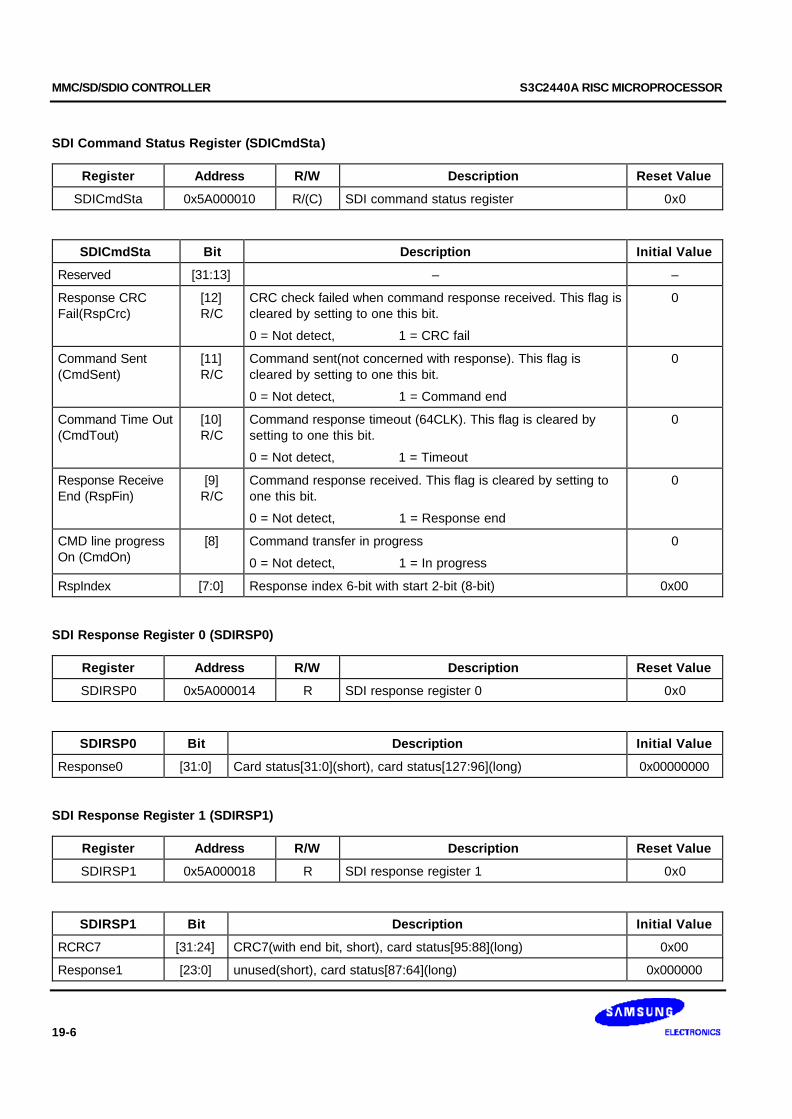
MMC/SD/SDIO CONTROLLER S3C2440A RISC MICROPROCESSOR
19-6
SDI Command Status Register (SDICmdSta)
Register Address R/W Description Reset Value
SDICmdSta 0x5A000010 R/(C) SDI command status register 0x0
SDICmdSta Bit Description Initial Value
Reserved [31:13] – –
Response CRCFail(RspCrc)
[12]R/C
CRC check failed when command response received. This flag iscleared by setting to one this bit.
0 = Not detect, 1 = CRC fail
0
Command Sent(CmdSent)
[11]R/C
Command sent(not concerned with response). This flag iscleared by setting to one this bit.
0 = Not detect, 1 = Command end
0
Command Time Out(CmdTout)
[10]R/C
Command response timeout (64CLK). This flag is cleared bysetting to one this bit.
0 = Not detect, 1 = Timeout
0
Response ReceiveEnd (RspFin)
[9]R/C
Command response received. This flag is cleared by setting toone this bit.
0 = Not detect, 1 = Response end
0
CMD line progressOn (CmdOn)
[8] Command transfer in progress
0 = Not detect, 1 = In progress
0
RspIndex [7:0] Response index 6-bit with start 2-bit (8-bit) 0x00
SDI Response Register 0 (SDIRSP0)
Register Address R/W Description Reset Value
SDIRSP0 0x5A000014 R SDI response register 0 0x0
SDIRSP0 Bit Description Initial Value
Response0 [31:0] Card status[31:0](short), card status[127:96](long) 0x00000000
SDI Response Register 1 (SDIRSP1)
Register Address R/W Description Reset Value
SDIRSP1 0x5A000018 R SDI response register 1 0x0
SDIRSP1 Bit Description Initial Value
RCRC7 [31:24] CRC7(with end bit, short), card status[95:88](long) 0x00
Response1 [23:0] unused(short), card status[87:64](long) 0x000000

S3C2440A RISC MICROPROCESSOR MMC/SD/SDIO CONTROLLER
19-7
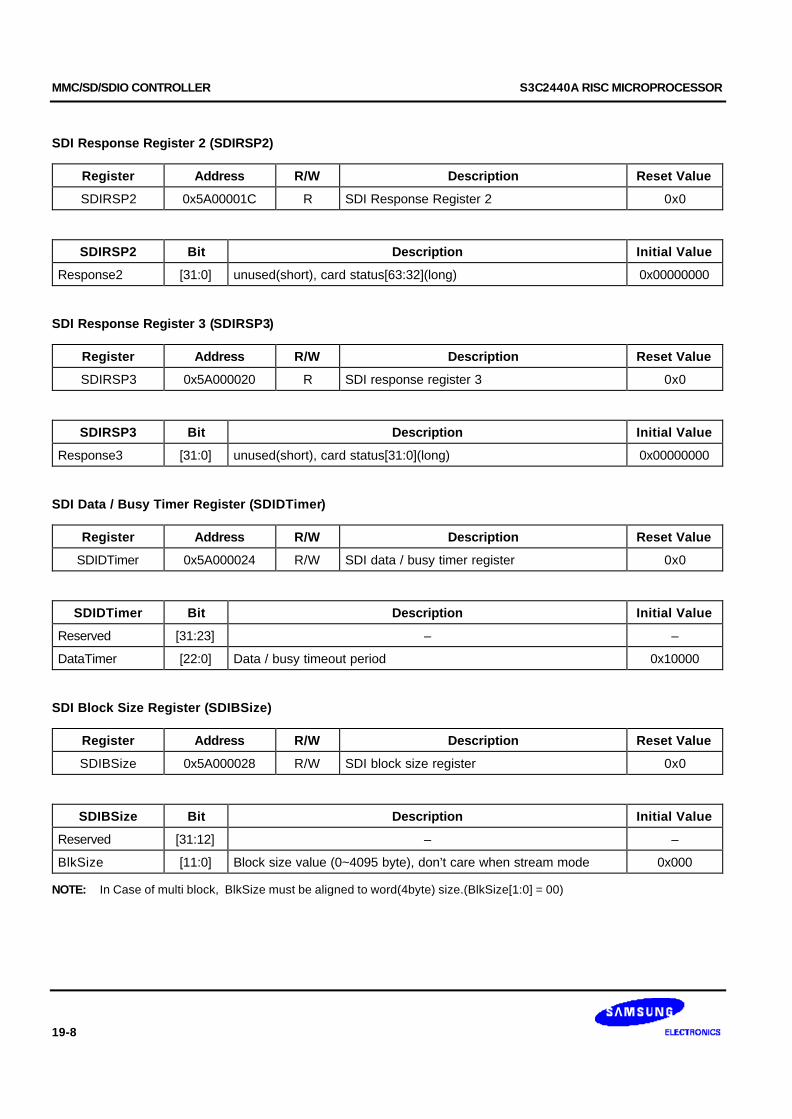
MMC/SD/SDIO CONTROLLER S3C2440A RISC MICROPROCESSOR
19-8
SDI Response Register 2 (SDIRSP2)
Register Address R/W Description Reset Value
SDIRSP2 0x5A00001C R SDI Response Register 2 0x0
SDIRSP2 Bit Description Initial Value
Response2 [31:0] unused(short), card status[63:32](long) 0x00000000
SDI Response Register 3 (SDIRSP3)
Register Address R/W Description Reset Value
SDIRSP3 0x5A000020 R SDI response register 3 0x0
SDIRSP3 Bit Description Initial Value
Response3 [31:0] unused(short), card status[31:0](long) 0x00000000
SDI Data / Busy Timer Register (SDIDTimer)
Register Address R/W Description Reset Value
SDIDTimer 0x5A000024 R/W SDI data / busy timer register 0x0
SDIDTimer Bit Description Initial Value
Reserved [31:23] – –
DataTimer [22:0] Data / busy timeout period 0x10000
SDI Block Size Register (SDIBSize)
Register Address R/W Description Reset Value
SDIBSize 0x5A000028 R/W SDI block size register 0x0
SDIBSize Bit Description Initial Value
Reserved [31:12] – –
BlkSize [11:0] Block size value (0~4095 byte), don’t care when stream mode 0x000
NOTE: In Case of multi block, BlkSize must be aligned to word(4byte) size.(BlkSize[1:0] = 00)

S3C2440A RISC MICROPROCESSOR MMC/SD/SDIO CONTROLLER
19-9
SDI Data Control Register (SDIDatCon)
Register Address R/W Description Reset Value
SDIDatCon 0x5A00002C R/W SDI data control register 0x0
SDIDatCon Bit Description Initial Value
Reserved [31:25] – –
Burst4 enable(Burst4)
[24] Enable Burst4 mode in DMA mode. This bit should be set onlywhen Data Size is word.0 = Disable, 1 = Burst4 enable
0
Data Size(DataSize)
[23:22] Indicates the size of the transfer with FIFO, which is typicallybyte, halfword or word.00 = Byte transfer, 01 = Halfword transfer10 = Word transfer, 11 = Reserved
0
SDIO InterruptPeriod Type(PrdType)
[21] Determines whether SDIO Interrupt period is 2 cycle or extendmore cycle when data block last is transferred (for SDIO).0 = Exactly 2 cycle, 1 = More cycle (likely singleblock)
0
Transmit AfterResponse (TARSP)
[20] Determines when data transmit start after response receive ornot0 = Directly after DatMode set,1 = After response receive (assume DatMode sets to 2’b11)
0
Receive AfterCommand(RACMD)
[19] Determines when data receive start after command sent or not0 = Directly after DatMode set,1 = After command sent (assume DatMode sets to 2’b10)
0
Busy AfterCommand(BACMD)
[18] Determines when busy receive start after command sent or not0 = Directly after DatMode set,1 = After command sent (assume DatMode sets to 2’b01)
0
Block mode(BlkMode)
[17] Data transfer mode0 = Stream data transfer, 1 = Block data transfer
0
Wide bus enable(WideBus)
[16] Determines enable wide bus mode0 = Standard bus mode(only SDIDAT[0] used),1 = Wide bus mode(SDIDAT[3:0] used)
0
DMA Enable(EnDMA)
[15] Enable DMA0 = Disable(polling), 1 = Dma enableWhen DMA operation is completed, this bit should be disabled.
0
Data TransferStart(DTST)
[14] Determines whether data transfer start or not. . This bit is auto-matically cleared.0 = Data ready, 1 = Data start
0
Data Transfer Mode(DatMode)
[13:12] Determines which direction of data transfer00 = No operation, 01 = Only busy check mode10 = Data receive mode, 11 = Data transmit mode
00
BlkNum [11:0] Block Number (0~4095), don’t care when stream mode 0x000
NOTE: If you want one of TARSP, RACMD, BACMD bits(SDIDatCon[20:18]) to “1”, you need to write on SDIDatCon register ahead of on SDICmdCon register.(always need for SDIO)

MMC/SD/SDIO CONTROLLER S3C2440A RISC MICROPROCESSOR
19-10
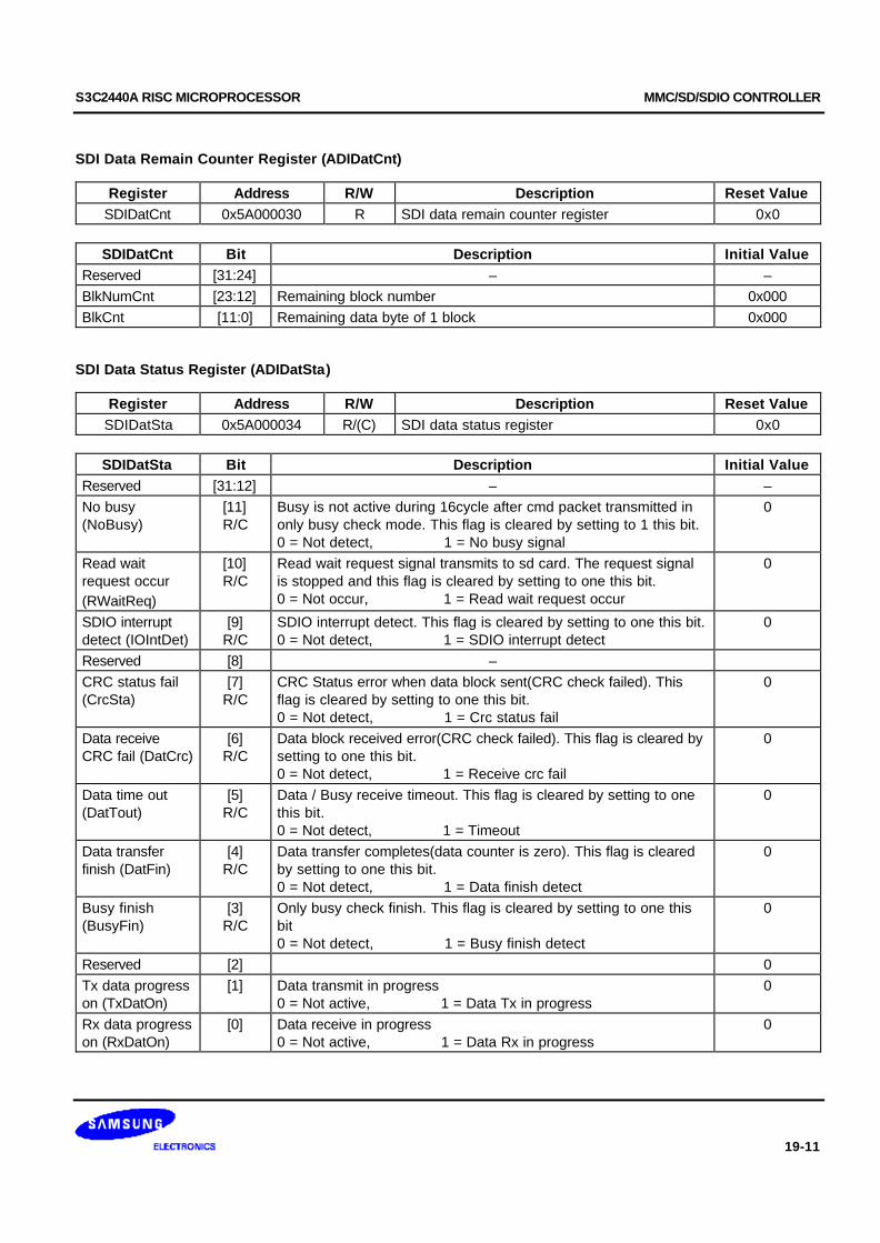
S3C2440A RISC MICROPROCESSOR MMC/SD/SDIO CONTROLLER
19-11
SDI Data Remain Counter Register (ADIDatCnt)
Register Address R/W Description Reset ValueSDIDatCnt 0x5A000030 R SDI data remain counter register 0x0
SDIDatCnt Bit Description Initial ValueReserved [31:24] – –BlkNumCnt [23:12] Remaining block number 0x000BlkCnt [11:0] Remaining data byte of 1 block 0x000
SDI Data Status Register (ADIDatSta)
Register Address R/W Description Reset ValueSDIDatSta 0x5A000034 R/(C) SDI data status register 0x0
SDIDatSta Bit Description Initial ValueReserved [31:12] – –No busy(NoBusy)
[11]R/C
Busy is not active during 16cycle after cmd packet transmitted inonly busy check mode. This flag is cleared by setting to 1 this bit.0 = Not detect, 1 = No busy signal
0
Read waitrequest occur(RWaitReq)
[10]R/C
Read wait request signal transmits to sd card. The request signalis stopped and this flag is cleared by setting to one this bit.0 = Not occur, 1 = Read wait request occur
0
SDIO interruptdetect (IOIntDet)
[9]R/C
SDIO interrupt detect. This flag is cleared by setting to one this bit.0 = Not detect, 1 = SDIO interrupt detect
0
Reserved [8] –CRC status fail(CrcSta)
[7]R/C
CRC Status error when data block sent(CRC check failed). Thisflag is cleared by setting to one this bit.0 = Not detect, 1 = Crc status fail
0
Data receiveCRC fail (DatCrc)
[6]R/C
Data block received error(CRC check failed). This flag is cleared bysetting to one this bit.0 = Not detect, 1 = Receive crc fail
0
Data time out(DatTout)
[5]R/C
Data / Busy receive timeout. This flag is cleared by setting to onethis bit.0 = Not detect, 1 = Timeout
0
Data transferfinish (DatFin)
[4]R/C
Data transfer completes(data counter is zero). This flag is clearedby setting to one this bit.0 = Not detect, 1 = Data finish detect
0
Busy finish(BusyFin)
[3]R/C
Only busy check finish. This flag is cleared by setting to one thisbit0 = Not detect, 1 = Busy finish detect
0
Reserved [2] 0Tx data progresson (TxDatOn)
[1] Data transmit in progress0 = Not active, 1 = Data Tx in progress
0
Rx data progresson (RxDatOn)
[0] Data receive in progress0 = Not active, 1 = Data Rx in progress
0
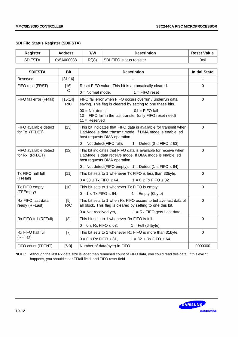
MMC/SD/SDIO CONTROLLER S3C2440A RISC MICROPROCESSOR
19-12
SDI Fifo Status Register (SDIFSTA)
Register Address R/W Description Reset Value
SDIFSTA 0x5A000038 R/(C) SDI FIFO status register 0x0
SDIFSTA Bit Description Initial State
Reserved [31:16] – –
FIFO reset(FRST) [16]C
Reset FIFO value. This bit is automatically cleared.
0 = Normal mode, 1 = FIFO reset
0
FIFO fail error (FFfail) [15:14]R/C
FIFO fail error when FIFO occurs overrun / underrun datasaving. This flag is cleared by setting to one these bits.
00 = Not detect, 01 = FIFO fail10 = FIFO fail in the last transfer (only FIFO reset need)11 = Reserved
0
FIFO available detectfor Tx (TFDET)
[13] This bit indicates that FIFO data is available for transmit whenDatMode is data transmit mode. If DMA mode is enable, sdhost requests DMA operation.
0 = Not detect(FIFO full), 1 = Detect (0 ≤ FIFO ≤ 63)
0
FIFO available detectfor Rx (RFDET)
[12] This bit indicates that FIFO data is available for receive whenDatMode is data receive mode. If DMA mode is enable, sdhost requests DMA operation.
0 = Not detect(FIFO empty), 1 = Detect (1 ≤ FIFO ≤ 64)
0
Tx FIFO half full(TFHalf)
[11] This bit sets to 1 whenever Tx FIFO is less than 33byte.
0 = 33 ≤ Tx FIFO ≤ 64, 1 = 0 ≤ Tx FIFO ≤ 32
0
Tx FIFO empty(TFEmpty)
[10] This bit sets to 1 whenever Tx FIFO is empty.
0 = 1 ≤ Tx FIFO ≤ 64, 1 = Empty (0byte)
0
Rx FIFO last dataready (RFLast)
[9]R/C
This bit sets to 1 when Rx FIFO occurs to behave last data ofall block. This flag is cleared by setting to one this bit.
0 = Not received yet, 1 = Rx FIFO gets Last data
0
Rx FIFO full (RFFull) [8] This bit sets to 1 whenever Rx FIFO is full.
0 = 0 ≤ Rx FIFO ≤ 63, 1 = Full (64byte)
0
Rx FIFO half full(RFHalf)
[7] This bit sets to 1 whenever Rx FIFO is more than 31byte.
0 = 0 ≤ Rx FIFO ≤ 31, 1 = 32 ≤ Rx FIFO ≤ 64
0
FIFO count (FFCNT) [6:0] Number of data(byte) in FIFO 0000000
NOTE: Although the last Rx data size is lager than remained count of FIFO data, you could read this data. If this event happens, you should clear FFfail field, and FIFO reset field
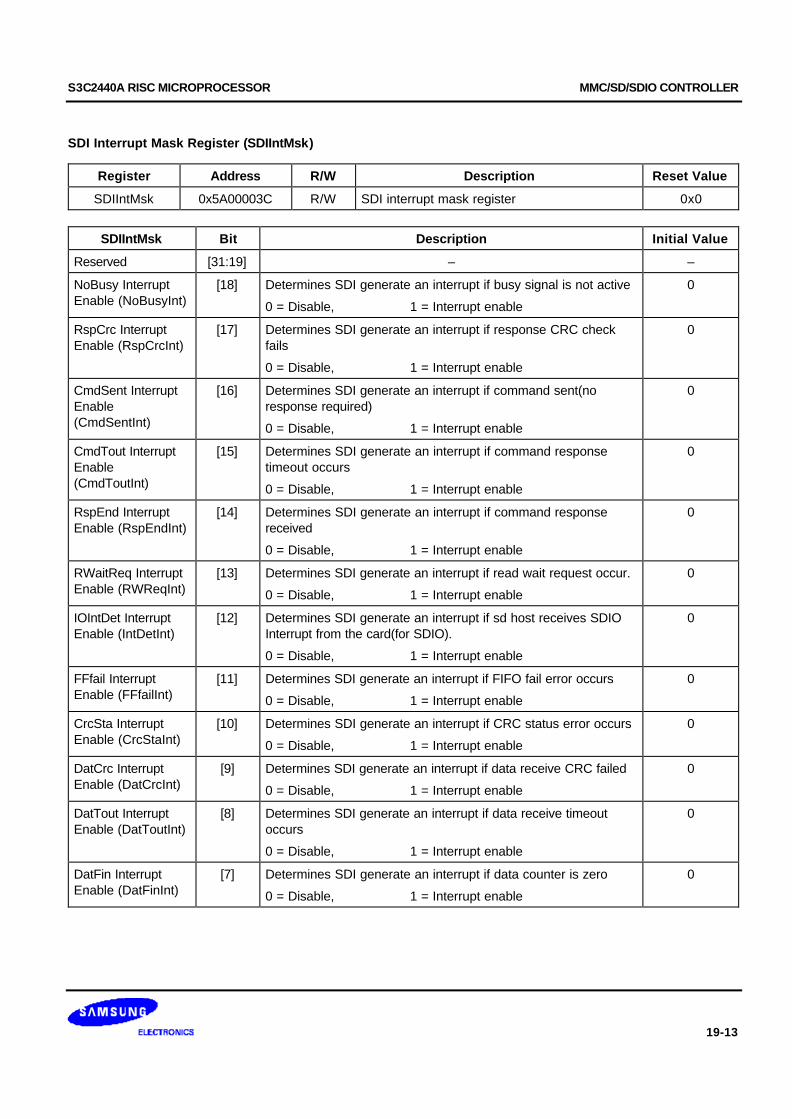
S3C2440A RISC MICROPROCESSOR MMC/SD/SDIO CONTROLLER
19-13
SDI Interrupt Mask Register (SDIIntMsk)
Register Address R/W Description Reset Value
SDIIntMsk 0x5A00003C R/W SDI interrupt mask register 0x0
SDIIntMsk Bit Description Initial Value
Reserved [31:19] – –
NoBusy InterruptEnable (NoBusyInt)
[18] Determines SDI generate an interrupt if busy signal is not active
0 = Disable, 1 = Interrupt enable
0
RspCrc InterruptEnable (RspCrcInt)
[17] Determines SDI generate an interrupt if response CRC checkfails
0 = Disable, 1 = Interrupt enable
0
CmdSent InterruptEnable(CmdSentInt)
[16] Determines SDI generate an interrupt if command sent(noresponse required)
0 = Disable, 1 = Interrupt enable
0
CmdTout InterruptEnable(CmdToutInt)
[15] Determines SDI generate an interrupt if command responsetimeout occurs
0 = Disable, 1 = Interrupt enable
0
RspEnd InterruptEnable (RspEndInt)
[14] Determines SDI generate an interrupt if command responsereceived
0 = Disable, 1 = Interrupt enable
0
RWaitReq InterruptEnable (RWReqInt)
[13] Determines SDI generate an interrupt if read wait request occur.
0 = Disable, 1 = Interrupt enable
0
IOIntDet InterruptEnable (IntDetInt)
[12] Determines SDI generate an interrupt if sd host receives SDIOInterrupt from the card(for SDIO).
0 = Disable, 1 = Interrupt enable
0
FFfail InterruptEnable (FFfailInt)
[11] Determines SDI generate an interrupt if FIFO fail error occurs
0 = Disable, 1 = Interrupt enable
0
CrcSta InterruptEnable (CrcStaInt)
[10] Determines SDI generate an interrupt if CRC status error occurs
0 = Disable, 1 = Interrupt enable
0
DatCrc InterruptEnable (DatCrcInt)
[9] Determines SDI generate an interrupt if data receive CRC failed
0 = Disable, 1 = Interrupt enable
0
DatTout InterruptEnable (DatToutInt)
[8] Determines SDI generate an interrupt if data receive timeoutoccurs
0 = Disable, 1 = Interrupt enable
0
DatFin InterruptEnable (DatFinInt)
[7] Determines SDI generate an interrupt if data counter is zero
0 = Disable, 1 = Interrupt enable
0

MMC/SD/SDIO CONTROLLER S3C2440A RISC MICROPROCESSOR
19-14
SDI Interrupt Mask Register (SDIIntMsk) (Continued)
SDIIntMsk Bit Description Initial Value
BusyFin InterruptEnable (BusyFinInt)
[6] Determines SDI generate an interrupt if only busy checkcompletes
0 = Disable, 1 = Interrupt enable
0
Reserved [5] – 0
TFHalf InterruptEnable (TFHalfInt)
[4] Determines SDI generate an interrupt if Tx FIFO fills half
0 = Disable, 1 = Interrupt enable
0
TFEmpty InterruptEnable (TFEmptInt)
[3] Determines SDI generate an interrupt if Tx FIFO is empty
0 = Disable, 1 = Interrupt enable
0
RFLast InterruptEnable (RFLastInt)
[2] Determines SDI generate an interrupt if Rx FIFO has last data
0 = Disable, 1 = Interrupt enable
0
RFFull InterruptEnable (RFFullInt)
[1] Determines SDI generate an interrupt if Rx FIFO fills full
0 = Disable, 1 = Interrupt enable
0
RFHalf InterruptEnable (RFHalfInt)
[0] Determines SDI generate an interrupt if Rx FIFO fills half
0 = Disable, 1 = Interrupt enable
0
SDI Data Register (SDIDAT)
Register Address R/W Description Reset Value
SDIDAT 0x5A000040, 44, 48,4C(Li/W, Li/HW, Li/B, Bi/W)
0x5A000041(Bi/HW),0x5A000043(Bi/B)
R/W SDI data register 0x0
SDIDAT Bit Description Initial State
Data Register [31:0] This field contains the data to be transmitted or received over theSDI channel
0x00000000
NOTE:— (Li/W, Li/HW, Li/B): Access by Word/HalfWord//Byte unit when endian mode is Little— (Bi/W): Access by Word unit when endian mode is Big— (Bi/HW): Access by HalfWord unit when endian mode is Big— (Bi/B): Access by Byte unit when endian mode is Big
S3C2440A RISC MICROPROCESSOR IIC-BUS INTERFACE
20-1
20 IIC-BUS INTERFACE
OVERVIEW
The S3C2440A RISC microprocessor can support a multi-master IIC-bus serial interface. A dedicated serial data line(SDA) and a serial clock line (SCL) carry information between bus masters and peripheral devices which areconnected to the IIC-bus. The SDA and SCL lines are bi-directional.
In multi-master IIC-bus mode, multiple S3C2440A RISC microprocessors can receive or transmit serial data to orfrom slave devices. The master S3C2440A can initiate and terminate a data transfer over the IIC-bus. The IIC-bus inthe S3C2440A uses Standard bus arbitration procedure.
To control multi-master IIC-bus operations, values must be written to the following registers:
— Multi-master IIC-bus control register, IICCON
— Multi-master IIC-bus control/status register, IICSTAT
— Multi-master IIC-bus Tx/Rx data shift register, IICDS
— Multi-master IIC-bus address register, IICADD
When the IIC-bus is free, the SDA and SCL lines should be both at High level. A High-to-Low transition of SDA caninitiate a Start condition. A Low-to-High transition of SDA can initiate a Stop condition while SCL remains steady atHigh Level.
The Start and Stop conditions can always be generated by the master devices. A 7-bit address value in the first databyte, which is put onto the bus after the Start condition has been initiated, can determine the slave device which thebus master device has selected. The 8th bit determines the direction of the transfer (read or write).
Every data byte put onto the SDA line should be eight bits in total. The bytes can be unlimitedly sent or receivedduring the bus transfer operation. Data is always sent from most-significant bit (MSB) first, and every byte should beimmediately followed by acknowledge (ACK) bit.
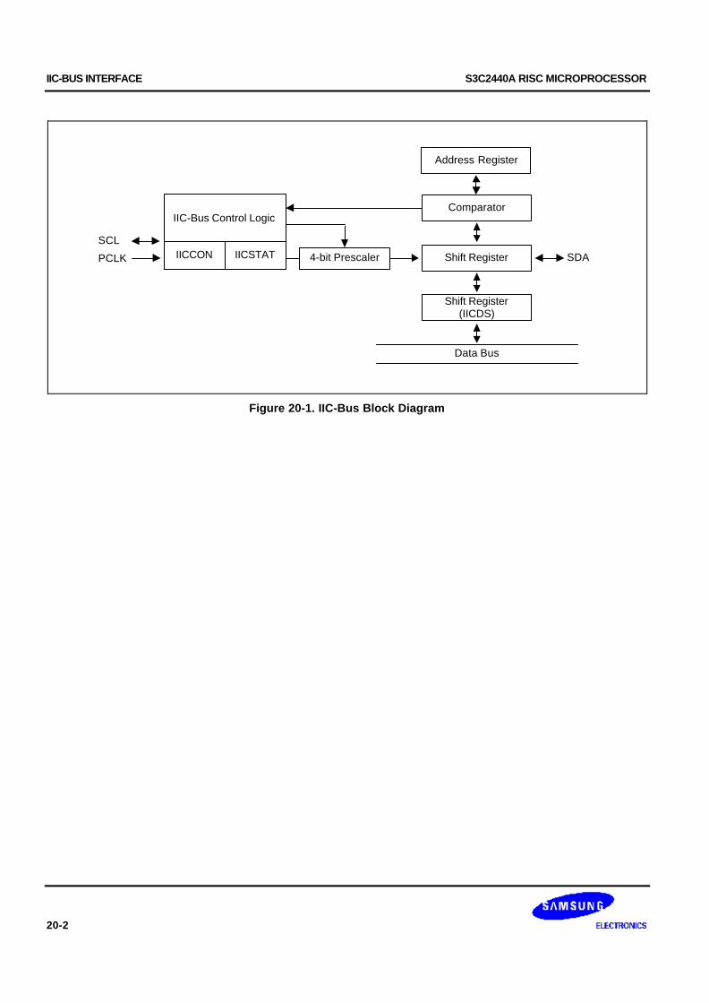
IIC-BUS INTERFACE S3C2440A RISC MICROPROCESSOR
20-2
PCLK
Address Register
SDA4-bit Prescaler
IIC-Bus Control Logic
IICSTATIICCON
Comparator
Shift Register
Shift Register(IICDS)
Data Bus
SCL
Figure 20-1. IIC-Bus Block Diagram
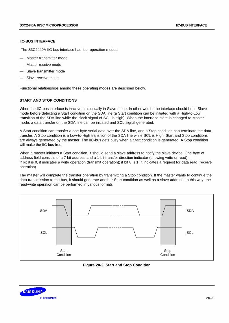
S3C2440A RISC MICROPROCESSOR IIC-BUS INTERFACE
20-3
IIC-BUS INTERFACE
The S3C2440A IIC-bus interface has four operation modes:
— Master transmitter mode
— Master receive mode
— Slave transmitter mode
— Slave receive mode
Functional relationships among these operating modes are described below.
START AND STOP CONDITIONS
When the IIC-bus interface is inactive, it is usually in Slave mode. In other words, the interface should be in Slavemode before detecting a Start condition on the SDA line (a Start condition can be initiated with a High-to-Lowtransition of the SDA line while the clock signal of SCL is High). When the interface state is changed to Mastermode, a data transfer on the SDA line can be initiated and SCL signal generated.
A Start condition can transfer a one-byte serial data over the SDA line, and a Stop condition can terminate the datatransfer. A Stop condition is a Low-to-High transition of the SDA line while SCL is High. Start and Stop conditionsare always generated by the master. The IIC-bus gets busy when a Start condition is generated. A Stop conditionwill make the IIC-bus free.
When a master initiates a Start condition, it should send a slave address to notify the slave device. One byte ofaddress field consists of a 7-bit address and a 1-bit transfer direction indicator (showing write or read).If bit 8 is 0, it indicates a write operation (transmit operation); if bit 8 is 1, it indicates a request for data read (receiveoperation).
The master will complete the transfer operation by transmitting a Stop condition. If the master wants to continue thedata transmission to the bus, it should generate another Start condition as well as a slave address. In this way, theread-write operation can be performed in various formats.
SCL
SDA SDA
SCL
StartCondition
StopCondition
Figure 20-2. Start and Stop Condition

IIC-BUS INTERFACE S3C2440A RISC MICROPROCESSOR
20-4
DATA TRANSFER FORMAT
Every byte placed on the SDA line should be eight bits in length. The bytes can be unlimitedly transmitted pertransfer. The first byte following a Start condition should have the address field. The address field can be transmittedby the master when the IIC-bus is operating in Master mode. Each byte should be followed by an acknowledgement(ACK) bit. The MSB bit of the serial data and addresses are always sent first.
NOTES:1. S: Start, rS: Repeat Start, P: Stop, A: Acknowledge2. : From Master to Slave, : From Slave to Master
Write Mode Format with 7-bit Addresses
"0"(Write) Data Transferred
(Data + Acknowledge)
S Slave Address 7bits R/W A PDATA(1Byte) A
Read Mode Format with 7-bit Addresses
"1"(Read) Data Transferred
(Data + Acknowledge)
S Slave Address 7 bits R/W A PDATA A
Write Mode Format with 10-bit Addresses
"0"(Write) Data Transferred
(Data + Acknowledge)
PDATA AS Slave Address1st 7 bits R/W A Slave Address
2nd Byte A
11110XX
Read Mode Format with 10-bit Addresses
"1"(Read)
S Slave Address1st 7 bits
11110XX
R/W A Slave Address2nd Byte
A rS Slave Address1st 7 Bits
A
Data Transferred(Data + Acknowledge)
PDATA AR/W
"1"(Read)
Figure 20-3. IIC-Bus Interface Data Format
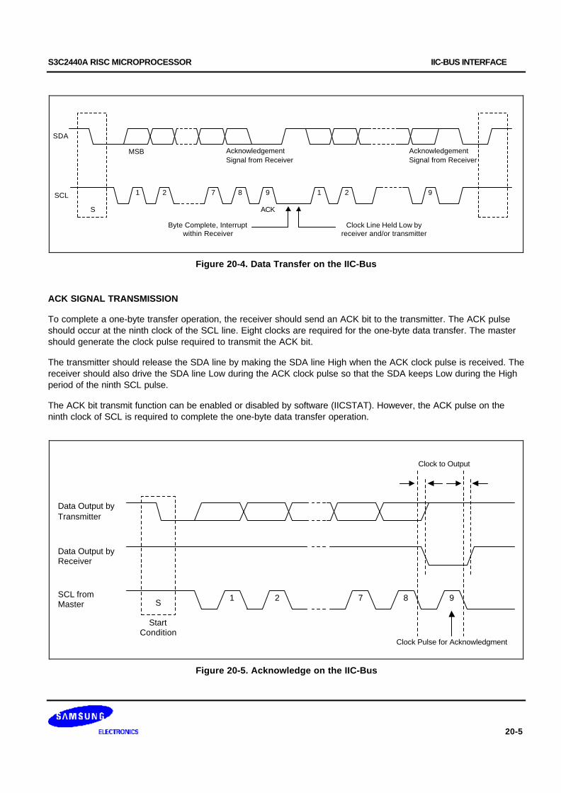
S3C2440A RISC MICROPROCESSOR IIC-BUS INTERFACE
20-5
SDA
AcknowledgementSignal from Receiver
SCL
S
1 2 7 8 9 1 2 9
AcknowledgementSignal from Receiver
MSB
ACK
Byte Complete, Interruptwithin Receiver
Clock Line Held Low byreceiver and/or transmitter
Figure 20-4. Data Transfer on the IIC-Bus
ACK SIGNAL TRANSMISSION
To complete a one-byte transfer operation, the receiver should send an ACK bit to the transmitter. The ACK pulseshould occur at the ninth clock of the SCL line. Eight clocks are required for the one-byte data transfer. The mastershould generate the clock pulse required to transmit the ACK bit.
The transmitter should release the SDA line by making the SDA line High when the ACK clock pulse is received. Thereceiver should also drive the SDA line Low during the ACK clock pulse so that the SDA keeps Low during the Highperiod of the ninth SCL pulse.
The ACK bit transmit function can be enabled or disabled by software (IICSTAT). However, the ACK pulse on theninth clock of SCL is required to complete the one-byte data transfer operation.
Data Output byTransmitter
Data Output byReceiver
SCL fromMaster
StartCondition
Clock Pulse for Acknowledgment
Clock to Output
987S 1 2
Figure 20-5. Acknowledge on the IIC-Bus
IIC-BUS INTERFACE S3C2440A RISC MICROPROCESSOR
20-6
READ-WRITE OPERATION
In Transmitter mode, when the data is transferred, the IIC-bus interface will wait until IIC-bus Data Shift (IICDS)register receives a new data. Before the new data is written into the register, the SCL line will be held low, and thenreleased after it is written. The S3C2440A should hold the interrupt to identify the completion of current data transfer.After the CPU receives the interrupt request, it should write a new data into the IICDS register, again.
In Receive mode, when data is received, the IIC-bus interface will wait until IICDS register is read. Before the newdata is read out, the SCL line will be held low and then released after it is read. The S3C2440A should hold theinterrupt to identify the completion of the new data reception. After the CPU receives the interrupt request, it shouldread the data from the IICDS register.
BUS ARBITRATION PROCEDURES
Arbitration takes place on the SDA line to prevent the contention on the bus between two masters. If a master with aSDA High level detects the other master with a SDA active Low level, it will not initiate a data transfer because thecurrent level on the bus does not correspond to its own. The arbitration procedure will be extended until the SDA lineturns High.
However, when the masters simultaneously lower the SDA line, each master should evaluate whether the mastershipis allocated itself or not. For the purpose of evaluation is that each master should detect the address bits. Whileeach master generates the slaver address, it should also detect the address bit on the SDA line because the SDAline is likely to get Low rather than to keep High. Assume that one master generates a Low as first address bit, whilethe other master is maintaining High. In this case, both masters will detect Low on the bus because the Low statusis superior to the High status in power. When this happens, Low (as the first bit of address) generating master willget the mastership while High (as the first bit of address) generating master should withdraw the mastership. If bothmasters generate Low as the first bit of address, there should be arbitration for the second address bit, again. Thisarbitration will continue to the end of last address bit.
ABORT CONDITIONS
If a slave receiver cannot acknowledge the confirmation of the slave address, it should hold the level of the SDA lineHigh. In this case, the master should generate a Stop condition and to abort the transfer.
If a master receiver is involved in the aborted transfer, it should signal the end of the slave transmit operation bycanceling the generation of an ACK after the last data byte received from the slave. The slave transmitter should thenrelease the SDA to allow a master to generate a Stop condition.
CONFIGURING IIC-BUS
To control the frequency of the serial clock (SCL), the 4-bit prescaler value can be programmed in the IICCONregister. The IIC-bus interface address is stored in the IIC-bus address (IICADD) register. (By default, the IIC-businterface address has an unknown value.)
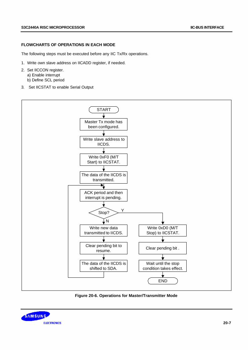
S3C2440A RISC MICROPROCESSOR IIC-BUS INTERFACE
20-7
FLOWCHARTS OF OPERATIONS IN EACH MODE
The following steps must be executed before any IIC Tx/Rx operations.
1. Write own slave address on IICADD register, if needed.
2. Set IICCON register.a) Enable interruptb) Define SCL period
3. Set IICSTAT to enable Serial Output
Write slave address toIICDS.
Write 0xF0 (M/TStart) to IICSTAT.
The data of the IICDS istransmitted.
ACK period and theninterrupt is pending.
Write 0xD0 (M/TStop) to IICSTAT.
Write new datatransmitted to IICDS.
Stop?
Clear pending bit toresume.
The data of the IICDS isshifted to SDA.
START
Master Tx mode hasbeen configured.
Clear pending bit .
Wait until the stopcondition takes effect.
END
Y
N
Figure 20-6. Operations for Master/Transmitter Mode

IIC-BUS INTERFACE S3C2440A RISC MICROPROCESSOR
20-8
Write slave address toIICDS.
Write 0xB0 (M/RStart) to IICSTAT.
The data of the IICDS (slaveaddress) is transmitted.
ACK period and theninterrupt is pending.
Write 0x90 (M/RStop) to IICSTAT.
Read a new data fromIICDS.
Stop?
Clear pending bit toresume.
SDA is shifted to IICDS.
START
Master Rx mode hasbeen configured.
Clear pending bit .
Wait until the stopcondition takes effect.
END
Y
N
Figure 20-7. Operations for Master/Receiver Mode

S3C2440A RISC MICROPROCESSOR IIC-BUS INTERFACE
20-9
IIC detects start signal. and, IICDSreceives data.
IIC compares IICADD and IICDS (thereceived slave address).
Write data to IICDS.
The IIC address matchinterrupt is generated.
Clear pending bit toresume.
The data of the IICDS isshifted to SDA.
START
Slave Tx mode hasbeen configured.
END
Matched?
N
Y
Stop?
Interrupt is pending.
N
Y
Figure 20-8. Operations for Slave/Transmitter Mode

IIC-BUS INTERFACE S3C2440A RISC MICROPROCESSOR
20-10
IIC detects start signal. and, IICDSreceives data.
IIC compares IICADD and IICDS (thereceived slave address).
Read data from IICDS.
The IIC address matchinterrupt is generated.
Clear pending bit toresume.
SDA is shifted to IICDS.
START
Slave Rx mode hasbeen configured.
END
Matched?
N
Y
Stop?
Interrupt is pending.
N
Y
Figure 20-9. Operations for Slave/Receiver Mode
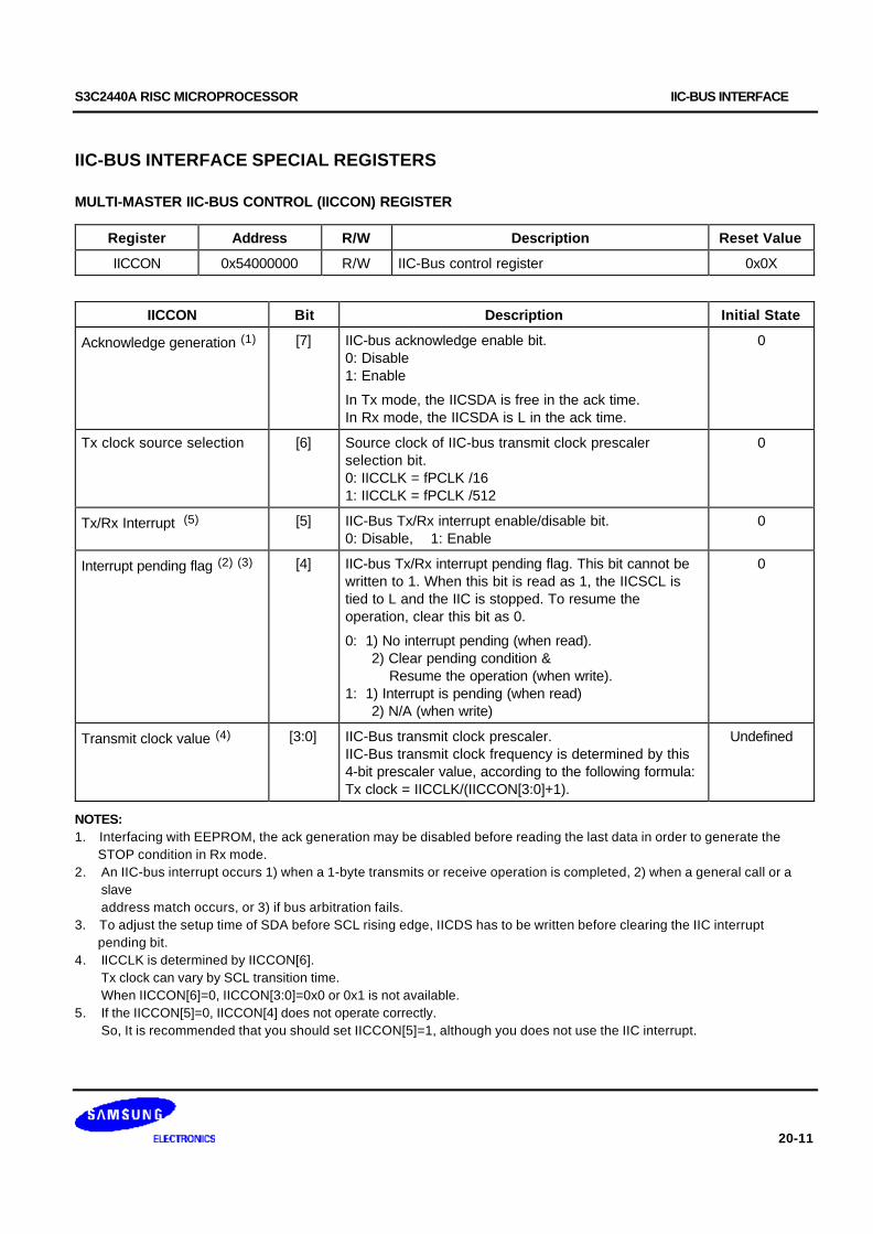
S3C2440A RISC MICROPROCESSOR IIC-BUS INTERFACE
20-11
IIC-BUS INTERFACE SPECIAL REGISTERS
MULTI-MASTER IIC-BUS CONTROL (IICCON) REGISTER
Register Address R/W Description Reset Value
IICCON 0x54000000 R/W IIC-Bus control register 0x0X
IICCON Bit Description Initial State
Acknowledge generation (1) [7] IIC-bus acknowledge enable bit.0: Disable1: Enable
In Tx mode, the IICSDA is free in the ack time.In Rx mode, the IICSDA is L in the ack time.
0
Tx clock source selection [6] Source clock of IIC-bus transmit clock prescalerselection bit.0: IICCLK = fPCLK /161: IICCLK = fPCLK /512
0
Tx/Rx Interrupt (5) [5] IIC-Bus Tx/Rx interrupt enable/disable bit.0: Disable, 1: Enable
0
Interrupt pending flag (2) (3) [4] IIC-bus Tx/Rx interrupt pending flag. This bit cannot bewritten to 1. When this bit is read as 1, the IICSCL istied to L and the IIC is stopped. To resume theoperation, clear this bit as 0.
0: 1) No interrupt pending (when read). 2) Clear pending condition & Resume the operation (when write).1: 1) Interrupt is pending (when read) 2) N/A (when write)
0
Transmit clock value (4) [3:0] IIC-Bus transmit clock prescaler.IIC-Bus transmit clock frequency is determined by this4-bit prescaler value, according to the following formula:Tx clock = IICCLK/(IICCON[3:0]+1).
Undefined
NOTES:1. Interfacing with EEPROM, the ack generation may be disabled before reading the last data in order to generate the STOP condition in Rx mode.2. An IIC-bus interrupt occurs 1) when a 1-byte transmits or receive operation is completed, 2) when a general call or a
slave address match occurs, or 3) if bus arbitration fails.3. To adjust the setup time of SDA before SCL rising edge, IICDS has to be written before clearing the IIC interrupt pending bit.4. IICCLK is determined by IICCON[6]. Tx clock can vary by SCL transition time. When IICCON[6]=0, IICCON[3:0]=0x0 or 0x1 is not available.5. If the IICCON[5]=0, IICCON[4] does not operate correctly. So, It is recommended that you should set IICCON[5]=1, although you does not use the IIC interrupt.

IIC-BUS INTERFACE S3C2440A RISC MICROPROCESSOR
20-12
MULTI-MASTER IIC-BUS CONTROL/STATUS (IICSTAT) REGISTER
Register Address R/W Description Reset Value
IICSTAT 0x54000004 R/W IIC-Bus control/status register 0x0
IICSTAT Bit Description Initial State
Mode selection [7:6] IIC-bus master/slave Tx/Rx mode select bits.
00: Slave receive mode01: Slave transmit mode10: Master receive mode11: Master transmit mode
00
Busy signal status /
START STOP condition
[5] IIC-Bus busy signal status bit.
0: read) Not busy (when read) write) STOP signal generation1: read) Busy (when read) write) START signal generation. The data in IICDS will be transferred automatically just after the start signal.
0
Serial output [4] IIC-bus data output enable/disable bit.
0: Disable Rx/Tx, 1: Enable Rx/Tx
0
Arbitration status flag [3] IIC-bus arbitration procedure status flag bit.
0: Bus arbitration successful1: Bus arbitration failed during serial I/O
0
Address-as-slave status flag [2] IIC-bus address-as-slave status flag bit.
0: Cleared when START/STOP condition was detected1: Received slave address matches the address value in the IICADD
0
Address zero status flag [1] IIC-bus address zero status flag bit.
0: Cleared when START/STOP condition was detected1: Received slave address is 00000000b.
0
Last-received bit status flag [0] IIC-bus last-received bit status flag bit.
0: Last-received bit is 0 (ACK was received).1: Last-received bit is 1 (ACK was not received).
0
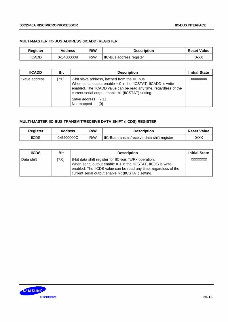
S3C2440A RISC MICROPROCESSOR IIC-BUS INTERFACE
20-13
MULTI-MASTER IIC-BUS ADDRESS (IICADD) REGISTER
Register Address R/W Description Reset Value
IICADD 0x54000008 R/W IIC-Bus address register 0xXX
IICADD Bit Description Initial State
Slave address [7:0] 7-bit slave address, latched from the IIC-bus.When serial output enable = 0 in the IICSTAT, IICADD is write-enabled. The IICADD value can be read any time, regardless of thecurrent serial output enable bit (IICSTAT) setting.
Slave address : [7:1]Not mapped : [0]
XXXXXXXX
MULTI-MASTER IIC-BUS TRANSMIT/RECEIVE DATA SHIFT (IICDS) REGISTER
Register Address R/W Description Reset Value
IICDS 0x5400000C R/W IIC-Bus transmit/receive data shift register 0xXX
IICDS Bit Description Initial State
Data shift [7:0] 8-bit data shift register for IIC-bus Tx/Rx operation.When serial output enable = 1 in the IICSTAT, IICDS is write-enabled. The IICDS value can be read any time, regardless of thecurrent serial output enable bit (IICSTAT) setting.
XXXXXXXX
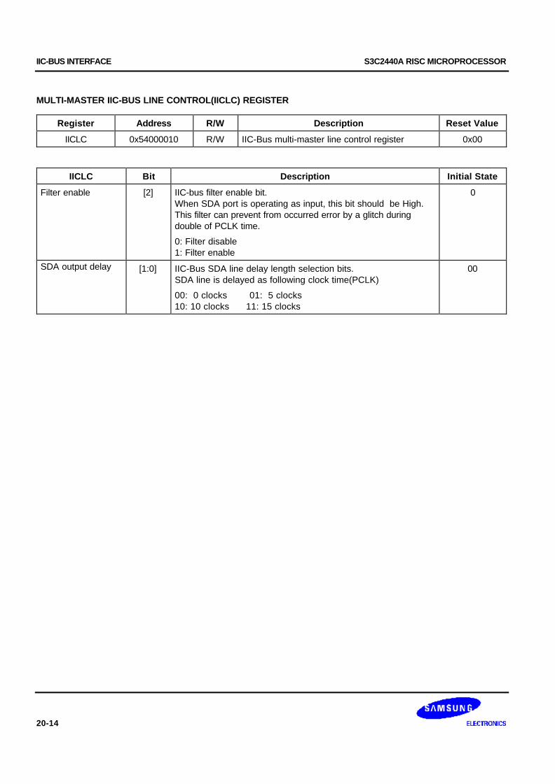
IIC-BUS INTERFACE S3C2440A RISC MICROPROCESSOR
20-14
MULTI-MASTER IIC-BUS LINE CONTROL(IICLC) REGISTER
Register Address R/W Description Reset Value
IICLC 0x54000010 R/W IIC-Bus multi-master line control register 0x00
IICLC Bit Description Initial State
Filter enable [2] IIC-bus filter enable bit.When SDA port is operating as input, this bit should be High.This filter can prevent from occurred error by a glitch duringdouble of PCLK time.
0: Filter disable1: Filter enable
0
SDA output delay [1:0] IIC-Bus SDA line delay length selection bits.SDA line is delayed as following clock time(PCLK)
00: 0 clocks 01: 5 clocks10: 10 clocks 11: 15 clocks
00
S3C2440A RISC MICROPROCESSOR IIS-BUS INTERFACE
21-1
21 IIS-BUS INTERFACE
OVERVIEW
Currently, many digital audio systems are attracting the consumers on the market, in the form of compact discs,digital audio tapes, digital sound processors, and digital TV sound. The S3C2440A Inter-IC Sound (IIS) bus interfacecan be used to implement a CODEC interface to an external 8/16-bit stereo audio CODEC IC for mini-disc andportable applications. The IIS bus interface supports both IIS bus data format and MSB-justified data format. Theinterface provides DMA transfer mode for FIFO access instead of an interrupt. It can transmit and receive datasimultaneously as well as transmit or receive data alternatively at a time.
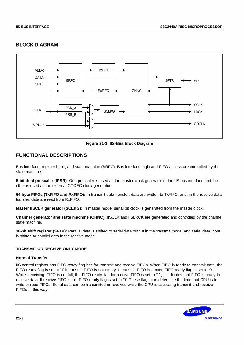
IIS-BUS INTERFACE S3C2440A RISC MICROPROCESSOR
21-2
BLOCK DIAGRAM
ADDR
DATA
CNTL
PCLK
BRFC
IPSR_A
IPSR_B
TxFIFO
RxFIFO
SCLKG
CHNC
SFTR
LRCK
SCLK
SD
CDCLKMPLLin
Figure 21-1. IIS-Bus Block Diagram
FUNCTIONAL DESCRIPTIONS
Bus interface, register bank, and state machine (BRFC): Bus interface logic and FIFO access are controlled by thestate machine.
5-bit dual prescaler (IPSR): One prescaler is used as the master clock generator of the IIS bus interface and theother is used as the external CODEC clock generator.
64-byte FIFOs (TxFIFO and RxFIFO): In transmit data transfer, data are written to TxFIFO, and, in the receive datatransfer, data are read from RxFIFO.
Master IISCLK generator (SCLKG): In master mode, serial bit clock is generated from the master clock.
Channel generator and state machine (CHNC): IISCLK and IISLRCK are generated and controlled by the channelstate machine.
16-bit shift register (SFTR): Parallel data is shifted to serial data output in the transmit mode, and serial data inputis shifted to parallel data in the receive mode.
TRANSMIT OR RECEIVE ONLY MODE
Normal Transfer
IIS control register has FIFO ready flag bits for transmit and receive FIFOs. When FIFO is ready to transmit data, theFIFO ready flag is set to '1' if transmit FIFO is not empty. If transmit FIFO is empty, FIFO ready flag is set to '0'.While receiving FIFO is not full, the FIFO ready flag for receive FIFO is set to '1' ; it indicates that FIFO is ready toreceive data. If receive FIFO is full, FIFO ready flag is set to '0'. These flags can determine the time that CPU is towrite or read FIFOs. Serial data can be transmitted or received while the CPU is accessing transmit and receiveFIFOs in this way.
S3C2440A RISC MICROPROCESSOR IIS-BUS INTERFACE
21-3
DMA TRANSFER
In this mode, transmit or receive FIFO is accessible by the DMA controller. DMA service request in transmit orreceive mode is made by the FIFO ready flag automatically.
TRANSMIT AND RECEIVE MODE
In this mode, IIS bus interface can transmit and receive data simultaneously.
AUDIO SERIAL INTERFACE FORMAT
IIS-BUS FORMAT
The IIS bus has four lines including serial data input (IISDI), serial data output (IISDO), left/right channel select(IISLRCK), and serial bit clock (IISCLK); the device generating IISLRCK and IISCLK is the master.
Serial data is transmitted in 2's complement with the MSB first. The MSB is transmitted first because the transmitterand receiver may have different word lengths. The transmitter does not have to know how many bits the receiver canhandle, nor does the receiver need to know how many bits are being transmitted.
When the system word length is greater than the transmitter word length, the word is truncated (least significant databits are set to '0') for data transmission. If the receiver gets more bits than its word length, the bits after the LSB areignored. On the other hand, if the receiver gets fewer bits than its word length, the missing bits are set to zerointernally. And therefore, the MSB has a fixed position, whereas the position of the LSB depends on the word length.The transmitter sends the MSB of the next word at one clock period whenever the IISLRCK is changed.
Serial data sent by the transmitter may be synchronized with either the trailing (HIGH to LOW) or the leading (LOWto HIGH) edge of the clock signal. However, the serial data must be latched into the receiver on the leading edge ofthe serial clock signal, and so there are some restrictions when transmitting data that is synchronized with theleading edge.
The LR channel select line indicates the channel being transmitted. IISLRCK may be changed either on a trailing orleading edge of the serial clock, but it does not need to be symmetrical. In the slave, this signal is latched on theleading edge of the clock signal. The IISLRCK line changes one clock period before the MSB is transmitted. Thisallows the slave transmitter to derive synchronous timing of the serial data that will be set up for transmission.Furthermore, it enables the receiver to store the previous word and clear the input for the next word.
MSB (LEFT) JUSTIFIED
MSB / left justified bus format is the same as IIS bus format architecturally. Only, different from the IIS bus format,the MSB justified format realizes that the transmitter always sends the MSB of the next word whenever the IISLRCKis changed.

IIS-BUS INTERFACE S3C2440A RISC MICROPROCESSOR
21-4
IIS-bus Format (N=8 or 16)
MSB(1st)
2ndBit
N-1thBit
LSB(last)
MSB(1st)
2ndBit
N-1thBit
LSB(last)
MSB(1st)
LRCK
SCLK
SD
LEFT RIGHT LEFT
MSB-justified Format (N=8 or 16)
2ndBit
N-1thBit
LSB(last)
MSB(1st)
2ndBit
N-1thBit
LSB(last)
LRCK
SCLK
SD
LEFT RIGHT
MSB(1st)
Figure 21-2. IIS-Bus and MSB (Left)-justified Data Interface Formats
SAMPLING FREQUENCY AND MASTER CLOCK
Master clock frequency (PCLK or MPLLin) can be selected by sampling frequency as shown in Table 21-1. BecauseMaster clock is made by IIS prescaler, the prescaler value and Master clock type (256 or 384fs) should bedetermined properly. Serial bit clock frequency type (16/32/48fs) can be selected by the serial bit per channel andMaster clock as shown in Table 21-2.
Table 21-1. CODEC clock (CODECLK = 256 or 384fs)
IISLRCK(fs)
8.000kHz
11.025kHz
16.000kHz
22.050kHz
32.000kHz
44.100kHz
48.000kHz
64.000kHz
88.200kHz
96.000kHz
256fs
CODECLK 2.0480 2.8224 4.0960 5.6448 8.1920 11.2896 12.2880 16.3840 22.5792 24.5760
(MHz) 384fs
3.0720 4.2336 6.1440 8.4672 12.2880 16.9344 18.4320 24.5760 33.8688 36.8640
Table 21-2. Usable Serial Bit Clock Frequency (IISCLK = 16 or 32 or 48fs)
Serial bit per channel 8-bit 16-bit
Serial clock frequency (IISCLK)
@CODECLK = 256fs 16fs, 32fs 32fs
@CODECLK = 384fs 16fs, 32fs, 48fs 32fs, 48fs
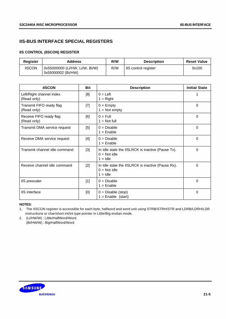
S3C2440A RISC MICROPROCESSOR IIS-BUS INTERFACE
21-5
IIS-BUS INTERFACE SPECIAL REGISTERS
IIS CONTROL (IISCON) REGISTER
Register Address R/W Description Reset Value
IISCON 0x55000000 (Li/HW, Li/W, Bi/W)0x55000002 (Bi/HW)
R/W IIS control register 0x100
IISCON Bit Description Initial State
Left/Right channel index(Read only)
[8] 0 = Left1 = Right
1
Transmit FIFO ready flag(Read only)
[7] 0 = Empty1 = Not empty
0
Receive FIFO ready flag(Read only)
[6] 0 = Full1 = Not full
0
Transmit DMA service request [5] 0 = Disable1 = Enable
0
Receive DMA service request [4] 0 = Disable1 = Enable
0
Transmit channel idle command [3] In Idle state the IISLRCK is inactive (Pause Tx).0 = Not idle1 = Idle
0
Receive channel idle command [2] In Idle state the IISLRCK is inactive (Pause Rx).0 = Not idle1 = Idle
0
IIS prescaler [1] 0 = Disable1 = Enable
0
IIS interface [0] 0 = Disable (stop)1 = Enable (start)
0
NOTES:1. The IISCON register is accessible for each byte, halfword and word unit using STRB/STRH/STR and LDRB/LDRH/LDR instructions or char/short int/int type pointer in Little/Big endian mode.2. (Li/HW/W) : Little/HalfWord/Word
(Bi/HW/W) : Big/HalfWord/Word

IIS-BUS INTERFACE S3C2440A RISC MICROPROCESSOR
21-6
IIS MODE REGISTER (IISMOD) REGISTER
Register Address R/W Description Reset Value
IISMOD 0x55000004 (Li/W, Li/HW, Bi/W)0x55000006 (Bi/HW)
R/W IIS mode register 0x0
IISMOD Bit Description Initial State
Master clock select [9] Master clock select0 = PCLK 1 = MPLLin
0
Master/slave mode select [8] 0 = Master mode (IISLRCK and IISCLK are output mode).1 = Slave mode (IISLRCK and IISCLK are input mode).
0
Transmit/receive modeselect
[7:6] 00 = No transfer 01 = Receive mode10 = Transmit mode 11 = Transmit and receive mode
00
Active level of left/rightchannel
[5] 0 = Low for left channel (High for right channel)1 = High for left channel (Low for right channel)
0
Serial interface format [4] 0 = IIS compatible format1 = MSB (Left)-justified format
0
Serial data bit perchannel
[3] 0 = 8-bit 1 = 16-bit 0
Master clock frequencyselect
[2] 0 = 256fs 1 = 384fs(fs: sampling frequency)
0
Serial bit clock frequencyselect
[1:0] 00 = 16fs 01 = 32fs10 = 48fs 11 = N/A
00
NOTES:1. The IISMOD register is accessible for each halfword and wordunit using STRH/STR and LDRH/LDR instructions orshort int/int type pointer in Little/Big endian mode.2. (Li/HW/W) : Little/HalfWord/Word.
(Bi/HW/W) : Big/HalfWord/Word.

S3C2440A RISC MICROPROCESSOR IIS-BUS INTERFACE
21-7
IIS PRESCALER (IISPSR) REGISTER
Register Address R/W Description Reset Value
IISPSR 0x55000008 (Li/HW, Li/W, Bi/W)0x5500000A (Bi/HW)
R/W IIS prescaler register 0x0
IISPSR Bit Description Initial State
Prescaler control A [9:5] Data value: 0 ~ 31
Note: Prescaler A makes the master clock that is used the internal block and division factor is N+1.
00000
Prescaler control B [4:0] Data value: 0 ~ 31
Note: Prescaler B makes the master clock that is used the external block and division factor is N+1.
00000
NOTES:1. The IISPSR register is accessible for each byte, halfword and word unit using STRB/STRH/STR and LDRB/LDRH/LDR instructions or char/short int/int type pointer in Little/Big endian mode.2. (Li/HW/W): Little/HalfWord/Word.
(Bi/HW/W): Big/HalfWord/Word.

IIS-BUS INTERFACE S3C2440A RISC MICROPROCESSOR
21-8
IIS FIFO CONTROL (IISFCON) REGISTER
Register Address R/W Description Reset Value
IISFCON 0x5500000C (Li/HW, Li/W, Bi/W)0x5500000E (Bi/HW)
R/W IIS FIFO interface register 0x0
IISFCON Bit Description Initial State
Transmit FIFO access mode select [15] 0 = Normal1 = DMA
0
Receive FIFO access mode select [14] 0 = Normal1 = DMA
0
Transmit FIFO [13] 0 = Disable 1 = Enable 0
Receive FIFO [12] 0 = Disable 1 = Enable 0
Transmit FIFO data count(Read only)
[11:6] Data count value = 0 ~ 32 000000
Receive FIFO data count(Read only)
[5:0] Data count value = 0 ~ 32 000000
NOTES:1. The IISFCON register is accessible for each halfword and word unit using STRH/STR and LDRH/LDR instructions or
short int/int type pointer in Little/Big endian mode.2. (Li/HW/W): Little/HalfWord/Word.
(Bi/HW/W): Big/HalfWord/Word.
IIS FIFO (IISFIFO) REGISTER
IIS bus interface contains two 64-byte FIFO for the transmit and receive mode. Each FIFO has 16-width and 32-depthform, which allows the FIFO to handles data for each halfword unit regardless of valid data size. Transmit and receiveFIFO access is performed through FIFO entry; the address of FENTRY is 0x55000010.
Register Address R/W Description Reset Value
IISFIFO 0x55000010(Li/HW)0x55000012(Bi/HW)
R/W IIS FIFO register 0x0
IISFIF Bit Description Initial State
FENTRY [15:0] Transmit/Receive data for IIS 0x0
NOTES:1. The IISFIFO register is accessible for each halfword and word unit using STRH and LDRH instructions or short int type pointer in Little/Big endian mode.2. (Li/HW): Little/HalfWord.
(Bi/HW): Big/HalfWord.
S3C2440A RISC MICROPROCESSOR SPI
22-1
22 SPI
OVERVIEW
The S3C2440A Serial Peripheral Interface (SPI) can interface with the serial data transfer. The S3C2440A includestwo SPI, each of which has two 8-bit shift registers for transmission and receiving, respectively. During an SPItransfer, data is simultaneously transmitted (shifted out serially) and received (shifted in serially). 8-bit serial data ata frequency is determined by its corresponding control register settings. If you only want to transmit, receive datacan be kept dummy. Otherwise, if you only want to receive, you should transmit dummy '1' data.
There are 4 I/O pin signals associated with SPI transfers: SCK (SPICLK0,1), MISO (SPIMISO0,1) data line, MOSI(SPIMOSI0,1) data line and active low /SS (nSS0,1) pin (input).
FEATURES
— Support 2-ch SPI
— SPI Protocol (ver. 2.11) compatible
— 8-bit Shift Register for transmit
— 8-bit Shift Register for receive
— 8-bit Prescaler logic
— Polling, Interrupt and DMA transfer mode
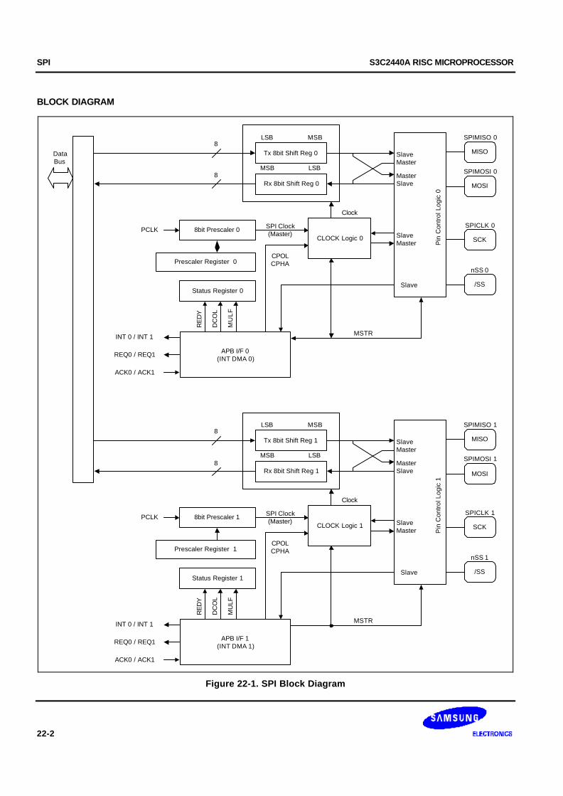
SPI S3C2440A RISC MICROPROCESSOR
22-2
BLOCK DIAGRAM
8bit Prescaler 1PCLK
Status Register 1
Prescaler Register 1
/SS
nSS 0
SCK
SPICLK 0
MOSI
SPIMOSI 0
MISO
SPIMISO 0
Pin
Con
trol
Log
ic 0
MSTR
Tx 8bit Shift Reg 0
Rx 8bit Shift Reg 0
LSB
MSB LSB
MSB8
8
Clock
SPI Clock(Master)
CPOLCPHA
CLOCK Logic 0M
UL
F
DC
OL
RE
DY
APB I/F 0(INT DMA 0)
MasterSlave
SlaveMaster
Slave
SlaveMaster
DataBus
INT 0 / INT 1
REQ0 / REQ1
ACK0 / ACK1
/SS
nSS 1
SCK
SPICLK 1
MOSI
SPIMOSI 1
MISO
SPIMISO 1
Pin
Con
trol
Log
ic 1
MSTR
Tx 8bit Shift Reg 1
Rx 8bit Shift Reg 1
LSB
MSB LSB
MSB8
8
Clock
SPI Clock(Master)
CPOLCPHA
CLOCK Logic 1
MU
LF
DC
OL
RE
DY
APB I/F 1(INT DMA 1)
MasterSlave
SlaveMaster
Slave
SlaveMaster
INT 0 / INT 1
REQ0 / REQ1
ACK0 / ACK1
8bit Prescaler 0PCLK
Status Register 0
Prescaler Register 0
Figure 22-1. SPI Block Diagram

S3C2440A RISC MICROPROCESSOR SPI
22-3
SPI OPERATION
Using the SPI interface, S3C2440A can send/receive 8-bit data simultaneously with an external device. A serialclock line is synchronized with the two data lines for shifting and sampling of the information. When the SPI is themaster, transmission frequency can be controlled by setting the appropriate bit in SPPREn register. You can modifyits frequency to adjust the baud rate data register value. When the SPI is a slave, other master supplies the clock.When the programmer writes byte data to SPTDATn register, SPI transmit/receive operation will startsimultaneously. In some cases, nSS should be activated before writing byte data to SPTDATn.
PROGRAMMING PROCEDURE
When a byte data is written into the SPTDATn register, SPI starts to transmit if ENSCK and MSTR of SPCONnregister are set. You can use a typical programming procedure to operate an SPI card.
To program the SPI modules, follow these basic steps:
1. Set Baud Rate Prescaler Register (SPPREn).
2. Set SPCONn to configure properly the SPI module.
3. Write data 0xFF to SPTDATn 10 times in order to initialize MMC or SD card.
4. Set a GPIO pin, which acts as nSS, low to activate the MMC or SD card.
5. Tx data ¡ Check the status of Transfer Ready flag (REDY=1), and then write data to SPTDATn.
6. Rx data(1): SPCONn's TAGD bit disable = normal mode
7. ¡ write 0xFF to SPTDATn, then confirm REDY to set, and then read data from Read Buffer.
8. Rx data(2): SPCONn's TAGD bit enable = Tx Auto Garbage Data mode
9. ¡ confirm REDY to set, and then read data from Read Buffer (then automatically start to transfer).
10. Set a GPIO pin, which acts as nSS, high to deactivate the MMC or SD card.
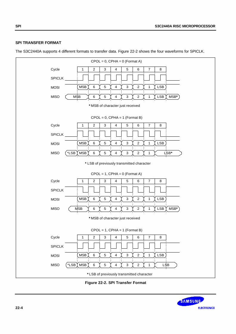
SPI S3C2440A RISC MICROPROCESSOR
22-4
SPI TRANSFER FORMAT
The S3C2440A supports 4 different formats to transfer data. Figure 22-2 shows the four waveforms for SPICLK.
* LSB of previously transmitted character
Cycle
MOSI
1 2 3 4 5 6 7 8
MSB 6 5 4 3 2 1 LSB
6 5 4 3 2 1 LSB
SPICLK
MISO MSB
CPOL = 1, CPHA = 1 (Format B)
* MSB of character just received
Cycle
MOSI
1 2 3 4 5 6 7 8
MSB 6 5 4 3 2 1 LSB
6 5 4 3 2 1 LSB MSB*
SPICLK
MISO MSB
CPOL = 1, CPHA = 0 (Format A)
Cycle
MOSI
1 2 3 4 5 6 7 8
6 5 4 3 2 1 LSB
6 5 4 3 2 1 LSB*
SPICLK
MISO *LSB
CPOL = 0, CPHA = 1 (Format B)
* MSB of character just received
Cycle
MOSI
1 2 3 4 5 6 7 8
MSB 6 5 4 3 2 1 LSB
6 5 4 3 2 1 LSB MSB*
SPICLK
MISO MSB
CPOL = 0, CPHA = 0 (Format A)
* LSB of previously transmitted character
*LSB
MSB
MSB
Figure 22-2. SPI Transfer Format
S3C2440A RISC MICROPROCESSOR SPI
22-5
TRANSMITTING PROCEDURE FOR DMA
1. SPI is configured as DMA mode.
2. DMA is configured properly.
3. SPI requests DMA service.
4. DMA transmits 1byte data to the SPI.
5. SPI transmits the data to card.
6. Return to Step 3 until DMA count becomes 0.
6. SPI is configured as interrupt or polling mode with SMOD bits.
RECEIVING PROCEDURE FOR DMA
1. SPI is configured as DMA start with SMOD bits and TAGD bit set.
2. DMA is configured properly.
3. SPI receives 1byte data from card.
4. SPI requests DMA service.
5. DMA receives the data from the SPI.
6. Write data 0xFF automatically to SPTDATn.
7. Return to Step 4 until DMA count becomes 0.
8. SPI is configured as polling mode with SMOD bits and clear TAGD bit.
9. If SPSTAn’s READY flag is set, then read the last byte data.
NOTE
Total received data = DMA TC values + the last data in polling mode (Step 9).The first DMA received data is dummy and the user can neglect it.
SPI S3C2440A RISC MICROPROCESSOR
22-6
SPI SPECIAL REGISTERS
SPI CONTROL REGISTER
Register Address R/W Description Reset Value
SPCON0 0x59000000 R/W SPI channel 0 control register 0x00
SPCON1 0x59000020 R/W SPI channel 1 control register 0x00
SPCONn Bit Description Initial State
SPI Mode Select(SMOD)
[6:5] Determine how SPTDAT is read/written
00 = polling mode 01 = interrupt mode10 = DMA mode 11 = reserved
00
SCK Enable
(ENSCK)
[4] Determine whether you want SCK enabled or not (master only).
0 = disable 1 = enable
0
Master/SlaveSelect (MSTR)
[3] Determine the desired mode (master or slave).
0 = slave 1 = master
Note: In slave mode, there should be set up time for master to initiateTx/Rx.
0
Clock PolaritySelect (CPOL)
[2] Determine an active high or active low clock.
0 = active high 1 = active low
0
Clock PhaseSelect (CPHA)
[1] Select one of the two fundamentally different transfer format
0 = format A 1 = format B
0
Tx Auto GarbageData modeenable (TAGD)
[0] Decide whether the receiving data is required or not.
0 = normal mode 1 = Tx auto garbage data mode
Note: In normal mode, if you only want to receive data, you shouldtransmit dummy 0xFF data.
0
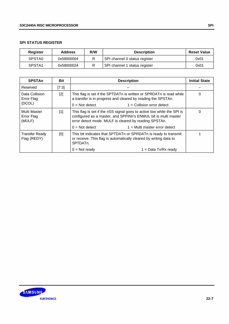
S3C2440A RISC MICROPROCESSOR SPI
22-7
SPI STATUS REGISTER
Register Address R/W Description Reset Value
SPSTA0 0x59000004 R SPI channel 0 status register 0x01
SPSTA1 0x59000024 R SPI channel 1 status register 0x01
SPSTAn Bit Description Initial State
Reserved [7:3] – –
Data CollisionError Flag(DCOL)
[2] This flag is set if the SPTDATn is written or SPRDATn is read whilea transfer is in progress and cleared by reading the SPSTAn.
0 = Not detect 1 = Collision error detect
0
Multi MasterError Flag(MULF)
[1] This flag is set if the nSS signal goes to active low while the SPI isconfigured as a master, and SPPINn's ENMUL bit is multi mastererror detect mode. MULF is cleared by reading SPSTAn.
0 = Not detect 1 = Multi master error detect
0
Transfer ReadyFlag (REDY)
[0] This bit indicates that SPTDATn or SPRDATn is ready to transmitor receive. This flag is automatically cleared by writing data toSPTDATn.
0 = Not ready 1 = Data Tx/Rx ready
1
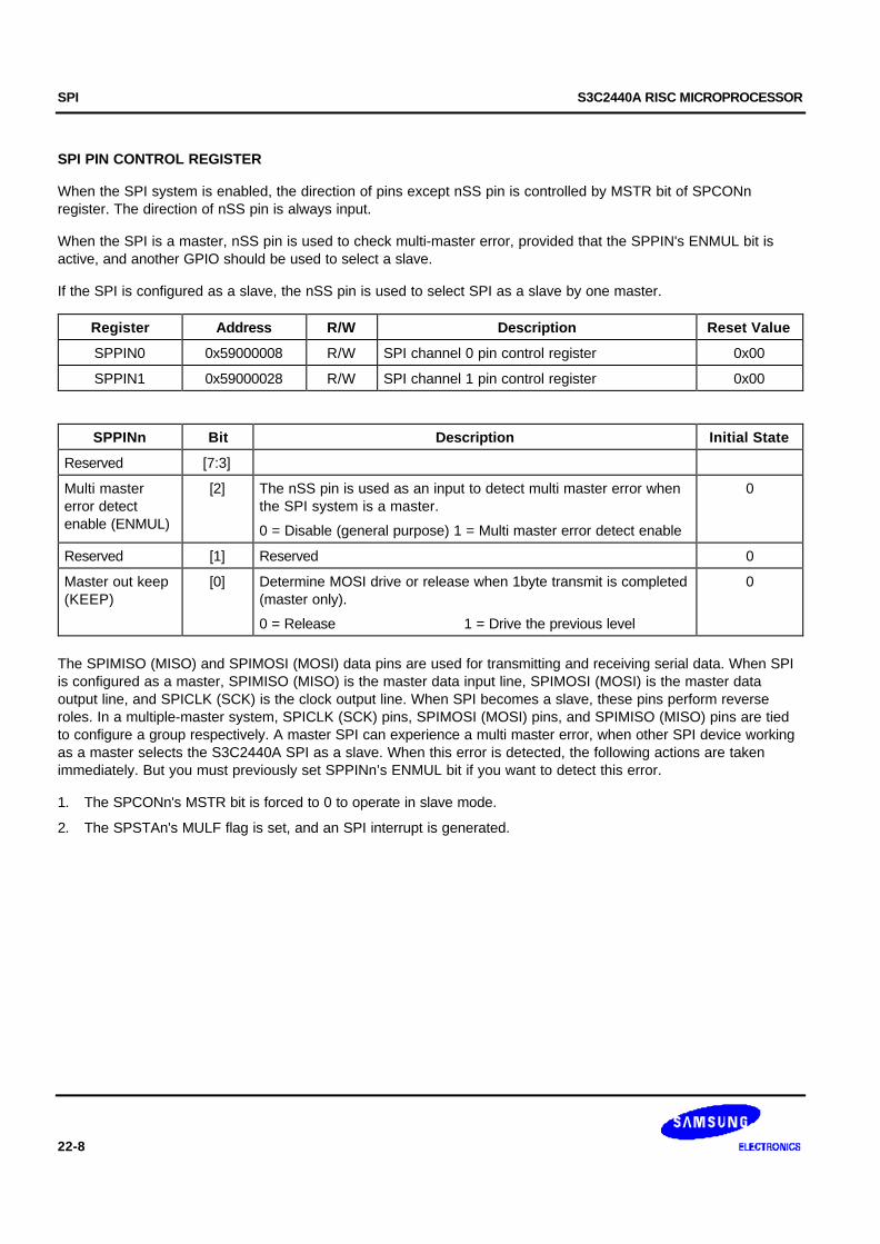
SPI S3C2440A RISC MICROPROCESSOR
22-8
SPI PIN CONTROL REGISTER
When the SPI system is enabled, the direction of pins except nSS pin is controlled by MSTR bit of SPCONnregister. The direction of nSS pin is always input.
When the SPI is a master, nSS pin is used to check multi-master error, provided that the SPPIN's ENMUL bit isactive, and another GPIO should be used to select a slave.
If the SPI is configured as a slave, the nSS pin is used to select SPI as a slave by one master.
Register Address R/W Description Reset Value
SPPIN0 0x59000008 R/W SPI channel 0 pin control register 0x00
SPPIN1 0x59000028 R/W SPI channel 1 pin control register 0x00
SPPINn Bit Description Initial State
Reserved [7:3]
Multi mastererror detectenable (ENMUL)
[2] The nSS pin is used as an input to detect multi master error whenthe SPI system is a master.
0 = Disable (general purpose) 1 = Multi master error detect enable
0
Reserved [1] Reserved 0
Master out keep(KEEP)
[0] Determine MOSI drive or release when 1byte transmit is completed(master only).
0 = Release 1 = Drive the previous level
0
The SPIMISO (MISO) and SPIMOSI (MOSI) data pins are used for transmitting and receiving serial data. When SPIis configured as a master, SPIMISO (MISO) is the master data input line, SPIMOSI (MOSI) is the master dataoutput line, and SPICLK (SCK) is the clock output line. When SPI becomes a slave, these pins perform reverseroles. In a multiple-master system, SPICLK (SCK) pins, SPIMOSI (MOSI) pins, and SPIMISO (MISO) pins are tiedto configure a group respectively. A master SPI can experience a multi master error, when other SPI device workingas a master selects the S3C2440A SPI as a slave. When this error is detected, the following actions are takenimmediately. But you must previously set SPPINn’s ENMUL bit if you want to detect this error.
1. The SPCONn's MSTR bit is forced to 0 to operate in slave mode.
2. The SPSTAn's MULF flag is set, and an SPI interrupt is generated.
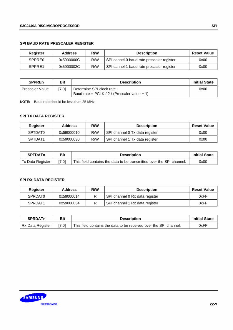
S3C2440A RISC MICROPROCESSOR SPI
22-9
SPI BAUD RATE PRESCALER REGISTER
Register Address R/W Description Reset Value
SPPRE0 0x5900000C R/W SPI cannel 0 baud rate prescaler register 0x00
SPPRE1 0x5900002C R/W SPI cannel 1 baud rate prescaler register 0x00
SPPREn Bit Description Initial State
Prescaler Value [7:0] Determine SPI clock rate.Baud rate = PCLK / 2 / (Prescaler value + 1)
0x00
NOTE: Baud rate should be less than 25 MHz.
SPI TX DATA REGISTER
Register Address R/W Description Reset Value
SPTDAT0 0x59000010 R/W SPI channel 0 Tx data register 0x00
SPTDAT1 0x59000030 R/W SPI channel 1 Tx data register 0x00
SPTDATn Bit Description Initial State
Tx Data Register [7:0] This field contains the data to be transmitted over the SPI channel. 0x00
SPI RX DATA REGISTER
Register Address R/W Description Reset Value
SPRDAT0 0x59000014 R SPI channel 0 Rx data register 0xFF
SPRDAT1 0x59000034 R SPI channel 1 Rx data register 0xFF
SPRDATn Bit Description Initial State
Rx Data Register [7:0] This field contains the data to be received over the SPI channel. 0xFF

SPI S3C2440A RISC MICROPROCESSOR
22-10
NOTES
S3C2440A RISC MICROPROCESSOR CAMERA INTERFACE
23-1
23 CAMERA INTERFACE
OVERVIEW
This chapter will explain the specification and defines the camera interface. CAMIF (CAMera InterFace) within theS3C2440A consists of 7 parts – pattern mux, capturing unit, preview scaler, codec scaler, preview DMA, codecDMA, and SFR. The CAMIF supports ITU-R BT.601/656 YCbCr 8-bit standard. Maximum input size is 4096x4096pixels (2048x2048 pixels for scaling) and two scalers exist. Preview scaler is dedicated to generate smaller sizeimage like PIP (Picture In Picture) and codec scaler is dedicated to generate codec useful image like plane typeYCbCr 4:2:0 or 4:2:2. Two master DMAs can do mirror and rotate the captured image for mobile environments. Thesefeatures are very useful in folder type cellular phones and the test pattern generated can be useful in calibration ofinput sync signals as CAMHREF, CAMVSYNC. Also, video sync signals and pixel clock polarity can be inverted inthe CAMIF side by using register setting.
FEATURES
— ITU-R BT. 601/656 8-bit mode external interface support
— DZI (Digital Zoom In) capability
— Programmable polarity of video sync signals
— Max. 4096 x 4096 pixel input support without scaling (2048 x 2048 pixel input support with scaling)
— Max. 4096 x 4096 pixel output support for CODEC path
— Max. 640 x 480 pixel output support for PREVIEW path
— Image mirror and rotation (X-axis mirror, Y-axis mirror, and 180° rotation)
— PIP and codec input image generation (RGB 16/24-bit format and YCbCr 4:2:0/4:2:2 format)
SIGNAL DESCRIPTION
Table 23-1. Camera Interface Signal Description
Name I/O Active Description
CAMPCLK I – Pixel clock, driven by the camera processor
CAMVSYNC I H/L Frame sync, driven by the camera processor
CAMHREF I H/L Horizontal sync, driven by the camera processor
CAMDATA[7:0] I – Pixel data driven by the camera processor
CAMCLKOUT O – Master clock to the camera processor
CAMRESET O H/L Software reset or power down to the camera processor
NOTE: I/O direction is on the AP side. I: input, O: output
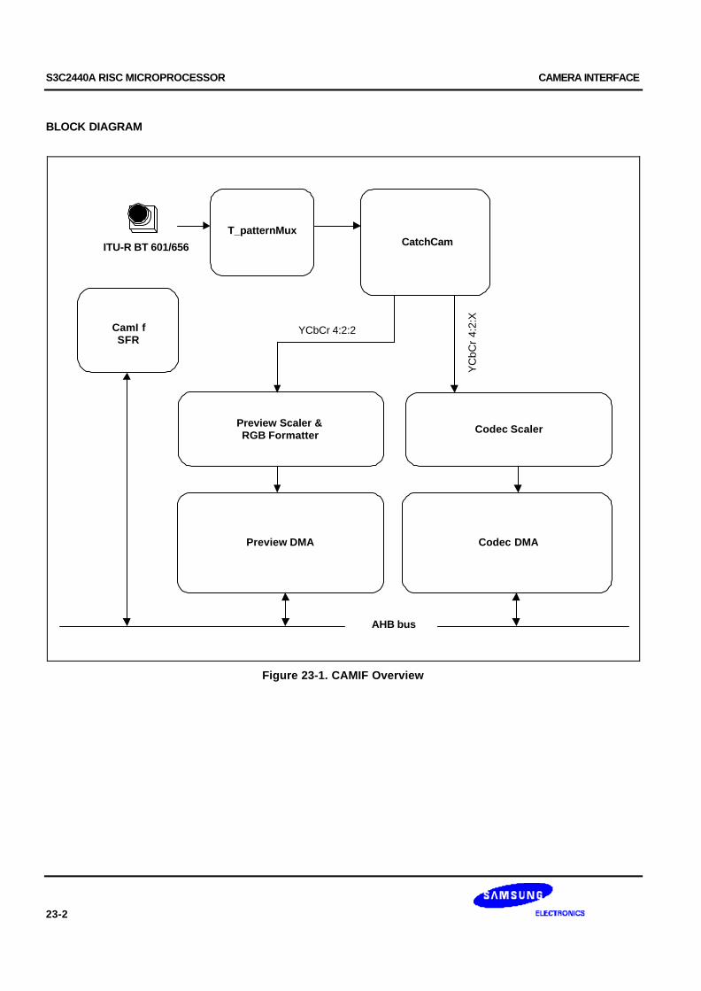
S3C2440A RISC MICROPROCESSOR CAMERA INTERFACE
23-2
BLOCK DIAGRAM
YCbCr 4:2:2
T_patternMuxCatchCam
YC
bCr
4:2:
X
Preview Scaler &RGB Formatter Codec Scaler
Preview DMA
ITU-R BT 601/656
Codec DMA
CamI fSFR
AHB bus
Figure 23-1. CAMIF Overview
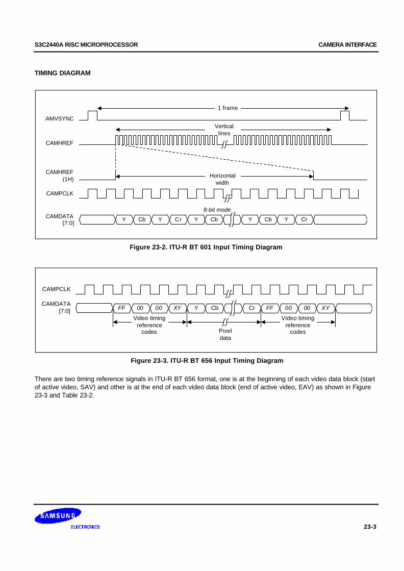
S3C2440A RISC MICROPROCESSOR CAMERA INTERFACE
23-3
TIMING DIAGRAM
CAMVSYNC
Y Cb Y Cr Y Cb Y Cb Y Cr
CAMHREF
CAMHREF(1H)
CAMPCLK
CAMDATA[7:0]
Verticallines
Horizontalwidth
1 frame
8-bit mode
Figure 23-2. ITU-R BT 601 Input Timing Diagram
CAMPCLK
CAMDATA[7:0] CrFF 00 00 XY CbY FF 00 00 XY
Video timingreference
codes Pixeldata
Video timingreference
codes
Figure 23-3. ITU-R BT 656 Input Timing Diagram
There are two timing reference signals in ITU-R BT 656 format, one is at the beginning of each video data block (startof active video, SAV) and other is at the end of each video data block (end of active video, EAV) as shown in Figure23-3 and Table 23-2.
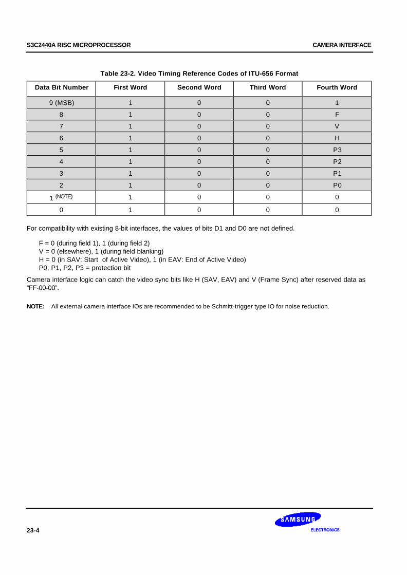
S3C2440A RISC MICROPROCESSOR CAMERA INTERFACE
23-4
Table 23-2. Video Timing Reference Codes of ITU-656 Format
Data Bit Number First Word Second Word Third Word Fourth Word
9 (MSB) 1 0 0 1
8 1 0 0 F
7 1 0 0 V
6 1 0 0 H
5 1 0 0 P3
4 1 0 0 P2
3 1 0 0 P1
2 1 0 0 P0
1 (NOTE) 1 0 0 0
0 1 0 0 0
For compatibility with existing 8-bit interfaces, the values of bits D1 and D0 are not defined.
F = 0 (during field 1), 1 (during field 2)V = 0 (elsewhere), 1 (during field blanking)H = 0 (in SAV: Start of Active Video), 1 (in EAV: End of Active Video)P0, P1, P2, P3 = protection bit
Camera interface logic can catch the video sync bits like H (SAV, EAV) and V (Frame Sync) after reserved data as“FF-00-00”.
NOTE: All external camera interface IOs are recommended to be Schmitt-trigger type IO for noise reduction.
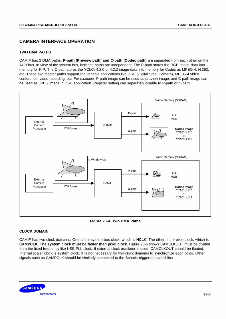
S3C2440A RISC MICROPROCESSOR CAMERA INTERFACE
23-5
CAMERA INTERFACE OPERATION
TWO DMA PATHS
CAMIF has 2 DMA paths. P-path (Preview path) and C-path (Codec path) are separated from each other on theAHB bus. In view of the system bus, both the paths are independent. The P-path stores the RGB image data intomemory for PIP. The C-path stores the YCbCr 4:2:0 or 4:2:2 image data into memory for Codec as MPEG-4, H.263,etc. These two master paths support the variable applications like DSC (Digital Steel Camera), MPEG-4 videoconference, video recording, etc. For example, P-path image can be used as preview image, and C-path image canbe used as JPEG image in DSC application. Register setting can separately disable to P-path or C-path.
CAMIFExternalCamera
Processor
Frame Memory (SDRAM)
P-port
C-portITU format
PIPRGB
Codec imageYCbCr 4:2:0
orYCbCr 4:2:2
Window cut
CAMIFExternalCamera
Processor
Frame Memory (SDRAM)
P-port
C-portITU format
PIPRGB
Codec imageYCbCr 4:2:0
orYCbCr 4:2:2
Figure 23-4. Two DMA Paths
CLOCK DOMAIN
CAMIF has two clock domains. One is the system bus clock, which is HCLK. The other is the pixel clock, which isCAMPCLK. The system clock must be faster than pixel clock. Figure 23-5 shows CAMCLKOUT must be dividedfrom the fixed frequency like USB PLL clock. If external clock oscillator is used, CAMCLKOUT should be floated.Internal scaler clock is system clock. It is not necessary for two clock domains to synchronize each other. Othersignals such as CAMPCLK should be similarly connected to the Schmitt-triggered level shifter.

S3C2440A RISC MICROPROCESSOR CAMERA INTERFACE
23-6
FRAME MEMORY HIRERARCHY
Frame memories consist of four ping-pong memories for each of P and C paths as shown in the Figure 23-6. C-path ping-pong memories have three element memories – luminance Y, chrominance Cb, and chrominance Cr. IfAHB-bus traffic is not enough for the DMA operation to complete during one horizontal line period, it may lead to mal-functioning
CAMCLKOUTDivide
Counter1/1 ~ 1/16
UPLL
ExternalCamera
ProcessorCAMPCLK
S3C2440A
CAMIF
USB PLL96 MHz
fUSB /d
fUSB
MPLL VariableFreq.
DivideCounter
fmpll /d
fmpll
HCLK
a External MCLK
Normally use
Schmit-triggered
Level-shifter
Figure 23-5. CAMIF Clock Generation

S3C2440A RISC MICROPROCESSOR CAMERA INTERFACE
23-7
C-port Y 1
C-port Cb 1
C-port Cr 1
C-port Y 2
C-port Cb 2
C-port Cr 2
C-port Y 3
C-port Cb 3C-port Cr 3
C-port Y 4
C-port Cb 4
C-port Cr 4
P-port RGB 1
P-port RGB 2
P-port RGB 3
P-port RGB 4
4-PingpongFrame Memory (SDRAM)
ITU-601/656YCbCr4:2:28-bits
Camera Interface AHB bus &Memorycontroller
P-portRGB4:4:4
C-port4:2:0,2
Figure 23-6. Ping-Pong Memory Hierarchy
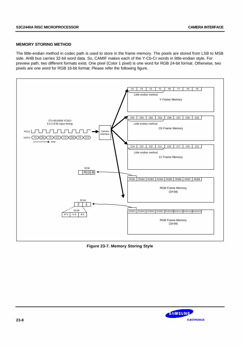
S3C2440A RISC MICROPROCESSOR CAMERA INTERFACE
23-8
MEMORY STORING METHOD
The little-endian method in codec path is used to store in the frame memory. The pixels are stored from LSB to MSBside. AHB bus carries 32-bit word data. So, CAMIF makes each of the Y-Cb-Cr words in little-endian style. Forpreview path, two different formats exist. One pixel (Color 1 pixel) is one word for RGB 24-bit format. Otherwise, twopixels are one word for RGB 16-bit format. Please refer the following figure.
CameraInterface
Y Frame Memory
PCLK
DATA
ITU-601/656 YCbCr4:2:2 8-bit input timing
Cb Frame Memory
Cr Frame Memory
Little endian method
time
Y1 Cb1 Y2 Cr1 Y3 Cb2 Y4 Cr2
Y4 Y3 Y2 Y1 Y8 Y7 Y6 Y5
Cb4 Cb3 Cb2 Cb1 Cb8 Cb7 Cb6 Cb5
Little endian method
Cr4 Cr3 Cr2 Cr1 Cr8 Cr7 Cr6 Cr5
Little endian method
RGB Frame Memory(24-bit)
RGB1 RGB2 RGB3 RGB4 RGB5 RGB6 RGB7 RGB8
RGB Frame Memory(16-bit)
RGB2/1 RGB4/3 RGB6/5 RGB8/7 RGB10/9 RGB12/11 RGB14/13 RGB16/15
32-bit
R G B
232-bit
1
R 5 G 6 B 5
16-bit
Figure 23-7. Memory Storing Style
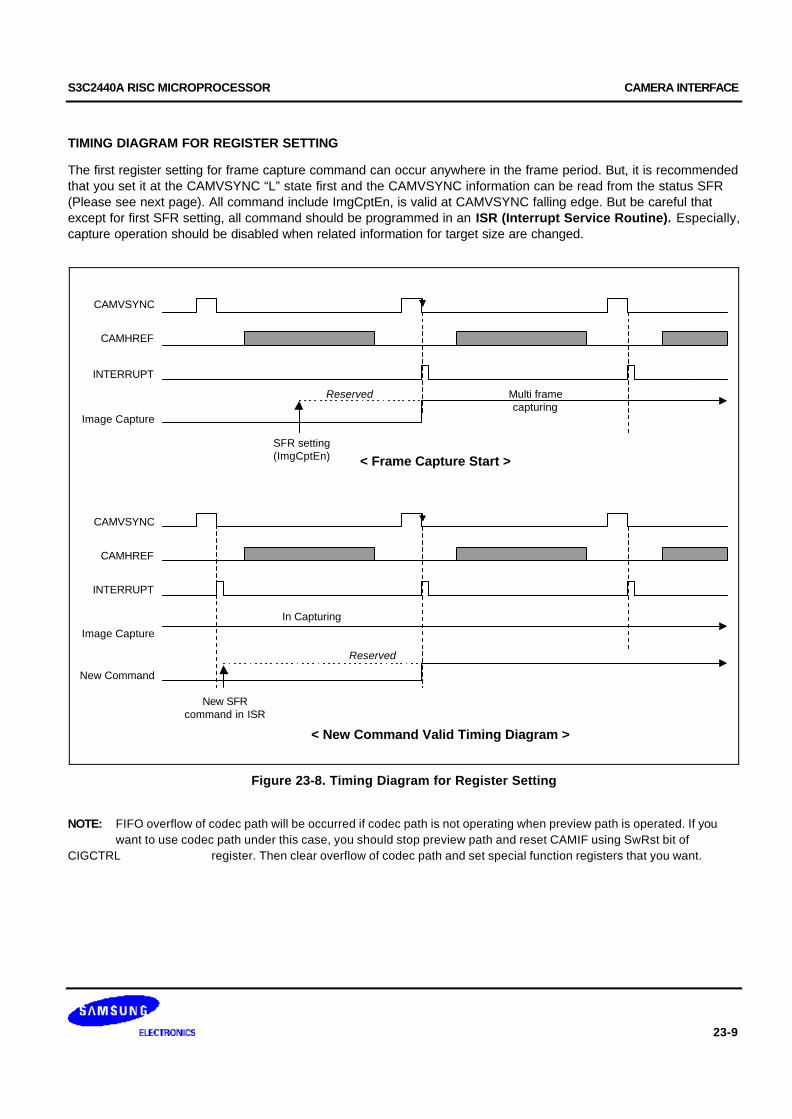
S3C2440A RISC MICROPROCESSOR CAMERA INTERFACE
23-9
TIMING DIAGRAM FOR REGISTER SETTING
The first register setting for frame capture command can occur anywhere in the frame period. But, it is recommendedthat you set it at the CAMVSYNC “L” state first and the CAMVSYNC information can be read from the status SFR(Please see next page). All command include ImgCptEn, is valid at CAMVSYNC falling edge. But be careful thatexcept for first SFR setting, all command should be programmed in an ISR (Interrupt Service Routine). Especially,capture operation should be disabled when related information for target size are changed.
CAMVSYNC
CAMHREF
INTERRUPT
SFR setting(ImgCptEn)
Multi framecapturing
Reserved
Image Capture
< Frame Capture Start >
CAMVSYNC
CAMHREF
INTERRUPT
New SFRcommand in ISR
In Capturing
Reserved
Image Capture
< New Command Valid Timing Diagram >
New Command
Figure 23-8. Timing Diagram for Register Setting
NOTE: FIFO overflow of codec path will be occurred if codec path is not operating when preview path is operated. If you want to use codec path under this case, you should stop preview path and reset CAMIF using SwRst bit ofCIGCTRL register. Then clear overflow of codec path and set special function registers that you want.
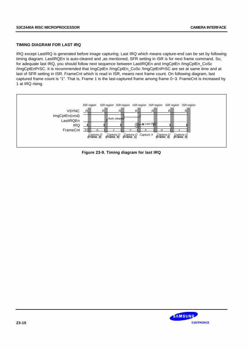
S3C2440A RISC MICROPROCESSOR CAMERA INTERFACE
23-10
TIMING DIAGRAM FOR LAST IRQ
IRQ except LastIRQ is generated before image capturing. Last IRQ which means capture-end can be set by followingtiming diagram. LastIRQEn is auto-cleared and ,as mentioned, SFR setting in ISR is for next frame command. So,for adequate last IRQ, you should follow next sequence between LastIRQEn and ImgCptEn /ImgCptEn_CoSc/ImgCptEnPrSC. It is recommended that ImgCptEn /ImgCptEn_CoSc /ImgCptEnPrSC are set at same time and atlast of SFR setting in ISR. FrameCnt which is read in ISR, means next frame count. On following diagram, lastcaptured frame count is “1”. That is, Frame 1 is the last-captured frame among frame 0~3. FrameCnt is increased by1 at IRQ rising.
ISR regionISR regionISR region
VSYNC
ISR region
ImgCptEn(cmd)LastIRQEn
Capture O Capture O Capture O Capture X
IRQ
Auto cleared
Last IRQ
ISR region ISR region ISR region
FrameCntCapture O Capture O
(Frame_3) (Frame_0) (Frame_1) (Frame_3) (Frame_0)
0 1 2 33 0 1
Figure 23-9. Timing diagram for last IRQ
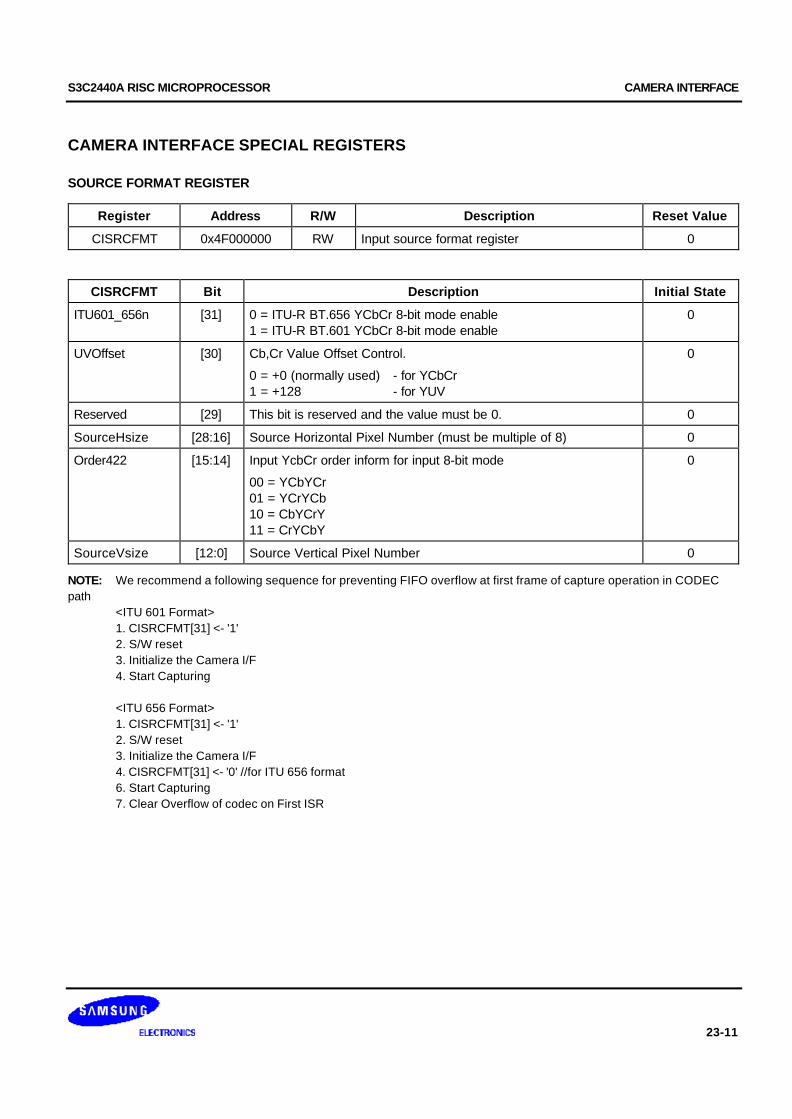
S3C2440A RISC MICROPROCESSOR CAMERA INTERFACE
23-11
CAMERA INTERFACE SPECIAL REGISTERS
SOURCE FORMAT REGISTER
Register Address R/W Description Reset Value
CISRCFMT 0x4F000000 RW Input source format register 0
CISRCFMT Bit Description Initial State
ITU601_656n [31] 0 = ITU-R BT.656 YCbCr 8-bit mode enable1 = ITU-R BT.601 YCbCr 8-bit mode enable
0
UVOffset [30] Cb,Cr Value Offset Control.
0 = +0 (normally used) - for YCbCr1 = +128 - for YUV
0
Reserved [29] This bit is reserved and the value must be 0. 0
SourceHsize [28:16] Source Horizontal Pixel Number (must be multiple of 8) 0
Order422 [15:14] Input YcbCr order inform for input 8-bit mode
00 = YCbYCr01 = YCrYCb10 = CbYCrY11 = CrYCbY
0
SourceVsize [12:0] Source Vertical Pixel Number 0
NOTE: We recommend a following sequence for preventing FIFO overflow at first frame of capture operation in CODECpath
<ITU 601 Format>1. CISRCFMT[31] <- '1'2. S/W reset3. Initialize the Camera I/F4. Start Capturing
<ITU 656 Format>1. CISRCFMT[31] <- '1'2. S/W reset3. Initialize the Camera I/F4. CISRCFMT[31] <- '0' //for ITU 656 format6. Start Capturing7. Clear Overflow of codec on First ISR
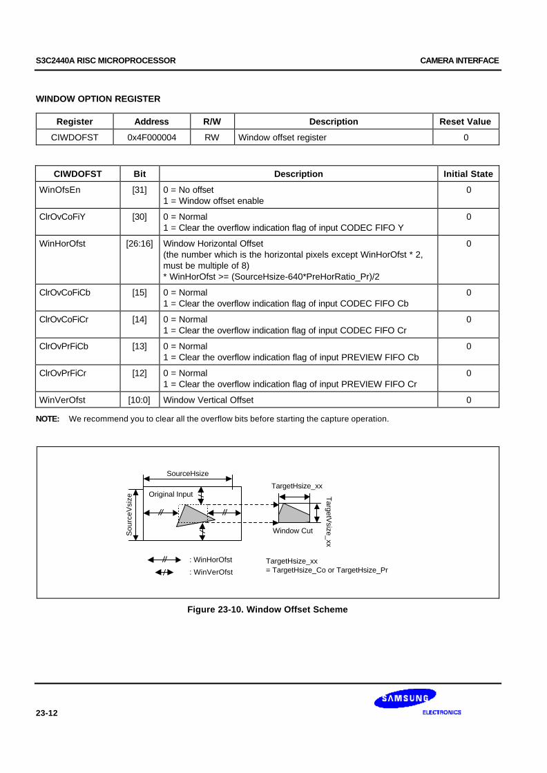
S3C2440A RISC MICROPROCESSOR CAMERA INTERFACE
23-12
WINDOW OPTION REGISTER
Register Address R/W Description Reset Value
CIWDOFST 0x4F000004 RW Window offset register 0
CIWDOFST Bit Description Initial State
WinOfsEn [31] 0 = No offset1 = Window offset enable
0
ClrOvCoFiY [30] 0 = Normal1 = Clear the overflow indication flag of input CODEC FIFO Y
0
WinHorOfst [26:16] Window Horizontal Offset(the number which is the horizontal pixels except WinHorOfst * 2,must be multiple of 8)* WinHorOfst >= (SourceHsize-640*PreHorRatio_Pr)/2
0
ClrOvCoFiCb [15] 0 = Normal1 = Clear the overflow indication flag of input CODEC FIFO Cb
0
ClrOvCoFiCr [14] 0 = Normal1 = Clear the overflow indication flag of input CODEC FIFO Cr
0
ClrOvPrFiCb [13] 0 = Normal1 = Clear the overflow indication flag of input PREVIEW FIFO Cb
0
ClrOvPrFiCr [12] 0 = Normal1 = Clear the overflow indication flag of input PREVIEW FIFO Cr
0
WinVerOfst [10:0] Window Vertical Offset 0
NOTE: We recommend you to clear all the overflow bits before starting the capture operation.
SourceHsize
Sou
rceV
size
Original Input
Window Cut
: WinHorOfst
: WinVerOfst
TargetHsize_xx
TargetHsize_xx= TargetHsize_Co or TargetHsize_Pr
TargetV
size_xx
Figure 23-10. Window Offset Scheme
S3C2440A RISC MICROPROCESSOR CAMERA INTERFACE
23-13
GLOBAL CONTROL REGISTER
Register Address R/W Description Reset Value
CIGCTRL 0x4F000008 RW Global control register 0
CIGCTRL Bit Description Initial State
SwRst [31] Camera interface software reset 0
CamRst [30] External camera processor reset or power down 0
Reserved [29] This bit is reserved and the value must be 1. 1
TestPattern [28:27] This register should be set only at ITU-T 601 8-bit mode. It is notallowed with ITU-T 656 mode. (max. 1280 X 1024)
00 = External camera processor input (normal)01 = Color bar test pattern10 = Horizontal increment test pattern11 = Vertical increment test pattern
0
InvPolCAMPCLK [26] 0 = Normal1 = Inverse the polarity of CAMPCLK
0
InvPolCAMVSYNC [25] 0 = Normal1 = Inverse the polarity of CAMVSYNC
0
InvPolCAMHREF [24] 0 = Normal1 = Inverse the polarity of CAMHREF
0
Y1 START ADDRESS REGISTER
Register Address R/W Description Reset Value
CICOYSA1 0x4F000018 RW Y 1st frame start address for codec DMA 0
CICOYSA1 Bit Description Initial State
CICOYSA1 [31:0] Y 1st frame start address for codec DMA 0
NOTE: Address of buffers must be multiple of 1024.
Y2 START ADDRESS REGISTER
Register Address R/W Description Reset Value
CICOYSA2 0x4F00001C RW Y 2nd frame start address for codec DMA 0
CICOYSA2 Bit Description Initial State
CICOYSA2 [31:0] Y 2nd frame start address for codec DMA 0
S3C2440A RISC MICROPROCESSOR CAMERA INTERFACE
23-14
Y3 START ADDRESS REGISTER
Register Address R/W Description Reset Value
CICOYSA3 0x4F000020 RW Y 3nd frame start address for codec DMA 0
CICOYSA3 Bit Description Initial State
CICOYSA3 [31:0] Y 3nd frame start address for codec DMA 0
Y4 START ADDRESS REGISTER
Register Address R/W Description Reset Value
CICOYSA4 0x4F000024 RW Y 4th frame start address for codec DMA 0
CICOYSA4 Bit Description Initial State
CICOYSA4 [31:0] Y 4th frame start address for codec DMA 0
CB1 START ADDRESS REGISTER
Register Address R/W Description Reset Value
CICOCBSA1 0x4F000028 RW Cb 1st frame start address for codec DMA 0
CICOCBSA1 Bit Description Initial State
CICOCBSA1 [31:0] Cb 1st frame start address for codec DMA 0
CB2 START ADDRESS REGISTER
Register Address R/W Description Reset Value
CICOCBSA2 0x4F00002C RW Cb 2nd frame start address for codec DMA 0
CICOCBSA2 Bit Description Initial State
CICOCBSA2 [31:0] Cb 2nd frame start address for codec DMA 0
S3C2440A RISC MICROPROCESSOR CAMERA INTERFACE
23-15
CB3 START ADDRESS REGISTER
Register Address R/W Description Reset Value
CICOCBSA3 0x4F000030 RW Cb 3nd frame start address for codec DMA 0
CICOCBSA3 Bit Description Initial State
CICOCBSA3 [31:0] Cb 3nd frame start address for codec DMA 0
CB4 START ADDRESS REGISTER
Register Address R/W Description Reset Value
CICOCBSA4 0x4F000034 RW Cb 4th frame start address for codec DMA 0
CICOCBSA4 Bit Description Initial State
CICOCBSA4 [31:0] Cb 4th frame start address for codec DMA 0
CR1 START ADDRESS REGISTER
Register Address R/W Description Reset Value
CICOCRSA1 0x4F000038 RW Cr 1st frame start address for codec DMA 0
CICOCRSA1 Bit Description Initial State
CICOCRSA1 [31:0] Cr 1st frame start address for codec DMA 0
CR2 START ADDRESS REGISTER
Register Address R/W Description Reset Value
CICOCRSA2 0x4F00003C RW Cr 2nd frame start address for codec DMA 0
CICOCRSA2 Bit Description Initial State
CICOCRSA2 [31:0] Cr 2nd frame start address for codec DMA 0

S3C2440A RISC MICROPROCESSOR CAMERA INTERFACE
23-16
CR3 START ADDRESS REGISTER
Register Address R/W Description Reset Value
CICOCRSA3 0x4F000040 RW Cr 3nd frame start address for codec DMA 0
CICOCRSA3 Bit Description Initial State
CICOCRSA3 [31:0] Cr 3nd frame start address for codec DMA 0
CR4 START ADDRESS REGISTER
Register Address R/W Description Reset Value
CICOCRSA4 0x4F000044 RW Cr 4th frame start address for codec DMA 0
CICOCRSA4 Bit Description Initial State
CICOCRSA4 [31:0] Cr 4th frame start address for codec DMA 0
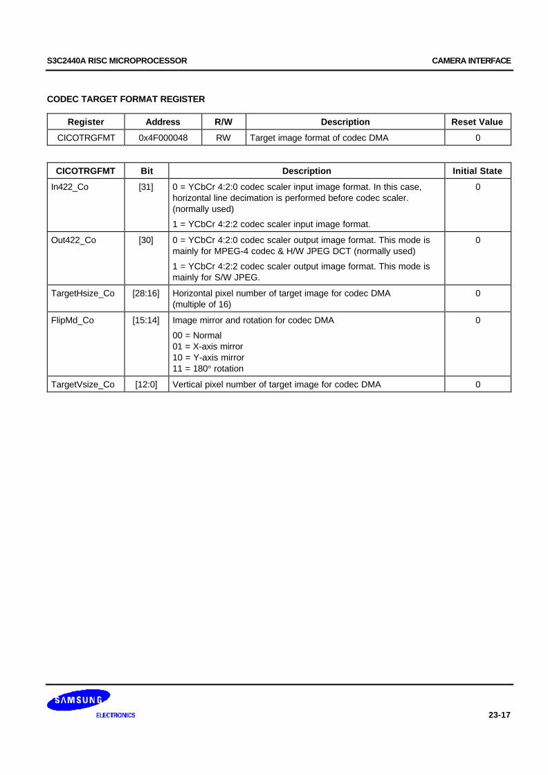
S3C2440A RISC MICROPROCESSOR CAMERA INTERFACE
23-17
CODEC TARGET FORMAT REGISTER
Register Address R/W Description Reset Value
CICOTRGFMT 0x4F000048 RW Target image format of codec DMA 0
CICOTRGFMT Bit Description Initial State
In422_Co [31] 0 = YCbCr 4:2:0 codec scaler input image format. In this case,horizontal line decimation is performed before codec scaler.(normally used)
1 = YCbCr 4:2:2 codec scaler input image format.
0
Out422_Co [30] 0 = YCbCr 4:2:0 codec scaler output image format. This mode ismainly for MPEG-4 codec & H/W JPEG DCT (normally used)
1 = YCbCr 4:2:2 codec scaler output image format. This mode ismainly for S/W JPEG.
0
TargetHsize_Co [28:16] Horizontal pixel number of target image for codec DMA(multiple of 16)
0
FlipMd_Co [15:14] Image mirror and rotation for codec DMA
00 = Normal01 = X-axis mirror10 = Y-axis mirror11 = 180° rotation
0
TargetVsize_Co [12:0] Vertical pixel number of target image for codec DMA 0

S3C2440A RISC MICROPROCESSOR CAMERA INTERFACE
23-18
Original Image
X-Axis Flip
Y-Axis Flip
180° Rotation
Figure 23-11. Image Mirror and Rotation
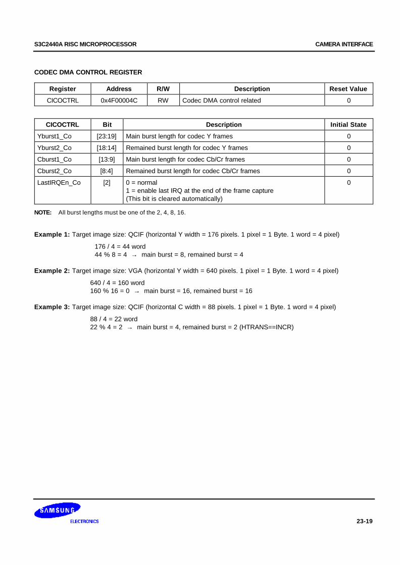
S3C2440A RISC MICROPROCESSOR CAMERA INTERFACE
23-19
CODEC DMA CONTROL REGISTER
Register Address R/W Description Reset Value
CICOCTRL 0x4F00004C RW Codec DMA control related 0
CICOCTRL Bit Description Initial State
Yburst1_Co [23:19] Main burst length for codec Y frames 0
Yburst2_Co [18:14] Remained burst length for codec Y frames 0
Cburst1_Co [13:9] Main burst length for codec Cb/Cr frames 0
Cburst2_Co [8:4] Remained burst length for codec Cb/Cr frames 0
LastIRQEn_Co [2] 0 = normal1 = enable last IRQ at the end of the frame capture(This bit is cleared automatically)
0
NOTE: All burst lengths must be one of the 2, 4, 8, 16.
Example 1: Target image size: QCIF (horizontal Y width = 176 pixels. 1 pixel = 1 Byte. 1 word = 4 pixel)
176 / 4 = 44 word 44 % 8 = 4 → main burst = 8, remained burst = 4
Example 2: Target image size: VGA (horizontal Y width = 640 pixels. 1 pixel = 1 Byte. 1 word = 4 pixel)
640 / 4 = 160 word160 % 16 = 0 → main burst = 16, remained burst = 16
Example 3: Target image size: QCIF (horizontal C width = 88 pixels. 1 pixel = 1 Byte. 1 word = 4 pixel)
88 / 4 = 22 word22 % 4 = 2 → main burst = 4, remained burst = 2 (HTRANS==INCR)
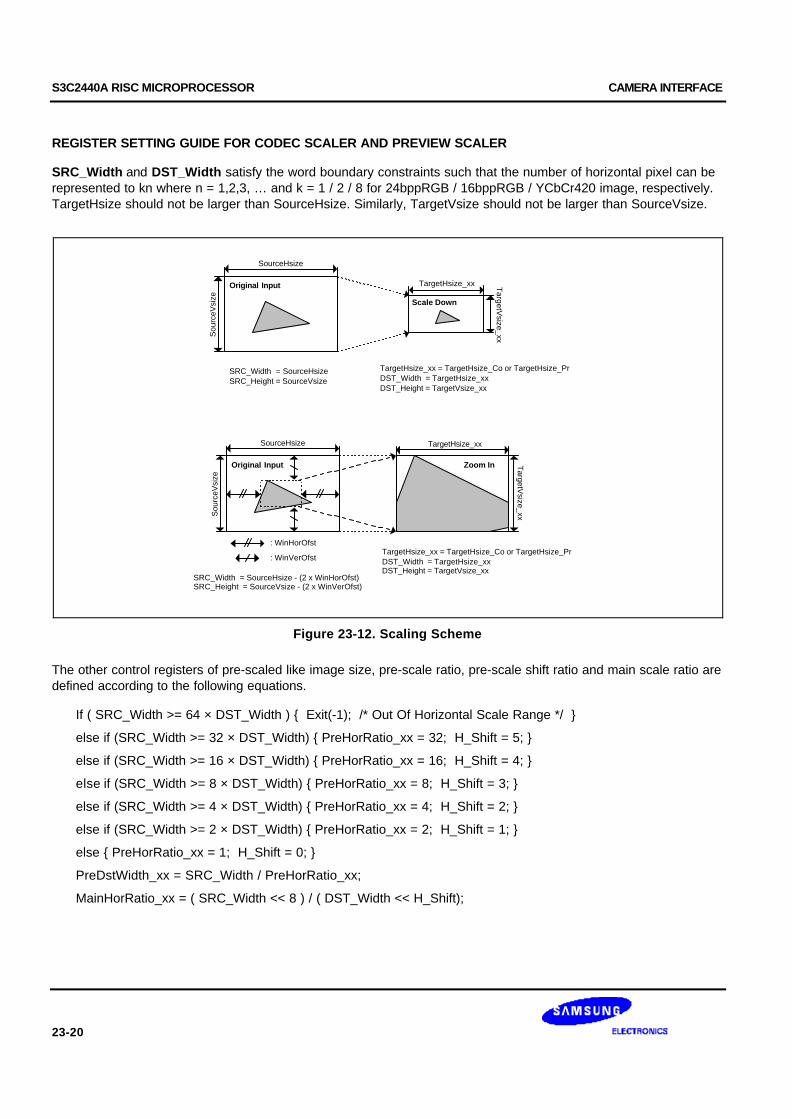
S3C2440A RISC MICROPROCESSOR CAMERA INTERFACE
23-20
REGISTER SETTING GUIDE FOR CODEC SCALER AND PREVIEW SCALER
SRC_Width and DST_Width satisfy the word boundary constraints such that the number of horizontal pixel can berepresented to kn where n = 1,2,3, … and k = 1 / 2 / 8 for 24bppRGB / 16bppRGB / YCbCr420 image, respectively.TargetHsize should not be larger than SourceHsize. Similarly, TargetVsize should not be larger than SourceVsize.
SourceHsize
Sou
rceV
size
TargetHsize_xx TargetV
size_xxOriginal Input
Scale Down
SourceHsize
Sou
rceV
size
Original Input Zoom In
: WinHorOfst
: WinVerOfst
TargetHsize_xx
TargetV
size_xx
SRC_Width = SourceHsizeSRC_Height = SourceVsize
TargetHsize_xx = TargetHsize_Co or TargetHsize_PrDST_Width = TargetHsize_xxDST_Height = TargetVsize_xx
TargetHsize_xx = TargetHsize_Co or TargetHsize_PrDST_Width = TargetHsize_xxDST_Height = TargetVsize_xx
SRC_Width = SourceHsize - (2 x WinHorOfst)SRC_Height = SourceVsize - (2 x WinVerOfst)
Figure 23-12. Scaling Scheme
The other control registers of pre-scaled like image size, pre-scale ratio, pre-scale shift ratio and main scale ratio aredefined according to the following equations.
If ( SRC_Width >= 64 × DST_Width ) Exit(-1); /* Out Of Horizontal Scale Range */
else if (SRC_Width >= 32 × DST_Width) PreHorRatio_xx = 32; H_Shift = 5;
else if (SRC_Width >= 16 × DST_Width) PreHorRatio_xx = 16; H_Shift = 4;
else if (SRC_Width >= 8 × DST_Width) PreHorRatio_xx = 8; H_Shift = 3;
else if (SRC_Width >= 4 × DST_Width) PreHorRatio_xx = 4; H_Shift = 2;
else if (SRC_Width >= 2 × DST_Width) PreHorRatio_xx = 2; H_Shift = 1;
else PreHorRatio_xx = 1; H_Shift = 0;
PreDstWidth_xx = SRC_Width / PreHorRatio_xx;
MainHorRatio_xx = ( SRC_Width << 8 ) / ( DST_Width << H_Shift);
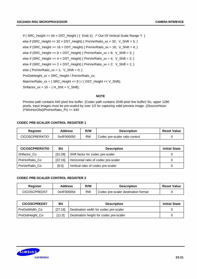
S3C2440A RISC MICROPROCESSOR CAMERA INTERFACE
23-21
If ( SRC_Height >= 64 × DST_Height ) Exit(-1); /* Out Of Vertical Scale Range */
else if (SRC_Height >= 32 × DST_Height) PreVerRatio_xx = 32; V_Shift = 5;
else if (SRC_Height >= 16 × DST_Height) PreVerRatio_xx = 16; V_Shift = 4;
else if (SRC_Height >= 8 × DST_Height) PreVerRatio_xx = 8; V_Shift = 3;
else if (SRC_Height >= 4 × DST_Height) PreVerRatio_xx = 4; V_Shift = 2;
else if (SRC_Height >= 2 × DST_Height) PreVerRatio_xx = 2; V_Shift = 1;
else PreVerRatio_xx = 1; V_Shift = 0;
PreDstHeight_xx = SRC_Height / PreVerRatio_xx;
MainVerRatio_xx = ( SRC_Height << 8 ) / ( DST_Height << V_Shift);
SHfactor_xx = 10 – ( H_Shit + V_Shift);
NOTE
Preview path contains 640 pixel line buffer. (Codec path contains 2048 pixel line buffer) So, upper 1280pixels, input images must be pre-scaled by over 1/2 for capturing valid preview image. ((SourceHsize-2*WinHorOfst)/PreHorRatio_Pr) <= 640
CODEC PRE-SCALER CONTROL REGISTER 1
Register Address R/W Description Reset Value
CICOSCPRERATIO 0x4F000050 RW Codec pre-scaler ratio control 0
CICOSCPRERATIO Bit Description Initial State
SHfactor_Co [31:28] Shift factor for codec pre-scaler 0
PreHorRatio_Co [22:16] Horizontal ratio of codec pre-scaler 0
PreVerRatio_Co [6:0] Vertical ratio of codec pre-scaler 0
CODEC PRE-SCALER CONTROL REGISTER 2
Register Address R/W Description Reset Value
CICOSCPREDST 0x4F000054 RW Codec pre-scaler destination format 0
CICOSCPREDST Bit Description Initial State
PreDstWidth_Co [27:16] Destination width for codec pre-scaler 0
PreDstHeight_Co [11:0] Destination height for codec pre-scaler 0
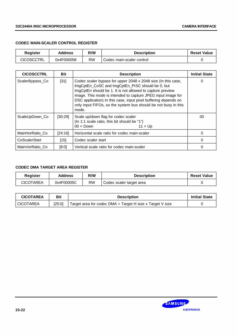
S3C2440A RISC MICROPROCESSOR CAMERA INTERFACE
23-22
CODEC MAIN-SCALER CONTROL REGISTER
Register Address R/W Description Reset Value
CICOSCCTRL 0x4F000058 RW Codec main-scaler control 0
CICOSCCTRL Bit Description Initial State
ScalerBypass_Co [31] Codec scaler bypass for upper 2048 x 2048 size (In this case,ImgCptEn_CoSC and ImgCptEn_PrSC should be 0, butImgCptEn should be 1. It is not allowed to capture previewimage. This mode is intended to capture JPEG input image forDSC application) In this case, input pixel buffering depends ononly input FIFOs, so the system bus should be not busy in thismode.
0
ScaleUpDown_Co [30:29] Scale up/down flag for codec scaler(In 1:1 scale ratio, this bit should be “1”)00 = Down 11 = Up
00
MainHorRatio_Co [24:16] Horizontal scale ratio for codec main-scaler 0
CoScalerStart [15] Codec scaler start 0
MainVerRatio_Co [8:0] Vertical scale ratio for codec main-scaler 0
CODEC DMA TARGET AREA REGISTER
Register Address R/W Description Reset Value
CICOTAREA 0x4F00005C RW Codec scaler target area 0
CICOTAREA Bit Description Initial State
CICOTAREA [25:0] Target area for codec DMA = Target H size x Target V size 0
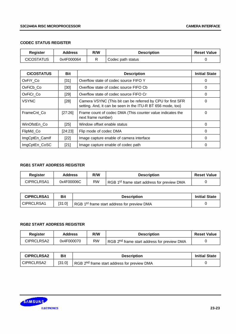
S3C2440A RISC MICROPROCESSOR CAMERA INTERFACE
23-23
CODEC STATUS REGISTER
Register Address R/W Description Reset Value
CICOSTATUS 0x4F000064 R Codec path status 0
CICOSTATUS Bit Description Initial State
OvFiY_Co [31] Overflow state of codec source FIFO Y 0
OvFiCb_Co [30] Overflow state of codec source FIFO Cb 0
OvFiCr_Co [29] Overflow state of codec source FIFO Cr 0
VSYNC [28] Camera VSYNC (This bit can be referred by CPU for first SFRsetting. And, it can be seen in the ITU-R BT 656 mode, too)
0
FrameCnt_Co [27:26] Frame count of codec DMA (This counter value indicates thenext frame number)
0
WinOfstEn_Co [25] Window offset enable status 0
FlipMd_Co [24:23] Flip mode of codec DMA 0
ImgCptEn_CamIf [22] Image capture enable of camera interface 0
ImgCptEn_CoSC [21] Image capture enable of codec path 0
RGB1 START ADDRESS REGISTER
Register Address R/W Description Reset Value
CIPRCLRSA1 0x4F00006C RW RGB 1st frame start address for preview DMA 0
CIPRCLRSA1 Bit Description Initial State
CIPRCLRSA1 [31:0] RGB 1st frame start address for preview DMA 0
RGB2 START ADDRESS REGISTER
Register Address R/W Description Reset Value
CIPRCLRSA2 0x4F000070 RW RGB 2nd frame start address for preview DMA 0
CIPRCLRSA2 Bit Description Initial State
CIPRCLRSA2 [31:0] RGB 2nd frame start address for preview DMA 0
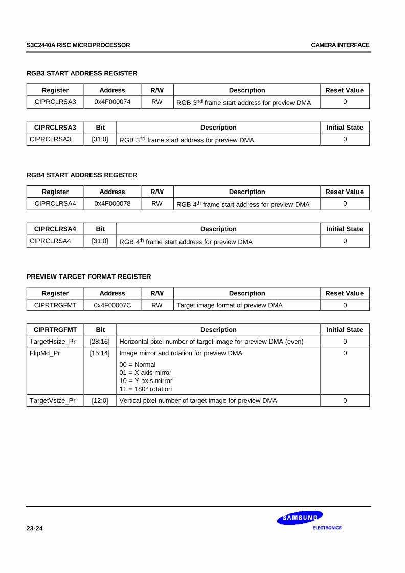
S3C2440A RISC MICROPROCESSOR CAMERA INTERFACE
23-24
RGB3 START ADDRESS REGISTER
Register Address R/W Description Reset Value
CIPRCLRSA3 0x4F000074 RW RGB 3nd frame start address for preview DMA 0
CIPRCLRSA3 Bit Description Initial State
CIPRCLRSA3 [31:0] RGB 3nd frame start address for preview DMA 0
RGB4 START ADDRESS REGISTER
Register Address R/W Description Reset Value
CIPRCLRSA4 0x4F000078 RW RGB 4th frame start address for preview DMA 0
CIPRCLRSA4 Bit Description Initial State
CIPRCLRSA4 [31:0] RGB 4th frame start address for preview DMA 0
PREVIEW TARGET FORMAT REGISTER
Register Address R/W Description Reset Value
CIPRTRGFMT 0x4F00007C RW Target image format of preview DMA 0
CIPRTRGFMT Bit Description Initial State
TargetHsize_Pr [28:16] Horizontal pixel number of target image for preview DMA (even) 0
FlipMd_Pr [15:14] Image mirror and rotation for preview DMA
00 = Normal01 = X-axis mirror10 = Y-axis mirror11 = 180° rotation
0
TargetVsize_Pr [12:0] Vertical pixel number of target image for preview DMA 0

S3C2440A RISC MICROPROCESSOR CAMERA INTERFACE
23-25
PREVIEW DMA CONTROL REGISTER
Register Address R/W Description Reset Value
CIPRCTRL 0x4F000080 RW Preview DMA control related 0
CIPRCTRL Bit Description Initial State
RGBburst1_Pr [23:19] Main burst length for preview RGB frames 0
RGBburst2_Pr [18:14] Remained burst length for preview RGB frames 0
LastIRQEn_Pr [2] 0 = Normal1 = Enable last IRQ at the end of frame capture. (This bit is cleared automatically.)
0
NOTE: All burst lengths must be one of the 2, 4, 8, 16.
Example 1: Target image size: QCIF for RGB 32-bit format (horizontal width = 176 pixels. 1 pixel = 1 word)
176 pixel = 176 word. 176 % 16 = 0 → main burst = 16, remained burst = 16
Example 2: Target image size: VGA for RGB 16-bit format (horizontal width = 640 pixels. 2 pixel = 1 word)
640 / 2 = 320 word160 % 16 = 0 → main burst = 16, remained burst = 16
PREVIEW PRE-SCALER CONTROL REGISTER 1
Register Address R/W Description Reset Value
CIPRSCPRERATIO 0x4F000084 RW Preview pre-scaler ratio control 0
CIPRSCPRERATIO Bit Description Initial State
SHfactor_Pr [31:28] Shift factor for preview pre-scaler 0
PreHorRatio_Pr [22:16] Horizontal ratio of preview pre-scaler 0
PreVerRatio_Pr [6:0] Vertical ratio of preview pre-scaler 0

S3C2440A RISC MICROPROCESSOR CAMERA INTERFACE
23-26
PREVIEW PRE-SCALER CONTROL REGISTER 2
Register Address R/W Description Reset Value
CIPRSCPREDST 0x4F000088 RW Preview pre-scaler destination format 0
CIPRSCPREDST Bit Description Initial State
PreDstWidth_Pr [27:16] Destination width for preview pre-scaler 0
PreDstHeight_Pr [11:0] Destination height for preview pre-scaler 0
PREVIEW MAIN-SCALER CONTROL REGISTER
Register Address R/W Description Reset Value
CIPRSCCTRL 0x4F00008C RW Preview main-scaler control 0
CICOSCCTRL Bit Description Initial State
Sample_Pr [31] Sampling method for format conversion.(This bit is recommended to fix 1)
0
RGBformat_Pr [30] 0 = 16-bit RGB 1 = 24-bit RGB 0
ScaleUpDown_Pr [29:28] Scale up/down flag for preview scaler(In 1:1 scale ratio, this bit should be “1”)00 = down 11 = up
00
MainHorRatio_Pr [24:16] Horizontal scale ratio for preview main-scaler 0
PrScalerStart [15] Preview scaler start 0
MainVerRatio_Pr [8:0] Vertical scale ratio for preview main-scaler 0
PREVIEW DMA TARGET AREA REGISTER
Register Address R/W Description Reset Value
CIPRTAREA 0x4F000090 RW Preview scaler target area 0
CIPRTAREA Bit Description Initial State
CIPRTAREA [25:0] Target area for preview DMA = Target H size x Target V size 0

S3C2440A RISC MICROPROCESSOR CAMERA INTERFACE
23-27
PREVIEW STATUS REGISTER
Register Address R/W Description Reset Value
CIPRSTATUS 0x4F000098 R Preview path status 0
CIPRSTATUS Bit Description Initial State
OvFiCb_Pr [31] Overflow state of preview source FIFO Cb 0
OvFiCr_Pr [30] Overflow state of preview source FIFO Cr 0
FrameCnt_Pr [27:26] Frame count of preview DMA 0
FlipMd_Pr [24:23] Flip mode of preview DMA 0
ImgCptEn_PrSC [21] Image capture enable of preview path 0
IMAGE CAPTURE ENABLE REGISTER
This register must be set at last.
Register Address R/W Description Reset Value
CIIMGCPT 0x4F0000A0 RW Image capture enable command 0
CIGCTRL Bit Description Initial State
ImgCptEn [31] Camera interface global capture enable 0
ImgCptEn_CoSc [30] Capture enable for codec scaler.This bit must be ‘0’ in scaler bypass mode.
0
ImgCptEn_PrSc [29] Capture enable for preview scalerThis bit must be ‘0’ in scaler bypass mode.
0

S3C2440A RISC MICROPROCESSOR CAMERA INTERFACE
23-28
NOTES
S3C2440A RISC MICROPROCESSOR AC97 CONTROLLER
24-1
24 AC97 CONTROLLER
OVERVIEW
The AC97 Controller Unit of the S3C2440A supports AC97 revision 2.0 features. AC97 Controller communicates withAC97 Codec using an audio controller link (AC-link). Controller sends the stereo PCM data to Codec. The externaldigital-to-analog converter (DAC) in the Codec then converts the audio sample to an analog audio waveform. Also, theController receives the stereo PCM data and the mono Mic data from the Codec and then stores them in thememories. This chapter describes the programming model for the AC97 Controller Unit. The information in thischapter requires an understanding of the AC97 revision 2.0 specifications.
NOTE
The AC97 Controller and the I2S Controller must not be used at the same time.
FEATURES
— Independent channels for stereo PCM In, stereo PCM Out, mono MIC In.
— DMA-based operation and interrupt based operation.
— All of the channels support only 16-bit samples.
— Variable sampling rate AC97 Codec interface (48 KHz and below)
— 16-bit, 16 entry FIFOs per channel
— Only Primary CODEC support
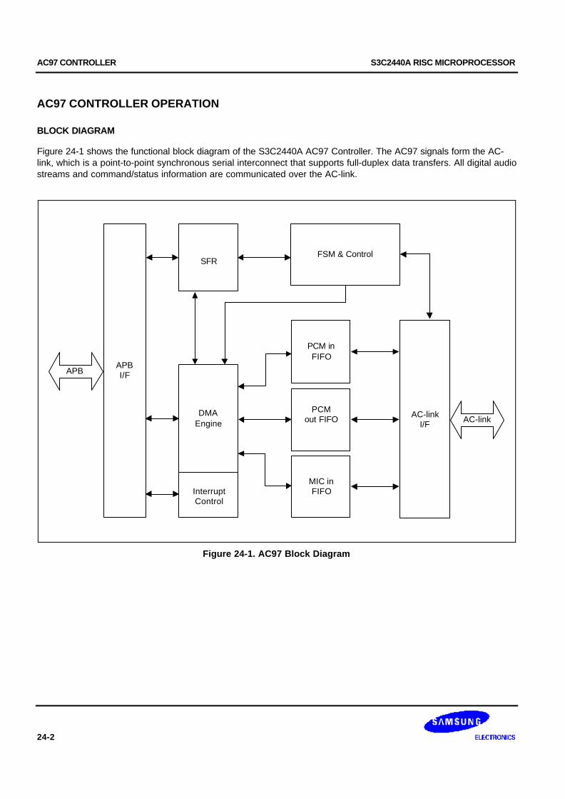
AC97 CONTROLLER S3C2440A RISC MICROPROCESSOR
24-2
AC97 CONTROLLER OPERATION
BLOCK DIAGRAM
Figure 24-1 shows the functional block diagram of the S3C2440A AC97 Controller. The AC97 signals form the AC-link, which is a point-to-point synchronous serial interconnect that supports full-duplex data transfers. All digital audiostreams and command/status information are communicated over the AC-link.
APBI/F
DMAEngine
InterruptControl
MIC inFIFO
PCMout FIFO
PCM inFIFO
SFR
AC-linkI/F
FSM & Control
APB
AC-link
Figure 24-1. AC97 Block Diagram
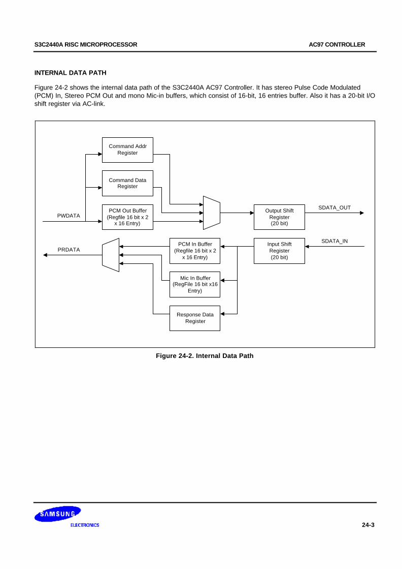
S3C2440A RISC MICROPROCESSOR AC97 CONTROLLER
24-3
INTERNAL DATA PATH
Figure 24-2 shows the internal data path of the S3C2440A AC97 Controller. It has stereo Pulse Code Modulated(PCM) In, Stereo PCM Out and mono Mic-in buffers, which consist of 16-bit, 16 entries buffer. Also it has a 20-bit I/Oshift register via AC-link.
Command AddrRegister
Command DataRegister
PCM Out Buffer(Regfile 16 bit x 2
x 16 Entry)PWDATA
Response DataRegister
Mic In Buffer(RegFile 16 bit x16
Entry)
PCM In Buffer(Regfile 16 bit x 2
x 16 Entry)PRDATA
Input ShiftRegister(20 bit)
Output ShiftRegister(20 bit)
SDATA_IN
SDATA_OUT
Figure 24-2. Internal Data Path
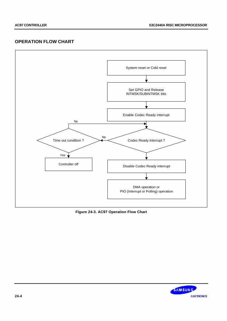
AC97 CONTROLLER S3C2440A RISC MICROPROCESSOR
24-4
OPERATION FLOW CHART
System reset or Cold reset
Set GPIO and ReleaseINTMSK/SUBINTMSK bits
Enable Codec Ready interrupt
Disable Codec Ready interrupt
DMA operation orPIO (Interrupt or Polling) operation
Controller off
Yes
No
NoCodec Ready interrupt ?Time out condition ?
Figure 24-3. AC97 Operation Flow Chart
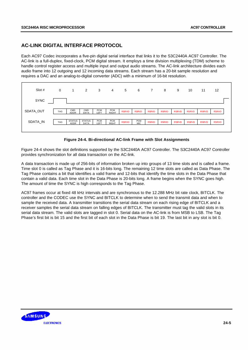
S3C2440A RISC MICROPROCESSOR AC97 CONTROLLER
24-5
AC-LINK DIGITAL INTERFACE PROTOCOL
Each AC97 Codec incorporates a five-pin digital serial interface that links it to the S3C2440A AC97 Controller. TheAC-link is a full-duplex, fixed-clock, PCM digital stream. It employs a time division multiplexing (TDM) scheme tohandle control register access and multiple input and output audio streams. The AC-link architecture divides eachaudio frame into 12 outgoing and 12 incoming data streams. Each stream has a 20-bit sample resolution andrequires a DAC and an analog-to-digital converter (ADC) with a minimum of 16-bit resolution.
SYNC
SDATA_OUT
SDATA_IN
Slot #
TAG CMDADDR
CMDDATA
PCM PCM RSRVD
TAG STATUSADDR
STATUSDATA
PCMLEFT
PCMRIGHT
0 1 2 3 4 5 6 7 8 9 10 11 12
RSRVDRSRVDRSRVDRSRVDRSRVDRSRVDRSRVD
RSRVD RSRVD RSRVD RSRVD RSRVD RSRVD RSRVDPCMMIC
LEFT RIGHT
Figure 24-4. Bi-directional AC-link Frame with Slot Assignments
Figure 24-4 shows the slot definitions supported by the S3C2440A AC97 Controller. The S3C2440A AC97 Controllerprovides synchronization for all data transaction on the AC-link.
A data transaction is made up of 256-bits of information broken up into groups of 13 time slots and is called a frame.Time slot 0 is called as Tag Phase and it is 16-bits long. The remaining 12 time slots are called as Data Phase. TheTag Phase contains a bit that identifies a valid frame and 12-bits that identify the time slots in the Data Phase thatcontain a valid data. Each time slot in the Data Phase is 20-bits long. A frame begins when the SYNC goes high.The amount of time the SYNC is high corresponds to the Tag Phase.
AC97 frames occur at fixed 48 kHz intervals and are synchronous to the 12.288 MHz bit rate clock, BITCLK. Thecontroller and the CODEC use the SYNC and BITCLK to determine when to send the transmit data and when tosample the received data. A transmitter transitions the serial data stream on each rising edge of BITCLK and areceiver samples the serial data stream on falling edges of BITCLK. The transmitter must tag the valid slots in itsserial data stream. The valid slots are tagged in slot 0. Serial data on the AC-link is from MSB to LSB. The TagPhase’s first bit is bit 15 and the first bit of each slot in the Data Phase is bit 19. The last bit in any slot is bit 0.

AC97 CONTROLLER S3C2440A RISC MICROPROCESSOR
24-6
AC-LINK OUTPUT FRAME (SDATA_OUT)
SDATA_OUT
BIT_CLK
SYNCAC '97 samples SYNC assertion here
AC '97 Controller samples first SDATA_OUT bit of frame here
END of previous Audio Frame
ValidFrame
Slot(1) Slot(2) Slot(12) "0" ID1 ID0 19 0
Tag Phase Data Phase
19 0
START of Data phase Slot# 1 END of Data FrameSlot# 12
48kHz
12.288MHz
Figure 24-5. AC-link Output Frame
AC-LINK INPUT FRAME (SDATA_IN)
SDATA_OUT
BIT_CLK
SYNCAC '97 samples SYNC assertion here
AC '97 Controller samples first SDATA_IN bit of frame here
END of previous Audio Frame
CodecReady Slot(1) Slot(2) Slot(12) "0" "0" "0" 19 0
Tag Phase Data Phase
19 0
START of Data phaseSlot# 1
END of Data FrameSlot# 12
Figure 24-6. AC-link Input Frame
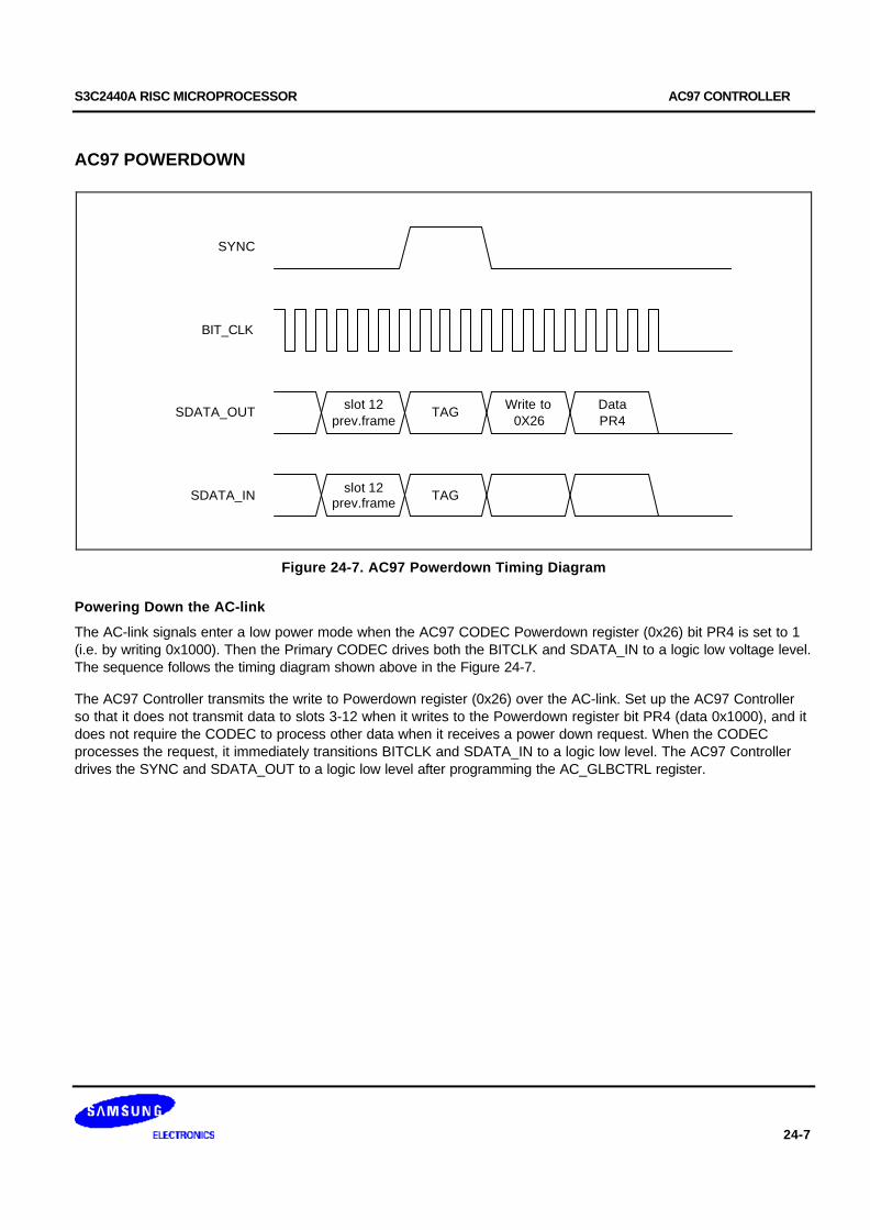
S3C2440A RISC MICROPROCESSOR AC97 CONTROLLER
24-7
AC97 POWERDOWN
SDATA_OUT
SDATA_IN
BIT_CLK
SYNC
slot 12prev.frame
Write to0X26
slot 12prev.frame
TAG
TAG
DataPR4
Figure 24-7. AC97 Powerdown Timing Diagram
Powering Down the AC-link
The AC-link signals enter a low power mode when the AC97 CODEC Powerdown register (0x26) bit PR4 is set to 1(i.e. by writing 0x1000). Then the Primary CODEC drives both the BITCLK and SDATA_IN to a logic low voltage level.The sequence follows the timing diagram shown above in the Figure 24-7.
The AC97 Controller transmits the write to Powerdown register (0x26) over the AC-link. Set up the AC97 Controllerso that it does not transmit data to slots 3-12 when it writes to the Powerdown register bit PR4 (data 0x1000), and itdoes not require the CODEC to process other data when it receives a power down request. When the CODECprocesses the request, it immediately transitions BITCLK and SDATA_IN to a logic low level. The AC97 Controllerdrives the SYNC and SDATA_OUT to a logic low level after programming the AC_GLBCTRL register.
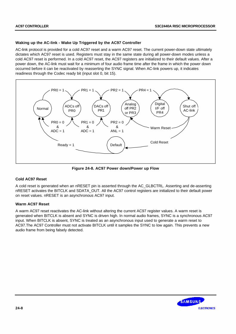
AC97 CONTROLLER S3C2440A RISC MICROPROCESSOR
24-8
Waking up the AC-link - Wake Up Triggered by the AC97 Controller
AC-link protocol is provided for a cold AC97 reset and a warm AC97 reset. The current power-down state ultimatelydictates which AC97 reset is used. Registers must stay in the same state during all power-down modes unless acold AC97 reset is performed. In a cold AC97 reset, the AC97 registers are initialized to their default values. After apower down, the AC-link must wait for a minimum of four audio frame time after the frame in which the power downoccurred before it can be reactivated by reasserting the SYNC signal. When AC-link powers up, it indicatesreadiness through the Codec ready bit (input slot 0, bit 15).
Analogoff PR2or PR3
DigitalI/F offPR4
Shut offAC-link
DACs offPR1
ADCs offPR0Normal
DefaultReady = 1
PR0 = 0&
ADC = 1
PR1 = 0&
ADC = 1
PR2 = 0&
ANL = 1Warm Reset
Cold Reset
PR0 = 1 PR1 = 1 PR2 = 1 PR4 = 1
Figure 24-8. AC97 Power down/Power up Flow
Cold AC97 Reset
A cold reset is generated when an nRESET pin is asserted through the AC_GLBCTRL. Asserting and de-assertingnRESET activates the BITCLK and SDATA_OUT. All the AC97 control registers are initialized to their default poweron reset values. nRESET is an asynchronous AC97 input.
Warm AC97 Reset
A warm AC97 reset reactivates the AC-link without altering the current AC97 register values. A warm reset isgenerated when BITCLK is absent and SYNC is driven high. In normal audio frames, SYNC is a synchronous AC97input. When BITCLK is absent, SYNC is treated as an asynchronous input used to generate a warm reset toAC97.The AC97 Controller must not activate BITCLK until it samples the SYNC to low again. This prevents a newaudio frame from being falsely detected.
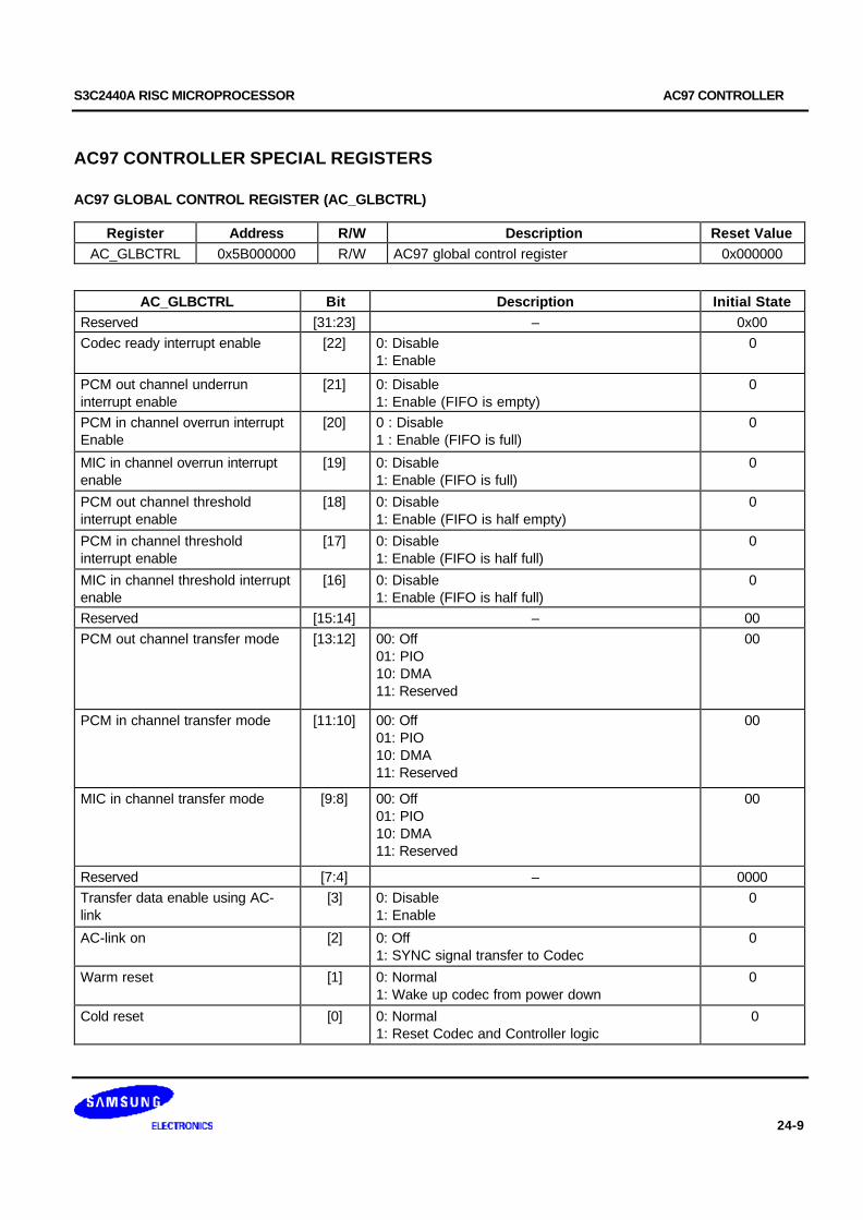
S3C2440A RISC MICROPROCESSOR AC97 CONTROLLER
24-9
AC97 CONTROLLER SPECIAL REGISTERS
AC97 GLOBAL CONTROL REGISTER (AC_GLBCTRL)
Register Address R/W Description Reset ValueAC_GLBCTRL 0x5B000000 R/W AC97 global control register 0x000000
AC_GLBCTRL Bit Description Initial StateReserved [31:23] – 0x00Codec ready interrupt enable [22] 0: Disable
1: Enable0
PCM out channel underruninterrupt enable
[21] 0: Disable1: Enable (FIFO is empty)
0
PCM in channel overrun interruptEnable
[20] 0 : Disable1 : Enable (FIFO is full)
0
MIC in channel overrun interruptenable
[19] 0: Disable1: Enable (FIFO is full)
0
PCM out channel thresholdinterrupt enable
[18] 0: Disable1: Enable (FIFO is half empty)
0
PCM in channel thresholdinterrupt enable
[17] 0: Disable1: Enable (FIFO is half full)
0
MIC in channel threshold interruptenable
[16] 0: Disable1: Enable (FIFO is half full)
0
Reserved [15:14] – 00PCM out channel transfer mode [13:12] 00: Off
01: PIO10: DMA11: Reserved
00
PCM in channel transfer mode [11:10] 00: Off01: PIO10: DMA11: Reserved
00
MIC in channel transfer mode [9:8] 00: Off01: PIO10: DMA11: Reserved
00
Reserved [7:4] – 0000Transfer data enable using AC-link
[3] 0: Disable1: Enable
0
AC-link on [2] 0: Off1: SYNC signal transfer to Codec
0
Warm reset [1] 0: Normal1: Wake up codec from power down
0
Cold reset [0] 0: Normal1: Reset Codec and Controller logic
0

AC97 CONTROLLER S3C2440A RISC MICROPROCESSOR
24-10
AC97 GLOBAL STATUS REGISTER (AC_GLBSTAT)
Register Address R/W Description Reset Value
AC_GLBSTAT 0x5B000004 R AC97 global status register 0x00000000
AC_GLBSTAT Bit Description Initial State
Reserved [31:23] – 0x00
Codec ready interrupt [22] 0: Not requested 1: Requested 0
PCM out channel underrun interrupt [21] 0: Not requested 1: Requested 0
PCM in channel overrun Interrupt [20] 0: Not requested 1: Requested 0
MIC in channel overrun interrupt [19] 0: Not requested 1: Requested 0
PCM out channel threshold interrupt [18] 0: Not requested 1: Requested 0
PCM in channel threshold interrupt [17] 0: Not requested 1: Requested 0
MIC in channel threshold interrupt [16] 0: Not requested 1: Requested 0
Reserved [15:3] – 0x000
Controller main state [2:0] 000: Idle 001: Init 010: Ready011: Active 100: LP 101: Warm
000
AC97 CODEC COMMAND REGISTER (AC_CODEC_CMD)
Register Address R/W Description Reset Value
AC_CODEC_CMD 0x5B000008 R/W AC97 codec command register 0x00000000
AC_CODEC_CMD Bit Description Initial State
Reserved [31:24] – 0x00
Read enable [23] 0: Command write (NOTE) 1: Status read
0
Address [22:16] CODEC command address 0x00
Data [15:0] CODEC command data 0x0000
NOTE: When the commands are written on the AC_CODDEC_CMD register, it is recommended that the delay timebetween the command and the next command is more than 1/48 Hz.

S3C2440A RISC MICROPROCESSOR AC97 CONTROLLER
24-11
AC97 CODEC STATUS REGISTER (AC_CODEC_STAT)
Register Address R/W Description Reset Value
AC_CODEC_STAT 0x5B00000C R AC97 codec status register 0x00000000
AC_CODEC_STAT Bit Description Initial State
Reserved [31:23] – 0x00
Address [22:16] CODEC status address 0x00
Data [15:0] CODEC status data 0x0000
NTOES:If you want to read data from AC97 codec register via the AC_CODEC_STAT register, you should follow these steps.1. Write command address and data on the AC_CODEC_CMD register with Bit [23] =1.2. Have a delay time.3. Read command address and data from AC_CODEC_STAT register.
AC97 PCM OUT/IN CHANNEL FIFO ADDRESS REGISTER (AC_PCMADDR)
Register Address R/W Description Reset Value
AC_PCMADDR 0x5B000010 R AC97 PCM out/in channel FIFO addressregister
0x00000000
AC_PCMADDR Bit Description Initial State
Reserved [31:28] – 0000
Out read address [27:24] PCM out channel FIFO read address 0000
Reserved [23:20] – 0000
In read address [19:16] PCM in channel FIFO read address 0000
Reserved [15:12] – 0000
Out write address [11:8] PCM out channel FIFO write address 0000
Reserved [7:4] – 0000
In write address [3:0] PCM in channel FIFO write address 0000

AC97 CONTROLLER S3C2440A RISC MICROPROCESSOR
24-12
AC97 MIC IN CHANNEL FIFO ADDRESS REGISTER (AC_MICADDR)
Register Address R/W Description Reset Value
AC_MICADDR 0x5B000014 R AC97 MIC in channel FIFO address register 0x00000000
AC_MICADDR Bit Description Initial State
Reserved [31:20] – 0000
Read Address [19:16] MIC in channel FIFO read address 0000
Reserved [15:4] – 0x000
Write Address [3:0] MIC in channel FIFO write address 0000
AC97 PCM OUT/IN CHANNEL FIFO DATA REGISTER (AC_PCMDATA)
Register Address R/W Description Reset Value
AC_PCMDATA 0x5B000018 R/W AC97 PCM out/in channel FIFO data register 0x00000000
AC_PCMDATA Bit Description Initial State
Left Data [31:16] PCM out/in left channel FIFO dataRead: PCM in left channelWrite: PCM out left channel
0x0000
Right Data [15:0] PCM out/in right channel FIFO dataRead: PCM in right channelWrite: PCM out right channel
0x0000
AC97 MIC IN CHANNEL FIFO DATA REGISTER (AC_MICDATA)
Register Address R/W Description Reset Value
AC_MICDATA 0x5B00001C R/W AC97 MIC in channel FIFO data register 0x00000000
AC_MICDATA Bit Description Initial State
Reserved [31:16] – 0x0000
Mono Data [15:0] MIC in mono channel FIFO data 0x0000
S3C2440A RISC MICROPROCESSOR BUS PRIORITIES
25-1
25 BUS PRIORITIES
OVERVIEW
The bus arbitration logic determines the priorities of bus masters. It supports a combination of rotation priority modeand fixed priority mode.
BUS PRIORITY MAP
The S3C2440A holds 13 bus masters. They include DRAM refresh controller, LCD_DMA, CAMIF DMA, DMA0,DMA1, DMA2, DMA3, USB_HOST_DMA, EXT_BUS_MASTER, Test interface controller (TIC) and ARM920T. Thefollowing list shows the priorities among these bus masters after a reset:
1. DRAM refresh controller
2. LCD_DMA
3. CAMIF codec DMA
4. CAMIF preview DMA
5. DMA0
6. DMA1
7. DMA2
8. DMA3
9. USB host DMA
10. External bus master
11. TIC
12. ARM920T
13. Reserved
Among these bus masters, the four DMAs (DMA0, DMA1, DMA2 and DMA3) operate under rotation priority, whilethe others run under fixed priority.

BUS PRIORITIES S3C2440A RISC MICROPROCESSOR
25-2
NOTES
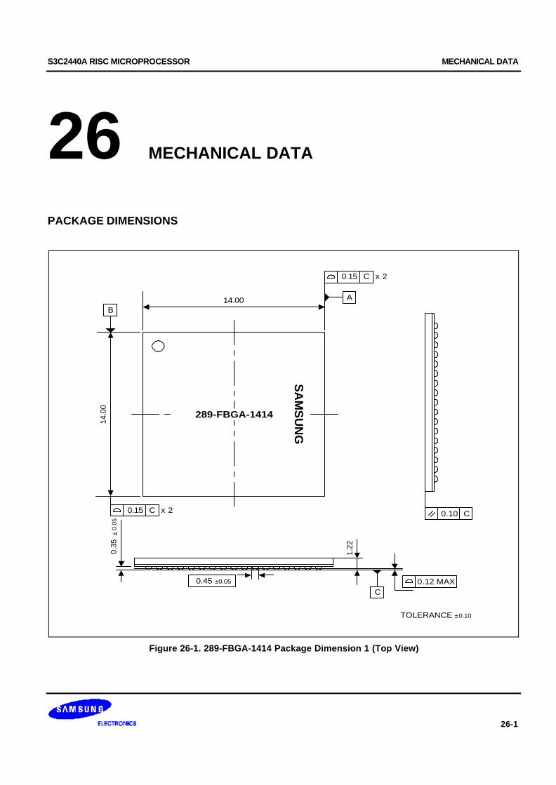
S3C2440A RISC MICROPROCESSOR MECHANICAL DATA
26-1
26 MECHANICAL DATA
PACKAGE DIMENSIONS
14.00
14.0
00.
35 +
0.0
5
1.22
289-FBGA-1414
0.45 ±0.05
C0.12 MAX
0.10 C
A
B
0.15
TOLERANCE ±0.10
x 2
0.15 x 2C
C
SA
MS
UN
G
Figure 26-1. 289-FBGA-1414 Package Dimension 1 (Top View)
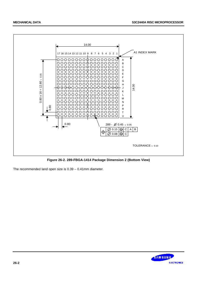
MECHANICAL DATA S3C2440A RISC MICROPROCESSOR
26-2
A1 INDEX MARK
0.80
x 1
6 =
12.8
0 ±
0.0
5
14.0
0
0.80
0.80
ABCDEFGHJKLMNPRTU
891011121314151617 567 1234
14.00
0.15
0.08
M
M
C
C
A B
289 - 0.45 ± 0.05
TOLERANCE ± 0.10
Figure 26-2. 289-FBGA-1414 Package Dimension 2 (Bottom View)
The recommended land open size is 0.39 – 0.41mm diameter.

S3C2440A RISC MICROPROCESSOR ELECTRICAL DATA
27-1
27 ELECTRICAL DATA
ABSOLUTE MAXIMUM RATINGS
Table 27-1. Absolute Maximum Rating
Parameter Symbol Rating Unit
DC Supply Voltage VDDi 1.2V VDD 1.8 V
VDDOP 3.3V VDD 4.8
VDDMOP 1.8V/2.5V/3.0V/3.3V VDD 4.8
VDDRTC 1.8V/2.5V/3.0V/3.3V VDD 4.5
VDDADC 3.3V VDD 4.8
DC Input Voltage VIN 3.3V Input buffer 4.8
3.3V Interface / 5V Tolerant input buffer 6.5
DC Output Voltage VOUT 3.3V Output buffer 4.8
DC Input (Latch-up) Current IIN ± 200 mA
Storage Temperature TSTG – 65 to 150 oC
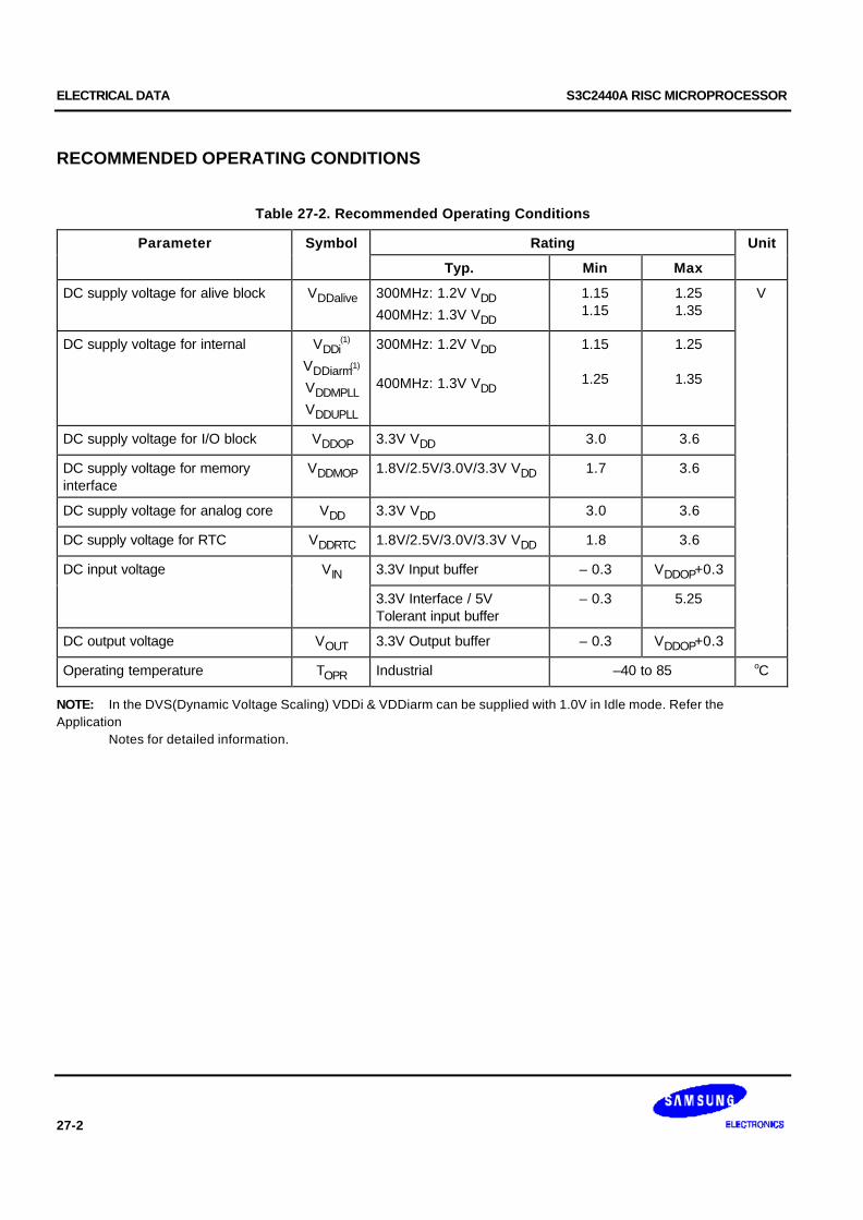
ELECTRICAL DATA S3C2440A RISC MICROPROCESSOR
27-2
RECOMMENDED OPERATING CONDITIONS
Table 27-2. Recommended Operating Conditions
Parameter Symbol Rating Unit
Typ. Min Max
DC supply voltage for alive block VDDalive 300MHz: 1.2V VDD400MHz: 1.3V VDD
1.151.15
1.251.35
V
DC supply voltage for internal VDDi(1)
VDDiarm(1)
VDDMPLLVDDUPLL
300MHz: 1.2V VDD
400MHz: 1.3V VDD
1.15
1.25
1.25
1.35
DC supply voltage for I/O block VDDOP 3.3V VDD 3.0 3.6
DC supply voltage for memoryinterface
VDDMOP 1.8V/2.5V/3.0V/3.3V VDD 1.7 3.6
DC supply voltage for analog core VDD 3.3V VDD 3.0 3.6
DC supply voltage for RTC VDDRTC 1.8V/2.5V/3.0V/3.3V VDD 1.8 3.6
DC input voltage VIN 3.3V Input buffer – 0.3 VDDOP+0.3
3.3V Interface / 5VTolerant input buffer
– 0.3 5.25
DC output voltage VOUT 3.3V Output buffer – 0.3 VDDOP+0.3
Operating temperature TOPR Industrial –40 to 85 oC
NOTE: In the DVS(Dynamic Voltage Scaling) VDDi & VDDiarm can be supplied with 1.0V in Idle mode. Refer theApplication
Notes for detailed information.
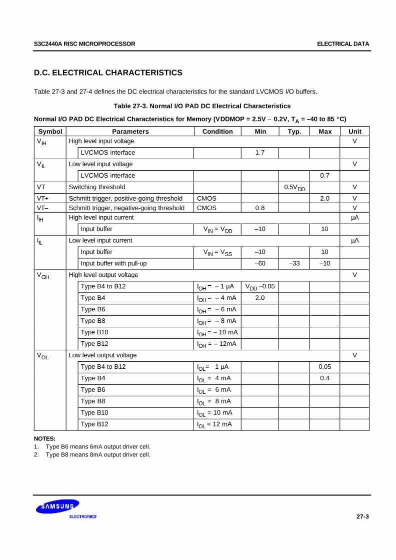
S3C2440A RISC MICROPROCESSOR ELECTRICAL DATA
27-3
D.C. ELECTRICAL CHARACTERISTICS
Table 27-3 and 27-4 defines the DC electrical characteristics for the standard LVCMOS I/O buffers.
Table 27-3. Normal I/O PAD DC Electrical Characteristics
Normal I/O PAD DC Electrical Characteristics for Memory (VDDMOP = 2.5V ± 0.2V, TA = –40 to 85 °C)
Symbol Parameters Condition Min Typ. Max UnitVIH High level input voltage V
LVCMOS interface 1.7
VIL Low level input voltage V
LVCMOS interface 0.7
VT Switching threshold 0.5VDD V
VT+ Schmitt trigger, positive-going threshold CMOS 2.0 VVT– Schmitt trigger, negative-going threshold CMOS 0.8 VIIH High level input current µA
Input buffer VIN = VDD –10 10
IIL Low level input current µA
Input buffer VIN = VSS –10 10
Input buffer with pull-up –60 –33 –10
VOH High level output voltage V
Type B4 to B12 IOH = – 1 µA VDD –0.05
Type B4 IOH = – 4 mA 2.0
Type B6 IOH = – 6 mA
Type B8 IOH = – 8 mA
Type B10 IOH = – 10 mA
Type B12 IOH = – 12mA
VOL Low level output voltage V
Type B4 to B12 IOL= 1 µA 0.05
Type B4 IOL = 4 mA 0.4
Type B6 IOL = 6 mA
Type B8 IOL = 8 mA
Type B10 IOL = 10 mA
Type B12 IOL = 12 mA
NOTES:1. Type B6 means 6mA output driver cell.2. Type B8 means 8mA output driver cell.

ELECTRICAL DATA S3C2440A RISC MICROPROCESSOR
27-4
Normal I/O PAD DC Electrical Characteristics for Memory (VDDMOP=3.0V±0.3V, 3.3V±0.3V, TA= –40 to 85 °C)
Symbol Parameters Condition Min Typ. Max Unit
VIH High level input voltage V
LVCMOS interface 2.0
VIL Low level input voltage V
LVCMOS interface 0.8
VT Switching threshold 0.5VDD V
VT+ Schmitt trigger, positive-going threshold CMOS 2.0 V
VT– Schmitt trigger, negative-going threshold CMOS 0.8 V
IIH High level input current µA
Input buffer VIN = VDD –10 10
IIL Low level input current µA
Input buffer VIN = VSS –10 10
Input buffer with pull-up –60 –33 –10
VOH High level output voltage V
Type B4 to B12 IOH = – 1 µA VDD –0.05
Type B4 IOH = – 4 mA 2.4
Type B6 IOH = – 6 mA
Type B8 IOH = – 8 mA
Type B10 IOH = –10 mA
Type B12 IOH = –12 mA
VOL Low level output voltage V
Type B4 to B12 IOL = 1 µA 0.05
Type B4 IOL = 4 mA 0.4
Type B6 IOL = 6 mA
Type B8 IOL = 8 mA
Type B10 IOL = 10 mA
Type B12 IOL = 12 mA
NOTES:1. Type B6 means 6mA output driver cell.2. Type B8 means 8mA output driver cell.3. Type B12 means 12mA output driver cells.
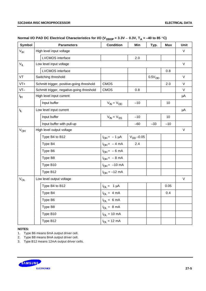
S3C2440A RISC MICROPROCESSOR ELECTRICAL DATA
27-5
Normal I/O PAD DC Electrical Characteristics for I/O (VDDOP = 3.3V ± 0.3V, TA = –40 to 85 °C)
Symbol Parameters Condition Min Typ. Max Unit
VIH High level input voltage V
LVCMOS interface 2.0
VIL Low level input voltage V
LVCMOS interface 0.8
VT Switching threshold 0.5VDD V
VT+ Schmitt trigger, positive-going threshold CMOS 2.0 V
VT– Schmitt trigger, negative-going threshold CMOS 0.8 V
IIH High level input current µA
Input buffer VIN = VDD –10 10
IIL Low level input current µA
Input buffer VIN = VSS –10 10
Input buffer with pull-up –60 –33 –10
VOH High level output voltage V
Type B4 to B12 IOH = – 1 µA VDD –0.05
Type B4 IOH = – 4 mA 2.4
Type B6 IOH = – 6 mA
Type B8 IOH = – 8 mA
Type B10 IOH = –10 mA
Type B12 IOH = –12 mA
VOL Low level output voltage V
Type B4 to B12 IOL = 1 µA 0.05
Type B4 IOL = 4 mA 0.4
Type B6 IOL = 6 mA
Type B8 IOL = 8 mA
Type B10 IOL = 10 mA
Type B12 IOL = 12 mA
NOTES:1. Type B6 means 6mA output driver cell.2. Type B8 means 8mA output driver cell.3. Type B12 means 12mA output driver cells.
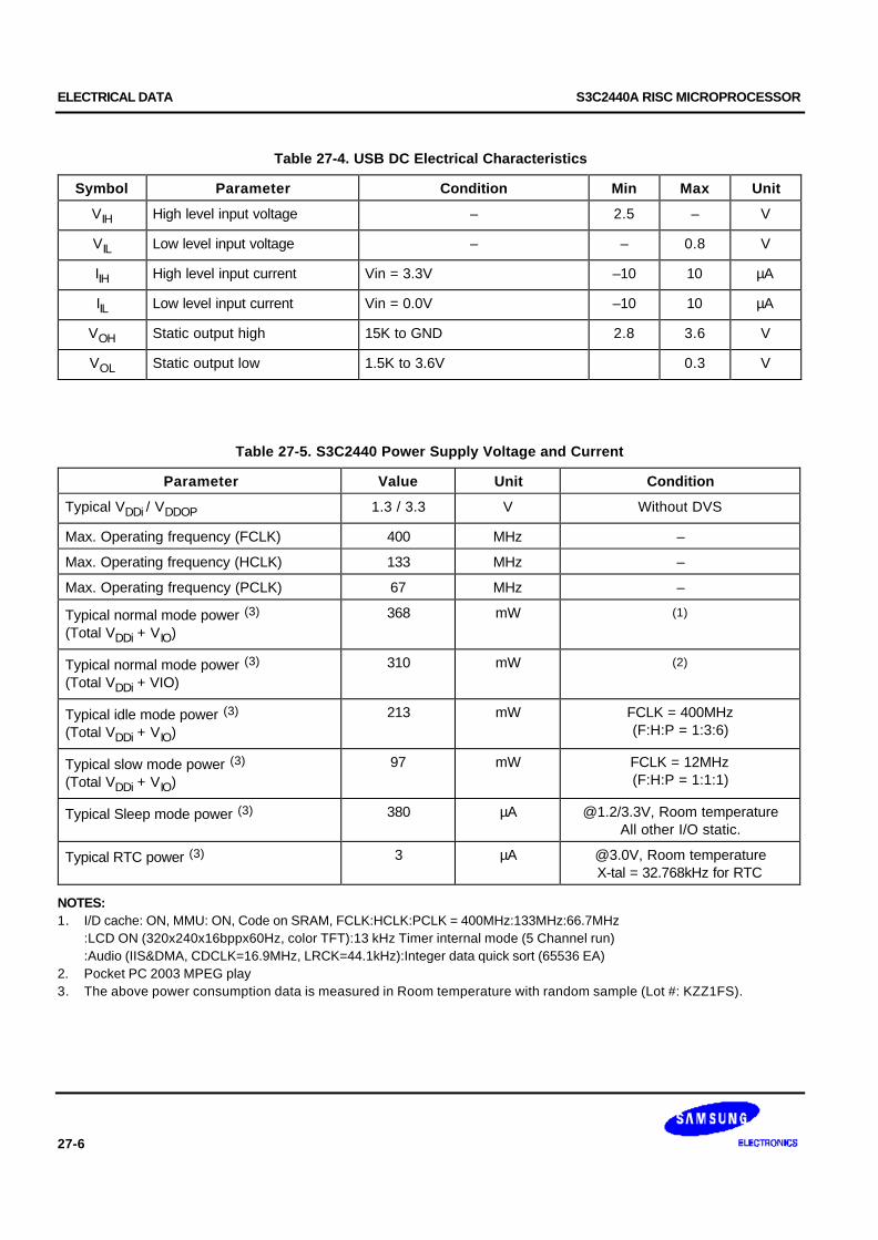
ELECTRICAL DATA S3C2440A RISC MICROPROCESSOR
27-6
Table 27-4. USB DC Electrical Characteristics
Symbol Parameter Condition Min Max Unit
VIH High level input voltage – 2.5 – V
VIL Low level input voltage – – 0.8 V
IIH High level input current Vin = 3.3V –10 10 µA
IIL Low level input current Vin = 0.0V –10 10 µA
VOH Static output high 15K to GND 2.8 3.6 V
VOL Static output low 1.5K to 3.6V 0.3 V
Table 27-5. S3C2440 Power Supply Voltage and Current
Parameter Value Unit Condition
Typical VDDi / VDDOP 1.3 / 3.3 V Without DVS
Max. Operating frequency (FCLK) 400 MHz –
Max. Operating frequency (HCLK) 133 MHz –
Max. Operating frequency (PCLK) 67 MHz –
Typical normal mode power (3)
(Total VDDi + VIO)368 mW (1)
Typical normal mode power (3)
(Total VDDi + VIO)310 mW (2)
Typical idle mode power (3)
(Total VDDi + VIO)213 mW FCLK = 400MHz
(F:H:P = 1:3:6)
Typical slow mode power (3)
(Total VDDi + VIO)97 mW FCLK = 12MHz
(F:H:P = 1:1:1)
Typical Sleep mode power (3) 380 µA @1.2/3.3V, Room temperatureAll other I/O static.
Typical RTC power (3) 3 µA @3.0V, Room temperatureX-tal = 32.768kHz for RTC
NOTES:1. I/D cache: ON, MMU: ON, Code on SRAM, FCLK:HCLK:PCLK = 400MHz:133MHz:66.7MHz
:LCD ON (320x240x16bppx60Hz, color TFT):13 kHz Timer internal mode (5 Channel run):Audio (IIS&DMA, CDCLK=16.9MHz, LRCK=44.1kHz):Integer data quick sort (65536 EA)
2. Pocket PC 2003 MPEG play3. The above power consumption data is measured in Room temperature with random sample (Lot #: KZZ1FS).

S3C2440A RISC MICROPROCESSOR ELECTRICAL DATA
27-7
400Mhz Power consumption
87mW88mW
139mW
68mW
0
50
100
150
200
250
Without DVS With DVS
Item
[mW
]
Core Power51% Down
Total Power32% Down
VDD_Core
VDD_IO
Figure 27-1. Power Consumption Example Comparison when Applied DVS Scheme
NOTE: (Condition) Current measure condition: Play Battlife.wma(bit rate=64kbps) on PPC2003 SMDK2440.Core power:Without DVS : VDDiarm/VDDi/VDDupll/VDDmpll/VDDalive = 1.3Vusing DVS : VDDiarm/VDDi = 1.3V ó 1.0V, VDDupll/VDDmpll/VDDalive = 1.3VI/O Power : VDDOP/VDDMOP/VDDRTC/VDDADC=3.3VRefer the Application notes for more information about DVS.
Table 27-6. Typical Current Decrease by CLKCON Register
FCLK:HCLK:PCLK = 300:100:50MHz, 1.2V (Random sample)
(Unit: mA)
Peripherals NFC LCD USBH USBD Timer SDI UART RTC ADC IIC IIS SPI Camera Total
Current 1.7 2.8 0.37 0.79 0.32 1.0 2.7 0.45 0.26 0.32 0.78 0.16 14.25 26.26
NOTE: This table includes power consumption of each peripheral. For example, If you do not use Camera and have turnedoff the Camera block by CLKCON register, then you can save the 14.25mA of internal block.
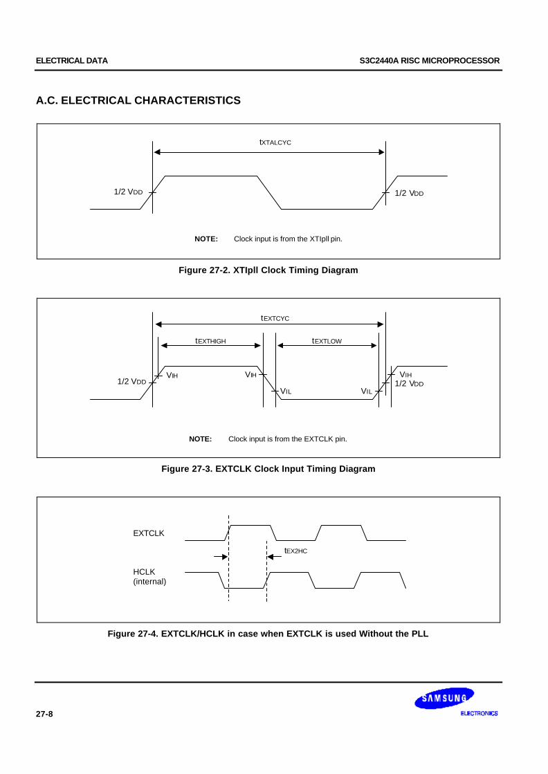
ELECTRICAL DATA S3C2440A RISC MICROPROCESSOR
27-8
A.C. ELECTRICAL CHARACTERISTICS
1/2 VDD1/2 VDD
tXTALCYC
NOTE: Clock input is from the XTIpll pin.
Figure 27-2. XTIpll Clock Timing Diagram
tEXTHIGH
VIH1/2 VDD
VILVIL
VIHVIH1/2 VDD
tEXTLOW
tEXTCYC
NOTE: Clock input is from the EXTCLK pin.
Figure 27-3. EXTCLK Clock Input Timing Diagram
HCLK(internal)
EXTCLK
tEX2HC
Figure 27-4. EXTCLK/HCLK in case when EXTCLK is used Without the PLL
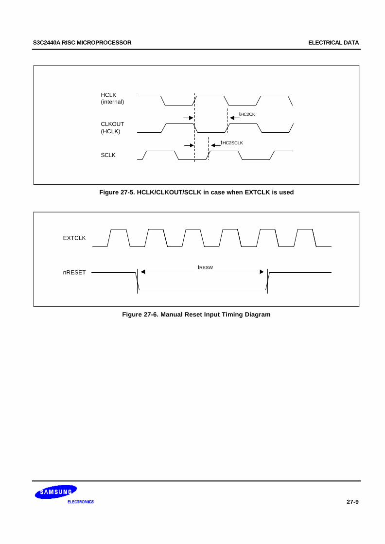
S3C2440A RISC MICROPROCESSOR ELECTRICAL DATA
27-9
HCLK(internal)
SCLK
CLKOUT(HCLK)
tHC2CK
tHC2SCLK
Figure 27-5. HCLK/CLKOUT/SCLK in case when EXTCLK is used
EXTCLK
tRESWnRESET
Figure 27-6. Manual Reset Input Timing Diagram
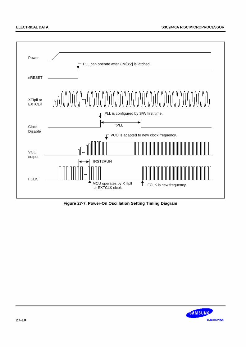
ELECTRICAL DATA S3C2440A RISC MICROPROCESSOR
27-10
nRESET
XTIpll orEXTCLK
VCOoutput
MCU operates by XTIpll or EXTCLK clcok.
ClockDisable
tPLL
FCLK is new frequency.
Power
PLL can operate after OM[3:2] is latched.
PLL is configured by S/W first time.
VCO is adapted to new clock frequency.
FCLK
...
...
...
tRST2RUN
Figure 27-7. Power-On Oscillation Setting Timing Diagram

S3C2440A RISC MICROPROCESSOR ELECTRICAL DATA
27-11
XTIpll
VCOOutput
ClockDisable
FCLK
Several slow clocks (XTIpll or EXTCLK)
Power_OFF mode is initiated.
tOSC2
EXTCLK
Figure 27-8. Sleep Mode Return Oscillation Setting Timing Diagram
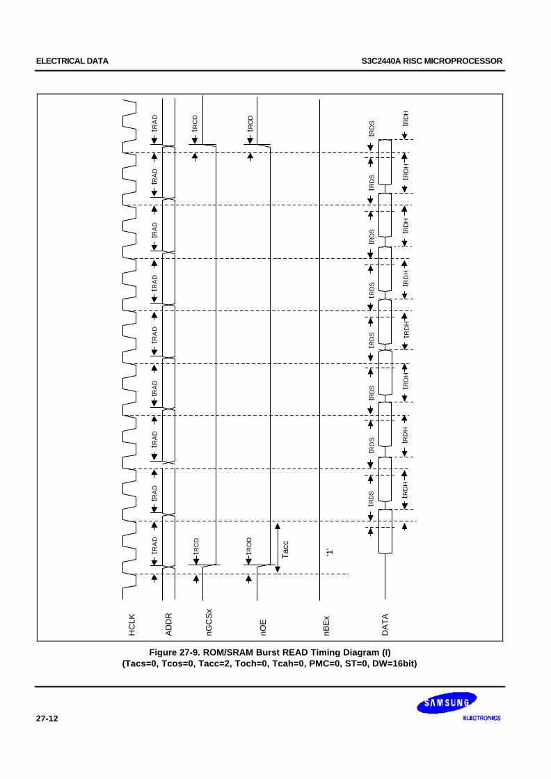
ELECTRICAL DATA S3C2440A RISC MICROPROCESSOR
27-12
HC
LK
nGC
Sx
tRA
D
nOE
DA
TA
AD
DR
nBE
x
tRC
D
tRO
DtR
OD
tRC
D
Tac
c
tRA
DtR
AD
tRA
DtR
AD
tRA
DtR
AD
tRA
DtR
AD
tRD
S tRD
H
tRD
S tRD
H
tRD
S tRD
H
tRD
S tRD
H
tRD
S tRD
H
tRD
S tRD
H
tRD
S tRD
H
tRD
S tRD
H
'1'
Figure 27-9. ROM/SRAM Burst READ Timing Diagram (I)(Tacs=0, Tcos=0, Tacc=2, Toch=0, Tcah=0, PMC=0, ST=0, DW=16bit)
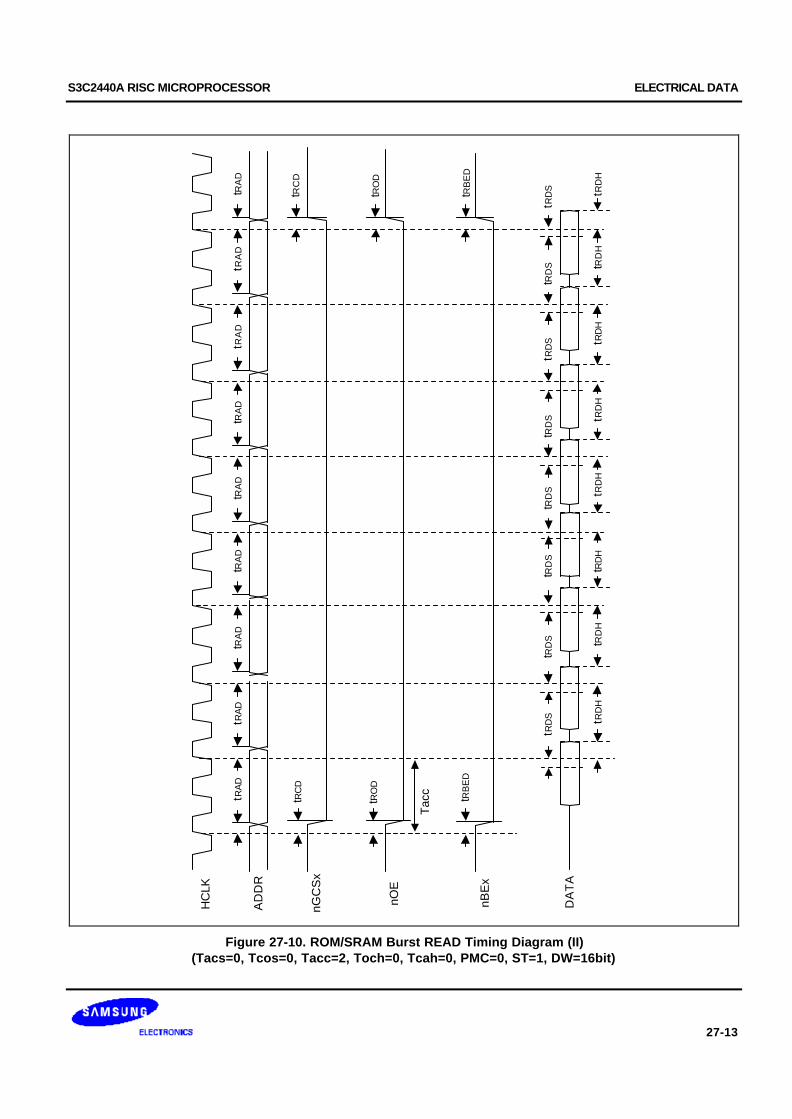
S3C2440A RISC MICROPROCESSOR ELECTRICAL DATA
27-13
HC
LK
nGC
Sx
tRA
D
nOE
DA
TA
AD
DR
nBE
x
tRC
D
tRO
DtR
OD
tRC
D
tRB
ED
tRB
ED
Tac
c
tRA
DtR
AD
tRA
DtR
AD
tRA
DtR
AD
tRA
DtR
AD
tRD
S tRD
H
tRD
S tRD
H
tRD
S
tRD
H
tRD
S tRD
H
tRD
S tRD
H
tRD
S tRD
H
tRD
S tRD
H
tRD
S tRD
H
Figure 27-10. ROM/SRAM Burst READ Timing Diagram (II)(Tacs=0, Tcos=0, Tacc=2, Toch=0, Tcah=0, PMC=0, ST=1, DW=16bit)
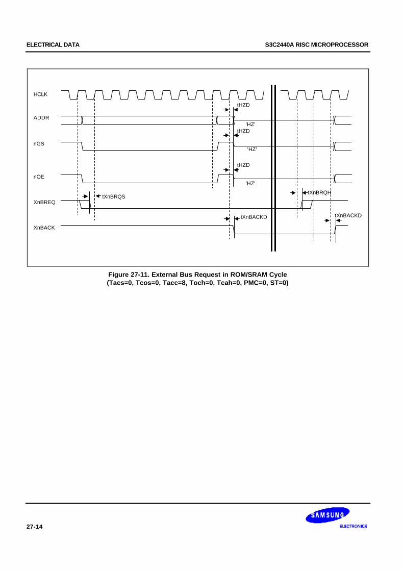
ELECTRICAL DATA S3C2440A RISC MICROPROCESSOR
27-14
HCLK
nGS
nOE
ADDR
tXnBRQSXnBREQ
tXnBRQH
XnBACK
'HZ'
'HZ'
'HZ'
tXnBACKD tXnBACKD
tHZD
tHZD
tHZD
Figure 27-11. External Bus Request in ROM/SRAM Cycle(Tacs=0, Tcos=0, Tacc=8, Toch=0, Tcah=0, PMC=0, ST=0)
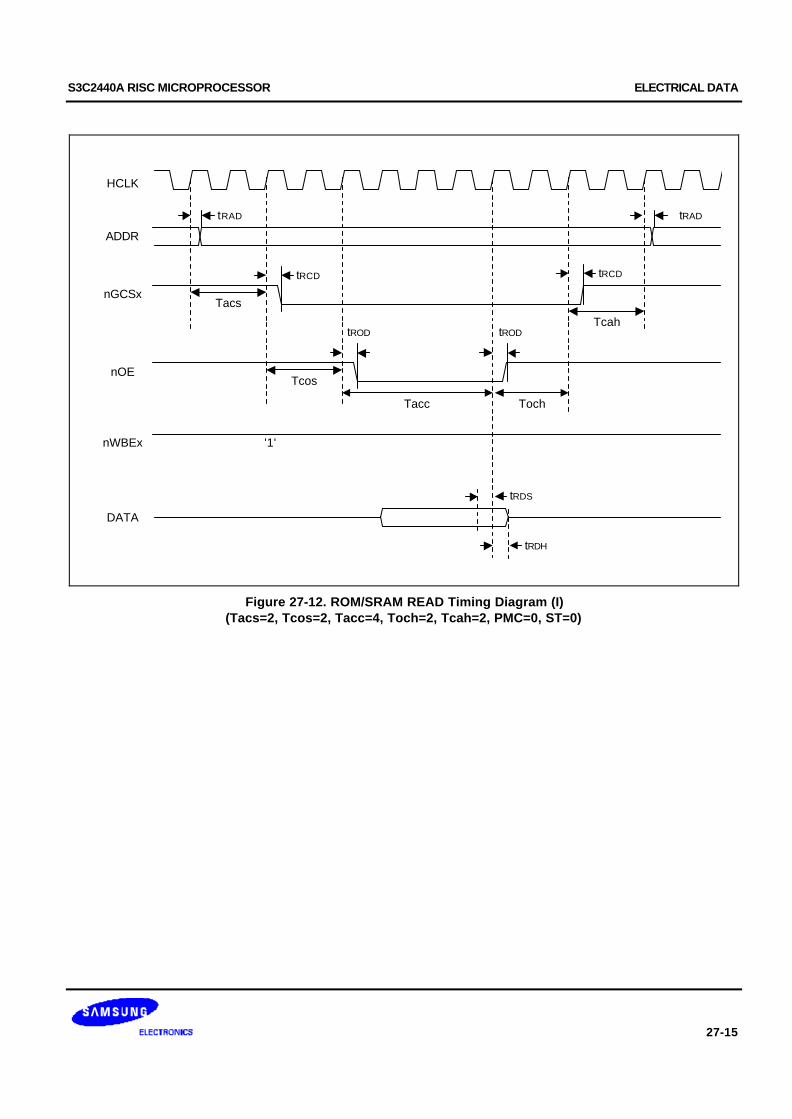
S3C2440A RISC MICROPROCESSOR ELECTRICAL DATA
27-15
HCLK
nGCSx
tRAD
Tacs
nOETcos
DATA
ADDR
nWBEx '1'
Toch
Tcah
tRCD
tROD
tRDS
tRDH
tROD
tRCD
tRAD
Tacc
Figure 27-12. ROM/SRAM READ Timing Diagram (I)(Tacs=2, Tcos=2, Tacc=4, Toch=2, Tcah=2, PMC=0, ST=0)
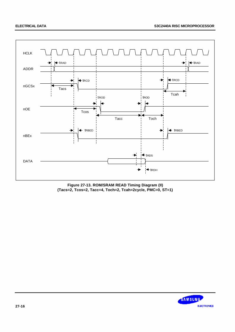
ELECTRICAL DATA S3C2440A RISC MICROPROCESSOR
27-16
HCLK
nGCSx
tRAD
Tacs
nOETcos
DATA
ADDR
nBEx
Toch
Tcah
tRCD
tROD
tRDS
tRDH
tROD
tRCD
tRAD
tRBED tRBED
Tacc
Figure 27-13. ROM/SRAM READ Timing Diagram (II)(Tacs=2, Tcos=2, Tacc=4, Toch=2, Tcah=2cycle, PMC=0, ST=1)
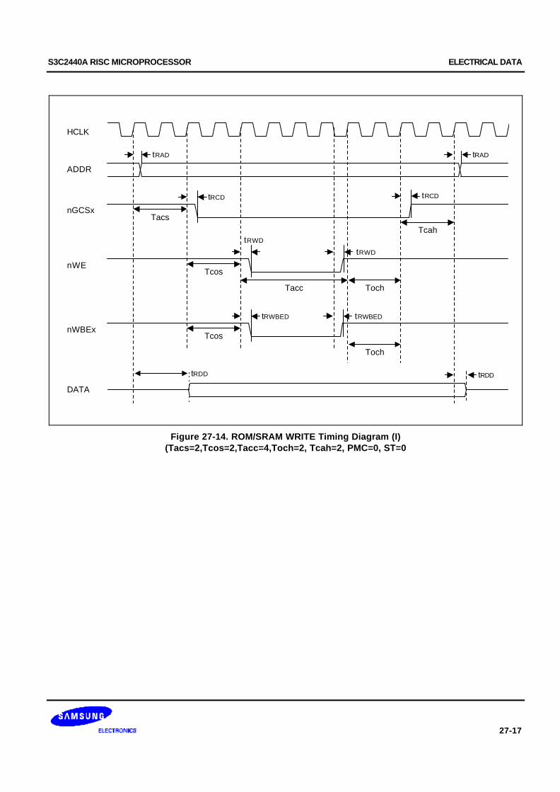
S3C2440A RISC MICROPROCESSOR ELECTRICAL DATA
27-17
HCLK
nGCSx
tRAD
Tacs
nWETcos
DATA
ADDR
nWBEx
Toch
Tcah
tRCD
tRWD
tRDD
tRWD
tRCD
tRAD
Tcos
Toch
tRWBED tRWBED
Tacc
tRDD
Figure 27-14. ROM/SRAM WRITE Timing Diagram (I)(Tacs=2,Tcos=2,Tacc=4,Toch=2, Tcah=2, PMC=0, ST=0
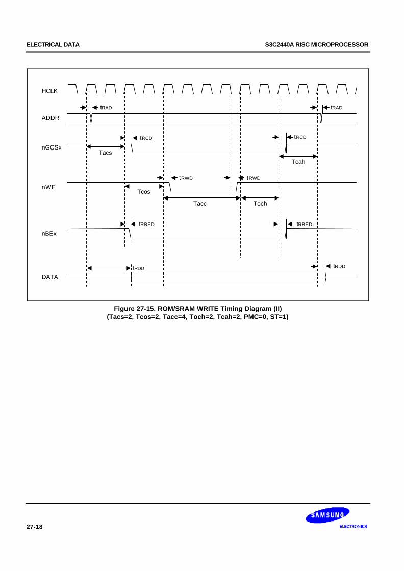
ELECTRICAL DATA S3C2440A RISC MICROPROCESSOR
27-18
HCLK
nGCSx
tRAD
Tacs
nWETcos
DATA
ADDR
nBEx
Toch
Tcah
tRCD
tRWD
tRDD
tRWD
tRCD
tRAD
tRBED tRBED
Tacc
tRDD
Figure 27-15. ROM/SRAM WRITE Timing Diagram (II)(Tacs=2, Tcos=2, Tacc=4, Toch=2, Tcah=2, PMC=0, ST=1)
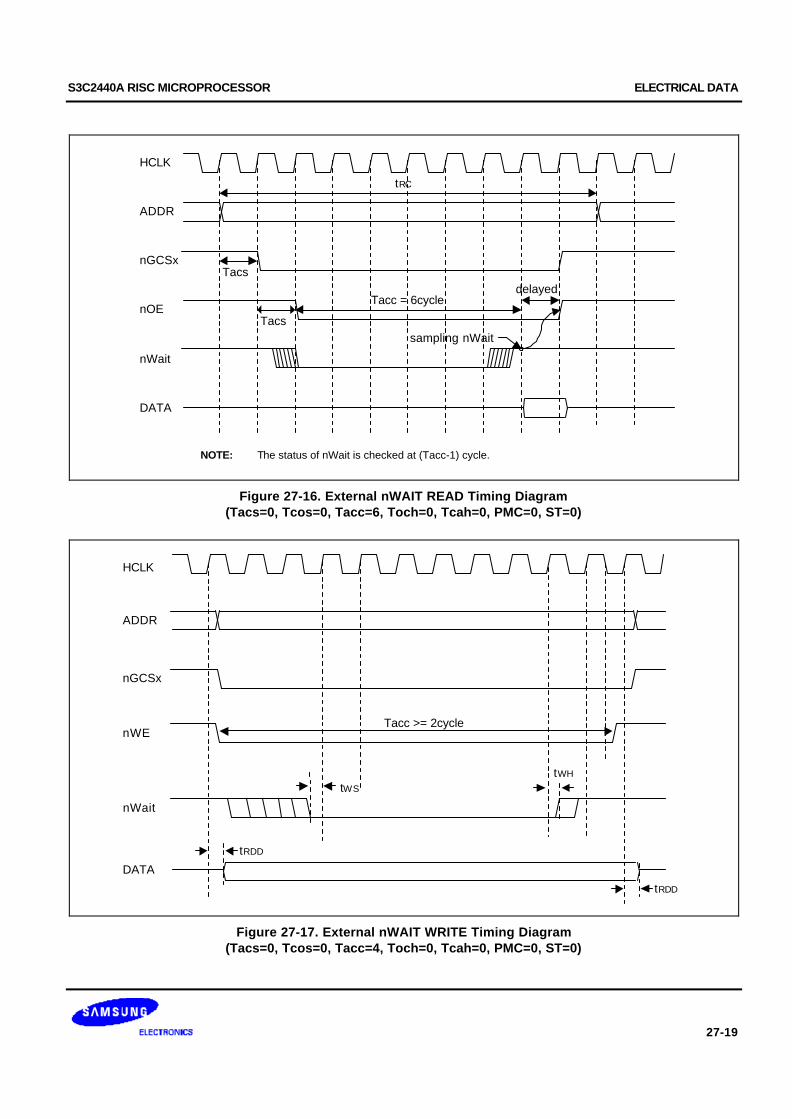
S3C2440A RISC MICROPROCESSOR ELECTRICAL DATA
27-19
HCLK
nGCSx
nOETacc = 6cycle
nWait
DATA
ADDR
Tacs
Tacs
delayed
tRC
NOTE: The status of nWait is checked at (Tacc-1) cycle.
sampling nWait
Figure 27-16. External nWAIT READ Timing Diagram(Tacs=0, Tcos=0, Tacc=6, Toch=0, Tcah=0, PMC=0, ST=0)
HCLK
nGCSx
nWE
DATA
ADDR
tRDD
tRDD
Tacc >= 2cycle
nWait
tWS
tWH
Figure 27-17. External nWAIT WRITE Timing Diagram(Tacs=0, Tcos=0, Tacc=4, Toch=0, Tcah=0, PMC=0, ST=0)
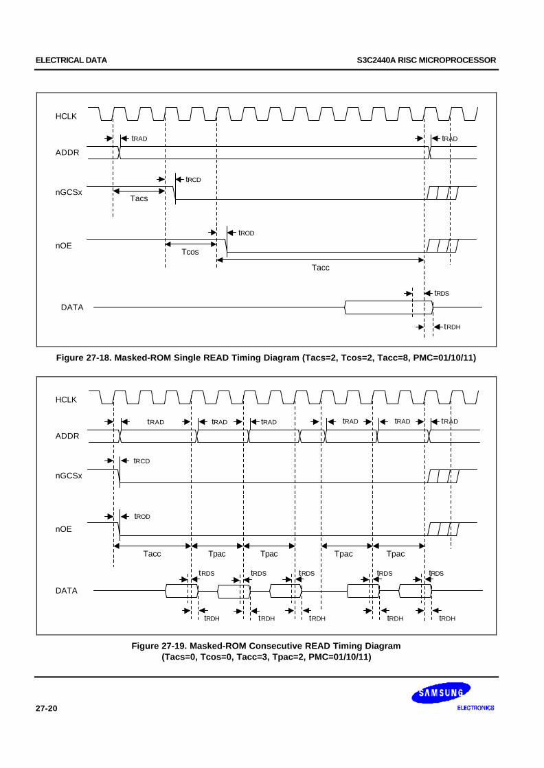
ELECTRICAL DATA S3C2440A RISC MICROPROCESSOR
27-20
HCLK
nGCSx
tRAD
Tacs
nOETcos
DATA
ADDR
tRCD
tROD
tRDS
tRDH
tRAD
Tacc
Figure 27-18. Masked-ROM Single READ Timing Diagram (Tacs=2, Tcos=2, Tacc=8, PMC=01/10/11)
HCLK
nGCSx
tRAD
nOE
DATA
ADDR
tRCD
tROD
tRDS
tRDH
tRAD
Tacc Tpac Tpac Tpac Tpac
tRAD tRAD tRAD tRAD
tRDS
tRDH
tRDS
tRDH
tRDS
tRDH
tRDS
tRDH
Figure 27-19. Masked-ROM Consecutive READ Timing Diagram(Tacs=0, Tcos=0, Tacc=3, Tpac=2, PMC=01/10/11)
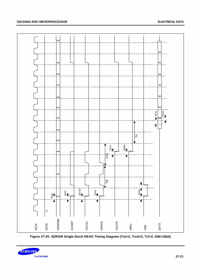
S3C2440A RISC MICROPROCESSOR ELECTRICAL DATA
27-21
SC
LK
nSR
AS
tSA
D
Trp
nSC
AS
DA
TA
AD
DR
/BA
nBE
x
tSR
D
tSD
S
tSD
H
SC
KE
A10
/AP
nGC
Sx
tSC
SD
nWE
tSA
D
tSC
D
tSW
D
'1'
Trc
d
tSB
ED
Tcl
Figure 27-20. SDRAM Single Burst READ Timing Diagram (Trp=2, Trcd=2, Tcl=2, DW=16bit)
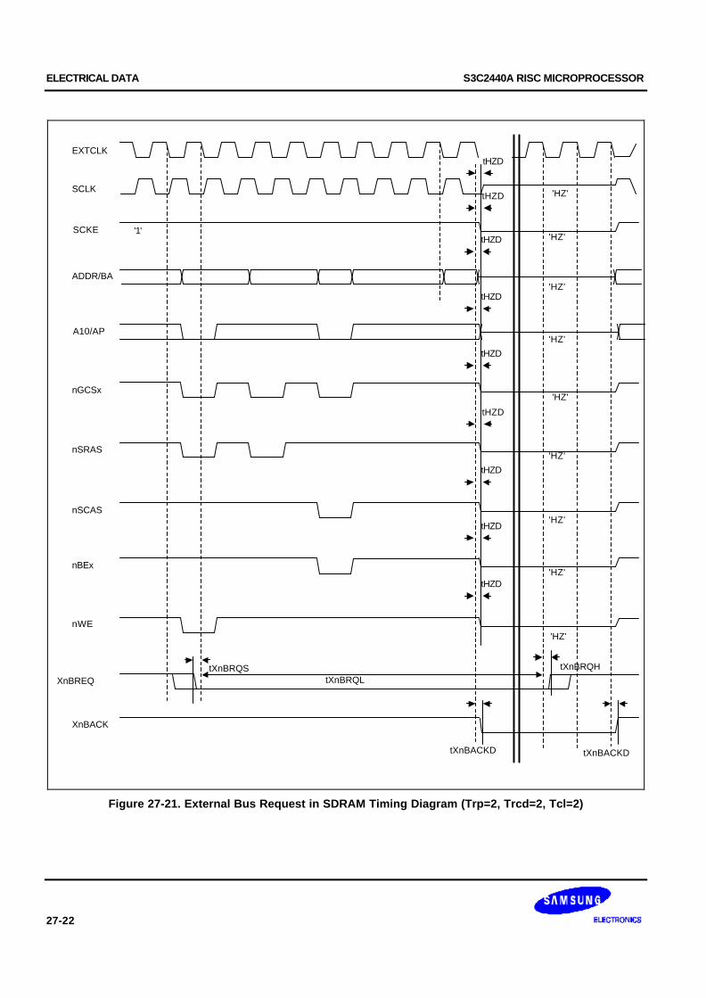
ELECTRICAL DATA S3C2440A RISC MICROPROCESSOR
27-22
SCLK
nSRAS
nSCAS
ADDR/BA
nBEx
tXnBRQHtXnBRQS
SCKE
A10/AP
nGCSx
nWE
'1'
XnBREQ
XnBACK
EXTCLK
tXnBACKD tXnBACKD
'HZ'
'HZ'
'HZ'
'HZ'
'HZ'
'HZ'
'HZ'
'HZ'
'HZ'
tHZD
tHZD
tHZD
tHZD
tHZD
tHZD
tHZD
tHZD
tHZD
tXnBRQL
Figure 27-21. External Bus Request in SDRAM Timing Diagram (Trp=2, Trcd=2, Tcl=2)
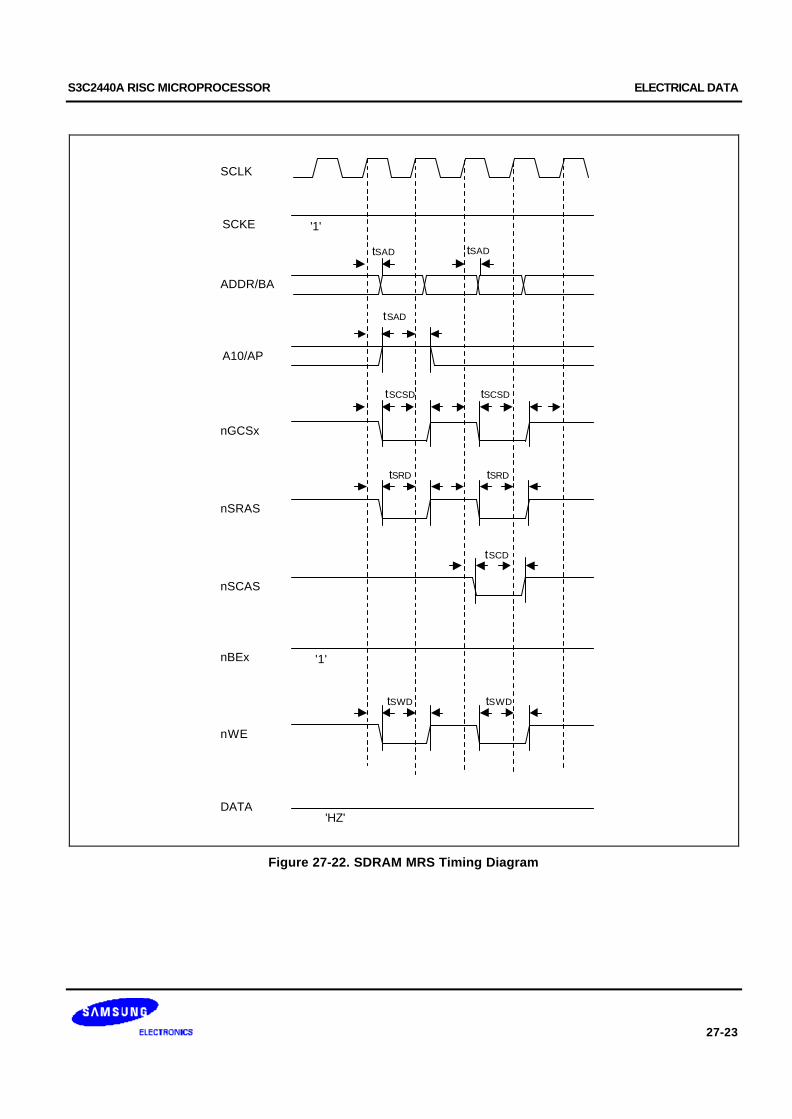
S3C2440A RISC MICROPROCESSOR ELECTRICAL DATA
27-23
SCLK
nSRAS
tSAD
nSCAS
DATA
ADDR/BA
nBEx
tSRD
SCKE
A10/AP
nGCSx
tSCSD
nWE
tSAD
tSCD
tSWD
'1'
tSAD
tSCSD
tSRD
'HZ'
'1'
tSWD
Figure 27-22. SDRAM MRS Timing Diagram
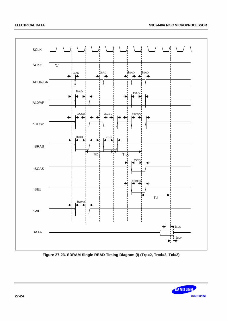
ELECTRICAL DATA S3C2440A RISC MICROPROCESSOR
27-24
SCLK
nSRAS
tSAD
Trp
nSCAS
DATA
ADDR/BA
nBEx
tSRD
tSDS
tSDH
SCKE
A10/AP
nGCSx
tSCSD
nWE
tSAD
tSCD
tSWD
'1'
tSADtSAD
Trcd
tSCSD
tSRD
tSCSD
tSAD
tSAD
tSBED
Tcl
Figure 27-23. SDRAM Single READ Timing Diagram (I) (Trp=2, Trcd=2, Tcl=2)
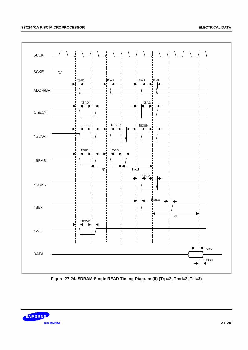
S3C2440A RISC MICROPROCESSOR ELECTRICAL DATA
27-25
SCLK
nSRAS
tSAD
Trp
nSCAS
DATA
ADDR/BA
nBEx
tSRD
tSDS
tSDH
SCKE
A10/AP
nGCSx
tSCSD
nWE
tSAD
tSCD
tSWD
'1'
tSADtSAD
Trcd
tSCSD
tSRD
tSCSD
tSAD
tSAD
tSBED
Tcl
Figure 27-24. SDRAM Single READ Timing Diagram (II) (Trp=2, Trcd=2, Tcl=3)
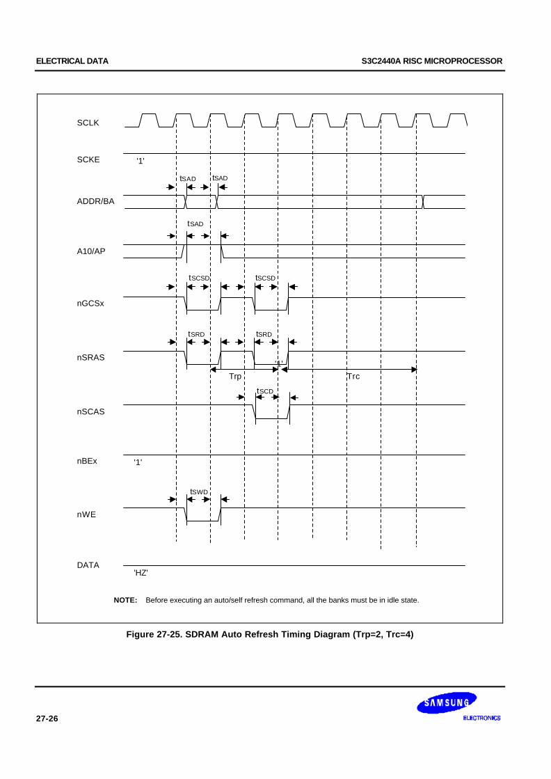
ELECTRICAL DATA S3C2440A RISC MICROPROCESSOR
27-26
SCLK
nSRAS
tSAD
Trp
nSCAS
DATA
ADDR/BA
nBEx
tSRD
SCKE
A10/AP
nGCSx
tSCSD
nWE
tSAD
tSCD
tSWD
'1'
tSAD
tSCSD
tSRD
'1'
'1'
'HZ'
Trc
NOTE: Before executing an auto/self refresh command, all the banks must be in idle state.
Figure 27-25. SDRAM Auto Refresh Timing Diagram (Trp=2, Trc=4)
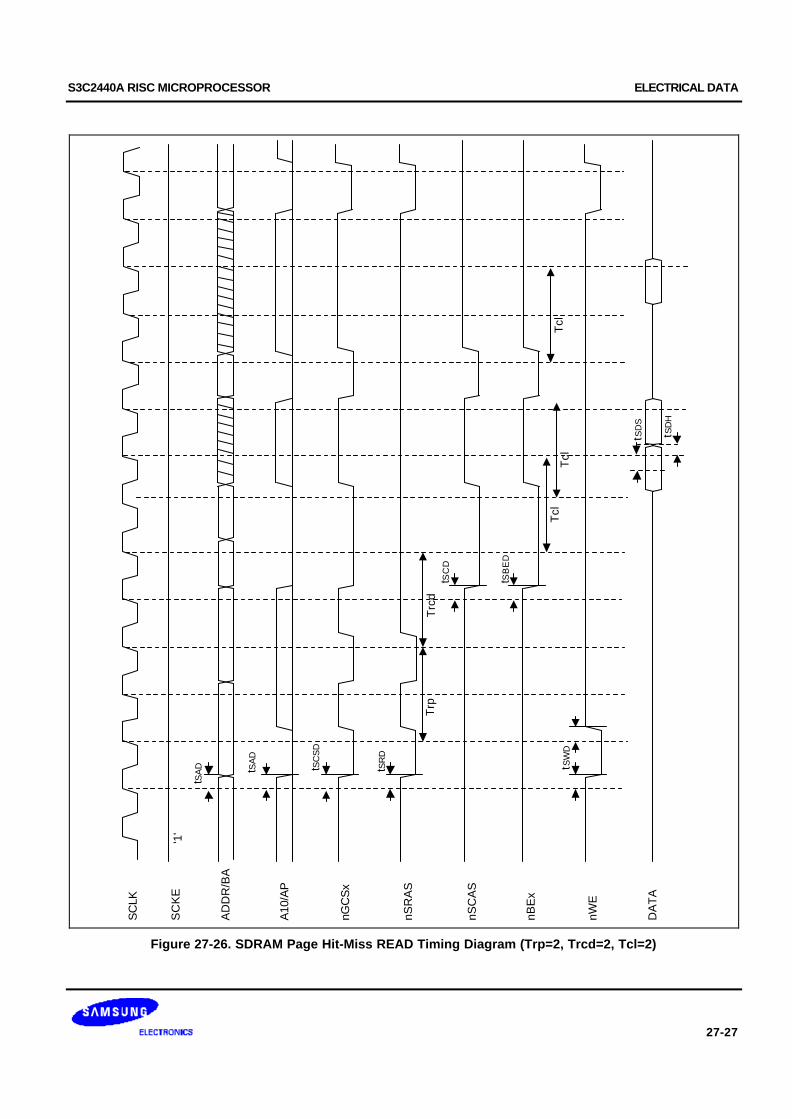
S3C2440A RISC MICROPROCESSOR ELECTRICAL DATA
27-27
SC
LK
nSR
AS
tSA
D
Trp
nSC
AS
DA
TA
AD
DR
/BA
nBE
x
tSR
D
tSD
S
tSD
H
SC
KE
A10
/AP
nGC
Sx
tSC
SD
nWE
tSA
D
tSC
D
tSW
D
'1'
Trc
d
tSB
ED
Tcl
Tcl
Tcl
Figure 27-26. SDRAM Page Hit-Miss READ Timing Diagram (Trp=2, Trcd=2, Tcl=2)
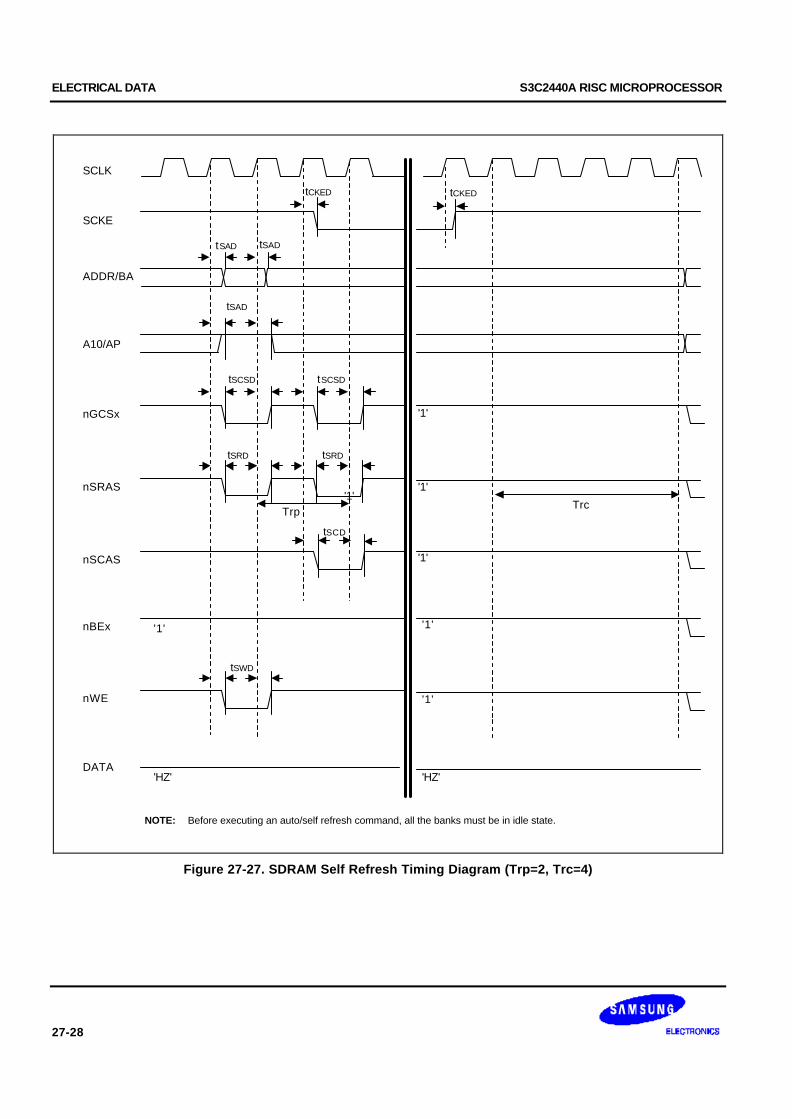
ELECTRICAL DATA S3C2440A RISC MICROPROCESSOR
27-28
SCLK
nSRAS
tSAD
Trp
nSCAS
DATA
ADDR/BA
nBEx
tSRD
SCKE
A10/AP
nGCSx
tSCSD
nWE
tSAD
tSCD
tSWD
tSAD
tSCSD
tSRD
'1'
'1'
'HZ'
Trc
tCKED
'HZ'
'1'
'1'
'1'
'1'
'1'
tCKED
NOTE: Before executing an auto/self refresh command, all the banks must be in idle state.
Figure 27-27. SDRAM Self Refresh Timing Diagram (Trp=2, Trc=4)

S3C2440A RISC MICROPROCESSOR ELECTRICAL DATA
27-29
SCLK
nSRAS
tSAD
Trp
nSCAS
DATA
ADDR/BA
nBEx
tSRD
tSDD
tSDD
SCKE
A10/AP
nGCSx
tSCSD
nWE
tSAD
tSCD
tSWD
'1'
tSADtSAD
Trcd
tSCSD
tSRD
tSCSD
tSAD
tSAD
tSBED
tSWD
Figure 27-28. SDRAM Single Write Timing Diagram (Trp=2, Trcd=2)

ELECTRICAL DATA S3C2440A RISC MICROPROCESSOR
27-30
SC
LK
nSR
AS
tSA
D
Trp
nSC
AS
DA
TA
AD
DR
/BA
nBE
x
tSR
D
tSD
D
tSD
D
SC
KE
A10
/AP
nGC
Sx
tSC
SD
nWE
tSA
D
tSC
D
tSW
D
'1'
Trc
d
tSB
ED
Figure 27-29. SDRAM Page Hit-Miss Write Timing Diagram (Trp=2, Trcd=2, Tcl=2)
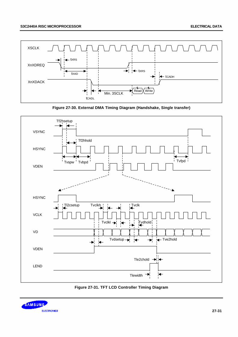
S3C2440A RISC MICROPROCESSOR ELECTRICAL DATA
27-31
XSCLK
tXRS
tXRS
tCADL
tCADHtXAD
XnXDREQ
XnXDACK
Read WriteMin. 3SCLK
Figure 27-30. External DMA Timing Diagram (Handshake, Single transfer)
VSYNC
HSYNC
VDEN
Tf2hsetup
Tf2hhold
Tvspw Tvbpd Tvfpd
HSYNC
VCLK
VD
VDEN
LEND
Tl2csetup Tvclkh Tvclk
Tvclkl Tvdhold
Tvdsetup Tve2hold
Tle2chold
Tlewidth
Figure 27-31. TFT LCD Controller Timing Diagram
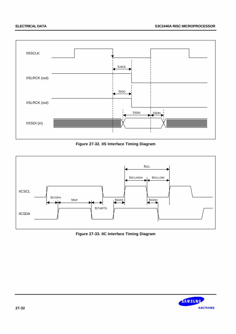
ELECTRICAL DATA S3C2440A RISC MICROPROCESSOR
27-32
IISSCLK
tLRCK
IISLRCK (out)
tSDO
IISLRCK (out)
tSDIHtSDIS
IISSDI (in)
Figure 27-32. IIS Interface Timing Diagram
tSTOPH
tSTARTS
tSDAS tSDAHtBUF
tSCLHIGH tSCLLOW
fSCL
IICSCL
IICSDA
Figure 27-33. IIC Interface Timing Diagram
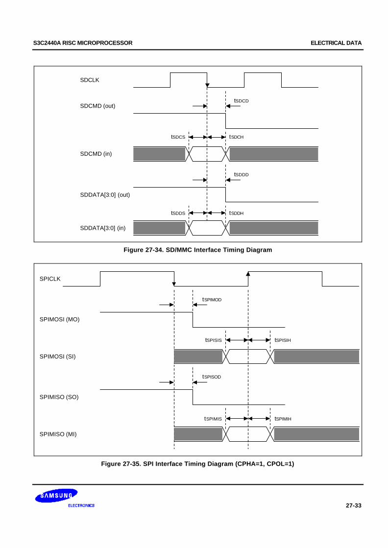
S3C2440A RISC MICROPROCESSOR ELECTRICAL DATA
27-33
SDCLK
tSDCDSDCMD (out)
tSDCHtSDCS
tSDDD
SDCMD (in)
tSDDHtSDDS
SDDATA[3:0] (in)
SDDATA[3:0] (out)
Figure 27-34. SD/MMC Interface Timing Diagram
SPICLK
tSPIMOD
tSPISIHtSPISIS
tSPISOD
tSPIMIHtSPIMIS
SPIMOSI (MO)
SPIMOSI (SI)
SPIMISO (SO)
SPIMISO (MI)
Figure 27-35. SPI Interface Timing Diagram (CPHA=1, CPOL=1)
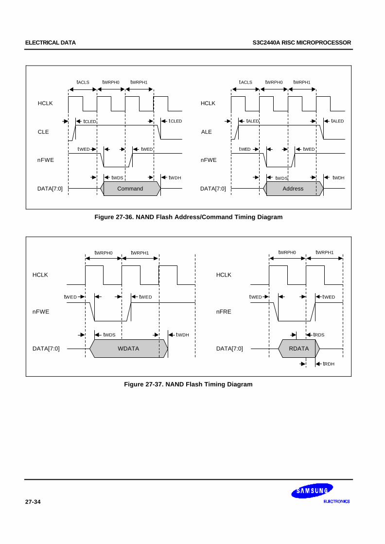
ELECTRICAL DATA S3C2440A RISC MICROPROCESSOR
27-34
tACLS tWRPH0 tWRPH1
Command
tWRPH0 tWRPH1
Address
HCLK
ALE
nFWE
DATA[7:0] DATA[7:0]
HCLK
CLE
nFWE
tCLED tCLED
tWED tWED
tWDS tWDH
tALED
tWED
tWDS
tALED
tWED
tWDH
tACLS
Figure 27-36. NAND Flash Address/Command Timing Diagram
HCLK
nFWE
tWRPH0 tWRPH1
DATA[7:0]
HCLK
nFRE
tWRPH0 tWRPH1
DATA[7:0]
tWEDtWED
tWDH
tWEDtWED
tRDS
tRDH
tWDS
WDATA RDATA
Figure 27-37. NAND Flash Timing Diagram
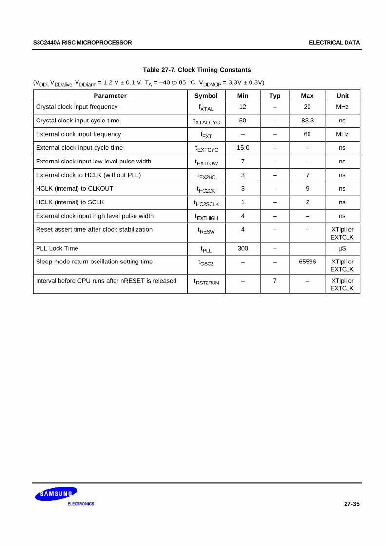
S3C2440A RISC MICROPROCESSOR ELECTRICAL DATA
27-35
Table 27-7. Clock Timing Constants
(VDDi, VDDalive, VDDiarm = 1.2 V ± 0.1 V, TA = –40 to 85 °C, VDDMOP = 3.3V ± 0.3V)
Parameter Symbol Min Typ Max Unit
Crystal clock input frequency fXTAL 12 – 20 MHz
Crystal clock input cycle time tXTALCYC 50 – 83.3 ns
External clock input frequency fEXT – – 66 MHz
External clock input cycle time tEXTCYC 15.0 – – ns
External clock input low level pulse width tEXTLOW 7 – – ns
External clock to HCLK (without PLL) tEX2HC 3 – 7 ns
HCLK (internal) to CLKOUT tHC2CK 3 – 9 ns
HCLK (internal) to SCLK tHC2SCLK 1 – 2 ns
External clock input high level pulse width tEXTHIGH 4 – – ns
Reset assert time after clock stabilization tRESW 4 – – XTIpll orEXTCLK
PLL Lock Time tPLL 300 – µS
Sleep mode return oscillation setting time tOSC2 – – 65536 XTIpll orEXTCLK
Interval before CPU runs after nRESET is released tRST2RUN – 7 – XTIpll orEXTCLK
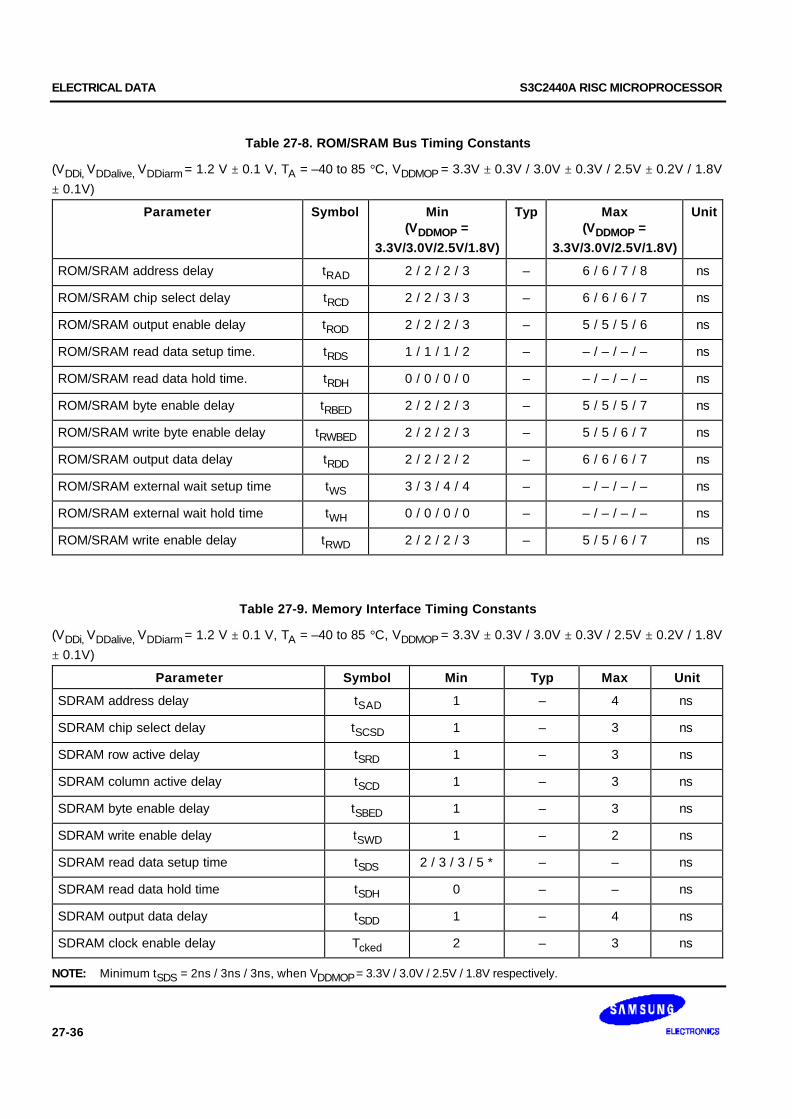
ELECTRICAL DATA S3C2440A RISC MICROPROCESSOR
27-36
Table 27-8. ROM/SRAM Bus Timing Constants
(VDDi, VDDalive, VDDiarm = 1.2 V ± 0.1 V, TA = –40 to 85 °C, VDDMOP = 3.3V ± 0.3V / 3.0V ± 0.3V / 2.5V ± 0.2V / 1.8V
± 0.1V)
Parameter Symbol Min(VDDMOP =
3.3V/3.0V/2.5V/1.8V)
Typ Max(VDDMOP =
3.3V/3.0V/2.5V/1.8V)
Unit
ROM/SRAM address delay tRAD 2 / 2 / 2 / 3 – 6 / 6 / 7 / 8 ns
ROM/SRAM chip select delay tRCD 2 / 2 / 3 / 3 – 6 / 6 / 6 / 7 ns
ROM/SRAM output enable delay tROD 2 / 2 / 2 / 3 – 5 / 5 / 5 / 6 ns
ROM/SRAM read data setup time. tRDS 1 / 1 / 1 / 2 – – / – / – / – ns
ROM/SRAM read data hold time. tRDH 0 / 0 / 0 / 0 – – / – / – / – ns
ROM/SRAM byte enable delay tRBED 2 / 2 / 2 / 3 – 5 / 5 / 5 / 7 ns
ROM/SRAM write byte enable delay tRWBED 2 / 2 / 2 / 3 – 5 / 5 / 6 / 7 ns
ROM/SRAM output data delay tRDD 2 / 2 / 2 / 2 – 6 / 6 / 6 / 7 ns
ROM/SRAM external wait setup time tWS 3 / 3 / 4 / 4 – – / – / – / – ns
ROM/SRAM external wait hold time tWH 0 / 0 / 0 / 0 – – / – / – / – ns
ROM/SRAM write enable delay tRWD 2 / 2 / 2 / 3 – 5 / 5 / 6 / 7 ns
Table 27-9. Memory Interface Timing Constants
(VDDi, VDDalive, VDDiarm = 1.2 V ± 0.1 V, TA = –40 to 85 °C, VDDMOP = 3.3V ± 0.3V / 3.0V ± 0.3V / 2.5V ± 0.2V / 1.8V
± 0.1V)
Parameter Symbol Min Typ Max Unit
SDRAM address delay tSAD 1 – 4 ns
SDRAM chip select delay tSCSD 1 – 3 ns
SDRAM row active delay tSRD 1 – 3 ns
SDRAM column active delay tSCD 1 – 3 ns
SDRAM byte enable delay tSBED 1 – 3 ns
SDRAM write enable delay tSWD 1 – 2 ns
SDRAM read data setup time tSDS 2 / 3 / 3 / 5 * – – ns
SDRAM read data hold time tSDH 0 – – ns
SDRAM output data delay tSDD 1 – 4 ns
SDRAM clock enable delay Tcked 2 – 3 ns
NOTE: Minimum tSDS = 2ns / 3ns / 3ns, when VDDMOP = 3.3V / 3.0V / 2.5V / 1.8V respectively.
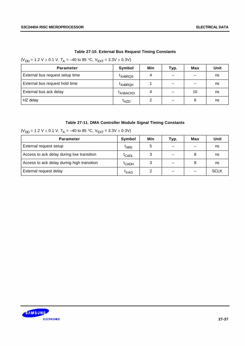
S3C2440A RISC MICROPROCESSOR ELECTRICAL DATA
27-37
Table 27-10. External Bus Request Timing Constants
(VDD = 1.2 V ± 0.1 V, TA = –40 to 85 °C, VEXT = 3.3V ± 0.3V)
Parameter Symbol Min Typ. Max Unit
External bus request setup time tXnBRQS 4 – – ns
External bus request hold time tXnBRQH 1 – – ns
External bus ack delay tXnBACKD 4 – 10 ns
HZ delay tHZD 2 – 6 ns
Table 27-11. DMA Controller Module Signal Timing Constants
(VDD = 1.2 V ± 0.1 V, TA = –40 to 85 °C, VEXT = 3.3V ± 0.3V)
Parameter Symbol Min Typ. Max Unit
External request setup tXRS 5 – – ns
Access to ack delay during low transition tCADL 3 – 8 ns
Access to ack delay during high transition tCADH 3 – 8 ns
External request delay tXAD 2 – – SCLK

ELECTRICAL DATA S3C2440A RISC MICROPROCESSOR
27-38
Table 27-12. TFT LCD Controller Module Signal Timing Constants
(VDD = 1.2 V ± 0.05 V, TA = –40 to 85 °C, VEXT = 3.3V ± 0.3V)
Parameter Symbol Min Typ Max Units
Vertical sync pulse width Tvspw VSPW + 1 – – Phclk (1)
Vertical back porch delay Tvbpd VBPD+1 – – Phclk
Vertical front porch delay Tvfpd VFPD+1 – – Phclk
VCLK pulse width Tvclk 1 – – Pvclk (2)
VCLK pulse width high Tvclkh 0.5 – – Pvclk
VCLK pulse width low Tvclkl 0.5 – – Pvclk
Hsync setup to VCLK falling edge Tl2csetup 0.5 – – Pvclk
VDEN setup to VCLK falling edge Tde2csetup 0.5 – – Pvclk
VDEN hold from VCLK falling edge Tde2chold 0.5 – – Pvclk
VD setup to VCLK falling edge Tvd2csetup 0.5 – – Pvclk
VD hold from VCLK falling edge Tvd2chold 0.5 – – Pvclk
VSYNC setup to HSYNC falling edge Tf2hsetup HSPW + 1 – – Pvclk
VSYNC hold from HSYNC falling edge Tf2hhold HBPD + HFPD +HOZVAL + 3
– – Pvclk
NOTES:1. HSYNC period2. VCLK period
Table 27-13. IIS Controller Module Signal Timing Constants
(VDD = 1.2 V ± 0.1 V, TA = –40 to 85 °C, VEXT = 3.3V ± 0.3V)
Parameter Symbol Min Typ. Max Unit
IISLRCK delay time tLRCK 0 – 3 ns
IISDO delay time tSDO 1 – 2 ns
IISDI input setup time tSDIS 13 – – ns
IISDI input hold time tSDIH 1 – – ns
CODEC clock frequency fCODEC 1/16 – 1 fIIS_BLOCK
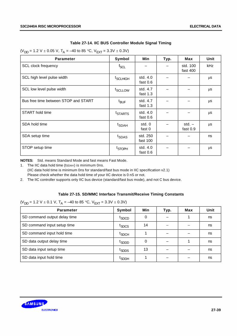
S3C2440A RISC MICROPROCESSOR ELECTRICAL DATA
27-39
Table 27-14. IIC BUS Controller Module Signal Timing
(VDD = 1.2 V ± 0.05 V, TA = –40 to 85 °C, VEXT = 3.3V ± 0.3V)
Parameter Symbol Min Typ. Max Unit
SCL clock frequency fSCL – – std. 100fast 400
kHz
SCL high level pulse width tSCLHIGH std. 4.0fast 0.6
– – µs
SCL low level pulse width tSCLLOW std. 4.7fast 1.3
– – µs
Bus free time between STOP and START tBUF std. 4.7fast 1.3
– – µs
START hold time tSTARTS std. 4.0fast 0.6
– – µs
SDA hold time tSDAH std. 0fast 0
– std. –fast 0.9
µs
SDA setup time tSDAS std. 250fast 100
– – ns
STOP setup time tSTOPH std. 4.0fast 0.6
– – µs
NOTES: Std. means Standard Mode and fast means Fast Mode.1. The IIC data hold time (tSDAH) is minimum 0ns.
(IIC data hold time is minimum 0ns for standard/fast bus mode in IIC specification v2.1)Please check whether the data hold time of your IIC device is 0 nS or not.
2. The IIC controller supports only IIC bus device (standard/fast bus mode), and not C bus device.
Table 27-15. SD/MMC Interface Transmit/Receive Timing Constants
(VDD = 1.2 V ± 0.1 V, TA = –40 to 85 °C, VEXT = 3.3V ± 0.3V)
Parameter Symbol Min Typ. Max Unit
SD command output delay time tSDCD 0 – 1 ns
SD command input setup time tSDCS 14 – – ns
SD command input hold time tSDCH 1 – – ns
SD data output delay time tSDDD 0 – 1 ns
SD data input setup time tSDDS 13 – – ns
SD data input hold time tSDDH 1 – – ns
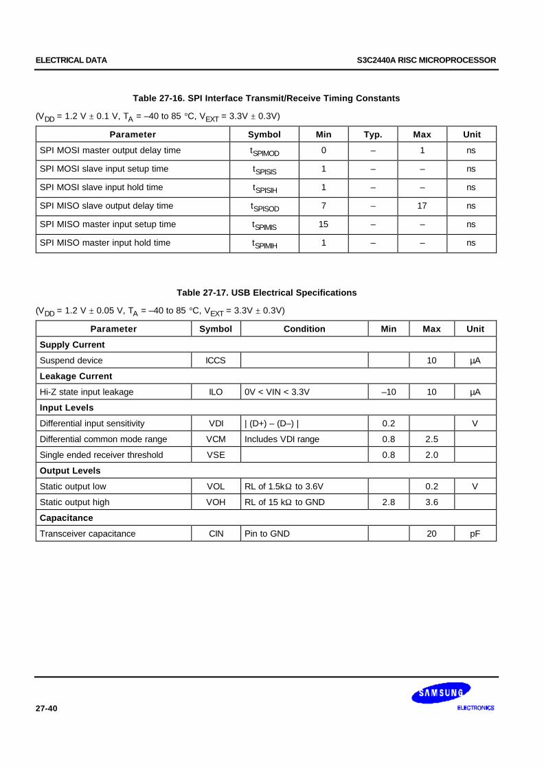
ELECTRICAL DATA S3C2440A RISC MICROPROCESSOR
27-40
Table 27-16. SPI Interface Transmit/Receive Timing Constants
(VDD = 1.2 V ± 0.1 V, TA = –40 to 85 °C, VEXT = 3.3V ± 0.3V)
Parameter Symbol Min Typ. Max Unit
SPI MOSI master output delay time tSPIMOD 0 – 1 ns
SPI MOSI slave input setup time tSPISIS 1 – – ns
SPI MOSI slave input hold time tSPISIH 1 – – ns
SPI MISO slave output delay time tSPISOD 7 – 17 ns
SPI MISO master input setup time tSPIMIS 15 – – ns
SPI MISO master input hold time tSPIMIH 1 – – ns
Table 27-17. USB Electrical Specifications
(VDD = 1.2 V ± 0.05 V, TA = –40 to 85 °C, VEXT = 3.3V ± 0.3V)
Parameter Symbol Condition Min Max Unit
Supply Current
Suspend device ICCS 10 µA
Leakage Current
Hi-Z state input leakage ILO 0V < VIN < 3.3V –10 10 µA
Input Levels
Differential input sensitivity VDI | (D+) – (D–) | 0.2 V
Differential common mode range VCM Includes VDI range 0.8 2.5
Single ended receiver threshold VSE 0.8 2.0
Output Levels
Static output low VOL RL of 1.5kΩ to 3.6V 0.2 V
Static output high VOH RL of 15 kΩ to GND 2.8 3.6
Capacitance
Transceiver capacitance CIN Pin to GND 20 pF
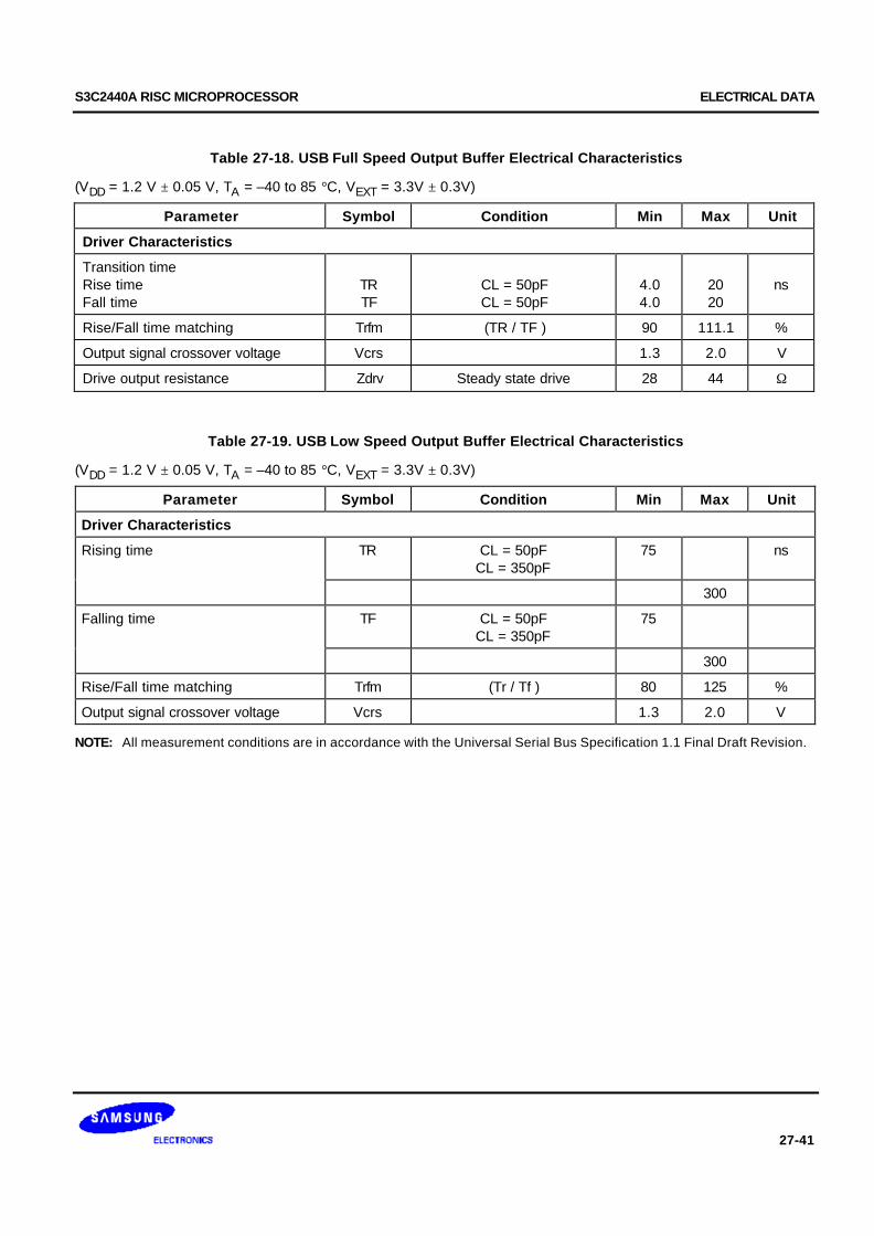
S3C2440A RISC MICROPROCESSOR ELECTRICAL DATA
27-41
Table 27-18. USB Full Speed Output Buffer Electrical Characteristics
(VDD = 1.2 V ± 0.05 V, TA = –40 to 85 °C, VEXT = 3.3V ± 0.3V)
Parameter Symbol Condition Min Max Unit
Driver Characteristics
Transition timeRise timeFall time
TRTF
CL = 50pFCL = 50pF
4.04.0
2020
ns
Rise/Fall time matching Trfm (TR / TF ) 90 111.1 %
Output signal crossover voltage Vcrs 1.3 2.0 V
Drive output resistance Zdrv Steady state drive 28 44 Ω
Table 27-19. USB Low Speed Output Buffer Electrical Characteristics
(VDD = 1.2 V ± 0.05 V, TA = –40 to 85 °C, VEXT = 3.3V ± 0.3V)
Parameter Symbol Condition Min Max Unit
Driver Characteristics
Rising time TR CL = 50pFCL = 350pF
75 ns
300
Falling time TF CL = 50pFCL = 350pF
75
300
Rise/Fall time matching Trfm (Tr / Tf ) 80 125 %
Output signal crossover voltage Vcrs 1.3 2.0 V
NOTE: All measurement conditions are in accordance with the Universal Serial Bus Specification 1.1 Final Draft Revision.
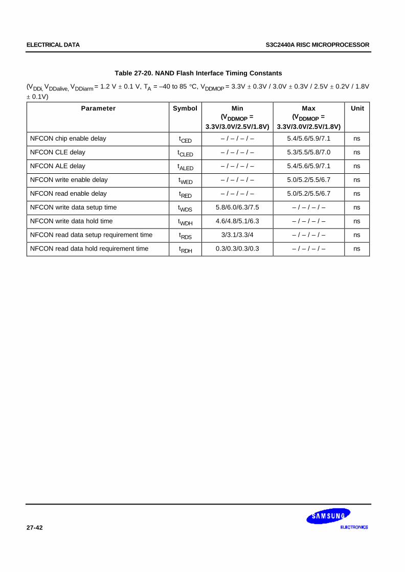
ELECTRICAL DATA S3C2440A RISC MICROPROCESSOR
27-42
Table 27-20. NAND Flash Interface Timing Constants
(VDDi, VDDalive, VDDiarm = 1.2 V ± 0.1 V, TA = –40 to 85 °C, VDDMOP = 3.3V ± 0.3V / 3.0V ± 0.3V / 2.5V ± 0.2V / 1.8V
± 0.1V)
Parameter Symbol Min(VDDMOP =
3.3V/3.0V/2.5V/1.8V)
Max(VDDMOP =
3.3V/3.0V/2.5V/1.8V)
Unit
NFCON chip enable delay tCED – / – / – / – 5.4/5.6/5.9/7.1 ns
NFCON CLE delay tCLED – / – / – / – 5.3/5.5/5.8/7.0 ns
NFCON ALE delay tALED – / – / – / – 5.4/5.6/5.9/7.1 ns
NFCON write enable delay tWED – / – / – / – 5.0/5.2/5.5/6.7 ns
NFCON read enable delay tRED – / – / – / – 5.0/5.2/5.5/6.7 ns
NFCON write data setup time tWDS 5.8/6.0/6.3/7.5 – / – / – / – ns
NFCON write data hold time tWDH 4.6/4.8/5.1/6.3 – / – / – / – ns
NFCON read data setup requirement time tRDS 3/3.1/3.3/4 – / – / – / – ns
NFCON read data hold requirement time tRDH 0.3/0.3/0.3/0.3 – / – / – / – ns
This datasheet has been downloaded from:
www.DatasheetCatalog.com
Datasheets for electronic components.