S Series Data Sheet - Bel - Power | Protect | Connect Series Data Sheet 100 Watt DC-DC and AC-DC...
31
S Series Data Sheet 100 Watt DC-DC and AC-DC Converters BCD20004-G Rev AE, 24-May-2017 Page 1 of 31 MELCHER The Power Partners. Table of Contents Page Page Description The S Series of DC-DC and AC-DC converters represents a broad and flexible range of power supplies for use in advanced electronic systems. Features include high efficiency, high reliability, low output voltage noise and excellent dynamic response to load/line changes. LS models can be powered by DC or AC with a wide-input frequency range (without PFC). The converter inputs are protected against surges and transients. An input over- and undervoltage lockout circuitry disables the outputs, if the input voltage is outside of the specified range. Certain types include an inrush current limiter preventing circuit breakers and fuses from tripping at switch- on. All outputs are open- and short-circuit proof, and are protected against overvoltages by means of built-in suppressor diodes. The output can be inhibited by a logic signal applied to pin 18 (i). If the inhibit function is not used, pin 18 must be connected with pin 14 to enable the outputs. LED indicators display the status of the converter and allow for visual monitoring of the system at any time. Features • RoHS lead-free-solder and lead-solder-exempted products are available. • Compliant to EN 50155, EN 50121-3-2. • Compliant to EN 45545 (version V108 or later) • Class I equipment • Extremely wide input voltage ranges from 8 to 385 VDC, and 85 to 264 VAC, 47 to 440 Hz • Input over- and undervoltage lockout • Adjustable output voltage with remote on/off • 1 or 2 outputs: SELV, no load, overload, and short- circuit proof • Rectangular current limiting characteristic • PCBs protected by lacquer • Very high reliability Safety-approved to the latest edition of IEC/EN 60950-1 and UL/CSA 60950-1. Full input-to-output, input-to-case, output-to-case, and output to output isolation is provided. The converters are designed, built, and safety-approved to the international safety standards IEC/EN 60950-1. They observe EN 50155 and EN 50121-3-2 and are particularly suitable for railway applications. The case design allows operation at nominal load up to 71 °C in a free-air ambient temperature. If forced cooling is provided, the ambient temperature may exceed 71 °C, but the case temperature must remain below 95 °C under all conditions. A temperature sensor generates an inhibit signal, which disables the outputs when the case temperature T C exceeds the limit. The outputs are automatically re-enabled, when the temperature drops below the limit. Various options are available to adapt the converters to individual applications. The converters may either be plugged into a 19" DIN-rack system according to IEC 60297-3, or mounted to a chassis. Important: For applications requiring compliance with IEC/EN 61000-3-2 (harmonic distortion), please use our LS4000 or LS5000 Series with incorporated power factor correction (PFC). 168 6.6" 60 2.4" 12 TE 111 4.4" 3 U Description .......................................................................... 1 Model Selection .................................................................. 2 Functional Description ........................................................ 4 Electrical Input Data ............................................................ 5 Electrical Output Data ......................................................... 8 Auxiliary Functions ............................................................ 12 Electromagnetic Compatibility (EMC) ............................... 15 Immunity to Environmental Conditions ............................. 17 Mechanical Data ............................................................... 18 Safety and Installation Instructions ................................... 20 Description of Options ...................................................... 23 Accessories ....................................................................... 30 Copyright © 2017, Bel Power Solutions Inc. All rights reserved.
Transcript of S Series Data Sheet - Bel - Power | Protect | Connect Series Data Sheet 100 Watt DC-DC and AC-DC...
S Series Data Sheet100 Watt DC-DC and AC-DC Converters
BCD20004-G Rev AE, 24-May-2017 Page 1 of 31MELCHERThe Power Partners.
Table of Contents Page Page
DescriptionThe S Series of DC-DC and AC-DC converters represents abroad and flexible range of power supplies for use in advancedelectronic systems. Features include high efficiency, highreliability, low output voltage noise and excellent dynamicresponse to load/line changes. LS models can be powered byDC or AC with a wide-input frequency range (without PFC).
The converter inputs are protected against surges andtransients. An input over- and undervoltage lockout circuitrydisables the outputs, if the input voltage is outside of thespecified range. Certain types include an inrush current limiterpreventing circuit breakers and fuses from tripping at switch-on.
All outputs are open- and short-circuit proof, and are protectedagainst overvoltages by means of built-in suppressor diodes.The output can be inhibited by a logic signal applied to pin 18(i). If the inhibit function is not used, pin 18 must be connectedwith pin 14 to enable the outputs.
LED indicators display the status of the converter and allowfor visual monitoring of the system at any time.
Features
• RoHS lead-free-solder and lead-solder-exemptedproducts are available.
• Compliant to EN 50155, EN 50121-3-2.• Compliant to EN 45545 (version V108 or later)• Class I equipment• Extremely wide input voltage ranges from 8 to 385 VDC,
and 85 to 264 VAC, 47 to 440 Hz• Input over- and undervoltage lockout• Adjustable output voltage with remote on/off• 1 or 2 outputs: SELV, no load, overload, and short-
circuit proof• Rectangular current limiting characteristic• PCBs protected by lacquer• Very high reliability
Safety-approved to the latest edition of IEC/EN 60950-1and UL/CSA 60950-1.
Full input-to-output, input-to-case, output-to-case, and outputto output isolation is provided. The converters are designed,built, and safety-approved to the international safety standardsIEC/EN 60950-1. They observe EN 50155 and EN 50121-3-2and are particularly suitable for railway applications.
The case design allows operation at nominal load up to 71 °Cin a free-air ambient temperature. If forced cooling is provided,the ambient temperature may exceed 71 °C, but the casetemperature must remain below 95 °C under all conditions.
A temperature sensor generates an inhibit signal, whichdisables the outputs when the case temperature TC exceedsthe limit. The outputs are automatically re-enabled, when thetemperature drops below the limit.
Various options are available to adapt the converters toindividual applications.
The converters may either be plugged into a 19" DIN-racksystem according to IEC 60297-3, or mounted to a chassis.
Important: For applications requiring compliance with IEC/EN61000-3-2 (harmonic distortion), please use our LS4000 or LS5000Series with incorporated power factor correction (PFC).
1686.6"
602.4"12 TE
1114.4"3 U
Description .......................................................................... 1Model Selection .................................................................. 2Functional Description ........................................................ 4Electrical Input Data ............................................................ 5Electrical Output Data ......................................................... 8Auxiliary Functions ............................................................ 12
Electromagnetic Compatibility (EMC) ............................... 15Immunity to Environmental Conditions ............................. 17Mechanical Data ............................................................... 18Safety and Installation Instructions ................................... 20Description of Options ...................................................... 23Accessories ....................................................................... 30
Copyright © 2017, Bel Power Solutions Inc. All rights reserved.
S Series Data Sheet100 Watt DC-DC and AC-DC Converters
BCD20004-G Rev AE, 24-May-2017 Page 2 of 31MELCHERThe Power Partners.
Model SelectionNon-standard input/output configurations or special customer adaptations are available on request.
Table 1a: Models AS
Output 1 Output 2 Input Voltage Effic.1 Input Voltage Effic.1 Options 4
Vo nom Io nom Vo nom Io nom Vi min – Vi max ηηηηηmin Vi min – Vi max ηηηηηmin
[VDC] [A] [VDC] [A] 8 – 35 VDC [%] 14 – 70 VDC [%]
5.1 16 – – AS1001-9RG 76 BS1001-9RG 77 -7, P, D, V 2, T, B, B1, non-G
12 8 – – AS1301-9RG 81 BS1301-9RG 83 -7, P, D, T, B, B1, non-G15 6.5 – – AS1501-9RG 83 BS1501-9RG 85 24 4.2 – – AS1601-9RG 84 BS1601-9RG 86
12 4 12 3 4 AS2320-9RG 79 BS2320-9RG 80 -7, P, D, T, B, B1, non-G15 3.2 15 3 3.2 AS2540-9RG 80 BS2540-9RG 82 24 2 24 3 2 AS2660-9RG 80 BS2660-9RG 82
Table 1b: Models BS, FS, CS
Output 1 Output 2 Input Voltage Effic.1 Input Voltage Effic.1 Options 4
Vo nom Io nom Vo nom Io nom Vi min – Vi max ηηηηηmin Vi min – Vi max ηηηηηmin
[VDC] [A] [VDC] [A] 20 – 100 VDC [%] 28 – 140 VDC [%]
5.1 16 – – FS1001-9ERG 77 CS1001-9ERG 77 -7, P, D, V 2, T, B, B1, non-G
12 8 – – FS1301-9ERG 83 CS1301-9ERG 83 -7, P, D, T, B, B1, non-G15 6.5 – – FS1501-9ERG 84 CS1501-9ERG 8424 4.2 – – FS1601-9ERG 86 CS1601-9ERG 85
12 4 12 3 4 FS2320-9ERG 80 CS2320-9ERG 80 -7, P, D, T, B, B1, non-G15 3.2 15 3 3.2 FS2540-9ERG 82 CS2540-9ERG 8224 2 24 3 2 FS2660-9ERG 82 CS2660-9ERG 82
Table 1c: Models DS, ES, LS
Output 1 Output 2 Input Voltage Effic.1 Input Voltage Effic.1 Input Voltage Effic.1 Options 4
Vo nom Io nom Vo nom Io nom Vi min – Vi max ηηηηηmin Vi min – Vi max ηηηηηmin Vi min – Vi max ηηηηηmin
[VDC] [A] [VDC] [A] 44 – 220 VDC [%] 67 – 385 VDC [%] 88 – 372 VDC [%]85 – 264 VAC
5.1 16 – – DS1001-9ERG 79 --- -- LS1001-9ERG 78 -7, P, D, V2, T, B, B1, non-G
12 8 – – DS1301-9ERG 84 ES1301-9ERG 83 LS1301-9ERG 83 -7, P, D, T, B, B1, non-G 12.84 5 7.5 – – DS1740-9ERG 5 --- -- LS1740-9ERG 5
15 6.5 – – DS1501-9ERG 86 ES1501-9ERG 84 LS1501-9ERG 8424 4.2 – – DS1601-9ERG 86 ES1601-9ERG 86 LS1601-9ERG 85
12 4 12 3 4 DS2320-9ERG 81 ES2320-9ERG 81 LS2320-9ERG 80 -7, P, D, T, B, B1, non-G15 3.2 15 3 3.2 DS2540-9ERG 82 ES2540-9ERG 83 LS2540-9ERG 8124 2 24 3 2 DS2660-9ERG 83 ES2660-9ERG 83 LS2660-9ERG 81
25.68 6 1.8 25.68 3 6 1.8 DS2740-9ERG 6 --- -- LS2740-9ERG 6 -7, T, B, B1, non-G
1 Min. efficiency at Vi nom, Io nom and TA = 25 °C. Typical values are approximately 2% better.2 Option V is possible for 5.1 V output only and excludes option D.3 Second output semi-regulated4 Models FS, CS, DS, ES, LS are available as -7 or -9E.5 Battery loader for 12 V batteries. Vo is controlled by the battery temperature sensor (see Accessories) within 12.62 – 14.12 V. Options P,
D, V are not available.6 Battery loader for 24 V (and 48 V batteries with series-connected outputs). Vo is controlled by the battery temperature sensor (see
Accessories) within 25.25 – 28.25 V (50.5 – 56.5 V for 48 V batteries). Options P, D, and V are not available.
NFND: Not for new designs Preferred for new designs
S Series Data Sheet100 Watt DC-DC and AC-DC Converters
BCD20004-G Rev AE, 24-May-2017 Page 3 of 31MELCHERThe Power Partners.
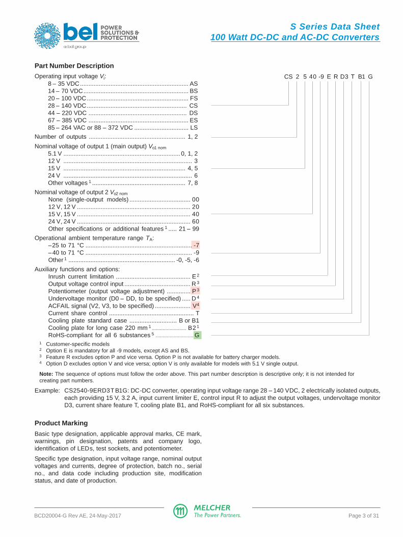
Example: CS2540-9ERD3T B1G: DC-DC converter, operating input voltage range 28 – 140 VDC, 2 electrically isolated outputs,each providing 15 V, 3.2 A, input current limiter E, control input R to adjust the output voltages, undervoltage monitorD3, current share feature T, cooling plate B1, and RoHS-compliant for all six substances.
Product Marking
Basic type designation, applicable approval marks, CE mark,warnings, pin designation, patents and company logo,identification of LEDs, test sockets, and potentiometer.
Specific type designation, input voltage range, nominal outputvoltages and currents, degree of protection, batch no., serialno., and data code including production site, modificationstatus, and date of production.
Part Number Description
Operating input voltage Vi:8 – 35 VDC ................................................................ AS14 – 70 VDC .............................................................. BS20 – 100 VDC ............................................................ FS28 – 140 VDC ........................................................... CS44 – 220 VDC .......................................................... DS67 – 385 VDC ........................................................... ES85 – 264 VAC or 88 – 372 VDC ................................ LS
Number of outputs ......................................................... 1, 2
Nominal voltage of output 1 (main output) Vo1 nom
5.1 V ..................................................................... 0, 1, 212 V ............................................................................ 315 V ........................................................................ 4, 524 V ............................................................................ 6Other voltages 1 ....................................................... 7, 8
Nominal voltage of output 2 Vo2 nom
None (single-output models) .................................... 0012 V, 12 V ................................................................... 2015 V, 15 V ................................................................... 4024 V, 24 V ................................................................... 60Other specifications or additional features 1 ..... 21 – 99
Operational ambient temperature range TA:–25 to 71 °C ............................................................... -7–40 to 71 °C ............................................................... -9Other 1 ............................................................... -0, -5, -6
Auxiliary functions and options:Inrush current limitation ............................................ E 2
Output voltage control input ....................................... R 3
Potentiometer (output voltage adjustment) .............. P 3
Undervoltage monitor (D0 – DD, to be specified) ..... D 4
ACFAIL signal (V2, V3, to be specified) ..................... V 4
Current share control .................................................. TCooling plate standard case ............................ B or B1Cooling plate for long case 220 mm 1 ............................. B2 1
RoHS-compliant for all 6 substances 5 ................................ G1 Customer-specific models2 Option E is mandatory for all -9 models, except AS and BS.3 Feature R excludes option P and vice versa. Option P is not available for battery charger models.4 Option D excludes option V and vice versa; option V is only available for models with 5.1 V single output.
Note: The sequence of options must follow the order above. This part number description is descriptive only; it is not intended forcreating part numbers.
CS 2 5 40 -9 E R D3 T B1 G

S Series Data Sheet100 Watt DC-DC and AC-DC Converters
BCD20004-G Rev AE, 24-May-2017 Page 4 of 31MELCHERThe Power Partners.
Inp
ut
filte
r
Co
ntr
ol circu
it
2
4
Opt. P
3
Fo
rwa
rd c
on
ve
rte
r (a
pp
rox.
12
0 k
Hz)
CY
16
18
20
22
12
4
6
8
10
14
Ou
tpu
tfilte
r
1
26
28
30
32
24
– +
CYVi+
Vi–
R
i
D/V
T
03057b
S+
Vo+
Vo–
S–
Fu
se
4N
4L
CY
CY
+
Brid
ge
re
ctifie
r 4
Ci
Co
ntr
ol circu
it
1
2
Opt. P
3
Fo
rwa
rd c
on
ve
rte
r(a
pp
rox.
12
0 k
Hz)
16
18
20
22
12
14
4
6
8
10
Ou
tpu
t 2
filte
r
Ou
tpu
t 1filte
r
26
28
30
32
24
– +
R
i
D
T
Vi+
Vi–
03058b
Vo1+
Vo1–
Vo2+
Vo2–
Inp
ut
filte
r
4
4N
4L
CY
CY
CY
CY CY
CY
+
Fu
se
Brid
ge
re
ctifie
r 4
Ci
Functional DescriptionThe input voltage is fed via an input fuse, an input filter, abridge rectifier (LS models only), and an inrush current limiterto the input capacitor C1. This capacitor sources a single-transistor forward converter with a special clamping circuit andprovides the power during the hold-up time.
Each output is powered by a separate secondary winding ofthe main transformer. The resultant voltages are rectified and
their ripple smoothed by a power choke and an output filter. Thecontrol logic senses the main output voltage Vo1 and generates,with respect to the maximum admissible output currents, thecontrol signal for the switching transistor of the forwardconverter.
The second output of double-output models is tracking to themain output, but has its own current limiting circuit. If the mainoutput voltage drops due to current limitation, the secondoutput voltage will fall as well and vice versa.
Fig. 1Block diagram of single-output converters
1 Transient suppressor (VDR)2 Suppressor diode (AS, BS, FS models)3 For CS, DS, ES, LS: Either NTC (-7 models only) or option E4 LS models only
Fig. 2Block diagram of double-output models
1 Transient suppressor (VDR)2 Suppressor diode (AS, BS, FS models)3 For CS, DS, ES, LS: Either NTC (-7 models only) or option E4 LS models only
S Series Data Sheet100 Watt DC-DC and AC-DC Converters
BCD20004-G Rev AE, 24-May-2017 Page 5 of 31MELCHERThe Power Partners.
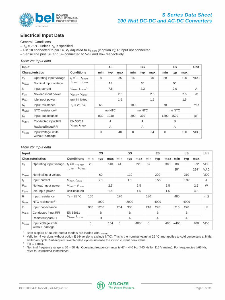
Electrical Input DataGeneral Conditions– TA = 25°C, unless TC is specified.– Pin 18 connected to pin 14, Vo adjusted to Vo nom (if option P); R input not connected.– Sense line pins S+ and S– connected to Vo+ and Vo– respectively.
Table 2a: Input data
Input AS BS FS Unit
Characteristics Conditions min typ max min typ max min typ max
V i Operating input voltage Io = 0 – Io nom 8 35 14 70 20 100 VDC
V i nom Nominal input voltage TC min –TC max 15 30 50
I i Input current Vi nom, Io nom 1 7.5 4.3 2.6 A
P i 0 No-load input power Vi min – Vi max 2.5 2.5 2.5 W
P i inh Idle input power unit inhibited 1.5 1.5 1.5
R i Input resistance TC = 25 °C 65 100 70 mΩ
RNTC NTC resistance 2 no NTC no NTC no NTC
C i Input capacitance 832 1040 300 370 1200 1500 µF
V i RFI Conducted input RFI EN 55011 A A B
Radiated input RFI V i nom, Io nom A A A
V i abs Input voltage limits 0 40 0 84 0 100 VDCwithout damage
Table 2b: Input data
Input CS DS ES LS Unit
Characteristics Conditions min typ max min typ max min typ max min typ max
V i Operating input voltage Io = 0 – Io nom 28 140 44 220 67 385 88 372 VDCTC min – TC max 854 2644 VAC
V i nom Nominal input voltage 60 110 220 310 VDC
I i Input current Vi nom, Io nom 1 2.1 1.1 0.55 0.37 A
P i 0 No-load input power Vi min – Vi max 2.5 2.5 2.5 2.5 W
P i inh Idle input power unit inhibited 1.5 1.5 1.5 4.5
R i Input resistance TC = 25 °C 150 170 180 480 mΩ
RNTC NTC resistance 2 1000 2000 4000 4000
C i Input capacitance 960 1200 264 330 216 270 216 270 µF
V i RFI Conducted input RFI EN 55011 B B B B
Radiated input RFI V i nom, Io nom B A A A
V i abs Input voltage limits 0 154 0 400 3 0 400 –400 400 VDCwithout damage
1 Both outputs of double-output models are loaded with Io nom.2 Valid for -7 versions without option E (-9 versions exclude NTC). This is the nominal value at 25 °C and applies to cold converters at initial
switch-on cycle. Subsequent switch-on/off cycles increase the inrush current peak value.3 For 1 s max.4 Nominal frequency range is 50 – 60 Hz. Operating frequency range is 47 – 440 Hz (440 Hz for 115 V mains). For frequencies ≥ 63 Hz,
refer to Installation Instructions.
S Series Data Sheet100 Watt DC-DC and AC-DC Converters
BCD20004-G Rev AE, 24-May-2017 Page 6 of 31MELCHERThe Power Partners.
Input Transient Protection
A suppressor diode or a VDR (depending upon the inputvoltage range) together with the input fuse and a symmetricalinput filter form an effective protection against high inputtransient voltages which, typically occur in most installations,but especially in battery-driven mobile applications.
Standard nominal battery voltages are: 12, 24, 36, 48, 60, 72,110, and 220 V. Railway batteries are specified with a toleranceof –30% to +25%, with short excursions up to ±40%.
In certain applications, additional surges according to RIA 12are specified. The power supply must not switch off duringthese surges, and since their energy can practically not beabsorbed, an extremely wide input range is required. The ESinput range for 110 V batteries has been designed and testedto meet this requirement.
Input Fuse
A fuse mounted inside the converter protects against severedefects. This fuse may not fully protect the converter, when theinput voltage exceeds 200 VDC. In applications, where theconverters operate at source voltages above 200 VDC, anexternal fuse or a circuit breaker at system level should beinstalled.
Table 3: Fuse Specification
Model Fuse type Reference Rating
AS fast-blow 1 Littlefuse 314 30 A, 125 VBS fast-blow 1 Littlefuse 314 25 A, 125 VFS slow-blow 2 Schurter SPT 16 A, 250 VCS slow-blow 2 Schurter SPT 12.5 A, 250 VDS slow-blow 2 Schurter SPT 8 A, 250 VES slow-blow 2 Schurter SPT 4 A, 250 VLS slow-blow 2 Schurter SPT 4 A, 250 V
1 Fuse size 6.3 × 32 mm 2 Fuse size 5 × 20 mm
Fig. 3Typical inrush current versus time at Vi max, Rext = 0 Ω.For AS, BS, FS, and for application-related values, use theformula in this section to get realistic results.
Inrush Current Limitation
The FS, CS, DS, ES, LS models incorporate an NTC resistor inthe input circuitry, which at initial turn-on reduces the peakinrush current value by a factor of 5 – 10 such protectingconnectors and switching devices from damage. Subsequentswitch-on cycles within short periods will cause an increase ofthe peak inrush current value due to the warming-up of the NTCresistor. See also Option E.
The inrush current peak value (initial switch-on cycle) can bedetermined by following calculation; see also fig. 3:
Vi sourceIinr p = ––––––––––––––––(Rs ext + Ri + RNTC)
Fig. 4Equivalent input ciruit
Rs ext Ri RNTCIinr p
Vi source
+Ci int
05109a
Static Input Current Characteristic
Reverse Polarity
The converters (except LS models) are not protected againstreverse polarity at the input to avoid unwanted power losses. Ingeneral, only the input fuse will trip.
LS models are fully protected by the built-in bridge rectifier.
Fig. 5Typical input current versus relative input voltage
2 3 4 5 61
1
2
5
10
FS
CS
ES
LS (DC input)
Vi
Vi min
Ii (A)
DS
20
0.5
AS
BS
04037a
1 2 3 t [ms]0
50
100
Ii inr [A]
150
CSES, LSDS
04038a
0.1
S Series Data Sheet100 Watt DC-DC and AC-DC Converters
BCD20004-G Rev AE, 24-May-2017 Page 7 of 31MELCHERThe Power Partners.
Fig. 6aTypical hold-up time t h versus relative DC input voltage.Vi/Vi min. DC-DC converters require an external series diodein the input path, if other loads are connected to the sameinput supply lines.
Input Under-/Overvoltage Lockout
If the input voltage remains below approx. 0.8 Vi min or exceedsapprox. 1.1 Vi max, an internally generated inhibit signaldisables the output(s). When checking this function, theabsolute maximum input voltage V i abs should be observed.Between Vi min and the undervoltage lock-out level the outputvoltage may be below the value defined in table ElectricalOutput data.
Hold-Up Time
Fig. 6bTypical hold-up time t h versus relative AC input voltage (LSmodels)
2 3 4 5 610.30
1
Vi–––––Vi min
th [ms]
10
100
DS
CSES
FS
ASBS
04041a
2 3 412
Vi _______
Vi min
th [ms]
10
10004049a

S Series Data Sheet100 Watt DC-DC and AC-DC Converters
BCD20004-G Rev AE, 24-May-2017 Page 8 of 31MELCHERThe Power Partners.
Electrical Output DataGeneral Conditions:– TA = 25 °C, unless TC is specified.– Pin 18 (i) connected to pin 14 (S– or Vo1–), R input not connected, Vo adjusted to Vo nom (option P),– Sense line pins 12 (S+) and 14 (S–) connected to pins 4 (Vo1+) and 8 (Vo1–), respectively.
Table 5: Output data of single-output models
Model AS – LS1001 AS – LS1301/17405 AS – LS1501 AS – LS1601 UnitNom. output voltage 5.1 V 12 V / 12.84 V 5 15 V 24 V
Characteristics Conditions min typ max min typ max min typ max min typ max
Vo Output voltage Vi nom, Io nom 5.07 5.13 11.935 12.075 14.91 15.09 23.86 24.14 V
Vo BR Overvoltage protection 6.0 15.2/17.55 19.6 28.5(suppressor diode)7
Io nom Output current nom. 1 Vi min – Vi max 16 8/7.55 6.5 4.2 ATC min – TC max
IoL Output current limit Vi min – Vi max 16.2 8.2/7.7 5 6.7 4.4
vo Output Low frequency8 Vi nom, Io nom 5 5 5 5 mVpp
noise 3Switching frequ. BW = 20 MHz 10 5 5 5
Total incl. spikes 50 50 60 90
∆Vo u Static line regulation Vi min – Vi max ±15 ±20 ±25 ±30 mVwith respect to Vi nom Io nom
∆Vo I Static load regulation 10 Vi nom –20 –25 –30 –40(0.1 – 1) Io nom
vo d Dynamic Voltage Vi nom ±100 ±100 ±100 ±100load deviation 6 Io nom ↔ 1/2 Io nom
t dregulat.3
Recovery time6 0.4 0.5 0.5 0.5 ms
αv o Temperature coefficient TC min – TCmax ±0.02 ±0.02 ±0.02 ±0.02 %/Kof output voltage 4 Io nom
1 If the output voltages are increased above Vo nom through R-input control, option P setting, remote sensing or option T, the output currentsshould be reduced accordingly so that Po nom is not exceeded.
2 See Output voltage regulation3 Measured according to IEC/EN 61204 with a probe according to annex A4 For battery charger applications, a defined negative temperature coefficient can be provided by using a temperature sensor (see
Accessories), but we recommend choosing the special battery charger models.5 Especially designed for battery charging using the temperature sensor (see Accessories). Vo is set to 12.84 V ±1% (R-input open)6 See Dynamic load regulation7 Breakdown voltage of the incorporated suppressor diode (1 mA; 10 mA for 5 V output). Exceeding Vo BR is dangerous for the
suppressor diode.8 LS models only (twice the input frequency)
S Series Data Sheet100 Watt DC-DC and AC-DC Converters
BCD20004-G Rev AE, 24-May-2017 Page 9 of 31MELCHERThe Power Partners.
1 Breakdown voltage of theincorporated suppressor diodes(1 mA). Exceeding Vo BR isdangerous for the suppressordiodes.
2 If the output voltages areincreased above Vo nom via R-input control, option P setting,remote sensing, or option T, theoutput currents should bereduced accordingly, so thatPo nom is not exceeded.
3 Measured according to IEC/EN61204 with a probe annex A
4 See Dynamic Load Regulation5 See Output Voltage Regulation
of Double-Output Models6 For battery charger
applications, a defined negativetemperature coefficient can beprovided by using atemperature sensor; seeAccessories.
7 Especially designed for batterycharging using the batterytemperature sensor; seeAccessories.Vo1 is set to 25.68 V ±1% (R-input open-circuit).
8 LS models only (twice theinput frequency)
9 Both outputs connected inseries.
Table 6b: Output data of double-output models. General conditions as per table 5.
Model AS – LS2660 / 2740 7 UnitNom. output voltage 2 ××××× 24 V / 2 ××××× 25.68 V 7
Output 1 Output 2
Characteristics Conditions min typ max min typ max
Vo Output voltage Vi nom, Io1 nom, Io2 nom 23.86 7 24.14 7 23.64 7 24.36 7 V
Vo BR1 Overvoltage protection 28.5/347 28.5/347
(suppressor diode)
Io nom Output current nom. 2 Vi min – Vi max 2/ 1.8 7 2 /1.8 7 ATC min – TC max
IoL Output current limit 9 Vi min – Vi max 2 .2/ 2.0 7 2 .2/2.0 7
vo Output Low frequency8 Vi nom, Io nom 5 5 mVppnoise 3
Switching freq. BW = 20 MHz 5 5
Total incl. spikes 50 50
∆Vo u Static line regulation Vi min – Vi max ±30 5 mVwith respect to Vi nom Io nom
∆Vo I Static load regulation Vi nom –60 5
(0.1 – 1) Io nom
vo d Dynamic Voltage Vi nom ±100 ±150load deviation 4 Io1 nom ↔ 1/2 Io1 nom
t dregulat. Recovery time4 1/2 Io2 nom 0.2 ms
αv o Temperature coefficient TC min – TC max ±0.02 %/Kof output voltage 6 Io nom
Table 6a: Output data of double-output models. General conditions as per table 5.
Model AS – LS2320 AS – LS2540 UnitNom. output voltage 2 ××××× 12 V 2 ××××× 15 V
Output 1 Output 2 Output 1 Output 2
Characteristics Conditions min typ max min typ max min typ max min typ max
Vo Output voltage Vi nom, Io1 nom, Io2 nom 11.93 12.07 11.82 12.18 14.91 15.09 14.78 15.22 V
Vo BR1 Overvoltage protection 15.2 15.2 19.6 19.6
(suppressor diode)
Io nom Output current nom.2 Vi min – Vi max 4 4 3.2 3.2 ATC min – TC max
IoL Output current limit 9 Vi min – Vi max 4.2 4.2 3.4 3.4
vo Output Low frequency8 Vi nom, Io nom 5 5 5 5 mVppnoise 3
Switching freq. BW = 20 MHz 5 5 5 5
Total incl. spikes 40 40 50 50
∆Vo u Static line regulation Vi min – Vi max ±20 5 ±25 5 mVwith respect to Vi nom Io nom
∆Vo I Static load regulation Vi nom –40 5 –50 5
(0.1 – 1) Io nom
vo d Dynamic Voltage Vi nom, ±100 ±150 ±100 ±150load deviation 4 Io1 nom ↔ 1/2 Io1 nom
t dregulat. Recovery time 4 1/2 Io2 nom 0.2 0.2 ms
αv o Temperature coefficient TC min – TC max ±0.02 ±0.02 %/Kof output voltage 6 Io nom

S Series Data Sheet100 Watt DC-DC and AC-DC Converters
BCD20004-G Rev AE, 24-May-2017 Page 10 of 31MELCHERThe Power Partners.
Vo/Vo nom
0.98
0.5
00.5 1.0
Io1
IoL
Io/Io nom
05098a
0
0.2
0.4
0.6
0.8
50 60 70 80 90 100
Io/Io nom
TA [°C]
1.0
Forced
cooling
05089a
TA min
TC max
Convection cooling
Fig. 7Output current derating versus temperature for -7 and -9models.
Thermal Considerations
If a converter is located in free, quasi-stationary air (convectioncooling) at the indicated maximum ambient temperature TA max
(see table Temperature specifications) and is operated at itsnominal input voltage and output power, the temperaturemeasured at the Measuring point of case temperature TC (seeMechanical Data) will approach the indicated value TC max afterthe warm-up phase. However, the relationship between TA andTC depends heavily upon the conditions of operation andintegration into a system. The thermal conditions areinfluenced by input voltage, output current, airflow, andtemperature of surrounding components and surfaces. TA max
is therefore, contrary to TC max, an indicative value only.
Caution: The installer must ensure that under all operatingconditions TC remains within the limits stated in the tableTemperature specifications.
Notes: Sufficient forced cooling or an additional heat sink allowsTA to be higher than 71 °C (e.g., 85 °C), as long as TC max is notexceeded. Details are specified in fig.7
applied overvoltages. Overload at any of the outputs will causea shut-down of all outputs. A red LED indicates the overloadcondition.
Note: Vo BR is specified in Electrical Output Data. If this voltage isexceeded, the suppressor diode generates losses and maybecome a short circuit.
Parallel and Series Connection
Single- or double-output models with equal output voltage canbe connected in parallel using option T (current sharing). If the Tpins are interconnected, all converters share the output currentequally.
Single-output models and/or main and second outputs ofdouble-output models can be connected in series with anyother (similar) output.
Notes:
– Parallel connection of double-output models should alwaysinclude both, main and second output to maintain goodregulation.
– Not more than 5 converters should be connected in parallel.
– Series connection of second outputs without involving their mainoutputs should be avoided, as regulation may be poor.
– The maximum output current is limited by the output with thelowest current limitation, if several outputs are connected inseries.
Fig. 8Output characteristic Vo versus Io (single-output models ordouble-output models with parallel-connected outputs).
Thermal Protection
A temperature sensor generates an internal inhibit signal,which disables the outputs, when the case temperatureexceeds TC max. The outputs automatically recover, when thetemperature drops below this limit.
Continuous operation under simultaneous extreme worst-caseconditions of the following three parameters should beavoided: Minimum input voltage, maximum output power, andmaximum temperature.
Output Protection
Each output is protected against overvoltages, which couldoccur due to a failure of the internal control circuit. Voltagesuppressor diodes (which under worst case condition maybecome a short circuit) provide the required protection. Thesuppressor diodes are not designed to withstand externally

S Series Data Sheet100 Watt DC-DC and AC-DC Converters
BCD20004-G Rev AE, 24-May-2017 Page 11 of 31MELCHERThe Power Partners.
Fig. 10Models with 2 outputs 12 V: Vo2 versus Io2 with various Io1 (typ)
Fig. 11Models with 2 outputs 15 V: Vo2 versus Io2 with various Io1 (typ)
Fig. 12Models with 2 outputs 24 V: Vo2 versus Io2 with various Io1 (typ)
Fig. 9Typical dynamic load regulation of Vo.
Output Voltage Regulation
figure 9 applies to single-output or double-output models withparallel-connected outputs.
For independent configuration, output 1 is under normalconditions regulated to Vo nom, irrespective of the outputcurrents.
Vo2 depends upon the load distribution. If both outputs areloaded with more than 10% of Io nom, the deviation of Vo2
remains within ±5% of Vo1. Fig. 10 to 12 show the regulationdepending on load distribution.
Two outputs of a double-output model connected in parallelbehave like the output of a single-output model.
Note: If output 2 is not used, connect it in parallel with output 1!This ensures good regulation and efficiency.
Vod
Vod
td td
Vo ±1% Vo ±1%
t
t
≥ 10 µs ≥ 10 µs
Vo
0
0.5
1
Io/Io nom
05102c
0 1 2 3 4 5
Io2 [A]11.25
11.50
11.75
12.0
12.25
12.50
12.75
Vo2 [V]
Io1 = 4.0 AIo1 = 3.1 AIo1 = 2.2 AIo1 = 1.3 AIo1 = 0.4 A
05136a
Vo2 [V]
Io2 [A]
0 1 2 3
23
23.5
24
24.5
25
25.5
26Io1 = 2.00 AIo1 = 1.55 AIo1 = 1.10 AIo1 = 0.65 AIo1 = 0.20 A
05138a
0 1 2 3 4
Io2 [A]14.25
14.5
14.75
15.0
15.25
15.5
15.75
16.0
Vo2 [V]
Io1 = 3.2 AIo1 = 2.5 AIo1 = 1.7 AIo1 = 1.0 AIo1 = 0.3 A
05137a
S Series Data Sheet100 Watt DC-DC and AC-DC Converters
BCD20004-G Rev AE, 24-May-2017 Page 12 of 31MELCHERThe Power Partners.
R
Vext
Vi+
Vi–
Rext
R'ext
14
16
14
+
S+/Vo1+
S–/Vo1–
R
12
05074a
Vi–
Vi+
–
16
S–/Vo1–
0 t
t0
Inhibit
1
0.1
1Vo/Vo nom
tr tf
06001
1.6
0.8
0
–0.8Vinh [V]
Iinh [mA]
–40 0–20 20 40
2.0
1.2
0.4
–0.4
Vinh = 0.8 V
Vo = on Vo = off
Vinh = 2.4 V
06
03
2a
Auxiliary Functions
Inhibit for Remote On/Off
The outputs may be enabled or disabled by means of a logicsignal (TTL, CMOS, etc.) applied between the inhibit input i(pin 18) and pin 14 (S– or Vo1–). In systems with severalconverters, this feature can be used to control the activationsequence of the converters. If the inhibit function is notrequired, connect the inhibit pin 18 with pin 14!
Note: If pin 18 is not connected, the output is disabled.
Fig. 13Definition of Vinh and Iinh.
Table 7: Inhibit characteristics
Characteristic Conditions min typ max Unit
Vinh Inhibit Vo = on Vi min – Vi max – 50 0.8 Vvoltage Vo = off 2.4 50
I inh Inhibit current Vinh = 0 – 400 µA
t r Rise time 30 ms
t f Fall time depending on Io
Fig. 15Output response as a function of inhibit control
Fig. 14Typical inhibit current I inh versus inhibit voltage Vinh
Table 7: Maximum voltage compensation allowed usingsense lines
Output Total voltage difference Voltage difference voltage between sense lines and between
their respective outputs Vo– and S–
5.1 V <0.5 V <0.25 V
12 V, 15 V, 24 V <1.0 V <0.25 V
Sense Lines (Single-Output Models)
Important: Sense lines must always be connected! Incorrectlyconnected sense lines may activate the overvoltage protectionresulting in a permanent short-circuit of the output.
This feature allows for compensation of voltage drops acrossthe connector contacts and if necessary, across the load lines.We recommend connecting the sense lines directly at thefemale connector.
To ensure correct operation, both sense lines (S+, S–) shouldbe connected to their respective power outputs (Vo+ and Vo–),and the voltage difference between any sense line and itsrespective power output (as measured on the connector)should not exceed the following values:
Programmable Output Voltage (R-Function)
As a standard feature, the converters offer an adjustableoutput voltage, identified by letter R in the type designation.The control input R (pin 16) accepts either a control voltageVext or a resistor Rext to adjust the desired output voltage.When input R is not connected, the output voltage is set to Vo
nom.
a) Adjustment by means of an external control voltage Vext
between pin 16 (R) and pin 14 (S–):
The control voltage range is 0 – 2.75 VDC and allows for anadjustment in the range of approximately 0 – 110% of Vo nom.
VoVext ≈ –––––– • 2.5 VVo nom
Fig. 16Output voltage control for single-output models
S–/Vo1–
i
Vo+
Iinh
Vinh
06031b
14
18
Inp
ut

S Series Data Sheet100 Watt DC-DC and AC-DC Converters
BCD20004-G Rev AE, 24-May-2017 Page 13 of 31MELCHERThe Power Partners.
Table 8a: Rext for Vo < Vo nom; approximate values (Vi nom, Io nom, series E 96 resistors); R'ext = not fitted
Vo nom = 5.1 V Vo nom = 12 V Vo nom = 15 V Vo nom = 24 V
Vo [V] Rext [kΩΩΩΩΩ] Vo [V] 1 Rext [kΩΩΩΩΩ] Vo [V] 1 Rext [kΩΩΩΩΩ] Vo [V] 1 Rext [kΩΩΩΩΩ]
0.5 0.432 2 4 0.806 2 4 0.619 4 8 0.8061.0 0.976 3 6 1.33 4 8 1.47 6 12 1.331.5 1.65 4 8 2 6 12 2.67 8 16 2.02.0 2.61 5 10 2.87 8 16 4.53 10 20 2.872.5 3.83 6 12 4.02 9 18 6.04 12 24 4.023.0 5.76 7 14 5.62 10 20 8.06 14 28 5.623.5 8.66 8 16 8.06 11 22 11 16 32 8.064.0 14.7 9 18 12.1 12 24 16.2 18 36 12.14.5 30.1 10 20 20 13 26 26.1 20 40 205.0 200 11 22 42.2 14 28 56.2 22 44 44.2
Table 8b: R’ext for Vo > Vo nom; approximate values (Vi nom, Io nom, series E 96 resistors); Rext = not fitted
Vo nom = 5.1 V Vo nom = 12 V Vo nom = 15 V Vo nom = 24 V
Vo [V] R'ext [kΩΩΩΩΩ] Vo [V] 1 R'ext [kΩΩΩΩΩ] Vo [V] 1 R'ext [kΩΩΩΩΩ] Vo [V] 1 R'ext [kΩΩΩΩΩ]
5.15 432 12.1 24.2 1820 15.2 30.4 1500 24.25 48.5 33205.2 215 12.2 24.4 931 15.4 30.8 768 24.5 49.0 16905.25 147 12.3 24.6 619 15.6 31.2 523 24.75 49.5 11305.3 110 12.4 24.8 475 15.8 31.6 392 25.0 50.0 8455.35 88.7 12.5 25.0 383 16.0 32.0 316 25.25 50.5 6985.4 75 12.6 25.2 316 16.2 32.4 267 25.5 51.0 5905.45 64.9 12.7 25.4 274 16.4 32.8 232 25.75 51.5 5115.5 57.6 12.8 25.6 243 16.5 33.0 221 26.0 52.0 442
13.0 26.0 196 26.25 52.5 40213.2 26.4 169 26.4 52.8 383
1 First column: Vo or Vo1; second column: double-output models with series-connected outputs
R'extRext
14
16
Vo1–
Vo1+
R
Vo2–
Vo2–
Vo2+
Vo2+
12
10
8
6
4 +
–
Vo1
24 V30 V48 V
Co
06004a
Fig. 17Double-output models:Wiring of the R-input for output voltages 24 V, 30 V, or 48 Vwith both outputs in series. A ceramic capacitor (Co) acrossthe load reduces ripple and spikes.
b) Adjustment by means of an external resistor:
Depending upon the value of the required output voltage,the resistor shall be connected
either: Between pin 16 and pin 14 to achieve an outputvoltage adjustment range of approximately 0 – 100% of Vo nom.
or: Between pin 16 and pin 12 to achieve an output voltageadjustment range of 100 – 110% of Vo nom.
Warnings:
– Vext shall never exceed 2.75 VDC.
– The value of R'ext shall never be less than the lowest value asindicated in table R'ext (for V0 > V0 nom) to avoid damage to theconverter!
Notes:
– The R-Function excludes option P (output voltage adjustment bypotentiometer).
If the output voltages are increased above Vo nom via R-inputcontrol, option P setting, remote sensing, or option T, the outputcurrents should be reduced, so that Po nom is not exceeded.
– With double-output models, the second output follows thevoltage of the controlled main output.
– In case of parallel connection the output voltages should beindividually set within a tolerance of 1 – 2%.
Test Sockets
Test sockets (pin diameter 2 mm) for measuring the mainoutput voltage Vo or Vo1 are located at the front of the converter.
The positive test socket is protected by a series resistor (see:Functional Description, block diagrams).
The voltage measured at the test jacks is slightly lower thanthe value at the output terminals.
S Series Data Sheet100 Watt DC-DC and AC-DC Converters
BCD20004-G Rev AE, 24-May-2017 Page 14 of 31MELCHERThe Power Partners.
2.10
2.15
2.20
2.25
2.30
2.35
2.40
2.45Cell voltage [V]
–20 –10 0 10 20 30 40 50 °C
06139b
VC = 2.27 V, –3 mV/K VC = 2.27 V, –3.5 mV/KVC = 2.23 V, –3 mV/K VC = 2.23 V, –3.5 mV/K
Vo safe
Display Status of LEDs
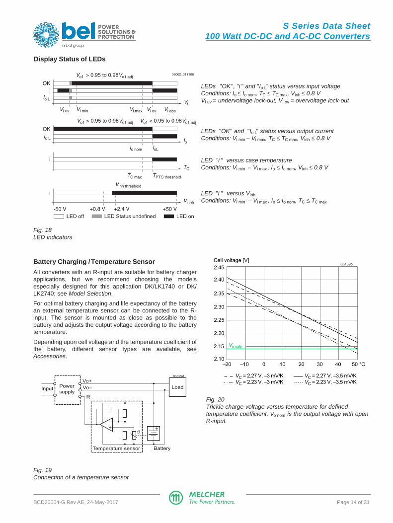
Battery Charging /Temperature Sensor
All converters with an R-input are suitable for battery chargerapplications, but we recommend choosing the modelsespecially designed for this application DK/LK1740 or DK/LK2740; see Model Selection.
For optimal battery charging and life expectancy of the batteryan external temperature sensor can be connected to the R-input. The sensor is mounted as close as possible to thebattery and adjusts the output voltage according to the batterytemperature.
Depending upon cell voltage and the temperature coefficient ofthe battery, different sensor types are available, seeAccessories.
Fig. 20Trickle charge voltage versus temperature for definedtemperature coefficient. Vo nom is the output voltage with openR-input.
Fig. 19Connection of a temperature sensor
Fig. 18LED indicators
LEDs "OK ", "i " and "Io L" status versus input voltageConditions: Io ≤ Io nom, TC ≤ TC max, Vinh ≤ 0.8 VVi uv = undervoltage lock-out, Vi ov = overvoltage lock-out
LEDs "OK" and "Io L" status versus output currentConditions: Vi min – Vi max, TC ≤ TC max, Vinh ≤ 0.8 V
LED "i " versus case temperatureConditions: Vi min – Vi max , Io ≤ Io nom, Vinh ≤ 0.8 V
LED "i " versus Vinh
Conditions: Vi min – Vi max , Io ≤ Io nom, TC ≤ TC max
Vo1 > 0.95 to 0.98Vo1 adj
Vi max Vi ovVi minVi uv
Vi
Vi abs
OKi
Vo1 > 0.95 to 0.98Vo1 adj
Io nom IoL
Io
OKIo L
Vo1 < 0.95 to 0.98Vo1 adj
TC
i
TC max TPTC threshold
Vi inh
i
+50 V+0.8 V +2.4 V-50 V
Vinh threshold
Io L
LED off LED onLED Status undefined
06002_011106
Powersupply
Load
–+
Input Vo–
R
Temperature sensor
ϑ
03099d
Battery
Vo+
+
S Series Data Sheet100 Watt DC-DC and AC-DC Converters
BCD20004-G Rev AE, 24-May-2017 Page 15 of 31MELCHERThe Power Partners.
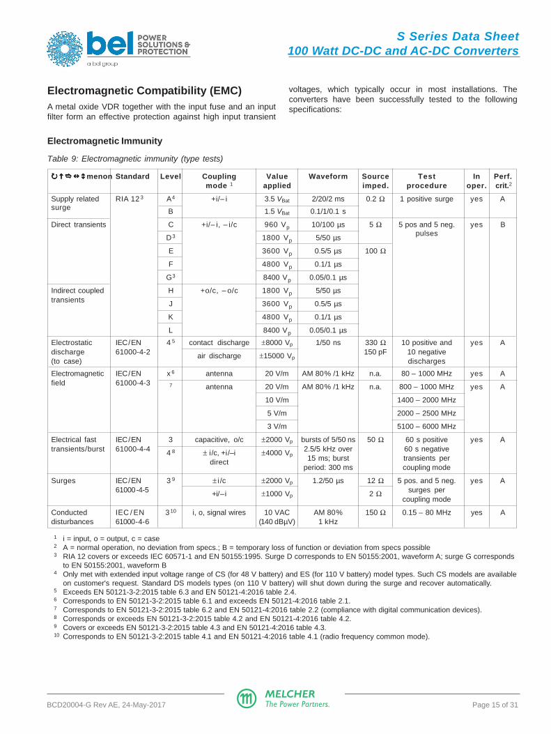
Table 9: Electromagnetic immunity (type tests)
menon Standard Level Coupling Value Waveform Source Test In Perf.mode 1 applied imped. procedure oper. crit.2
Supply related RIA 12 3 A4 +i/– i 3.5 VBat 2/20/2 ms 0.2 Ω 1 positive surge yes Asurge B 1.5 VBat 0.1/1/0.1 s
Direct transients C +i/– i, – i/c 960 Vp 10/100 µs 5 Ω 5 pos and 5 neg. yes B
D3 1800 Vp 5/50 µspulses
E 3600 Vp 0.5/5 µs 100 Ω
F 4800 Vp 0.1/1 µs
G3 8400 Vp 0.05/0.1 µs
Indirect coupled H +o/c, – o/c 1800 Vp 5/50 µstransients J 3600 Vp 0.5/5 µs
K 4800 Vp 0.1/1 µs
L 8400 Vp 0.05/0.1 µs
Electrostatic IEC/EN 4 5 contact discharge ±8000 Vp 1/50 ns 330 Ω 10 positive and yes Adischarge 61000-4-2 air discharge ±15000 Vp
150 pF 10 negative(to case) discharges
Electromagnetic IEC/EN x 6 antenna 20 V/m AM 80% /1 kHz n.a. 80 – 1000 MHz yes Afield 61000-4-3 7 antenna 20 V/m AM 80% /1 kHz n.a. 800 – 1000 MHz yes A
10 V/m 1400 – 2000 MHz
5 V/m 2000 – 2500 MHz
3 V/m 5100 – 6000 MHz
Electrical fast IEC/EN 3 capacitive, o/c ±2000 Vp bursts of 5/50 ns 50 Ω 60 s positive yes Atransients/burst 61000-4-4 4 8 ± i/c, +i/–i ±4000 Vp
2.5/5 kHz over 60 s negative
direct 15 ms; burst transients perperiod: 300 ms coupling mode
Surges IEC/EN 3 9 ± i /c ±2000 Vp 1.2/50 µs 12 Ω 5 pos. and 5 neg. yes A61000-4-5 +i/–i ±1000 Vp 2 Ω surges per
coupling mode
Conducted IEC / EN 3 10 i, o, signal wires 10 VAC AM 80% 150 Ω 0.15 – 80 MHz yes Adisturbances 61000-4-6 (140 dBµV) 1 kHz
1 i = input, o = output, c = case2 A = normal operation, no deviation from specs.; B = temporary loss of function or deviation from specs possible3 RIA 12 covers or exceeds IEC 60571-1 and EN 50155:1995. Surge D corresponds to EN 50155:2001, waveform A; surge G corresponds
to EN 50155:2001, waveform B4 Only met with extended input voltage range of CS (for 48 V battery) and ES (for 110 V battery) model types. Such CS models are available
on customer's request. Standard DS models types (on 110 V battery) will shut down during the surge and recover automatically.5 Exceeds EN 50121-3-2:2015 table 6.3 and EN 50121-4:2016 table 2.4.6 Corresponds to EN 50121-3-2:2015 table 6.1 and exceeds EN 50121-4:2016 table 2.1.7 Corresponds to EN 50121-3-2:2015 table 6.2 and EN 50121-4:2016 table 2.2 (compliance with digital communication devices).8 Corresponds or exceeds EN 50121-3-2:2015 table 4.2 and EN 50121-4:2016 table 4.2.9 Covers or exceeds EN 50121-3-2:2015 table 4.3 and EN 50121-4:2016 table 4.3.10 Corresponds to EN 50121-3-2:2015 table 4.1 and EN 50121-4:2016 table 4.1 (radio frequency common mode).
Electromagnetic Compatibility (EMC)A metal oxide VDR together with the input fuse and an inputfilter form an effective protection against high input transient
Electromagnetic Immunity
voltages, which typically occur in most installations. Theconverters have been successfully tested to the followingspecifications:

S Series Data Sheet100 Watt DC-DC and AC-DC Converters
BCD20004-G Rev AE, 24-May-2017 Page 16 of 31MELCHERThe Power Partners.
dBµV/m
10
20
30
40
0
50
TÜV-Divina, Testdistance 10 m, 2006-10-01CS1601-7R Ui=110 V, Uo=12 V Io= 8 A
JM061
30 50 100 200 500 1000 MHz
EN 55022 B
CS1601-7R, Peak Vi+, Conducted 0,15 ÷ 30 MHz, Divina, 2006-10-01
0
10
20
30
40
50
60
70
80
0.2 0.5 1 2 5 10 20 MHz
EN 55022 B
dBµV
0
10
20
30
40
50
60
70
80
dBµV LS1301-7R, Peak Vi+, Conducted 0,15 ÷ 30 MHz, Divina, 2006-11-01
EN 55022 B
0.2 0.5 1 2 5 10 20 MHz 30 50 100 200 500 1000 MHz
dBµV/m
EN 55011 A
TÜV-Divina, QP, 2006-11-01Testdistance 10 m, LS1301-7R, Uo=12 V Io= 8 A
JM057
10
20
30
40
0
50
Fig. 21aTypical conducted emissions (peak) at the positive inputaccording to EN 55011/32, measured at Vi nom and Io nom
(CS1601-7R)
Fig. 21bTypical conducted emissions (peak) at the positive inputaccording to EN 55011/32, measured at Vi nom and Io nom
(LS1301-7R).
Fig. 22bRadiated emissions according to EN 55011/32, antenna10 m distance, measured at Vi nom and Io nom (LS1301-7R)
Fig. 22aRadiated emissions according to EN 55011/32, antenna10 m distance, measured at Vi nom and Io nom (CS1601-7R)
Electromagnetic Emissions

S Series Data Sheet100 Watt DC-DC and AC-DC Converters
BCD20004-G Rev AE, 24-May-2017 Page 17 of 31MELCHERThe Power Partners.
Immunity to Environmental Conditions
Table 10: Mechanical and climatic stress
Test Method Standard Test Conditions Status
Cab Damp heat IEC/EN 60068-2-78 Temperature: 40 ±2 °C Converter notsteady state MIL-STD-810D sect. 507.2 Relative humidity: 93 +2/-3 % operating
Duration: 56 days
Kb Salt mist, cyclic IEC/EN 60068-2-52 Concentration: 5% (30 °C) for 2 h Converter not(sodium chloride Storage: 40 °C, 93% rel. humidity operatingNaCl solution) Duration: 3 cycles of 22 h
Fc Vibration IEC/EN 60068-2-6 Acceleration amplitude: 0.35 mm (10 – 60 Hz) Converter(sinusoidal) MIL-STD-810D sect. 514.3 5 gn = 49 m/s2 (60 – 2000 Hz) operating
Frequency (1 Oct/min): 10 – 2000 HzTest duration: 7.5 h (2.5 h each axis)
Fh Random vibration IEC/EN 60068-2-64 Acceleration spectral density: 0.05 gn2/Hz Converter
broad band Frequency band: 8 – 500 Hz operating(digital control) Acceleration magnitude: 4.9 gn rms
Test duration: 1.5 h (0.5 h each axis)
Ea Shock IEC/EN 60068-2-27 Acceleration amplitude: 50 gn = 490 m/s2 Converter(half-sinusoidal) MIL-STD-810D sect. 516.3 Bump duration: 11 ms operating
Number of bumps: 18 (3 each direction)
-- Shock EN 50155:2007 sect. 12.2.11, Acceleration amplitude: 5.1 gn ConverterEN 61373 sect. 10, Bump duration: 30 ms operatingclass B, body mounted 1 Number of bumps: 18 (3 in each direction)
-- Simulated long life EN 50155:2007 sect. 12.2.11, Acceleration spectral density: 0.02 gn2/Hz Converter
testing at EN 61373 sect. 8 and 9, Frequency band: 5 – 150 Hz operatingincreased random class B, body mounted 1 Acceleration magnitude: 0.8 gn rms
vibration levels Test duration: 15 h (5 h in each axis)
1 Body mounted = chassis of a railway coach
Table 11: Temperature specifications, values given are for an air pressure of 800 – 1200 hPa (800 – 1200 mbar)
Temperature -5 2 -6 2 -7 (option) -9 Unit
Characteristics Conditions min max min max min max min max
TA Ambient temperature Converter –25 50 –25 60 –25 71 –40 71 °C
TC Case temperature 1 operating –25 85 1 –25 90 1 –25 95 1 –40 95 1
TS Storage temperature Not operating –40 85 –40 85 –40 85 –55 85
1 Overtemperature lockout at TC > 95 °C2 Customer-specific models
Temperatures
Table 12: MTBF calculated according to MIL-HDBK 217F
Values at specified Model Ground benign Ground fixed Ground mobile Unitcase temperature 40 °C 40 °C 70 °C 50 °C
MTBF 1 AS – LS 500 000 150 000 80 000 50 000 h
Device hours2 AS – LS 500 000
1 Calculated according to MIL-HDBK-217F2 Statistic values, based on an average of 4300 working hours per year, over 3 years in general field use.
Reliability and Device Hours
S Series Data Sheet100 Watt DC-DC and AC-DC Converters
BCD20004-G Rev AE, 24-May-2017 Page 18 of 31MELCHERThe Power Partners.
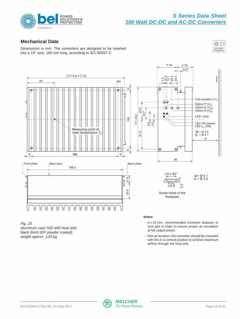
Mechanical DataDimensions in mm. The converters are designed to be insertedinto a 19" rack, 160 mm long, according to IEC 60297-3.
Notes:
– d ≥ 15 mm, recommended minimum distance tonext part in order to ensure proper air circulationat full output power.
– free air location: the converter should be mountedwith fins in a vertical position to achieve maximumairflow through the heat sink.
Fig. 23Aluminum case S02 with heat sink;black finish (EP powder coated);weight approx. 1.25 kg
EuropeanProjection
111 (
3U
)
168.5
60
4.5
19
.7
9.5
29
.95
1.5
30
.3
20
.3
12
.11
0.3
7.0
3.27
7 TE 5 TE
Test sockets (+/–)
Option P (Vo)
Option D (Vti)
LED OK (green)
LED i (red)
LED IoL (red)
Option D (Vto)
25.9
Front plate Main face Back plate
(171.0 to 171.9)
50
11.8
= Ø 3.5= Ø 4.1
152
100
M4
55
81528
09004f
Measuring point ofcase temperature TC
d
= Ø 4.1= Ø 3.5
Screw holes of thefrontplate
∅5 x 90°
∅2.8 0.2

S Series Data Sheet100 Watt DC-DC and AC-DC Converters
BCD20004-G Rev AE, 24-May-2017 Page 19 of 31MELCHERThe Power Partners.
6.5
11.2
13
140
17.3 133.4 ±0.230
168
5 47.2
38.5
127
6.5
11.8
11027
EuropeanProjection
111 (
3U
)
17.3 133.4
168
101
547.2
1585
M 4
5
Measuring point ofcase temperature TC
50
(171.0 ... 171.9)
3.27
7 TE 4 TE
09003b
38.5
11.8
Fig. 24Option B1: Aluminum case S02 with small cooling plate; black finish (EP powder coated).Suitable for mounting with access from the backside.Total weight approx. 1.2 kg.
Fig. 25Option B: Aluminum case S02 with large cooling plate; black finish (EP powder coated).Suitable for front mounting.Total weight approx. 1.3 kg
Note: Long case with option B2, elongated by 60 mm for 220 mmrack depth, is available on request. (No LEDs, no test jacks.)
S Series Data Sheet100 Watt DC-DC and AC-DC Converters
BCD20004-G Rev AE, 24-May-2017 Page 20 of 31MELCHERThe Power Partners.
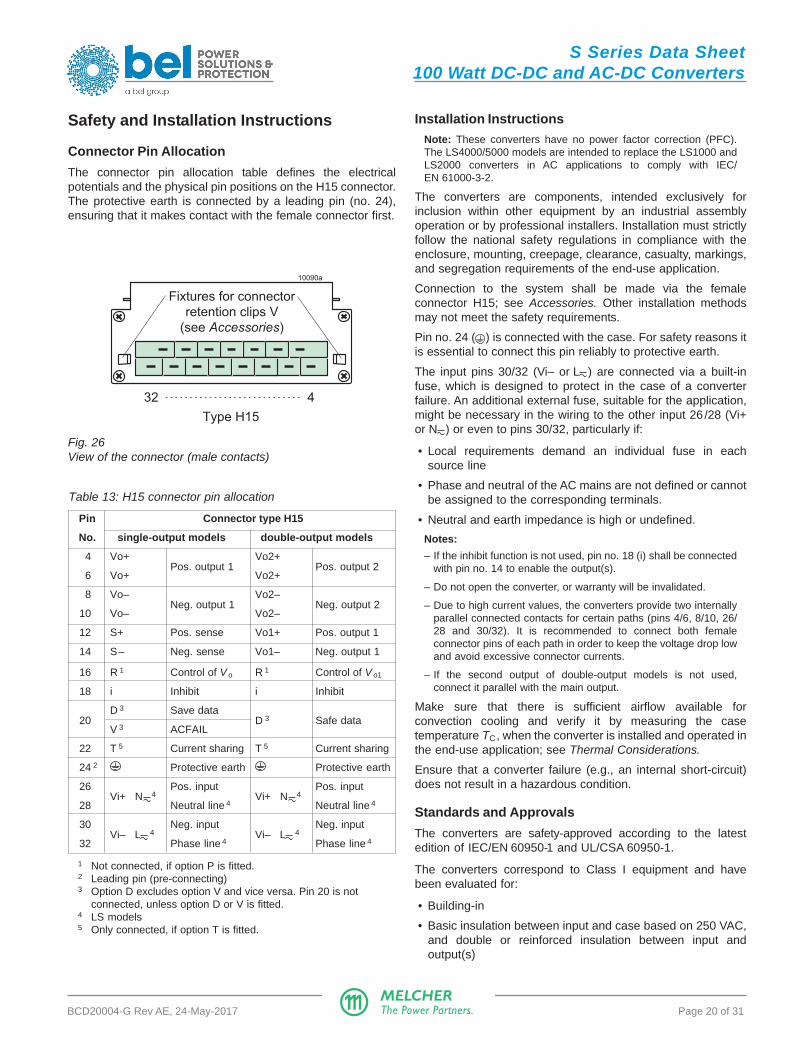
Fig. 26View of the connector (male contacts)
Safety and Installation Instructions
Connector Pin Allocation
The connector pin allocation table defines the electricalpotentials and the physical pin positions on the H15 connector.The protective earth is connected by a leading pin (no. 24),ensuring that it makes contact with the female connector first.
Installation InstructionsNote: These converters have no power factor correction (PFC).The LS4000/5000 models are intended to replace the LS1000 andLS2000 converters in AC applications to comply with IEC/EN 61000-3-2.
The converters are components, intended exclusively forinclusion within other equipment by an industrial assemblyoperation or by professional installers. Installation must strictlyfollow the national safety regulations in compliance with theenclosure, mounting, creepage, clearance, casualty, markings,and segregation requirements of the end-use application.
Connection to the system shall be made via the femaleconnector H15; see Accessories. Other installation methodsmay not meet the safety requirements.
Pin no. 24 ( ) is connected with the case. For safety reasons itis essential to connect this pin reliably to protective earth.
The input pins 30/32 (Vi– or L ) are connected via a built-infuse, which is designed to protect in the case of a converterfailure. An additional external fuse, suitable for the application,might be necessary in the wiring to the other input 26 /28 (Vi+or N ) or even to pins 30/32, particularly if:
• Local requirements demand an individual fuse in eachsource line
• Phase and neutral of the AC mains are not defined or cannotbe assigned to the corresponding terminals.
• Neutral and earth impedance is high or undefined.
Notes:
– If the inhibit function is not used, pin no. 18 (i) shall be connectedwith pin no. 14 to enable the output(s).
– Do not open the converter, or warranty will be invalidated.
– Due to high current values, the converters provide two internallyparallel connected contacts for certain paths (pins 4/6, 8/10, 26/28 and 30/32). It is recommended to connect both femaleconnector pins of each path in order to keep the voltage drop lowand avoid excessive connector currents.
– If the second output of double-output models is not used,connect it parallel with the main output.
Make sure that there is sufficient airflow available forconvection cooling and verify it by measuring the casetemperature TC, when the converter is installed and operated inthe end-use application; see Thermal Considerations.
Ensure that a converter failure (e.g., an internal short-circuit)does not result in a hazardous condition.
Standards and Approvals
The converters are safety-approved according to the latestedition of IEC/EN 60950-1 and UL/CSA 60950-1.
The converters correspond to Class I equipment and havebeen evaluated for:
• Building-in
• Basic insulation between input and case based on 250 VAC,and double or reinforced insulation between input andoutput(s)
432
Type H15
Fixtures for connectorretention clips V
(see Accessories)
10090a
Table 13: H15 connector pin allocation
Pin Connector type H15
No. single-output models double-output models
4 Vo+Pos. output 1
Vo2+Pos. output 2
6 Vo+ Vo2+
8 Vo–Neg. output 1
Vo2–Neg. output 2
10 Vo– Vo2–
12 S+ Pos. sense Vo1+ Pos. output 1
14 S– Neg. sense Vo1– Neg. output 1
16 R 1 Control of V o R 1 Control of V o1
18 i Inhibit i Inhibit
20D 3 Save data
D 3 Safe dataV 3 ACFAIL
22 T 5 Current sharing T 5 Current sharing
24 2 Protective earth Protective earth
26Vi+ N 4
Pos. input Vi+ N 4
Pos. input
28 Neutral line 4 Neutral line 4
30Vi– L 4
Neg. inputVi– L 4
Neg. input
32 Phase line 4 Phase line 4
1 Not connected, if option P is fitted.2 Leading pin (pre-connecting)3 Option D excludes option V and vice versa. Pin 20 is not
connected, unless option D or V is fitted.4 LS models5 Only connected, if option T is fitted.

S Series Data Sheet100 Watt DC-DC and AC-DC Converters
BCD20004-G Rev AE, 24-May-2017 Page 21 of 31MELCHERThe Power Partners.
• Functional insulation between outputs
• Overvoltage category II
• Pollution degree 2 environment
• Max. altitude: 2000 m
• The converters fulfill the requirements of a fire enclosure.
The converters are subject to manufacturing surveillancein accordance with the above mentioned standards and ISO9001:2008. A CB-scheme is available.
Railway Applications and Fire Protection
The converters have been designed by observing the railwaystandards EN 50155, EN 50121-3-2, and EN 50121-4. Allboards are coated with a protective lacquer.
The converters with version V108 (or later) comply with NF-F16(I2/F1). They also comply with EN 45545-1, EN 45545-2 (2013),if installed in a technical compartment or cabinet.
Protection Degree and Cleaning Liquids
Condition: Female connector fitted to the converter.
• IP 30: All models except those with option P, and exceptthose with option D or V including a potentiometer.
• IP 20: All models fitted with option P, or with option D or Vwith potentiometer.
In order to avoid damage, any penetration of cleaning fluidshas to be prevented, since the power supplies are nothermetically sealed.
Isolation and Protective Earth
The electric strength test is performed in the factory as routinetest according to EN 50514 and IEC/EN 60950 and should notbe repeated in the field. The company will not honor warrantyclaims resulting from incorrectly executed electric strengthtests. The resistance of the earth connection to the case(<0.1 Ω) is tested as well.
Leakage Currents
Leakage currents flow due to internal leakage capacitances andY-capacitors. The current values are proportional to the supplyvoltage and are specified in the table below.
Table 14: Isolation
Characteristic Input to case Output(s) to Output 1 to Unitand output(s) case output 2
Electric Factory test >1 s 2.8 1 1.4 0.15 kVDCstrength AC test voltage equivalent
2.0 1 1.0 0.1 kVAC
test to factory test
Insulation resistance at 500 VDC >300 >300 >100 2 MΩCreepage distances ≥ 3.2 3 -- -- mm
1 According to IEC/EN 60950, subassemblies connecting input to output are pre-tested with 5.6 kVDC or 4 kVAC.2 Tested at 150 VDC3 Input to outputs: 6.4 mm
LS Models Operated at Greater than 63 Hz
Above 63 Hz, the earth leakage current may exceed 3.5 mA, themaximum value allowed in IEC 60950. Frequencies ≥ 350 Hzare only permitted with Vi ≤200 VAC.
The built-in Y-caps are approved for ≤100 Hz. Safety approvalsand CB scheme cover only 50 – 60 Hz.
Table 15: Earth leakage currents for LS models
Characteristic Class I Unit
Max. leakage Permissible accord. to IEC/EN 60950 3.5 mAcurrent Typ. value at 264 V, 50 Hz 1.43

S Series Data Sheet100 Watt DC-DC and AC-DC Converters
BCD20004-G Rev AE, 24-May-2017 Page 22 of 31MELCHERThe Power Partners.
AC-DCfrontend
DC-DCcon-
verter
Mains Battery SELV
Earth connection
+
–
10044a≤150 VAC or VDC for AK, BK
≤250 VAC or VDC for CK, DK, EK, FK, LK
Fuse
Fuse
≤150 VAC or VDC for AK, BK
≤250 VAC or VDC for CK, DK, EK, FK, LK
+
Safety of Operator-Accessible Output Circuits
If the output circuit of a DC-DC converter is operator-accessible, it shall be an SELV circuit according to thestandard IEC 60950-1.
The following table shows some possible installationconfigurations, compliance with which causes the output
circuit of the converter to be an SELV circuit according to IEC60950-1 up to a configured output voltage (sum of nominalvoltages if in series or +/– configuration) of 36 V.
However, it is the sole responsibility of the installer to assure thecompliance with the applicable safety regulations.
Table 16: Safety concept leading to an SELV output circuit
Conditions Front end DC-DC converter Result
Nominal Minimum required grade Nominal DC Minimum required Types Measures to achieve the Safety statussupply of insulation, to be pro- output voltage safety status of the specified safety status of of the DC-DCvoltage vided by the AC-DC front from the front end front end output the output circuit converter
end, including mains circuit output circuitsupplied battery charger
Mains Functional (i.e. there is ≤100 V (The Primary circuit AS Double or reinforced SELV circuit≤150 V AC no need for electrical nominal voltage BS insulation, based on
insulation between the between any input the mains voltage and 2
mains supply voltage pin and earth can (provided by the DC-DCand the DC-DC converter be up to 150 V AC converter) and earthedinput voltage) or DC) case 3
Mains ≤400 V (The CS≤250 V AC nominal voltage DS
between any input ESpin and earth can FSbe up to 250 V ACor 400 V DC)
Basic ≤400 V Unearthed AS Supplementary insulation,hazardous voltage BS based on 250 V AC andsecondary circuit CS double or reinforced
DS insulation 2 (provided byES DC-DC converter) andFS earthed case 3.
Earthed Double or reinforcedhazardous voltage insulation 2 (provided bysecondary circuit the DC-DC converter)
earthed case 3
Double or reinforced ≤60 V SELV circuit Functional insulation(provided by the DC-DCconverter) 4
≤120 V TNV-3 circuit Basic insulation (providedby the DC-DC converter) 4
1 The front end output voltage should match the specified input voltage range of the DC-DC converter.2 Based on the maximum nominal output voltage from the front end.3 The earth connection has to be provided by the installer according to the relevant safety standard, e.g. IEC/EN 60950-1.4 Earthing of the case is recommended, but not mandatory.
Fig. 27Schematic safety concept.Use earth connections as per the table below.

S Series Data Sheet100 Watt DC-DC and AC-DC Converters
BCD20004-G Rev AE, 24-May-2017 Page 23 of 31MELCHERThe Power Partners.
Table 17: Safety concept leading to an SELV output circuit
Conditions AC-DC converter Installation Result
Nominal voltage Grade of insulation Measures to achieve the resulting Safety status of the AC-DCbetween input and output safety status of the output circuit converter output circuitprovided by the AC-DC converter
Mains Double or reinforced Earthed case1 and installation SELV circuit≤ 250 VAC according to the applicable standards
1 The earth connection has to be provided by the installer according to the relevant safety standards, e.g. IEC/EN 60950.
If the output circuit of an AC-DC converter is operator-accessible, it shall be an SELV circuit accord. to IEC 60950-1.
The following table shows some possible installationconfigurations, compliance with which causes the outputcircuit of LS models to be SELV according to IEC 60950-1 upto a configured output voltage (sum of nominal voltages if inseries or +/– configuration) of 36 V.
If the LS converter is used as DC-DC converter, refer to theprevious section.
AC-DCcon-
verter
Mains SELV
Earth connection
+
–
~
~
10021a
Fuse
Fuse
Fig. 28Schematic safety concept. Use earth connection as per table17. Use fuses if required by the application; see alsoInstallation Instructions.
Description of Options
Table 18: Survey of options
Option Function of option Characteristic
-7 Extended operational ambient temperature range TA = – 25 to 71 °C
E Electronic inrush current limitation circuitry Active inrush current limitation
P 2 Potentiometer for fine adjustment of output voltage Adjustment range +10/– 60% of Vo nom, excludes R input
D1 Input and/or output undervoltage monitoring circuitry Safe data signal output (D0 – DD)
V1 Input and/or output undervoltage monitoring circuitry ACFAIL signal according to VME specifications (V0, V2, V3)
T Current sharing Interconnect T-pins for parallel connection (max 5 converters)
B, B1, B2 Cooling plate (160 or 220 mm long) Replaces the standard heat sink, allowing direct chassis-mounting
non-G RoHS-compliant for 5 substances Tin-lead solder
1 Option D excludes option V and vice versa; option V only for 5.1 V outputs.2 Option P is not available for battery charger models.
-7 Temperature Range
Option -7 designates converters with an operational ambienttemperature range of –25 to 71 °C. Not for new designs.
E Inrush Current Limitation
CS/DS/ES/FS/LS models may be supplemented by anelectronic circuit (option E) replacing the standard built-in NTC

S Series Data Sheet100 Watt DC-DC and AC-DC Converters
BCD20004-G Rev AE, 24-May-2017 Page 24 of 31MELCHERThe Power Partners.
15
Ii [A]
10
5
0
–5
–10
–15
0 20 40 60 80
t [ms]
tinr
Capacitor Cifully charged
Normal operation
(FET fully conducting)
20
10065a
resistor) in order to achieve an enhanced inrush currentlimiting function. Option E is not available with AS/BS models,but mandatory for all CS/DS/ES/FS/LS models with option -9.
Fig. 29Block diagram of option ECurrent limiting resistance Rv = RS + Ri = 15 Ω
The figure below shows two consecutive peaks of the inrushcurrent, the first one is caused by Vi /Rv and the second one bythe rising current across the FET. The shape of the curvedepends on model, but the tables below show the higher ofboth peaks.
CS models fitted with option E and option D6 (input voltage
Inp
ut
Filte
r
Control
Co
nve
rte
r
FET
Ci
RiRS
JM060
LS models
+
monitor) meet the standard ETS 300132-2 for 48 VDCsupplies. Option D6 is necessary to disable the converter at lowinput voltage, such avoiding an excessive input current.Connect output D (pin 20) with inhibit (pin 18).
Option D6 should be adjusted with the potentiometer to athreshold of 36 – 40.5 V for 48 V batteries and to 44 – 50 V for60 V batteries. Refer also to the description of option D.
Note: Subsequent switch-on cycles at start-up are limited to max.10 cycles during the first 20 seconds (cold converter) and then tomax. 1 cycle every 8 s.
LS models powered by 230 VAC /50 Hz exhibit an inrushcurrent as per the fig. below, when switched on at the peak ofVi. In this case, the inrush current I inr p is 21.7 A and its durationtinr is 5 ms. This is the worst case.
If the LS converter is switched on in a different moment, Iinr p ismuch lower, but tinr rises up to 10 ms.
P Potentiometer
A potentiometer provides an output voltage adjustment rangeof +10/–60% of Vo nom. It is accessible through a hole in thefront cover. Option P is not available for battery charger modelsand is not recommended for converters connected in parallel.
Option P excludes the R-function. With double-output models,both outputs are influenced by the potentiometer (doubling thevoltage, if the outputs are connected in series).
Note: If the output voltages are increased above Vo nom via R inputcontrol, option P setting, remote sensing, or option T, the output
Fig. 31Inrush current for LS models with option E (AC supply)Vi = 230 VAC, f i = 50 Hz, Po = Po nom
Table 19a: Inrush current at Vi nom (DC supply) and Io nom
Characteristics FS CS DS E S LS Unit
Vi nom Input voltage 50 60 110 220 310 V
I inr p Peak inrush current 7.5 6.5 7.4 14.6 21 A
t inr Inrush current duration 20 25 14 16 16 ms
Table 19b: Inrush current at Vi max (DC supply) and Io nom
Characteristics FS CS DS E S LS Unit
Vi nom Input voltage 100 140 220 385 372 V
I inr p Peak inrush current 10 9 14.5 25.7 24.8 A
t inr Inrush current duration 26 30 14 12 16 ms
Iinr [A]
Vi /Rv
tinr
t [ms]
Normal operation
(FET fully conducting)
00
Ii = Pi /Vi
Capacitor Cifully charged
11039a
Fig. 30Inrush current with option E (DC supply)2 different wafe shapes depending on model

S Series Data Sheet100 Watt DC-DC and AC-DC Converters
BCD20004-G Rev AE, 24-May-2017 Page 25 of 31MELCHERThe Power Partners.
Fig. 34Parallel connection of double-output models with the outputsconnected in series, using option T.The signal at the T pins is referenced to Vo1–.
Vo+/Vo1+
S–/Vo1–
D
VD
ID
Rp
Input
11006a
Self-conducting
junction FET
20
14
Fig. 33Parallel connection of single-output models using option Twith the sense lines connected at the load
T Current Sharing
This option ensures that the output currents are approximatelyshared between the parallel-connected converters, henceincreasing system reliability. To use this facility, simplyinterconnect the T pins of all converters and make sure that thereference for the T signal, pin 14 (S– or Vo1–), are alsoconnected together. The load lines should have equal lengthand cross section to ensure equal voltage drops.
Not more than 5 converters should be connected in parallel. TheR pins should be left open-circuit. If not, the output voltages mustbe individually adjusted prior to paralleling within 1 to 2% or theR pins should be connected together.
Note: Parallel connection of converters with option P is not recom-mended.
Fig.32Example of poor wiring for parallel connection (unequallength of load lines)
Vo+
Vo–
Vo+
Vo–
Load
Vo+
Vo–
11003a
Load
1
1
1
2
2
S+
Vo+
Vo–
S–
T
S+
Vo+
Vo–
S–
T
1
Max. 5 converters in parallel connection
1 Lead lines should have equal length and cross
section, and should run in the same cable loom.2 Diodes recommended in redundant operation only
11036b
Converter
Converter
Load
Max. 5 converters in parallel connection
+ –Power bus
Converter
Vo2–
Vo2+
Vo1–
Vo1+
T
Converter
Vo2–
Vo2+
Vo1–
Vo1+
T
11037b
D Undervoltage Monitor
The input and/or output undervoltage monitor operatesindependently of the built-in input undervoltage lockout circuit.A logic "low" signal (output with self-conducting JFET) or "high"signal (NPN open-collector output) is generated at the D output(pin 20), when one of the monitored voltages drops below thepreselected threshold level Vt. This signal is referenced to S– /Vo1–. The D output recovers, when the monitored voltagesexceed Vt + Vh. The threshold levels Vti and Vto are eitheradjusted by a potentiometer, accessible through a hole in thefront cover, or adjusted in the factory to a fixed value specifiedby the customer.
Option D exists in various versions D0 – DD, as shown in table20.
JFET output (D0 – D4):
Pin D is internally connected via the drain-source path of aJFET (self-conducting type) to the negative potential of output1. VD ≤ 0.4 V (logic low) corresponds to a monitored voltage
Fig. 35Option D0 – D4: JFET output, I D ≤ 2.5 mA

S Series Data Sheet100 Watt DC-DC and AC-DC Converters
BCD20004-G Rev AE, 24-May-2017 Page 26 of 31MELCHERThe Power Partners.
Vo+/Vo1+
S–/Vo1–
D
VD
ID
Rp
Input
11007a
NPN open
collector
20
14
level (Vi and/or Vo1) <Vt. The current ID through the JFETshould not exceed 2.5 mA. The JFET is protected by a 0.5 WZener diode of 8.2 V against external overvoltages.
NPN output (D5 – DD):
Pin D is internally connected via the collector-emitter path of aNPN transistor to the negative potential of output 1. VD < 0.4 V
Table 22: NPN output (D5 – DD)
Vb, Vo1 status D output, VD
Vb or Vo1 < Vt high, H, ID ≤ 25 µA at VD = 40 V
Vb and Vo1 > Vt + Vh low, L, VD ≤ 0.4 V at ID = 20 mA
Table 21: JFET output (D0 -- D4)
Vb, Vo1 status D output, VD
Vb or Vo1 < Vt low, L, VD ≤ 0.4 V at ID = 2.5 mA
Vb and Vo1 > Vt + Vh high, H, ID ≤ 25 µA at VD = 5.25 V
Fig. 36Option D5 – DD: NPN output, Vo ≤ 40, ID ≤ 2.5 mA
(logic low) corresponds to a monitored voltage level (Vi and/orVo1) > Vt + Vh. The current ID through the open collector shouldnot exceed 20 mA. The NPN output is not protected againstexternal overvoltages. VD should not exceed 40 V.
Threshold tolerances and hysteresis:
If Vi is monitored, the internal input voltage after the input filter ismeasured. Consequently this voltage differs from the voltage atthe connector pins by the voltage drop ∆Vti across the inputfilter. The threshold levels of the D0 and D9 options are factoryadjusted at nominal output current Io nom and TA = 25 °C. Thevalue of ∆Vti depends upon input voltage range (CK, DK, ..),threshold level Vt, temperature, and input current. The inputcurrent is a function of the input voltage and the output power.
Fig. 37Definition of Vti, ∆Vt i and ∆Vhi (JFET output)
∆Vti Vhi
VD low
VD
VD high
Vi
Po =
Po n
om
Po =
0
Po =
0
Vti
Po =
Po n
om
11021a
Table 20: Undervoltage monitoring functions
Output type Monitoring Minimum adjustment range Typ. hysteresis Vho [% of Vt ] Number ofJFET NPN Vi Vo or Vo1 of threshold level Vtfor Vt min – Vt max potentio-
Vt i Vt o Vh i Vh o meters
D1 D5 no yes -- 3.5 V – Vo BR 1 -- 2.5 – 0.6 V 1
D2 D6 yes no Vi min – Vi max 1 -- 3.4 – 0.4 V -- 1
D3 D7 yes yes Vi min – Vi max 1 (0.95 – 0.985 Vo) 2 3.4 – 0.4 V "0" 1
D4 D8 no yes -- (0.95 – 0.985 Vo) 2 -- "0" --
D0 5 D9 5 no yes -- 3.5 V – Vo BR V 3 -- 2.5 – 0.6 V --
yes no Vi min – Vi max 3 4 -- 3.4 – 0.4 V --
yes yes Vi min – Vi max 3 4 3.5 V – Vo BR V3 4 3.4 – 0.4 V 2.5 – 0.6 V
yes yes Vi min – Vi max 3 4 (0.95 – 0.985 Vo) 2 3.4 – 0.4 V "0"
-- DD yes yes Vi min – Vi max 1 3.5 V – Vo BR V 1 3.4 – 0.4 V 2.5 – 0.6 V 2
1 Threshold level adjustable by potentiometer; see Electrical Output Data for Vo BR.2 Fixed value. Tracking if Vo/Vo1 is adjusted via R-input, option P, or sense lines.3 The threshold level permanently adjusted according to customer specification ±2% at 25 °C. Any value within the specified range is
basically possible, but causes a special type designation in addition to the standard option designations (D0/D9). See Electrical OutputData for Vo BR.
4 Adjustment at Io nom.5 Customer-specific part number
S Series Data Sheet100 Watt DC-DC and AC-DC Converters
BCD20004-G Rev AE, 24-May-2017 Page 27 of 31MELCHERThe Power Partners.
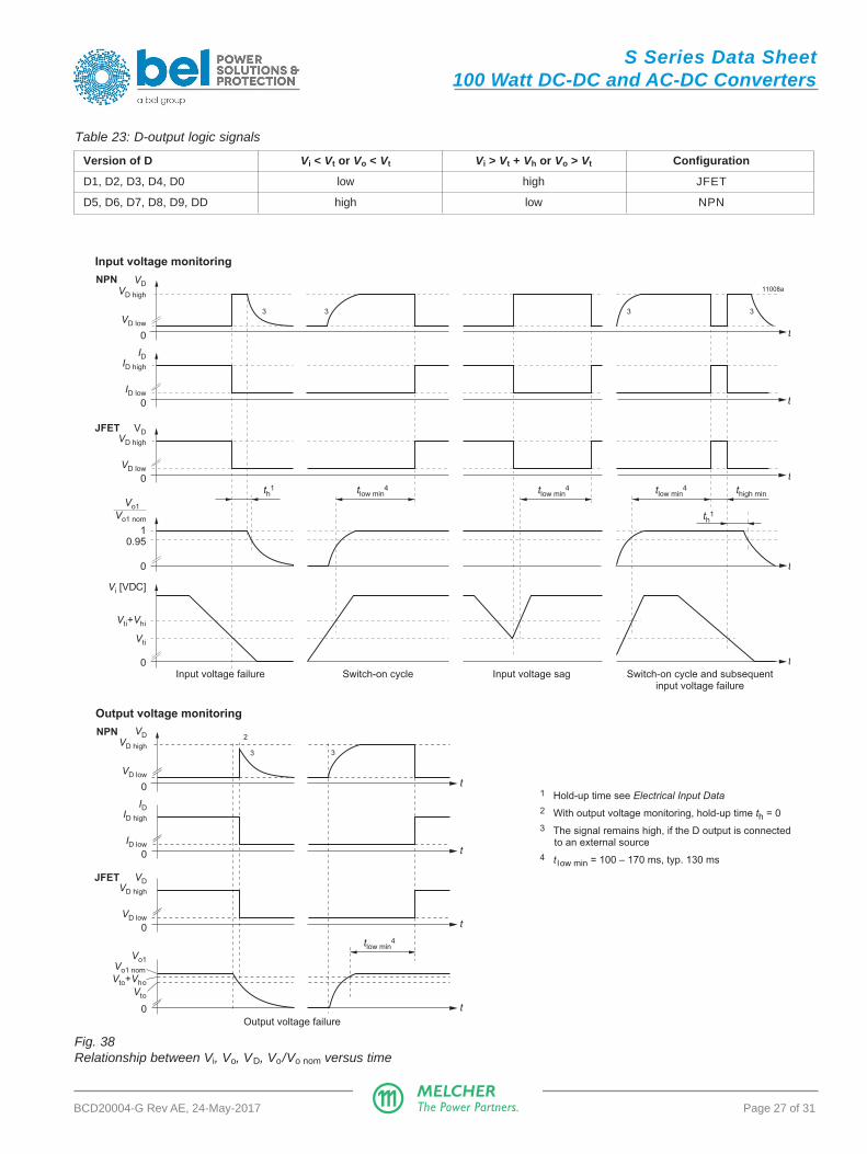
Fig. 38Relationship between Vi, Vo, VD, Vo/Vo nom versus time
Table 23: D-output logic signals
Version of D Vi < Vt or Vo < Vt Vi > Vt + Vh or Vo > Vt Configuration
D1, D2, D3, D4, D0 low high JFET
D5, D6, D7, D8, D9, DD high low NPN
0
10.95
0
Vi [VDC]
0
t
t
t
tlow min4 tlow min
4 thigh min
th1
Vti+Vhi
Vti
Input voltage failure Switch-on cycle Input voltage sag Switch-on cycle and subsequentinput voltage failure
VD high
VD low
VD
0
JFET
NPN
t
Vo1
Vo1 nom
VD high
VD low
VD
tlow min4th
1
0
0
VD high
VD low
VD
0
JFET
NPN
Vo1
VD high
VD low
VD
tlow min4
Vto
3
Output voltage failure
0
ID high
ID low
ID
t
0
ID high
ID low
ID
t
t
t
t
3
2
3 3 3 3
Vo1 nom
Vto+Vho
Input voltage monitoring
Output voltage monitoring
11008a
1 Hold-up time see Electrical Input Data
2 With output voltage monitoring, hold-up time th = 0
3 The signal remains high, if the D output is connected to an external source
4 t low min = 100 – 170 ms, typ. 130 ms

S Series Data Sheet100 Watt DC-DC and AC-DC Converters
BCD20004-G Rev AE, 24-May-2017 Page 28 of 31MELCHERThe Power Partners.
V ACFAIL signal (VME)
Available for converters with Vo nom = 5.1 V only.
This option defines an undervoltage monitoring circuit for theinput or for the input and main output voltage ( 5.1 V) similar tooption D and generates an ACFAIL signal (V signal), whichconforms to the VME standard.
The low state level of the ACFAIL signal is specified at a sinkcurrent of IV ≤ 48 mA to VV ≤ 0.6 V (open-collector output of anNPN transistor). The pull-up resistor feeding the open-collectoroutput should be placed on the VME back plane.
After the ACFAIL signal has gone low, the VME standardrequires a hold-up time t h of at least 4 ms, before the 5.1 Voutput drops to 4.875 V, when the output is fully loaded. Thishold-up time th is provided by the internal input capacitance Ci;see tab. Input Data. Consequently the working input voltageand the threshold level Vt i should be adequately above Vi min ofthe converter, so that enough energy is remaining in the inputcapacitance. If V i is below the required level, an external hold-up capacitor (Ci ext) should be added; refer to these formulas:
2 • Po • (th + 0.3 ms) • 100 Vt i = –––––––––––––––––––––––– + Vi min
2
Ci min • η
2 • Po • (th + 0.3 ms) • 100 C i ext = –––––––––––––––––––––– – Ci minη • (Vti
2 – Vi min2 )
where as:C i min = internal input capacitance [mF]; see table 2C i ext = external input capacitance [mF]Po = output power [W]η = efficiency [%]t h = hold-up time [ms]V i min = minimum input voltage [V] 1
V ti = threshold level [V]1 V i min see Electrical Input Data. For output voltages Vo > Vo nom,
V i min increases proportionally to Vo/Vo nom.
Note: Option V2 and V3 can be adjusted by the potentiometer to athreshold level between Vi min and Vi max. A decoupling diode shouldbe connected in series with the input of AS – FS converters toavoid the input capacitance being discharged through other loadsconnected to the same source voltage.
Option V operates independently of the built-in input under-voltage lockout circuit. A logic "low" signal is generated at pin20, as soon as one of the monitored voltages drops below thepreselected threshold level Vt. The return for this signal isS–. The V output recovers, when the monitored voltagesexceed Vt + Vh. The threshold level Vt i is either adjustable by apotentiometer, accessible through a hole in the front cover, oradjusted in the factory to a determined customer-specificvalue. Refer to table 25.
V output (V0, V2, V3):
Pin V is internally connected to the open collector of an NPNtransistor. The emitter is connected to S–. VV ≤ 0.6 V (logiclow) corresponds to a monitored voltage level (V i and/or Vo)<V t. IV should not exceed 50 mA. The V output is not protectedagainst external overvoltages: VV should not exceed 60 V.
Threshold tolerances and hysteresis:
If Vi is monitored, the internal input voltage is measured afterthe input filter. Consequently this voltage differs from the
Table 25: Undervoltage monitor functions
Option Monitoring Minimum adjustment range Typical hysteresis Vh [% of V t]of threshold level V t for V t min – V t max
V i Vo1 V ti Vto Vhi Vho
V2 yes no V i min – V i max 1 -- 3.4 - 0.4 --
V3 yes yes V i min – V i max 1 0.95 - 0.985 Vo1
2 3.4 - 0.4 "0"
V0 yes no V i min – V i max 3 4 -- 3.4 - 0.4 --
yes yes V i min – V i max 3 4 0.95 - 0.985 Vo1
2 3.4 - 0.4 "0"
1 Threshold level adjustable by potentiometer. 2 Fixed value between 95% and 98.5% of Vo1 (tracking). 3 Adjusted at Io nom.4 Fixed value, resistor-adjusted (±2% at 25°C) accord. to customer's specification; individual type number is determined by the company..
Table 24: Option V: Factory potentiometer setting of Vt i with resulting hold-up time
Model AS B S F S CS D S E S LS Unit
Vt i 9.5 19.5 39 39 61 97 120 VDC
t h 0.1 0.1 3.4 1.1 1.1 2.7 4.2 ms
Table 26: NPN-output (V0, V2, V3)
Vi, Vo status V output, VV
V i or Vo1 < V t low, L, VV ≤ 0.6 V at IV = 50 mA
V i and Vo1 > V t + Vh high, H, IV ≤ 25 µA at VV = 5.1 V
voltage at the connector pins by the voltage drop ∆V ti acrossthe input filter. The threshold level of option V0 is adjusted in thefactury at Io nom and TA = 25 °C. The value of ∆V ti depends uponthe input voltage range (AK, BK, etc.), threshold level V t,temperature, and input current. The input current is a functionof input voltage and output power.

S Series Data Sheet100 Watt DC-DC and AC-DC Converters
BCD20004-G Rev AE, 24-May-2017 Page 29 of 31MELCHERThe Power Partners.
3
5.1 V4.875 V
0
Vi [VDC]
0
t
t
Vti + Vhi
Vti
Input voltage failure Switch-on cycle Input voltage sag Switch-on cycle and subsequentinput voltage failure
VV high
VV low
VV
0
V2
t
Vo
0
VV high
VV low
VV
0
V2
Vi
Vti
4
Output voltage failure
0
VV high
VV low
VV
3
Vti + Vhi
tlow min 2 tlow min
2tlow min 2
3 3
44
VV high
VV low
VV
0
V3
t
3
tlow min 2tlow min
2
3 3
th 1
2.0 V
th 1
4
3
4
tlow min 2
V3
5.1 V4.875 V
0
Vo
2.0 V
Input voltage monitoring
Output voltage monitoring
11010a
t
t
t
t
∆Vti Vhi
VV low
VV
VV high
Vi
Po =
Po
no
m
Po =
0
Po =
0
Vti
Po =
Po
no
m
11023a
Fig. 40Output configuration of options V0, V2 and V3
Fig. 41Definition of Vti, ∆Vti and Vhi
1 VME request: minimum 4 ms2 t low min = 40 – 200 ms, typ 80 ms3 VV level not defined at Vo < 2.0 V4 The V signal drops simultaneously with Vo, if the pull-up
resistor R P is connected to Vo+; the V signal remainshigh if RP is connected to an external source.
Fig. 39Relationship between Vb, Vo, VD, Vo /Vo nom versus time
Vo+
S–
V
VV
IVRp
Inp
ut
11009a
NPN open
collector
20
14
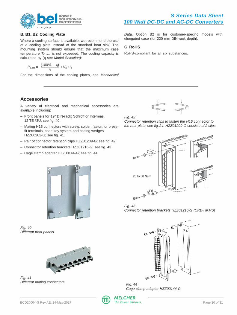
S Series Data Sheet100 Watt DC-DC and AC-DC Converters
BCD20004-G Rev AE, 24-May-2017 Page 30 of 31MELCHERThe Power Partners.
Data. Option B2 is for customer-specific models withelongated case (for 220 mm DIN-rack depth).
G RoHS
RoHS-compliant for all six substances.
B, B1, B2 Cooling Plate
Where a cooling surface is available, we recommend the useof a cooling plate instead of the standard heat sink. Themounting system should ensure that the maximum casetemperature TC max is not exceeded. The cooling capacity iscalculated by (η see Model Selection):
(100% – η)PLoss = –––––––––– • Vo • Ioη
For the dimensions of the cooling plates, see Mechanical
Fig. 44Cage clamp adapter HZZ00144-G
AccessoriesA variety of electrical and mechanical accessories areavailable including:
– Front panels for 19" DIN-rack: Schroff or Intermas,12 TE /3U; see fig. 40.
– Mating H15 connectors with screw, solder, faston, or press-fit terminals, code key system and coding wedgesHZZ00202-G; see fig. 41.
– Pair of connector retention clips HZZ01209-G; see fig. 42
– Connector retention brackets HZZ01216-G; see fig. 43
– Cage clamp adapter HZZ00144-G; see fig. 44
Fig. 40Different front panels
Fig. 41Different mating connectors
Fig. 42Connector retention clips to fasten the H15 connector tothe rear plate; see fig. 24. HZZ01209-G consists of 2 clips.
Fig. 43Connector retention brackets HZZ01216-G (CRB-HKMS)
20 to 30 Ncm
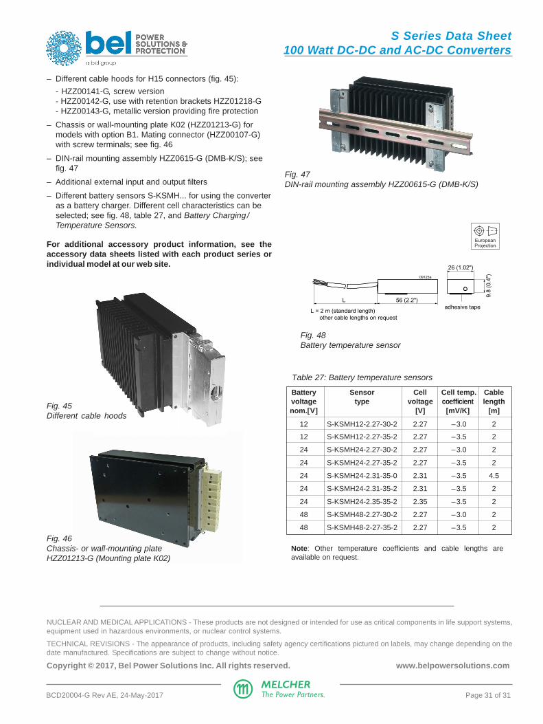
S Series Data Sheet100 Watt DC-DC and AC-DC Converters
BCD20004-G Rev AE, 24-May-2017 Page 31 of 31MELCHERThe Power Partners.
Fig. 46Chassis- or wall-mounting plateHZZ01213-G (Mounting plate K02)
Fig. 47DIN-rail mounting assembly HZZ00615-G (DMB-K/S)
– Different cable hoods for H15 connectors (fig. 45):
- HZZ00141-G, screw version- HZZ00142-G, use with retention brackets HZZ01218-G- HZZ00143-G, metallic version providing fire protection
– Chassis or wall-mounting plate K02 (HZZ01213-G) formodels with option B1. Mating connector (HZZ00107-G)with screw terminals; see fig. 46
– DIN-rail mounting assembly HZZ0615-G (DMB-K/S); seefig. 47
– Additional external input and output filters
– Different battery sensors S-KSMH... for using the converteras a battery charger. Different cell characteristics can beselected; see fig. 48, table 27, and Battery Charging /Temperature Sensors.
For additional accessory product information, see theaccessory data sheets listed with each product series orindividual model at our web site.
Fig. 45Different cable hoods
56 (2.2")L
L = 2 m (standard length) other cable lengths on request
adhesive tape
26 (1.02")
9.8
(0.4
")09125a
EuropeanProjection
Table 27: Battery temperature sensors
Battery Sensor Cell Cell temp. Cablevoltage type voltage coefficient lengthnom. [V] [V] [mV/K] [m]
12 S-KSMH12-2.27-30-2 2.27 –3.0 2
12 S-KSMH12-2.27-35-2 2.27 –3.5 2
24 S-KSMH24-2.27-30-2 2.27 –3.0 2
24 S-KSMH24-2.27-35-2 2.27 –3.5 2
24 S-KSMH24-2.31-35-0 2.31 –3.5 4.5
24 S-KSMH24-2.31-35-2 2.31 –3.5 2
24 S-KSMH24-2.35-35-2 2.35 –3.5 2
48 S-KSMH48-2.27-30-2 2.27 –3.0 2
48 S-KSMH48-2-27-35-2 2.27 –3.5 2
Fig. 48Battery temperature sensor
Note: Other temperature coefficients and cable lengths areavailable on request.
NUCLEAR AND MEDICAL APPLICATIONS - These products are not designed or intended for use as critical components in life support systems,equipment used in hazardous environments, or nuclear control systems.
TECHNICAL REVISIONS - The appearance of products, including safety agency certifications pictured on labels, may change depending on thedate manufactured. Specifications are subject to change without notice.
Copyright © 2017, Bel Power Solutions Inc. All rights reserved. www.belpowersolutions.com