S INGLE -B ALANCED M IXER P ROJECT D ESIGN R EVIEW RIT Senior Project Jared Burdick Held May 3, 2012...
24
SINGLE-BALANCED MIXER PROJECT DESIGN REVIEW RIT Senior Project Jared Burdick Held May 3, 2012 Updated May 5, 2012 with Action Items
-
Upload
percival-brooks -
Category
Documents
-
view
214 -
download
0
Transcript of S INGLE -B ALANCED M IXER P ROJECT D ESIGN R EVIEW RIT Senior Project Jared Burdick Held May 3, 2012...

SINGLE-BALANCED MIXER PROJECT
DESIGN REVIEW
RIT Senior Project
Jared Burdick
Held May 3, 2012
Updated May 5, 2012 with Action Items

AGENDA
Schedule Specifications Block diagram Components used Design decisions / trade-offs AWR model Simulation results Circuit layout Fabrication / assembly Testing Action Items & Notes from Review
SCHEDULE
Key Milestones Concept Design selections Model build / simulation Design review Fabricate circuit & mixer
assembly Test assembly Evaluate results Write report Demonstration at RIT
Completion Date March 23 April 13 April 26 May 3 May 11
May14 May 16 May 21 TBD

SPECIFICATIONS
Spec # Function Specification (metric)Unit of
MeasureMarginal
ValueComments
S1 1 RF Frequency GHz 0.8 - 1.2 RF Input frequency range.S2 2 LO Frequency GHz 1 LO frequency (fixed).S3 7 IF Frequency MHz DC - 200 IF output frequency range.
S4 1,7 Conversion Loss dB 10Difference in power between signal entering RF port and output IF port.
S5 1,2,4,5 RF/IF Isolation dB 30 Relative to the RF InputS6 2,4,5,7 LO/IF Isolation dB 35 Relative to the LO Input Power
S7 2 Minimum LO Power dBm 10Minimum LO power level required for all other specs to be met.
S8 1 Maximum RF Power dBm -10Maximum RF power level required for all other specs to be met.
S9 1,7 1dB Compression dBm 15The input RF power level at which conversion loss increases by 1 dB.
S10 1,2,5,8 RF VSWR Ratio 2.0:1VSWR to be measured with LO power at 10 dBm.
S11 2,5,8 LO VSWR Ratio 2.5:1Should have same performance as RF port
S12 2,5,6,7,8,10 IF VSWR Ratio 1.5:1VSWR to be measured with LO power at 10 dBm.

BLOCK DIAGRAM
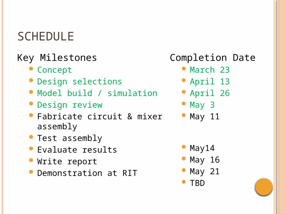
COMPONENT LIST RF splitting (1)
Anaren SMD Hybrid Coupler Diodes (2)
Avago RF Schottky-barrier series pair (1) LPF (1)
Lumped element maximally flat – 5th order RF connectors (3)
SMA female jack end-launch printed circuit board mount Printed circuit functions (on RO4003, 32-mil thick, 1oz.
copper) RF chokes – shorted λ/4 stub (2) Impedance transformer - λ/4 (1) 50Ω lines (5)
SUBSTRATE MATERIAL

HYBRID COUPLER
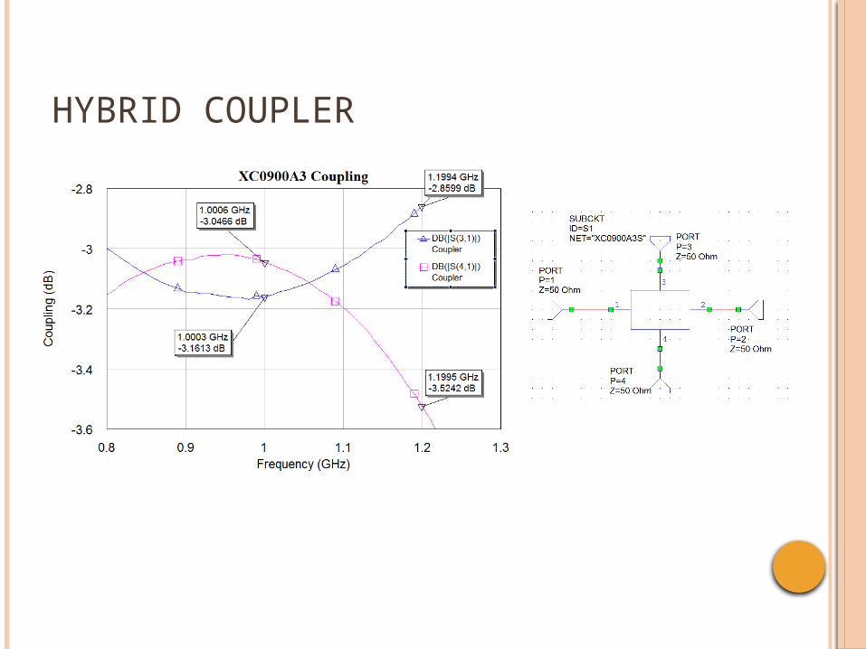
HYBRID COUPLER
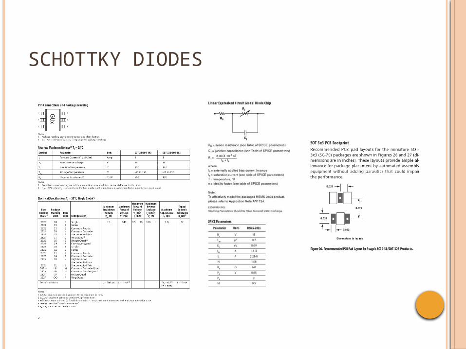
SCHOTTKY DIODES

LOW-PASS FILTER

SMA CONNECTORS

PRINTED LINE CONSIDERATIONS RF chokes
Maximized line width vs. performance to gain production margin (narrow line-widths more difficult to produce).
Need to stub is well grounded – brought it close to the edge where a strap can be installed.
Quarter-wave impedance transformer Meandered to minimize the size of the circuit substrate. Tapered the line where it met component pads. Mitered corners.
50Ω interconnects Mitered corners.
Grounding Added ground to the top of the circuit board wherever possible to reduce impedance. Will connect top & and bottom planes with wires and straps. This would normally be
accomplished with plated via’s.
Component pads Used manufacturers’ recommendations.

DESIGN DECISIONS MADE / TRADE-OFFS
RF Splitting Looked at 90, 180 degree couplers. 90-degree easier to implement. Surface mount standard product readily available from Anaren
(distribution) & inexpensive. Greatly simplifies the circuit board.
Filtering Removed BPF’s in the RF and LO paths
Not readily available or too expensive. Not enough time to design lumped-element realizations. Not critical to performance or meeting specification.
LPF (IF path) Maximally flat – desire good pass-band flatness and suppress the 1.0 GHz LO
leakage. Lumped-element – distributed too large, components are inexpensive. 5th order (see design and simulation later). Purchase coils, use DLI capacitors.

DECISIONS / TRADE-OFFS RF Chokes
Started with radial transformers (λ/2 open stubs). Did not simulate very well – higher conversion loss & poor flatness.
Moved to λ/4 shorted stubs (high impedance). Diodes
Avago Schottky series pair diodes selected. Using a pair improve diode match (to each other). Also purchased Infineon pair as a risk reduction (same package so they can
be installed on existing circuit). Substrate Material
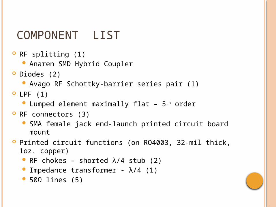
Rogers RO4003 selected. Low-cost microwave material. FR-4 could potentially be utilized – risk item (higher loss, more εr variation) 32-mil thickness selected to provide some rigidity for the soldered
components and the connectors. 1-oz copper used due to soldering, particularly the connectors – fear that
0.5 oz would tear or lift during hand-solder operations.
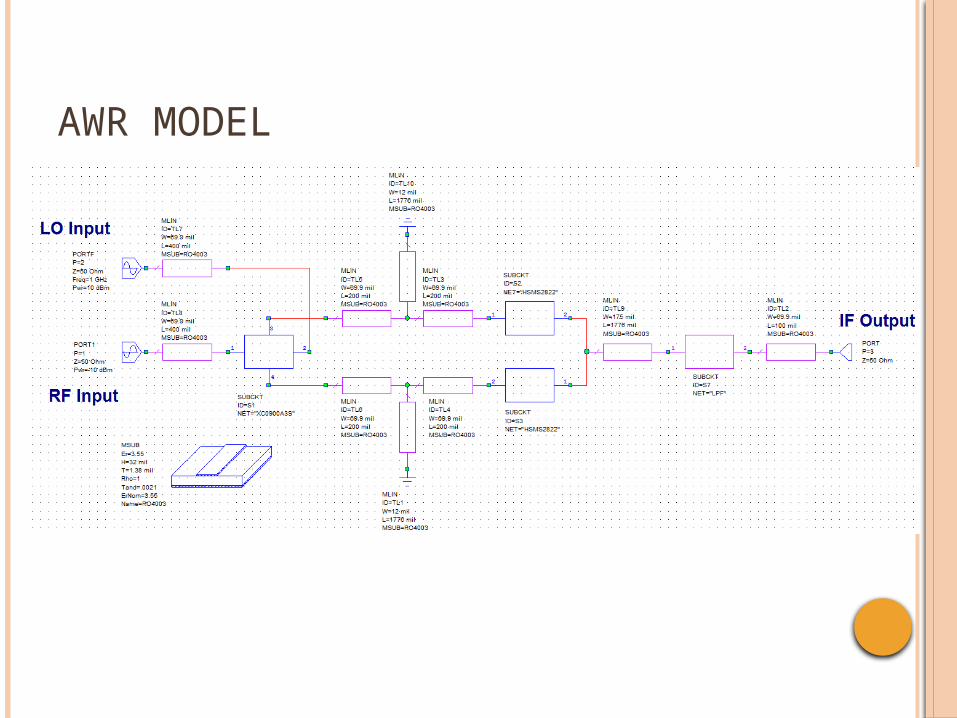
AWR MODEL

SIMULATION RESULTS

SIMULATION RESULTS
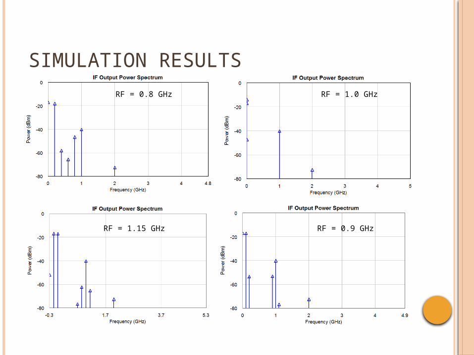
SIMULATION RESULTS
RF = 1.0 GHzRF = 0.8 GHz
RF = 0.9 GHzRF = 1.15 GHz
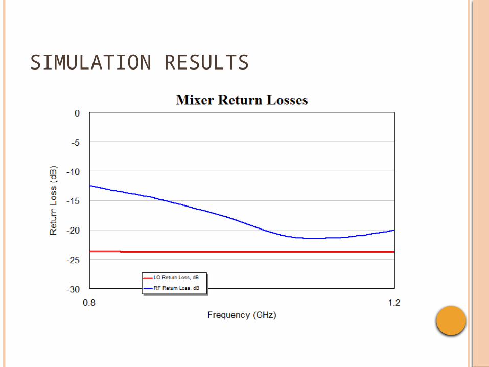
SIMULATION RESULTS
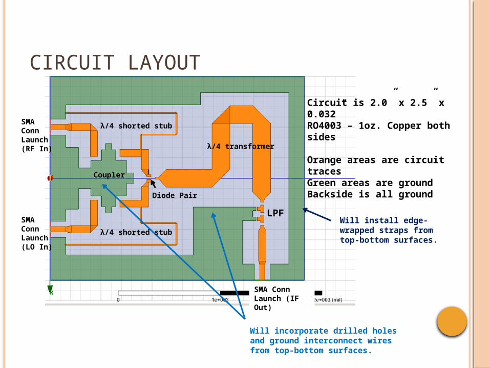
CIRCUIT LAYOUT
Circuit is 2.0” x 2.5” x 0.032”RO4003 – 1oz. Copper both sides
Orange areas are circuit tracesGreen areas are groundBackside is all ground
Will incorporate drilled holes and ground interconnect wires from top-bottom surfaces.
Will install edge-wrapped straps from top-bottom surfaces.
SMA Conn Launch(RF In)
SMA Conn Launch(LO In)
SMA Conn Launch (IF Out)
LPF
λ/4 transformer
Diode Pair
Coupler
λ/4 shorted stub
λ/4 shorted stub

FABRICATION & ASSEMBLY Circuit to be fabricated at Anaren using LPKF prototype circuit
router. Approximately 4 circuits will be produced initially – more if needed. Will require some hand de-burring of copper. Inside corners will not be 90-degrees, there will be a small radius base on
the diameter of the end-mill used. The small gap for the LPF shunt capacitors may have to be hand cut with a
scalpel. Circuit assembly will be performed by Anaren Assembly Technician
Basic soldering of components using manufacturer’s recommendations where possible (recommended footprints were incorporated in the design/layout).
Manual soldering of ground connections from top to bottom copper layers using:
Edge-wraps Wires through drilled holes.
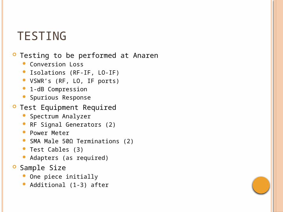
TESTING Testing to be performed at Anaren
Conversion Loss Isolations (RF-IF, LO-IF) VSWR’s (RF, LO, IF ports) 1-dB Compression Spurious Response
Test Equipment Required Spectrum Analyzer RF Signal Generators (2) Power Meter SMA Male 50Ω Terminations (2) Test Cables (3) Adapters (as required)
Sample Size One piece initially Additional (1-3) after

ACTION ITEMS & NOTES FROM REVIEW
Action Items & Notes from SBM Design Review Held 5/3/2012
Note No.
Description Owner Due Date Status Comments/Updates
1Question on LO and RF connector spacing - enough for getting connectors on.
Jared 5/4/2012 Closed Spacing was determined to be suffi cient as is
2 Possibility of Breadboarding the LPF by itself. Jared See Below Closed This can be easily done if needed
3 Potential for NF testing Jared See Below Open Not required, but desired.
4 Question on measuring LO to RF Isolation Jared 5/3/2012 ClosedIt was agreed that LO-RF isolation will be poor due to the configuration and did not need to be measured.
5 Bandpass Filtering on RF & LO ports Jared 5/3/2012 ClosedThis would be added to the production version - it was left out due to diffi culty in obtaining in time (beyond scope of project).
6An RF Bypass capacitor between the diodes and the impedance transformer should improve conversion loss performance.
Jared See Below Closed See Below.
Action Item No.
Description Owner Due Date Status Comments/Updates
1 Evaluate adding RF Bypass capacitor Jared 5/5/2012 ClosedA 2.7 pF capacitor was added to the AWR model and the performance did improve. This was added to the design.
2 Breadboard the LPF Jared TBD Open Will do if required.
3 Investigate possibility of adding NF testing. Jared 5/9/2012 OpenNeed to check with Anaren if equipment is available.