S COMM 903 Lecture #6eee.guc.edu.eg/Courses/Communications/COMM903... · GUC (Dr. Hany Hammad)...
13
GUC (Dr. Hany Hammad) 10/24/2016 COMM 903 Lecture #6 1 © Dr. Hany Hammad, German University in Cairo Lecture # 6 Contents • Microwave Amplifier Design. – Two port power gains. – Stability. – Stability Circles. – Tests for unconditional stability. – Single-Stage Transistor Amplifier Design. – Constant gain circles and design for specified gain. – Low noise amplifier design. © Dr. Hany Hammad, German University in Cairo Single-Stage Transistor Amplifier Design * 22 21 12 11 1 s L L in S S S S * 11 21 12 22 1 L S S out S S S S * s in * L out s L L S S S S * * 22 * * 21 * 12 * 11 1 * 11 21 12 11 22 1 1 L S S S S S S S S * * 22 * * 21 * 12 * * 22 * 11 1 1 L s L L S S S S S S S S S S S S S S S S S S S S S S S S S S S S 11 21 12 * 21 * 12 11 22 * 21 * 12 11 * 22 21 12 11 22 * 22 * 11 1 1 1 1 1 S S S s S S S S S S S 11 21 12 * 22 11 22 * 22 1 1 1 S S S S S S S S S S S S S S S S S S S S S 21 12 * 21 * 12 11 22 * 21 * 12 * 22 21 12 11 22 * 22 11 * 11 1 1 1 S S S s S S S S S S S 21 12 * 22 11 22 * 22 11 1 1 • To achieve maximum power transfer
Transcript of S COMM 903 Lecture #6eee.guc.edu.eg/Courses/Communications/COMM903... · GUC (Dr. Hany Hammad)...

GUC (Dr. Hany Hammad) 10/24/2016
COMM 903 Lecture #6 1
© Dr. Hany Hammad, German University in Cairo
Lecture # 6 Contents
• Microwave Amplifier Design.
– Two port power gains.
– Stability.
– Stability Circles.
– Tests for unconditional stability.
– Single-Stage Transistor Amplifier Design.
– Constant gain circles and design for specified gain.
– Low noise amplifier design.
© Dr. Hany Hammad, German University in Cairo
Single-Stage Transistor Amplifier Design
*
22
211211
1s
L
Lin
S
SSS
*
11
211222
1L
S
Sout
S
SSS
*
sin *
Lout
s
L
L
S
SSS
**
22
**
21
*
12*
111
*
11
21121122
1
1L
S
SS
S
SSSS
**
22
**
21
*
12
**
22
*
11 11 LsLL SSSSS
S
SS
S
SS
S
SSSSSSSS
S
SSSSSSS
11
2112
*
21
*
121122
*
21
*
12
11
*
2221121122
*
22*
111
1
1
11
S
SSs
S
SSSSSS
11
2112
*
221122
*
22
1
11
SSSSS SSSSSSSSSSSSSSSS 2112
*
21
*
121122
*
21
*
12
*
2221121122
*
2211
*
11 111
SSSs SSSSSSS 2112
*
221122
*
2211 11
• To achieve maximum power transfer

GUC (Dr. Hany Hammad) 10/24/2016
COMM 903 Lecture #6 2
© Dr. Hany Hammad, German University in Cairo
Single-Stage Transistor Amplifier Design
SSSSS SSSSSSSSSSSSSSSS 2112
*
21
*
121122
*
21
*
12
*
2221121122
*
2211
*
11 111
SSSs SSSSSSS 2112
*
221122
*
2211 11
2112
*
222211
*
2211
2 SSSSSSSs
22
*
222112
*
21
*
122211
*
21
*
12
*
22
*
11211222
*
22
*
1111
*
1111 1 SSSSSSSSSSSSSSSSSSSSS
0
*
22112112
*
222211
*
2211 SSSSSSSSSa
Note
**
22
*
1122
*
21
*
1222
*
22
*
11
*
11 ASSSSSSSSSc
2
s
1
s
a
b
22
*
21
*
1222
*
22
*
11
*
11 SSSSSSS
c
22
22
2
111 SSb
0
s
1
2
1
2
11
2
4
C
CBBSM
22
22
2
111 1 SSbB
*
22111 SSaC
02 cbxax
© Dr. Hany Hammad, German University in Cairo
Single-Stage Transistor Amplifier Design
2
2
2
2
22
2
4
C
CBBLM
Similarly Solving for L
22
11
2
222 1 SSB
*
11222 SSC

GUC (Dr. Hany Hammad) 10/24/2016
COMM 903 Lecture #6 3
© Dr. Hany Hammad, German University in Cairo
Single-Stage Transistor Amplifier Design
*
Sin *
Lout
2
22
2
2
212
2
1
1
1
1max
L
L
Sin
S
T
SSG
2
22
2
2
212*
2
1
1
1
1
L
L
SS
S
SS
2
22
2
2
2121
1
1
1max
L
L
S
T
SSG
)1( 2
12
21
max KK
S
SGT
(only used when K>1)
1
2
1
2
11
2
4
C
CBBSM
2
2
2
2
22
2
4
C
CBBLM
&
*
11222
*
22111
22
11
2
222
22
22
2
111
1
1
SSC
SSC
SSB
SSB
© Dr. Hany Hammad, German University in Cairo
Single-Stage Transistor Amplifier Design
For a unilateral case 012 S
11
22
211211
*
1S
S
SSS
L
LSin
22
22
211222
*
1S
S
SSS
S
SLout
2
22
2
212
11 1
1
1
1max
SS
SGTU
)1( 2
12
21
max KK
S
SGT
When K=1
12
21
S
SGmsg Maximum Stable Gain
=1 =1
GUC (Dr. Hany Hammad) 10/24/2016
COMM 903 Lecture #6 4
© Dr. Hany Hammad, German University in Cairo
Example
Design an amplifier for maximum gain at 4 GHz. Calculate and plot the input return loss and the gain from 3 to 5 GHz. The GaAs FET has the following S parameters (Zo=50 )
)(GHzf11S 21S 12S 22S
0.3
0.4
0.5
o8980.0 o11672.0 o14266.0
o9986.2 o7660.2 o5439.2
o5603.0 o5703.0 o6203.0
o4176.0 o5473.0 o6872.0
Solution:
Check the stability of the transistor by calculating and K at GHz
oSSSS 162488.021122211
195.12
1
2112
22
22
2
11
SS
SSK
1
1K
Unconditionally Stable at 4.0 GHz
We can design for conjugate matching
© Dr. Hany Hammad, German University in Cairo
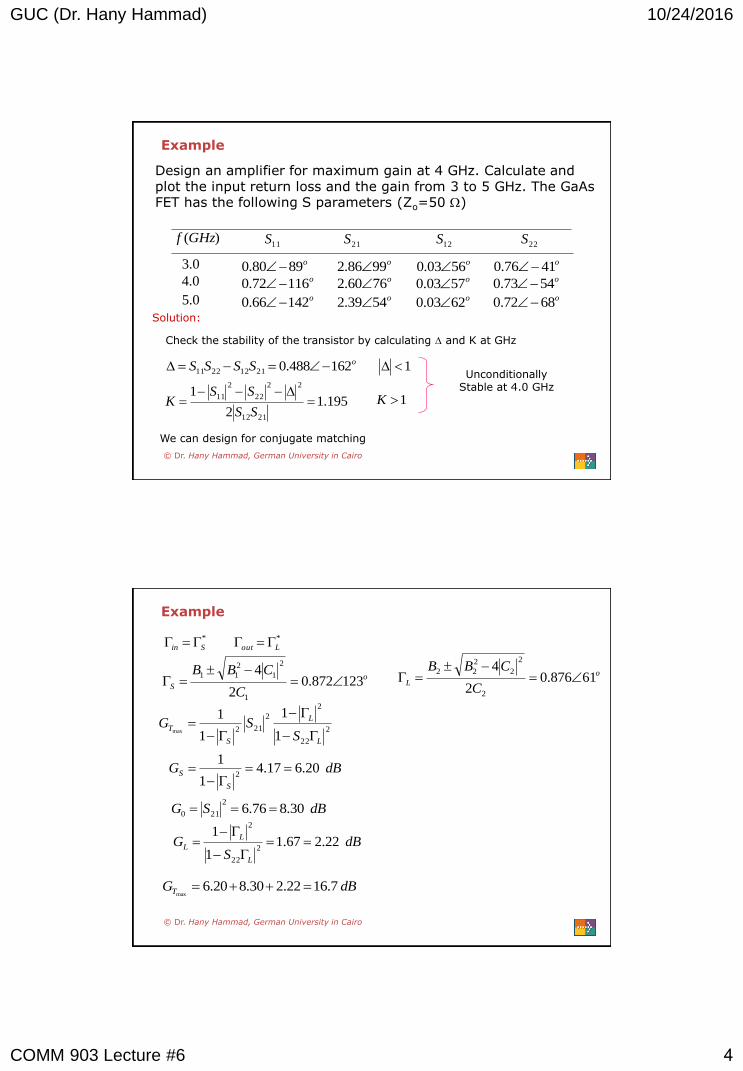
Example
o
SC
CBB123872.0
2
4
1
2
1
2
11
o
LC
CBB61876.0
2
4
2
2
2
2
22
*
Sin *
Lout
2
22
2
2
2121
1
1
1max
L
L
S
T
SSG
dBG
S
S 20.617.41
12
dBSG 30.876.62
210
dBS
G
L
L
L 22.267.11
12
22
2
dBGT 7.1622.230.820.6max

GUC (Dr. Hany Hammad) 10/24/2016
COMM 903 Lecture #6 5
© Dr. Hany Hammad, German University in Cairo
Example
© Dr. Hany Hammad, German University in Cairo
Example

GUC (Dr. Hany Hammad) 10/24/2016
COMM 903 Lecture #6 6
© Dr. Hany Hammad, German University in Cairo
Constant gain circles and design for specified gain
• To improve bandwidth one should design for a gain less than the maximum obtainable gain.
• Impedance mismatches are purposely introduced to reduce the maximum gains.
• This can be done by plotting constant gain circles on smith chart to represent loci of s and L that give fixed values of gain for the input and output sections (Gs and GL).
• For simplicity consider the unilateral case (S12 is very small)
22
1
1
1
1
UG
G
U TU
T
2
22
2
11
22211211
11 SS
SSSSU
(unilateral figure of merit)
An error of a few tenths of a dB or less will justify the unilateral assumption
© Dr. Hany Hammad, German University in Cairo
Constant gain circles and design for specified gain
2
22
2
11
222
21
11
11
LS
LS
TU
SS
SG
2
11
2
1
1
S
S
S
SG
2
21SGo 2
22
2
1
1
L
L
L
SG
*
11SS *
22SL
2
11
22
11
2
11
max
1
1
1
1
SS
SGS
2
22
max
1
1
SGL
Gain is maximized when
2
112
11
2
max
11
1S
SG
Gg
S
S
S
Ss
2
222
22
2
max
11
1S
SG
Gg
L
L
L
LL
Normalized gain factors
10 sg
10 Lg
Range
&

GUC (Dr. Hany Hammad) 10/24/2016
COMM 903 Lecture #6 7
© Dr. Hany Hammad, German University in Cairo
Constant gain circles and design for specified gain
For a fixed value of gs or gl we need to plot the gain circles
2
11
22
11 111 SSg SSs
2
11
2**
1111 1111 SSSg SSSs
2
11
22
11
222
11
**
1111 1 SSSgSgSgg SSSsSsSss
sSSssS gSSSgSSg 2
11
**
1111
2
11
2
11
211
2
11
2
11
2
11
**
11112
11
1
11 Sg
gS
Sg
SSg
s
s
s
SSsS
2
2
11
2
11
2
11
Sg
Sg
s
SAdd to both sides
© Dr. Hany Hammad, German University in Cairo
Constant gain circles and design for specified gain
2
2
11
2
11
2
2
11
2
11
2
2
11
2
11
2
2
11
**
11112
1111
1
1111
Sg
Sg
Sg
gS
Sg
Sg
Sg
SSg
s
S
s
s
s
S
s
SSsS
2
11
2
11
22
11
2
11
2
2
11
*
11
11
111
11 Sg
SgSggS
Sg
Sg
s
Sss
s
sS
2
11
2
11
2
11
*
11
11
11
11 Sg
Sg
Sg
Sg
s
s
s
sS
2
11
*
11
11 Sg
SgC
s
sS
2
11
2
11
11
11
Sg
SgR
s
s
S
Similarly
2
22
*
22
11 Sg
SgC
L
LL
2
22
2
22
11
11
Sg
SgR
L
L
L

GUC (Dr. Hany Hammad) 10/24/2016
COMM 903 Lecture #6 8
© Dr. Hany Hammad, German University in Cairo
Constant gain circles and design for specified gain
If
2
11
2
11
11
11
Sg
SgR
s
s
S
)0( 1 dBGs
2
11
*
11
11 Sg
SgC
s
sS
2
112
11max
111
1S
SG
Gg
S
Ss
4
11
*
11
2
11
2
11
2
11
*
11
2
11
1
1
111
1
S
SS
SS
SSCS
2
11
*
11
1 S
S
2
11
2
11
2
11
2
11
111
111
SS
SSRS
4
11
2
11
2
11
1
1
S
SS
2
11
11
1 S
S
The gain circle will always pass through Smith Chart
© Dr. Hany Hammad, German University in Cairo
Example
Design an amplifier to have a gain of 11 dB at 4.0 GHz. Plot the constant gain circles for Gs=2 dB and 3 dB, and GL = 0 dB and 1 dB. Calculate and plot the input return loss and overall amplifier gain from 3 to 5 GHz. Use an FET with the following S parameters (Zo= 50 ).
)(GHzf 11S 21S 12S22S
3
4
5
o908.0 o12075.0 o14071.0
o1008.2 o805.2 o603.2
0 o5066.0
0 o7060.0
0 o8558.0
Solution
012 Ssince Unilateral Case 111 S 122 S & Unconditionally Stable
dBS
GS 6.329.21
12
11
max
dBS
GL 9.156.11
12
22
max
dBSG 0.825.62
210
GUC (Dr. Hany Hammad) 10/24/2016
COMM 903 Lecture #6 9
© Dr. Hany Hammad, German University in Cairo
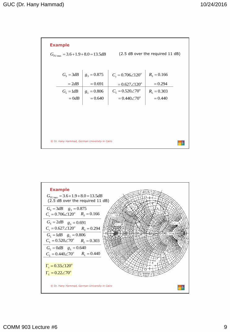
Example
dBGTU 5.130.89.16.3max (2.5 dB over the required 11 dB)
dBGS 3
dB2
dBGL 1
dB0
875.0Sg
691.0
806.0Lg
640.0
o
sC 120706.0
o120627.0 o
LC 70520.0
o70440.0
166.0SR
294.0
303.0LR
440.0
© Dr. Hany Hammad, German University in Cairo
Example
dBGTU 5.130.89.16.3max (2.5 dB over the required 11 dB)
o
s 12033.0
o
L 7022.0
dBGS 3
dBGS 2
dBGL 1
dBGL 0
875.0Sg
691.0Sg
806.0Lg
640.0Lg
o
sC 120706.0
o
sC 120627.0
o
LC 70520.0
o
LC 70440.0
166.0SR
294.0SR
303.0LR
440.0LR

GUC (Dr. Hany Hammad) 10/24/2016
COMM 903 Lecture #6 10
© Dr. Hany Hammad, German University in Cairo
Example
© Dr. Hany Hammad, German University in Cairo
Low-Noise Amplifier Design
• In receiver applications it is often required to have a preamplifier with a low noise figure as possible since the first stage of a receiver front end usually has the dominant effect on the noise performance of the overall system.
• It is not possible to obtain both minimum noise figure and maximum gain for an amplifier, a compromise must be made.
• This can be done by using constant gain circles and circles of constant noise figure to select a usable trade-off between noise figure and gain.

GUC (Dr. Hany Hammad) 10/24/2016
COMM 903 Lecture #6 11
© Dr. Hany Hammad, German University in Cairo
Low-Noise Amplifier Design
2
min opts
s
N YYG
RFF
sss jBGY = source admittance presented to transistor.
optY = optimum source admittance that results in minimum noise figure.
minF = minimum noise figure of transistor, obtained when Ys=Yopt
NR = equivalent noise resistance of transistor.
SG = real part of source admittance
s
s
o
sZ
Y
1
11
opt
opt
o
optZ
Y
1
11
Nopt RF ,,min are characteristics of the particular transistor being used, and are called the noise parameters of the device. They are either given by manufacturer, or measured.
© Dr. Hany Hammad, German University in Cairo
Low-Noise Amplifier Design
22
2
2
0
2
2
0
2
11
111
1
1
1
11
opts
optsoptsoptsopts
opt
opt
s
sopts
ZZYY
22
2
2
0
2
11
4
opts
opts
optsZ
YY
*
*
1
1
1
1
2
1
1
11ReRe
s
s
s
s
os
s
o
sSZZ
YG
Subtract the conjugate and divide by 2
xz
jyxjyxz
zzz
Re
2Re
2Re
**
*
2
2
0 1
11
s
s
SZ
G
22
2
min
11
4
opts
opts
o
N
Z
RFF
Let N is the noise figure parameter
2
2
1 s
optsN

GUC (Dr. Hany Hammad) 10/24/2016
COMM 903 Lecture #6 12
© Dr. Hany Hammad, German University in Cairo
Low-Noise Amplifier Design
2min 1
4opt
oN ZR
FFN
22
1 sopts N
2** 1 soptsopts N
22**2
soptoptsoptss NN
2**2
1 optoptsoptss NN
11
2**
2
N
N
N
optoptsopts
s
2
22
2
2**
2
1111
NN
N
NN
optoptoptoptsopts
s
1
1
1
2
N
NN
N
optopt
s
1
NC
opt
F
1
12
N
NNR
opt
F
© Dr. Hany Hammad, German University in Cairo
Example
A GaAs FET is biased for minimum noise figure and has the following S-parameters and noise parameters at 4 GHz (Z0=50 ); S11=0.6/-60o,
S12=0.05/26o, S21=1.9/81o, S22=0.5/-60o; Fmin=1.6 dB, opt=0.62/100o, RN=20 . For design purposes, assume the device is unilateral, and calculate the maximum error in GT resulting from this assumption. Then design an amplifier having a 2.0 dB noise figure with the maximum gain that is possible with this noise figure.
Solution
130.1891.0 TU
T
G
G
059.0
112
22
2
11
22211211
SS
SSSSU
dBGG TUT 53.050.0 (acceptable)
0986.010062.01)50()20(4
445.158.11
4
22min
o
opt
oN ZR
FFN

GUC (Dr. Hany Hammad) 10/24/2016
COMM 903 Lecture #6 13
© Dr. Hany Hammad, German University in Cairo
Example
oopt
FN
C 10056.01
24.0
1
12
N
NNR
opt
F
dBF 6.1min o
opts 10062.0
dBGS
5.10.1
7.1
Sg
805.0904.0946.0
SCo6052.0
o6058.0
o6056.0
SR
300.0205.0150.0
dBGS 7.1 (intersects the noise figure F = 2 dB circle)
o
S 7553.0 dBGS 7.1 dBF 0.2
o
L S 605.0*
22 dBS
GL 25.133.11
12
22