S-8239A Series BATTERY PROTECTION IC - · PDF fileOVERCURRENT MONITORING IC FOR...
30
S-8239A Series www.ablicinc.com OVERCURRENT MONITORING IC FOR MULTI-SERIAL-CELL PACK © ABLIC Inc., 2013-2016 Rev.1.4_04 1 The S-8239A Series is an overcurrent monitoring IC for multi-serial-cell pack including high-accuracy voltage detection circuits and delay circuits. The S-8239A Series is suitable for protection of lithium-ion / lithium polymer rechargeable battery packs from overcurrent. Features Built-in high-accuracy voltage detection circuit Overcurrent 1 detection voltage *1 0.04 V to 0.30 V (10 mV step) Accuracy 15 mV Overcurrent 2 detection voltage 0.1 V to 0.7 V (100 mV step) Accuracy 100 mV Overcurrent 3 detection voltage 1.2 V (Fixed) Accuracy 300 mV Built-in three-step overcurrent detection circuit: Overcurrent 1, overcurrent 2, overcurrent 3 Overcurrent 3 detection function is selectable: Available, unavailable UVLO (under voltage lock out) function UVLO detection voltage 2.0 V (Fixed) Accuracy 100 mV High-withstand voltage: VM pin, DO pin: Absolute maximum rating 28 V Delay times are generated only by an internal circuit (External capacitors are unnecessary). Low current consumption During normal operation: 7.0 A max. During UVLO operation: 6.0 A max. Output logic: Active "L", Active "H" Wide operation temperature range: Ta = 40C to 85C Lead-free (Sn 100%), halogen-free *1. Overcurrent 1 detection voltage 0.06 V should be satisfied in the case of overcurrent 2 detection voltage = 0.1 V. Overcurrent 1 detection voltage 0.85 overcurrent 2 detection voltage 0.05 V should be satisfied in the case of overcurrent 2 detection voltage 0.2 V. Applications Lithium-ion rechargeable battery pack Lithium polymer rechargeable battery pack Package SOT-23-6
Transcript of S-8239A Series BATTERY PROTECTION IC - · PDF fileOVERCURRENT MONITORING IC FOR...
S-8239A Series
www.ablicinc.com
OVERCURRENT MONITORING IC FOR MULTI-SERIAL-CELL PACK
© ABLIC Inc., 2013-2016 Rev.1.4_04
1
The S-8239A Series is an overcurrent monitoring IC for multi-serial-cell pack including high-accuracy voltage detection circuits and delay circuits. The S-8239A Series is suitable for protection of lithium-ion / lithium polymer rechargeable battery packs from overcurrent. Features
Built-in high-accuracy voltage detection circuit Overcurrent 1 detection voltage*1 0.04 V to 0.30 V (10 mV step) Accuracy 15 mV Overcurrent 2 detection voltage 0.1 V to 0.7 V (100 mV step) Accuracy 100 mV Overcurrent 3 detection voltage 1.2 V (Fixed) Accuracy 300 mV
Built-in three-step overcurrent detection circuit: Overcurrent 1, overcurrent 2, overcurrent 3 Overcurrent 3 detection function is selectable: Available, unavailable UVLO (under voltage lock out) function
UVLO detection voltage 2.0 V (Fixed) Accuracy 100 mV High-withstand voltage: VM pin, DO pin: Absolute maximum rating 28 V Delay times are generated only by an internal circuit (External capacitors are unnecessary). Low current consumption
During normal operation: 7.0 A max. During UVLO operation: 6.0 A max.
Output logic: Active "L", Active "H" Wide operation temperature range: Ta = 40C to 85C Lead-free (Sn 100%), halogen-free
*1. Overcurrent 1 detection voltage 0.06 V should be satisfied in the case of overcurrent 2 detection voltage = 0.1 V. Overcurrent 1 detection voltage 0.85overcurrent 2 detection voltage0.05 V should be satisfied in the case of overcurrent 2 detection voltage 0.2 V.
Applications
Lithium-ion rechargeable battery pack Lithium polymer rechargeable battery pack
Package
SOT-23-6
OVERCURRENT MONITORING IC FOR MULTI-SERIAL-CELL PACK S-8239A Series Rev.1.4_04
2
Block Diagram
VM
DO
DP
VDD
Overcurrent 1 detection comparator
VSS
Overcurrent 2 detection comparator
Overcurrent latch comparator RVMS
UVLO detection comparator
Delay circuit
output control circuit
VINI
Overcurrent 3 detection comparator
Remark All the diodes shown in the figure are parasitic diodes.
Figure 1

OVERCURRENT MONITORING IC FOR MULTI-SERIAL-CELL PACKRev.1.4_04 S-8239A Series
3
Product Name Structure 1. Product name
S-8239A xx - M6T1 U
Environmental code U: Lead-free (Sn 100%), halogen-free
Package abbreviation and IC packing specifications*1 M6T1: SOT-23-6, Tape
Serial code*2 Sequentially set from AA to ZZ
*1. Refer to the tape drawing. *2. Refer to "3. Product name list".
2. Package
Table 1 Package Drawing Codes
Package Name Dimension Tape Reel
SOT-23-6 MP006-A-P-SD MP006-A-C-SD MP006-A-R-SD
3. Product name list
Table 2
Product Name
Overcurrent 1 Detection Voltage [VDIOV1]
Overcurrent 2 Detection Voltage [VDIOV2]
Overcurrent 1 Detection
Delay Time [tDIOV1]
Overcurrent 2 Detection
Delay Time [tDIOV2]
Overcurrent 3 Detection Function
Output Logic
S-8239AAA-M6T1U 0.08 V 0.4 V 1150 ms 1.12 ms Unavailable Active "L"
S-8239AAB-M6T1U 0.10 V 0.5 V 1150 ms 0.28 ms Unavailable Active "L"
S-8239AAC-M6T1U 0.10 V 0.3 V 18.0 ms 0.28 ms Unavailable Active "L"
S-8239AAD-M6T1U 0.10 V 0.2 V 290 ms 0.56 ms Unavailable Active "L"
S-8239AAE-M6T1U 0.10 V 0.7 V 18.0 ms 0.56 ms Unavailable Active "L"
S-8239AAF-M6T1U 0.04 V 0.3 V 4600 ms 0.28 ms Unavailable Active "L"
S-8239AAG-M6T1U 0.10 V 0.2 V 1150 ms 1.12 ms Available Active "L"
S-8239AAH-M6T1U 0.06 V 0.1 V 290 ms 0.56 ms Unavailable Active "L"
S-8239AAI-M6T1U 0.10 V 0.3 V 290 ms 0.28 ms Unavailable Active "L"
S-8239AAJ-M6T1U 0.11 V 0.3 V 4600 ms 2.24 ms Available Active "L"
S-8239AAK-M6T1U 0.10 V 0.3 V 290 ms 1.12 ms Available Active "H"
Remark Contact our sales office for the products with detection voltage value other than those specified above.

OVERCURRENT MONITORING IC FOR MULTI-SERIAL-CELL PACK S-8239A Series Rev.1.4_04
4
Pin Configuration
1. SOT-23-6
1 32
5 46
Top view
Figure 2
Table 3
Pin No. Symbol Description
1 VINI Voltage detection pin between VINI pin and VSS pin (Overcurrent detection pin)
2 VM Overcurrent latch pin
3 DO Connection pin of discharge control FET gate
4 DP*1 Test pin for delay time measurement
5 VDD Input pin for positive power supply
6 VSS Input pin for negative power supply
*1. The DP pin should be open.
OVERCURRENT MONITORING IC FOR MULTI-SERIAL-CELL PACKRev.1.4_04 S-8239A Series
5
Absolute Maximum Ratings
Table 4 (Ta = 25C unless otherwise specified)
Item Symbol Applied pin Absolute Maximum Rating Unit
Input voltage between VDD pin and VSS pin VDS VDD VSS 0.3 to VSS 12 V
VM pin input voltage VVM VM VDD 28 to VDD 0.3 V
VINI pin input voltage VVINI VINI VSS 0.3 to VSS 12 V
DO pin output voltage VDO DO VSS 0.3 to VSS 28 V
Power dissipation PD 650*1 mW
Operation ambient temperature Topr 40 to 85 C
Storage temperature Tstg 55 to 125 C
*1. When mounted on board [Mounted board] (1) Board size: 114.3 mm 76.2 mm t1.6 mm (2) Board name: JEDEC STANDARD51-7
Caution 1. The DP pin should be open. 2. The absolute maximum ratings are rated values exceeding which the product could suffer physical
damage. These values must therefore not be exceeded under any conditions.
600
400
0
200
0 50 100 150
500
300
100
700
Po
we
r d
issi
pa
tion
(PD)
[mW
]
Ambient temperature (Ta) [C]
Figure 3 Power Dissipation of Package (When Mounted on Board)
OVERCURRENT MONITORING IC FOR MULTI-SERIAL-CELL PACK S-8239A Series Rev.1.4_04
6
Electrical Characteristics
1. Ta = 25C Table 5
(Ta = 25C unless otherwise specified)
Item Symbol Condition Min. Typ. Max. Unit Test
ConditionTest
CircuitDetection Voltage
Overcurrent 1 detection voltage VDIOV1 VDIOV1
0.015VDIOV1
VDIOV1 0.015
V 1 1
Overcurrent 2 detection voltage*1 VDIOV2 VDIOV2
0.100VDIOV2
VDIOV2 0.100
V 1 1
Overcurrent 3 detection voltage VDIOV3 Overcurrent 3 detection function "available"
0.90 1.20 1.50 V 1 1
UVLO detection voltage VUVLO 1.90 2.00 2.10 V 1 1
Release Voltage
Overcurrent release voltage VRIOV VDD criteria, VDD = 3.5 V 0.7 1.2 1.5 V 1 1
Input Voltage, Operation Voltage Operation voltage between VDD pin and VSS pin
VDSOP Output logic is determined*2 1.5 8 V
Current Consumption Current consumption during normal operation
IOPE VDD = 3.5 V, VVM = 0 V 1.0 3.5 7.0 A 2 2
Current consumption during UVLO operation
IUVLO VDD = VVM = 1.5 V 0.7 3.0 6.0 A 2 2
Internal Resistance Internal resistance between VM pin and VSS pin
RVMS VDD = VVM = 3.5 V 210 300 390 k 3 3
Output Resistance (Active "L")
DO pin resistance "L" RDOL VDD = VVINI = 3.5 V, VDO = 0.5 V 2.5 5 10 k 4 4
Output Resistance (Active "H")
DO pin resistance "L" RDOL VDD = 3.5 V, VVINI = 0 V VDO = 0.5 V
2.5 5 10 k 4 4
Delay Time
Overcurrent 1 detection delay time
tDlOV1 tDIOV1
0.6 tDIOV1tDIOV1 1.4 ms 5 5
Overcurrent 2 detection delay time
tDlOV2 tDIOV2
0.6 tDIOV2tDIOV2 1.4 ms 5 5
Overcurrent 3 detection delay time
tDlOV3 Overcurrent 3 detection function "available" 168 280 392 s 5 5
UVLO detection delay time tUVLO 2.94 4.90 6.86 s 5 5
*1. Even if overcurrent 1 detection voltage and overcurrent 2 detection voltage are in the same range, VDIOV1 is lower than VDIOV2.
*2. It indicates that DO pin output logic is determined.

OVERCURRENT MONITORING IC FOR MULTI-SERIAL-CELL PACKRev.1.4_04 S-8239A Series
7
2. Ta = 40C to 85C*1 Table 6
(Ta = 40C to 85C*1 unless otherwise specified)
Item Symbol Condition Min. Typ. Max. Unit Test
ConditionTest
CircuitDetection Voltage
Overcurrent 1 detection voltage VDIOV1 VDIOV1
0.021VDIOV1
VDIOV1 0.021
V 1 1
Overcurrent 2 detection voltage*2 VDIOV2 VDIOV2
0.130VDIOV2
VDIOV2 0.130
V 1 1
Overcurrent 3 detection voltage VDIOV3 Overcurrent 3 detection function "available"
0.70 1.20 1.70 V 1 1
UVLO detection voltage VUVLO 1.85 2.00 2.15 V 1 1
Release Voltage
Overcurrent release voltage VRIOV VDD criteria, VDD = 3.5 V 0.5 1.2 1.7 V 1 1
Input Voltage, Operation Voltage Operation voltage between VDD pin and VSS pin
VDSOP Output logic is determined*3 1.5 8 V
Current Consumption Current consumption during normal operation
IOPE VDD = 3.5 V, VVM = 0 V 0.7 3.5 8.0 A 2 2
Current consumption during UVLO operation
IUVLO VDD = VVM = 1.5 V 0.5 3.0 7.0 A 2 2
Internal Resistance Internal resistance between VM pin and VSS pin
RVMS VDD = VVM = 3.5 V 150 300 450 k 3 3
Output Resistance (Active "L")
DO pin resistance "L" RDOL VDD = VVINI = 3.5 V, VDO = 0.5 V 1.2 5 15 k 4 4
Output Resistance (Active "H")
DO pin resistance "L" RDOL VDD = 3.5 V, VVINI = 0 V VDO = 0.5 V
1.2 5 15 k 4 4
Delay Time
Overcurrent 1 detection delay time
tDlOV1 tDIOV1
0.2 tDIOV1tDIOV1 1.8 ms 5 5
Overcurrent 2 detection delay time
tDlOV2 tDIOV2
0.2 tDIOV2tDIOV2 1.8 ms 5 5
Overcurrent 3 detection delay time
tDlOV3 Overcurrent 3 detection function "available" 56 280 504 s 5 5
UVLO detection delay time tUVLO 0.98 4.90 8.82 s 5 5
*1. Since products are not screened at high and low temperatures, the specification for this temperature range is guaranteed by design, not tested in production.
*2. Even if overcurrent 1 detection voltage and overcurrent 2 detection voltage are in the same range, VDIOV1 is lower than VDIOV2.
*3. It indicates that DO pin output logic is determined.

OVERCURRENT MONITORING IC FOR MULTI-SERIAL-CELL PACK S-8239A Series Rev.1.4_04
8
Test Circuits Caution Unless otherwise specified, the output voltage levels "H" and "L" at the DO pin (VDO) are judged by
the threshold voltage (1.0 V) of the N-channel FET. Judge the DO pin level with respect to VSS. 1. Overcurrent 1 detection voltage, overcurrent 2 detection voltage, overcurrent release voltage,
UVLO detection voltage (Test condition 1, test circuit 1)
1. 1 Active "L"
The overcurrent 1 detection voltage (VDIOV1) is defined as the voltage V2 whose delay time for changing VDO from "H" to "L" lies between the minimum and the maximum value of the overcurrent 1 detection delay time after the voltage V2 is increased instantaneously (within 10 s) from the set conditions of V1 = V3 = 3.5 V, V2 = 0 V. The overcurrent 2 detection voltage (VDIOV2) is defined as the voltage V2 whose delay time for changing VDO from "H" to "L" lies between the minimum and the maximum value of the overcurrent 2 detection delay time after the voltage V2 is increased instantaneously (within 10 s) from the set conditions of V1 = V3 = 3.5 V, V2 = 0 V. The overcurrent release voltage (VRIOV) is defined as the voltage V3 at which VDO goes from "L" to "H" after decreasing V2 to 0 V and the voltage V3 is increased gradually from the set conditions of V1 = V2 = 3.5 V, V3 = 0 V. The UVLO detection voltage (VUVLO) is defined as the voltage V1 at which VDO goes from "H" to "L" after the voltages V1 and V3 are decreased gradually from the set conditions of V1 = V3 = 3.5 V, V2 = 0 V.
1. 2 Active "H"
The overcurrent 1 detection voltage (VDIOV1) is defined as the voltage V2 whose delay time for changing VDO from "L" to "H" lies between the minimum and the maximum value of the overcurrent 1 detection delay time after the voltage V2 is increased instantaneously (within 10 s) from the set conditions of V1 = V3 = 3.5 V, V2 = 0 V. The overcurrent 2 detection voltage (VDIOV2) is defined as the voltage V2 whose delay time for changing VDO from "L" to "H" lies between the minimum and the maximum value of the overcurrent 2 detection delay time after the voltage V2 is increased instantaneously (within 10 s) from the set conditions of V1 = V3 = 3.5 V, V2 = 0 V. The overcurrent release voltage (VRIOV) is defined as the voltage V3 at which VDO goes from "H" to "L" after decreasing V2 to 0 V and the voltage V3 is increased gradually from the set conditions of V1 = V2 = 3.5 V, V3 = 0 V. The UVLO detection voltage (VUVLO) is defined as the voltage V1 at which VDO goes from "L" to "H" after the voltages V1 and V3 are decreased gradually from the set conditions of V1 = V3 = 3.5 V, V2 = 0 V.
2. Overcurrent 3 detection voltage (Overcurrent 3 detection function "available")
(Test condition 1, test circuit 1)
2. 1 Active "L"
The overcurrent 3 detection voltage (VDIOV3) is defined as the voltage V2 whose delay time for changing VDO from "H" to "L" lies between the minimum and the maximum value of the overcurrent 3 detection delay time after the voltage V2 is increased instantaneously (within 10 s) from the set conditions of V1 = V3 = 3.5 V, V2 = 0 V.
2. 2 Active "H"
The overcurrent 3 detection voltage (VDIOV3) is defined as the voltage V2 whose delay time for changing VDO from "L" to "H" lies between the minimum and the maximum value of the overcurrent 3 detection delay time after the voltage V2 is increased instantaneously (within 10 s) from the set conditions of V1 = V3 = 3.5 V, V2 = 0 V.
3. Current consumption during normal operation, current consumption during UVLO operation
(Test condition 2, test circuit 2)
The current consumption during normal operation (IOPE) is the current that flows through the VDD pin (IDD) under the set conditions of V1 = 3.5 V, V2 = 0 V. The current consumption during UVLO operation (IUVLO) is IDD under the set conditions of V1 = V2 = 1.5 V.
4. Internal resistance between VM pin and VSS pin (Test condition 3, test circuit 3)
The internal resistance between the VM pin and the VSS pin (RVMS) is the resistance between the VM pin and the VSS pin under the set condition of V1 = V2 = V3 = 3.5 V.
OVERCURRENT MONITORING IC FOR MULTI-SERIAL-CELL PACKRev.1.4_04 S-8239A Series
9
5. DO pin resistance "L" (Test condition 4, test circuit 4)
5. 1 Active "L"
The DO pin resistance "L" (RDOL) is the DO pin resistance under the set conditions of V1 = V2 = 3.5 V, V3 = 0.5 V. 5. 2 Active "H"
The DO pin resistance "L" (RDOL) is the DO pin resistance under the set conditions of V1 = 3.5 V, V2 = 0 V, V3 = 0.5 V.
6. Overcurrent 1 detection delay time (Test condition 5, test circuit 5)
6. 1 Active "L"
6. 1. 1 VDIOV2 = 0.1 V
The overcurrent 1 detection delay time (tDIOV1) is the time period from when the voltage V2 exceeds VDIOV1 to when VDO goes to "L", after V2 is increased to 0.08V instantaneously (within 10 s) under the set conditions of V1 = 3.5 V, V2 = 0 V.
6. 1. 2 VDIOV2 0.2 V
The overcurrent 1 detection delay time (tDIOV1) is the time period from when the voltage V2 exceeds VDIOV1 to when VDO goes to "L", after V2 is increased to VDIOV1 max. 0.01 V instantaneously (within 10 s) under the set conditions of V1 = 3.5 V, V2 = 0 V.
6. 2 Active "H"
6. 2. 1 VDIOV2 = 0.1 V
The overcurrent 1 detection delay time (tDIOV1) is the time period from when the voltage V2 exceeds VDIOV1 to when VDO goes to "H", after V2 is increased to 0.08V instantaneously (within 10 s) under the set conditions of V1 = 3.5 V, V2 = 0 V.
6. 2. 2 VDIOV2 0.2 V
The overcurrent 1 detection delay time (tDIOV1) is the time period from when the voltage V2 exceeds VDIOV1 to when VDO goes to "H", after V2 is increased to VDIOV1 max. 0.01 V instantaneously (within 10 s) under the set conditions of V1 = 3.5 V, V2 = 0 V.
7. Overcurrent 2 detection delay time, UVLO detection delay time
(Test condition 5, test circuit 5)
7. 1 Active "L"
The overcurrent 2 detection delay time (tDIOV2) is the time period from when the voltage V2 exceeds VDIOV2 to when VDO goes to "L", after V2 is increased to 0.9 V instantaneously (within 10 s) under the set conditions of V1 = 3.5 V, V2 = 0 V. The UVLO detection delay time (tUVLO) is the time period from when the voltage V1 falls below VUVLO to when VDO goes to "L", after V1 is decreased to 1.8 V instantaneously (within 10 s) under the set conditions of V1 = 3.5 V, V2 = 0 V.
7. 2 Active "H"
The overcurrent 2 detection delay time (tDIOV2) is the time period from when the voltage V2 exceeds VDIOV2 to when VDO goes to "H", after V2 is increased to 0.9 V instantaneously (within 10 s) under the set conditions of V1 = 3.5 V, V2 = 0 V. The UVLO detection delay time (tUVLO) is the time period from when the voltage V1 falls below VUVLO to when VDO goes to "H", after V1 is decreased to 1.8 V instantaneously (within 10 s) under the set conditions of V1 = 3.5 V, V2 = 0 V.

OVERCURRENT MONITORING IC FOR MULTI-SERIAL-CELL PACK S-8239A Series Rev.1.4_04
10
8. Overcurrent 3 detection delay time (Overcurrent 3 detection function "available") (Test condition 5, test circuit 5)
8. 1 Active "L"
The overcurrent 3 detection delay time (tDIOV3) is the time period from when the voltage V2 exceeds VDIOV3 to when VDO goes to "L", after V2 is increased to 1.6 V instantaneously (within 10 s) under the set conditions of V1 = 3.5 V, V2 = 0 V.
8. 2 Active "H"
The overcurrent 3 detection delay time (tDIOV3) is the time period from when the voltage V2 exceeds VDIOV3 to when VDO goes to "H", after V2 is increased to 1.6 V instantaneously (within 10 s) under the set conditions of V1 = 3.5 V, V2 = 0 V.
OVERCURRENT MONITORING IC FOR MULTI-SERIAL-CELL PACKRev.1.4_04 S-8239A Series
11
VDO
VINI DO
VSS
VDD
VM
S-8239A Series V1
V2
COM
DP
V
100 k
V3
Figure 4 Test Circuit 1
VINI DO
VSS
VDD
VM
S-8239A Series V1
COM
A
IDD DP
V2
Figure 5 Test Circuit 2
V1
V3
COM
A IVM
VINI DO VSS
VDD
VM
DP
V2
S-8239A Series
Figure 6 Test Circuit 3
V1
COM
IDO
VINI DO
VSS
VDD
VM
DP
A
V3 V2
S-8239A Series
Figure 7 Test Circuit 4
VINI DO
VSS
VDD
VM
S-8239A Series V1
V2
COM
DP
100 k
Oscilloscope Figure 8 Test Circuit 5
OVERCURRENT MONITORING IC FOR MULTI-SERIAL-CELL PACK S-8239A Series Rev.1.4_04
12
Operation
1. Normal status
The S-8239A Series monitors the voltage between the VINI pin and the VSS pin to control discharging. When the VINI pin voltage is equal to or lower than the overcurrent 1 detection voltage (VDIOV1), the DO pin becomes "High-Z" (Active "L") or VSS potential (Active "H"). This status is called the normal status.
Caution When a battery is connected for the first time, the S-8239A Series may not be in the normal status. In this case, short the VM pin and VSS pin or connect the charger. The S-8239A Series then becomes the normal status.
2. Overcurrent status (Overcurrent 1, overcurrent 2, overcurrent 3)
When a battery is in the normal status, if the VINI pin voltage is equal to or higher than the overcurrent detection voltage because the discharge current is equal to or higher than the specified value and the status continues for the overcurrent detection delay time or longer, the DO pin becomes VSS potential (Active "L") or "High-Z" (Active "H"). This status is called the overcurrent status. The overcurrent status is retained when the voltage between the VDD pin and the VM pin is equal to or lower than the overcurrent release voltage (VRIOV). In the overcurrent status, the VM pin and VSS pin are shorted by the internal resistor between the VM pin and the VSS pin (RVMS) in the S-8239A Series. However, the VM pin is at VDD potential due to the external load as long as the external load is connected. When the external load is disconnected completely, the VM pin returns to VSS potential. The overcurrent status is released when the voltage between the VDD pin and the VM pin is equal to or higher than VRIOV.
3. UVLO status
The S-8239A Series includes a UVLO (under voltage lock out) function to prevent the IC malfunction due to the decrease of the battery voltage when detecting the overcurrent. When the battery voltage in the normal status is equal to or lower than the UVLO detection voltage (VUVLO) and the status continues for the UVLO detection delay time (tUVLO) or longer, the DO pin becomes VSS potential (Active "L") or "High-Z" (Active "H"). This status is called the UVLO status. In the UVLO status, the VM pin and VSS pin are shorted by RVMS between the VM pin and the VSS pin in the S-8239A Series. After that, the UVLO status is released if the battery voltage becomes equal to or higher than VUVLO.
OVERCURRENT MONITORING IC FOR MULTI-SERIAL-CELL PACKRev.1.4_04 S-8239A Series
13
4. Delay circuit
The detection delay times are determined by dividing a clock of approximately 3.5 kHz with the counter.
Remark The overcurrent 2 detection delay time (tDIOV2) starts when the overcurrent 1 detection voltage (VDIOV1) is detected. When the overcurrent 2 detection voltage (VDIOV2) is detected over tDIOV2 after the detection of VDIOV1, the S-8239A Series becomes the overcurrent status within tDIOV2 from the time of detecting VDIOV2.
DO pin
VINI pin
High-Z
Time
VDIOV1
VSS
VSS
VDIOV2
tDIOV2
Time
tD
0 tD tDIOV2
Figure 9
5. DP pin
The DP pin is a test pin for delay time measurement and it should be open in the actual application. If a capacitor whose capacitance is 1000 pF or more or a resistor whose resistance is 1 M or less is connected to this pin, error may occur in the delay times or in the detection voltages.

OVERCURRENT MONITORING IC FOR MULTI-SERIAL-CELL PACK S-8239A Series Rev.1.4_04
14
Timing Charts
1. Overcurrent detection
1. 1 Active "L"
1. 1. 1 Overcurrent 3 detection function "available"
(1) (2) (1) (2) (1)
VINI pin
DO pin
VM pin
VSS
Status*1
VSS
VSS
VDIOV1 VDIOV2
High-Z High-Z High-Z
VDD VRIOV
VDIOV3
High-Z
(2) (1)
Overcurrent 1 detection delay time (tDIOV1)
Overcurrent 2 detection delay time (tDIOV2)
Overcurrent 3 detection delay time (tDIOV3)
External load connection
*1. (1): Normal status
(2): Overcurrent status Figure 10
OVERCURRENT MONITORING IC FOR MULTI-SERIAL-CELL PACKRev.1.4_04 S-8239A Series
15
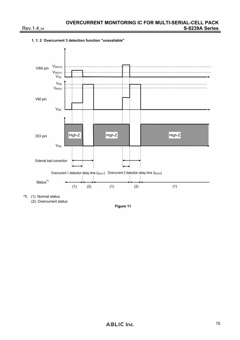
1. 1. 2 Overcurrent 3 detection function "unavailable"
(1) (2)(1)(2) (1)
VINI pin
DO pin
External load connection
Overcurrent 2 detection delay time (tDIOV2)
VM pin
Overcurrent 1 detection delay time (tDIOV1)
VSS
Status*1
VSS
VSS
VDIOV1
VDIOV2
High-Z High-Z High-Z
VDD VRIOV
*1. (1): Normal status (2): Overcurrent status
Figure 11

OVERCURRENT MONITORING IC FOR MULTI-SERIAL-CELL PACK S-8239A Series Rev.1.4_04
16
1. 2 Active "H"
1. 2. 1 Overcurrent 3 detection function "available"
(1)(2)(1)(2) (1)
VINI pin
DO pin
VM pin
VSS
Status*1
VSS
VSS
VDIOV1 VDIOV2
VDD VRIOV
VDIOV3
(2) (1)
External load connection
Overcurrent 1 detection delay time (tDIOV1) Overcurrent 2 detection delay time (tDIOV2) Overcurrent 3 detection delay time (tDIOV3)
High-Z High-Z High-Z
*1. (1): Normal status
(2): Overcurrent status Figure 12

OVERCURRENT MONITORING IC FOR MULTI-SERIAL-CELL PACKRev.1.4_04 S-8239A Series
17
1. 2. 2 Overcurrent 3 detection function "unavailable"
(1) (2)(1)(2) (1)
VINI pin
DO pin
VM pin
VSS
VSS
VSS
VDIOV1
VDIOV2
VDD VRIOV
External load connection
Status*1
Overcurrent 1 detection delay time (tDIOV1) Overcurrent 2 detection delay time (tDIOV2)
High-Z High-Z
*1. (1): Normal status
(2): Overcurrent status Figure 13
OVERCURRENT MONITORING IC FOR MULTI-SERIAL-CELL PACK S-8239A Series Rev.1.4_04
18
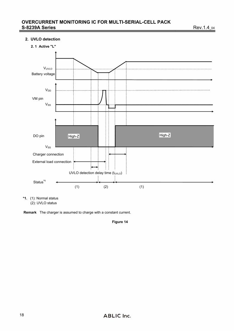
2. UVLO detection
2. 1 Active "L"
(1)
VSS
VSS
VUVLO
VDD
(2) (1)
High-Z High-Z DO pin
VM pin
Battery voltage
Status*1
External load connection
Charger connection
UVLO detection delay time (tUVLO)
*1. (1): Normal status (2): UVLO status
Remark The charger is assumed to charge with a constant current.
Figure 14
OVERCURRENT MONITORING IC FOR MULTI-SERIAL-CELL PACKRev.1.4_04 S-8239A Series
19
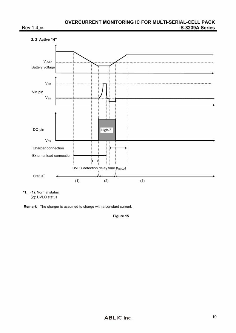
2. 2 Active "H"
(1)
VSS
VSS
VUVLO
VDD
(2) (1)
High-ZDO pin
VM pin
Battery voltage
Charger connection
External load connection
Status*1
UVLO detection delay time (tUVLO)
*1. (1): Normal status (2): UVLO status
Remark The charger is assumed to charge with a constant current.
Figure 15

OVERCURRENT MONITORING IC FOR MULTI-SERIAL-CELL PACK S-8239A Series Rev.1.4_04
20
5-serial-cell Protection Circuit Examples
Figure 16 and Figure 17 show the 5-serial-cell protection circuit examples used by the S-8239A Series and the S-8225A Series. Contact our sales office when using the circuit other than the following protection circuit examples. 1. Active "L"
DIS
CHA
EB
S-8225A Series*1
CTLD
CTLC
CO
DO
SEL1
SEL2
CDT
CCT
VDD
VC1
VC2
VC3
VC4
VC5
VC6
VSS
VM
DO
VINI
DP
VDD
VSS
S-8239A Series
1 M0.1 F
CVDD
CFET DFET
RDO
RDOPRVM330 k FET1*2
RSENSE
RVDD
FET2*2
100
1 k
FET4
ZVINI 0.1 F
0.1 F 0.1 F
0.1 F
0.1 F
0.1 F
0.1 F
0.1 F
0.1 F
1 M
1 M
FET3
RVINI
1 k
1 k
1 k
1 k
100
1 k
1 k
1 k
1 k
1 k
1 k
Figure 16
2. Active "H"
DIS
CHA
EB
S-8225A Series*1
CTLD
CTLC
CO
DO
SEL1
SEL2
CDT
CCT
VDD
VC1
VC2
VC3
VC4
VC5
VC6
VSS
VM
DO
VINI
DP
VDD
VSS
S-8239A Series
1 M0.1 F
CVDD
CFET DFET
RDO
RVM330 k FET1*2
RSENSE
RVDD
FET2*2
100
1 k
FET4
ZVINI 0.1 F
0.1 F 0.1 F
0.1 F
0.1 F
0.1 F
0.1 F
0.1 F
0.1 F
1 M
1 M
FET3
RVINI
FET5
RDOP 1 M
1 k
1 k
1 k
1 k
1 k
1 k
1 k
1 k
1 k
1 k
100
Figure 17
OVERCURRENT MONITORING IC FOR MULTI-SERIAL-CELL PACKRev.1.4_04 S-8239A Series
21
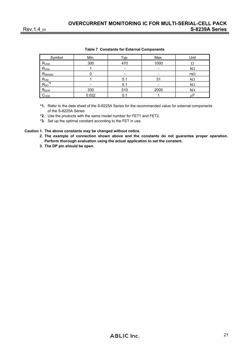
Table 7 Constants for External Components
Symbol Min. Typ. Max. Unit
RVDD 300 470 1000 RVINI 1 k
RSENSE 0 m
RVM 1 5.1 51 k
RDO*3 5.1 k
RDOP 330 510 2000 k
CVDD 0.022 0.1 1 F
*1. Refer to the data sheet of the S-8225A Series for the recommended value for external components
of the S-8225A Series. *2. Use the products with the same model number for FET1 and FET2. *3. Set up the optimal constant according to the FET in use.
Caution 1. The above constants may be changed without notice.
2. The example of connection shown above and the constants do not guarantee proper operation. Perform thorough evaluation using the actual application to set the constant.
3. The DP pin should be open.

OVERCURRENT MONITORING IC FOR MULTI-SERIAL-CELL PACK S-8239A Series Rev.1.4_04
22
Precautions The application conditions for the input voltage, output voltage, and load current should not exceed the package power
dissipation.
Do not apply an electrostatic discharge to this IC that exceeds the performance ratings of the built-in electrostatic protection circuit.
ABLIC Inc. claims no responsibility for any and all disputes arising out of or in connection with any infringement by products including this IC of patents owned by a third party.
OVERCURRENT MONITORING IC FOR MULTI-SERIAL-CELL PACKRev.1.4_04 S-8239A Series
23
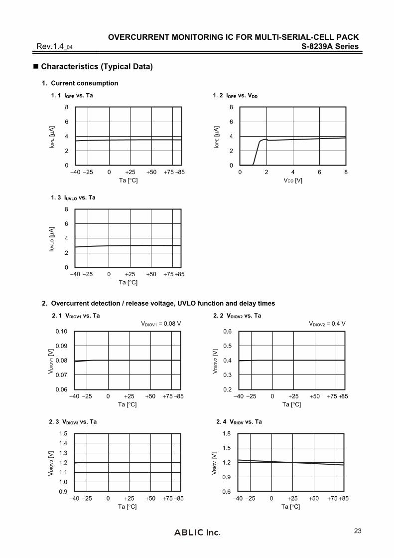
Characteristics (Typical Data) 1. Current consumption
1. 1 IOPE vs. Ta 1. 2 IOPE vs. VDD
IOP
E [μ
A]
0
8
−40 0 +25 +50 +75 + 85−25Ta [°C]
6
4
2
IOP
E [μ
A]
8VDD [V]
00
8
6
4
2
642
1. 3 IUVLO vs. Ta
IUV
LO [μ
A]
0
8
−40 0 +25 +50 +75 + 85−25Ta [°C]
6
4
2
2. Overcurrent detection / release voltage, UVLO function and delay times
2. 1 VDIOV1 vs. Ta VDIOV1 = 0.08 V
2. 2 VDIOV2 vs. Ta VDIOV2 = 0.4 V
VD
IOV
1 [V
]
0.06
0.10
−40 0 25 50 +75 + 85−25Ta [°C]
0.09
0.08
0.07 VD
IOV
2 [V
]
0.2
0.6
−40 0 25 50 +75 + 85−25Ta [°C]
0.5
0.4
0.3
2. 3 VDIOV3 vs. Ta 2. 4 VRIOV vs. Ta
VD
IOV
3 [V
]
−40 0 25 50 +75 + 85−25Ta [°C]
0.9
1.5
1.31.4
1.21.11.0
VR
IOV [V
]
0.6
1.8
−40 0 +25 +50 +75 +85−25Ta [°C]
1.5
1.2
0.9
OVERCURRENT MONITORING IC FOR MULTI-SERIAL-CELL PACK S-8239A Series Rev.1.4_04
24
2. 5 VDIOV1 vs. VDD
VDIOV1 = 0.08 V2. 6 VDIOV2 vs. VDD
VDIOV2 = 0.4 V
VD
IOV
1 [V
]
8VDD [V]
20.06
0.10
0.09
0.08
0.07
76543
VD
IOV
2 [V
]
8VDD [V]
20.2
0.6
0.5
0.4
0.3
76543
2. 7 VDIOV3 vs. VDD 2. 8 VRIOV vs. VDD
VD
IOV
3 [V
]
8VDD [V]
20.9
1.5
1.31.4
1.21.11.0
76543
VR
IOV [V
]
8VDD [V]
20.6
1.8
1.5
1.2
0.9
76543
2. 9 tDIOV1 vs. Ta
tDIOV1 = 1150 ms
2. 10 tDIOV2 vs. Ta
tDIOV2 = 1.12 ms
tDIO
V1 [
s]
0.8
1.6
−40 0 +25 +50 +75 +85−25Ta [°C]
1.4
1.2
1.0 tDIO
V2 [
ms]
0.8
1.6
−40 0 +25 +50 +75 +85−25Ta [°C]
1.4
1.2
1.0
2. 11 tDIOV3 vs. Ta
2. 12 tDIOV1 vs. VDD
tDIOV1 = 1150 ms
tDIO
V3 [
μs]
160
400
−40 0 +25 +50 +75 +85−25Ta [°C]
340
280
220
tDIO
V1 [
s]
8VDD [V]
20.8
1.6
1.4
1.2
1.0
76543
OVERCURRENT MONITORING IC FOR MULTI-SERIAL-CELL PACKRev.1.4_04 S-8239A Series
25
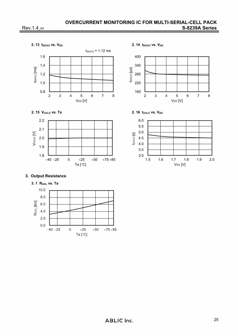
2. 13 tDIOV2 vs. VDD
tDIOV2 = 1.12 ms
2. 14 tDIOV3 vs. VDD
tDIO
V2 [
ms]
8VDD [V]
20.8
1.6
1.4
1.2
1.0
76543
tDIO
V3 [
μs]
8VDD [V]
2160
400
340
280
220
76543
2. 15 VUVLO vs. Ta 2. 16 tUVLO vs. VDD
VU
VLO
[V]
1.8
2.2
−40 0 25 50 +75 +85−25Ta [°C]
2.1
2.0
1.9
tUV
LO [s
]
2.0VDD [V]
1.53.0
6.0
1.91.81.71.6
5.55.04.54.03.5
3. Output Resistance
3. 1 RDOL vs. Ta
RD
OL [
k]
0.0
8.0
40 0 25 50 75 8525Ta [C]
6.0
4.0
2.0
10.0

OVERCURRENT MONITORING IC FOR MULTI-SERIAL-CELL PACK S-8239A Series Rev.1.4_04
26
Marking Specification
1. SOT-23-6
1 2 3
46 5
Top view
(1) (2) (3) (4)
(1) to (3): Product code (Refer to Product name vs. Product code) (4): Lot number
Product name vs. Product code
Product Name Product Code
(1) (2) (3)
S-8239AAA-M6T1U 3 S A
S-8239AAB-M6T1U 3 S B
S-8239AAC-M6T1U 3 S C
S-8239AAD-M6T1U 3 S D
S-8239AAE-M6T1U 3 S E
S-8239AAF-M6T1U 3 S F
S-8239AAG-M6T1U 3 S G
S-8239AAH-M6T1U 3 S H
S-8239AAI-M6T1U 3 S I
S-8239AAJ-M6T1U 3 S J
S-8239AAK-M6T1U 3 S K
���
�����
���
����
������ ��
�� ����
����
�� ����
� � �
�� �
���������
�� �
�����������
�� �
��
�������������������
���������������
��������������� !"��!"

���
�����
���
����
������ ��
��
���
� � �
#���������
��������
#��������� �������
�������
��������
�������
�����������$�������
�������$�������
��������$%&& � & � �%'
( )�)�& *+��!
�������,���'�+*- ".��������/

���
�����
���
����
������ ��
��
�����%0�
������
#������
,��1/ ,��1/
2�3 �4���
�!5%&6 )�)&%7�!6��!�+- �* !+&%5�'%&+
�����������8�������
�������8�������
��������8 5
Disclaimers (Handling Precautions)
1. All the information described herein (product data, specifications, figures, tables, programs, algorithms and application circuit examples, etc.) is current as of publishing date of this document and is subject to change without notice.
2. The circuit examples and the usages described herein are for reference only, and do not guarantee the success of any specific mass-production design. ABLIC Inc. is not responsible for damages caused by the reasons other than the products described herein (hereinafter "the products") or infringement of third-party intellectual property right and any other right due to the use of the information described herein.
3. ABLIC Inc. is not responsible for damages caused by the incorrect information described herein.
4. Be careful to use the products within their specified ranges. Pay special attention to the absolute maximum ratings, operation voltage range and electrical characteristics, etc. ABLIC Inc. is not responsible for damages caused by failures and / or accidents, etc. that occur due to the use of the products outside their specified ranges.
5. When using the products, confirm their applications, and the laws and regulations of the region or country where they are used and verify suitability, safety and other factors for the intended use.
6. When exporting the products, comply with the Foreign Exchange and Foreign Trade Act and all other export-related laws, and follow the required procedures.
7. The products must not be used or provided (exported) for the purposes of the development of weapons of mass destruction or military use. ABLIC Inc. is not responsible for any provision (export) to those whose purpose is to develop, manufacture, use or store nuclear, biological or chemical weapons, missiles, or other military use.
8. The products are not designed to be used as part of any device or equipment that may affect the human body, human life, or assets (such as medical equipment, disaster prevention systems, security systems, combustion control systems, infrastructure control systems, vehicle equipment, traffic systems, in-vehicle equipment, aviation equipment, aerospace equipment, and nuclear-related equipment), excluding when specified for in-vehicle use or other uses. Do not apply the products to the above listed devices and equipments without prior written permission by ABLIC Inc. Especially, the products cannot be used for life support devices, devices implanted in the human body and devices that directly affect human life, etc. Prior consultation with our sales office is required when considering the above uses. ABLIC Inc. is not responsible for damages caused by unauthorized or unspecified use of our products.
9. Semiconductor products may fail or malfunction with some probability. The user of the products should therefore take responsibility to give thorough consideration to safety design including redundancy, fire spread prevention measures, and malfunction prevention to prevent accidents causing injury or death, fires and social damage, etc. that may ensue from the products' failure or malfunction. The entire system must be sufficiently evaluated and applied on customer's own responsibility.
10. The products are not designed to be radiation-proof. The necessary radiation measures should be taken in the product design by the customer depending on the intended use.
11. The products do not affect human health under normal use. However, they contain chemical substances and heavy metals and should therefore not be put in the mouth. The fracture surfaces of wafers and chips may be sharp. Be careful when handling these with the bare hands to prevent injuries, etc.
12. When disposing of the products, comply with the laws and ordinances of the country or region where they are used.
13. The information described herein contains copyright information and know-how of ABLIC Inc. The information described herein does not convey any license under any intellectual property rights or any other rights belonging to ABLIC Inc. or a third party. Reproduction or copying of the information from this document or any part of this document described herein for the purpose of disclosing it to a third-party without the express permission of ABLIC Inc. is strictly prohibited.
14. For more details on the information described herein, contact our sales office.
2.0-2018.01
www.ablicinc.com