S-72.244 Modulation and Coding Methods · 2 Helsinki University of Technology, Communications...
25
1 S-72.244 Modulation and Coding Methods Linear Carrier Wave Modulation
-
Upload
phungtuyen -
Category
Documents
-
view
216 -
download
0
Transcript of S-72.244 Modulation and Coding Methods · 2 Helsinki University of Technology, Communications...
1
S-72.244 Modulation and Coding Methods
Linear Carrier Wave Modulation
2
Helsinki University of Technology, Communications Laboratory, Timo O. Korhonen
Linear carrier wave (CW) modulation
n Bandpass systems and signalsn Lowpass (LP) equivalentsn Amplitude modulation (AM)n Double-sideband modulation (DSB)n Modulator techniquesn Suppressed-sideband amplitude
modulation (LSB, USB)n Detection techniques of linear modulation
– Coherent detection– Noncoherent detection
AM
DSB
LSB
USB
3
Helsinki University of Technology, Communications Laboratory, Timo O. Korhonen
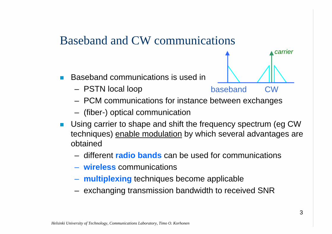
Baseband and CW communications
n Baseband communications is used in– PSTN local loop– PCM communications for instance between exchanges– (fiber-) optical communication
n Using carrier to shape and shift the frequency spectrum (eg CW techniques) enable modulation by which several advantages are obtained– different radio bands can be used for communications– wireless communications– multiplexing techniques become applicable– exchanging transmission bandwidth to received SNR
CWbaseband
carrier

4
Helsinki University of Technology, Communications Laboratory, Timo O. Korhonen
Defining bandpass signals
n The bandpass signal is band limited
n We assume also that (why?)
n In telecommunications bandpass signals are used to convey messages over medium
n In practice, transmitted messages are never strictly band limited due to– their nature in frequency domain (Fourier series coefficients
may extend over very large span of frequencies)– non-ideal filtering
( ) 0,
( ) 0,otherwise
= < − ∧ > +
≠bp c c
bp
V f f f W f f W
V f
W fC
<<

5
Helsinki University of Technology, Communications Laboratory, Timo O. Korhonen
Example of a bandpass systemn Consider a simple bandpass system: a resonant (tank) circuit
zj L j C
j L j Cp=
+ω ω
ω ω/
/1z R zi p= + V H V
in out( ) ( ) ( )ω ω ω=
( ) ( ) / ( ) /out in p iH V V z zω ω ω= = 0 0( ) 1/[1 ( / / )]H jQ f f f fω⇒ = + +
10
/
(2 )
Q R C L
f LCπ −
=
=
pzTank circuit
6
Helsinki University of Technology, Communications Laboratory, Timo O. Korhonen
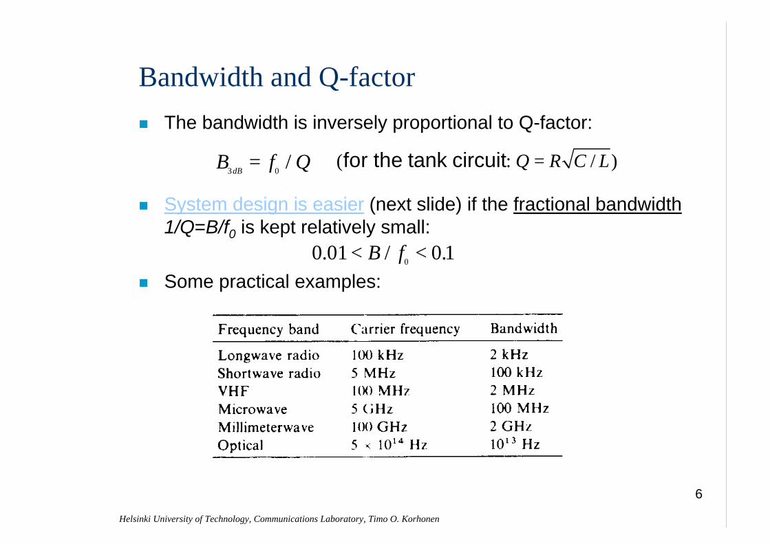
n The bandwidth is inversely proportional to Q-factor:
n System design is easier (next slide) if the fractional bandwidth1/Q=B/f0 is kept relatively small:
n Some practical examples:
Bandwidth and Q-factor
B f QdB3 0
= /
0 01 0 10
. / .< <B f
( : / )Q R C L=for the tank circuit

7
Helsinki University of Technology, Communications Laboratory, Timo O. Korhonen
Why system design is easier for smaller fractional bandwidths (FB)?
n Antenna and bandpass amplifier design is difficult for large FB:s:– one will have “difficult to realize” components or
parameters in circuits as • too high Q• too small or large values for capacitors and inductors
n These structures have a bandpass nature because one of their important elements is the resonant circuit. Making them broadband means decreasing resistive losses that can be difficult
8
Helsinki University of Technology, Communications Laboratory, Timo O. Korhonen
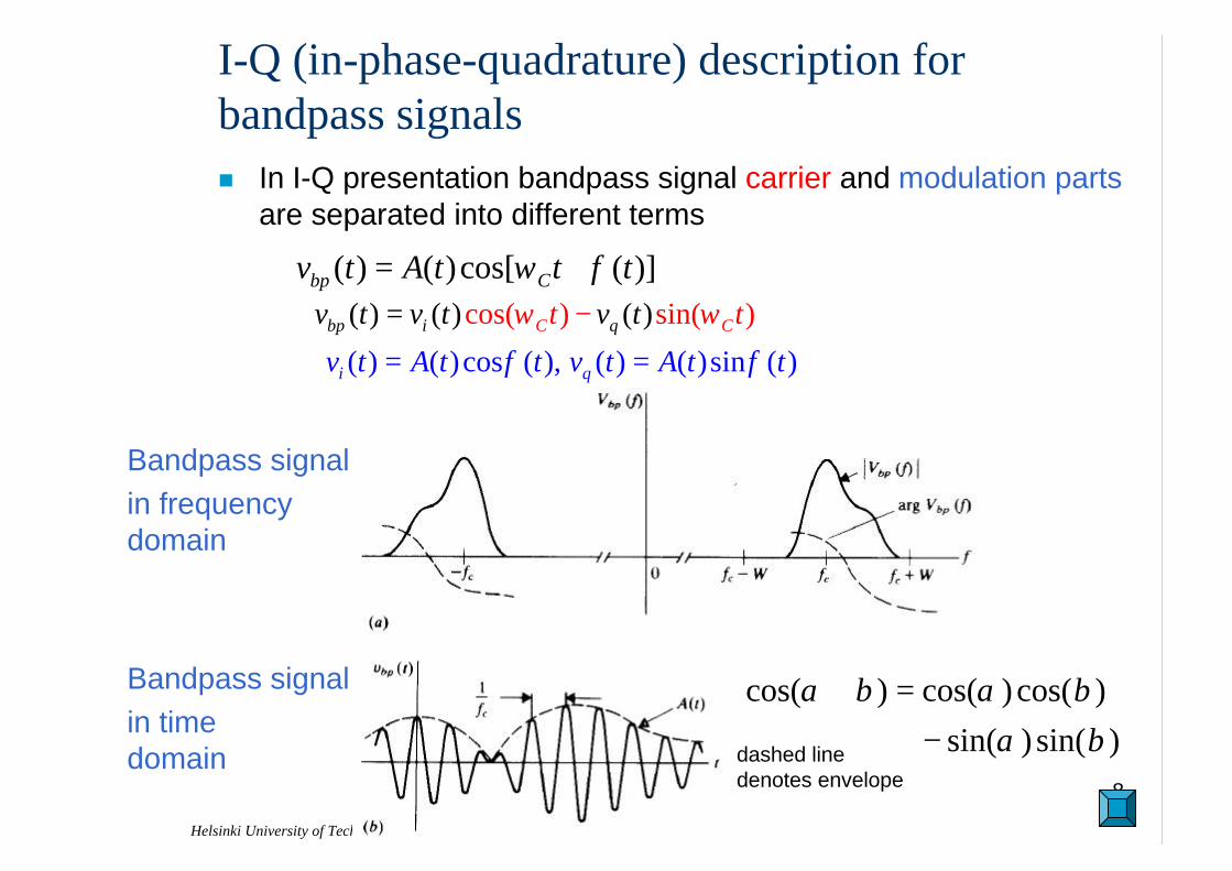
I-Q (in-phase-quadrature) description for bandpass signalsn In I-Q presentation bandpass signal carrier and modulation parts
are separated into different terms
( ) ( )cos[ ( )]bp Cv t A t t tω φ= +( ) ( ) ( )cos( ) sin( )Cbp i q Cv t v tt tt vω ω= −
( ) ( )cos ( ), ( ) ( )sin ( )i qv t A t t v t A t tφ φ= =
cos( ) cos( )cos( )sin( ) sin( )
α β α βα β
+ =−
Bandpass signalin frequencydomain
Bandpass signalin timedomain dashed line
denotes envelope
9
Helsinki University of Technology, Communications Laboratory, Timo O. Korhonen
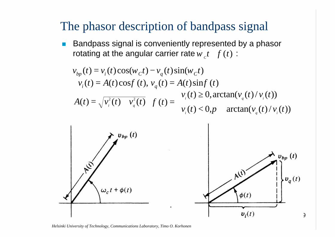
The phasor description of bandpass signaln Bandpass signal is conveniently represented by a phasor
rotating at the angular carrier rate :
A t v t v ti q( ) ( ) ( )= +2 2
( ) ( )cos( ) ( )sin( )bp i C q Cv t v t t v t tω ω= −( ) ( )cos ( ), ( ) ( )sin ( )i qv t A t t v t A t tφ φ= =
( ) 0,arctan( ( ) / ( ))( )
( ) 0, arctan( ( ) / ( ))i q i
i q i
v t v t v tt
v t v t v tφ
π
≥= < +
ω φCt t+ ( )
10
Helsinki University of Technology, Communications Laboratory, Timo O. Korhonen
Lowpass (LP) signal
n Lowpass signal is defined byyielding in time domain
Taking rectangular-polar conversion yields then
12( ) ( ) ( )lp i qV f V f jV f + @
( ) ( )cos( ) ( )sin( )
( ) ( )cos ( )
( ) ( )sin ( )
bp i c q c
i
q
v t v t t v t t
v t A t t
v t A t t
ω ω
φφ
= + = =
1 12( ) ( ) ( ) ( )lp lp i qv t V f v t jv t− = = + F
[ ]( ) ( ) cos ( ) sin ( ) / 2
( ) ( ) / 2, arg ( ) ( )
lp
lp lp
v t A t t j t
v t A t v t t
φ φ
φ
= +
= =
⇒ 12( ) ( )exp ( )lpv t A t j tφ=

11
Helsinki University of Technology, Communications Laboratory, Timo O. Korhonen
Transforming lowpass signals and bandpass signals
n Physically this means that the lowpass signal is modulated to the carrier frequency ω when it is transformed to bandpass signal. Bandpass signal can be transformed into lowpass signal by (tutorials). What is the physical meaning of this?
{ }Re ( )exp[ ( )]bp cv A t j t tω φ= +
( ) ( )cos[ ( )]bp cv t A t t tω φ= +
( )
( )2Re exp[ ( )]exp[ ]
2lp
bp c
v t
A tv j t j tφ ω
= 1442443
{ }2Re ( )exp[ ]bp lp cv v t j tω=
( ) ( ) ( )lp bp C CV f V f uf f f+= +

12
Helsinki University of Technology, Communications Laboratory, Timo O. Korhonen
Amplitude modulation (AM)n We discuss three linear mod. methods: (1) AM (amplitude
modulation), (2) DSB (double sideband modulation), (3) SSB (single sideband modulation)
n AM signal:
n φ(t) is an arbitrary constant. Hence we note that no information is transmitted via the phase. Assume for instance that φ(t)=0, then the LP components are
n Also, the carrier component contains no information-> Waste of power to transmit the unmodulated carrier, but can still be useful (how?)
Carrier Information carrying part
( ) [1 ( )]cos( ( ))
cos( ( )) ( )cos( ( ))C c m c
c c c m c
x t A x t t t
A t t A x t t t
µ ω φω φ µ ω φ
= + += + + +1442443 144424443
( ) ( )cos( ( )) ( ) [1 ( )]
( ) ( )sin( ( )) 0i c m
q
v t A t t A t A x t
v t A t t
φ µφ
= = = += =
0 1
( ) 1mx t
µ≤ ≤ ≤
13
Helsinki University of Technology, Communications Laboratory, Timo O. Korhonen
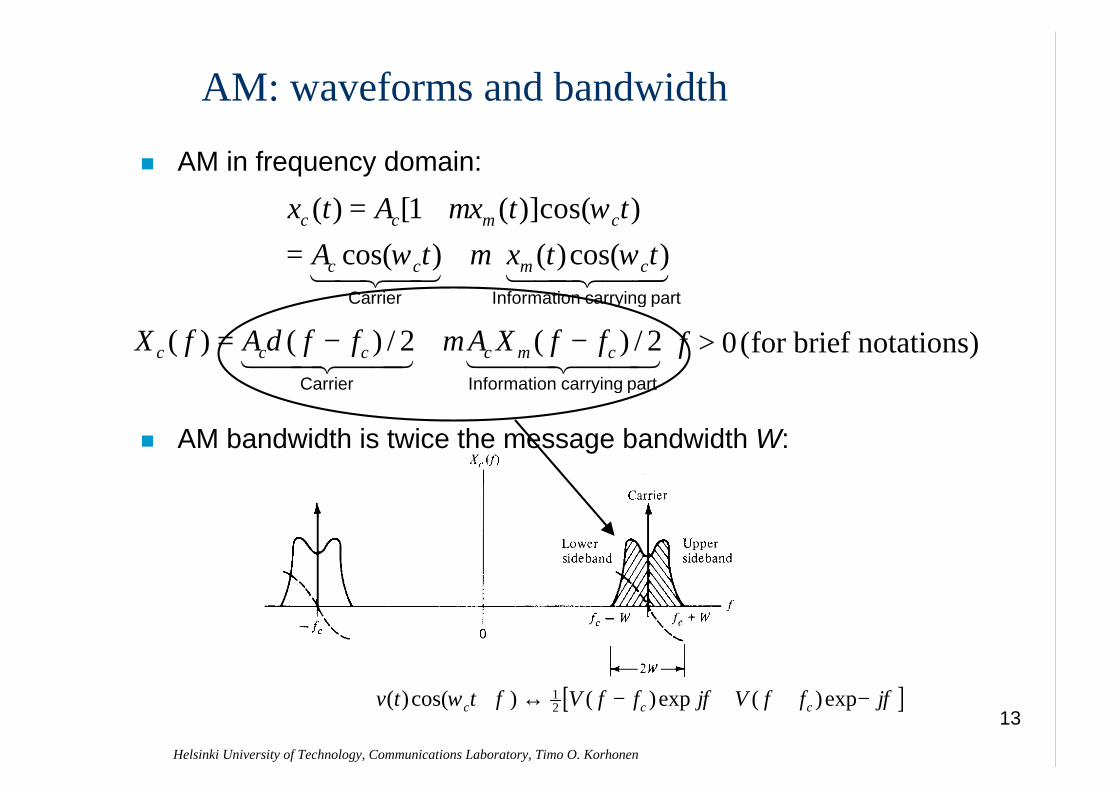
AM: waveforms and bandwidth
n AM in frequency domain:
n AM bandwidth is twice the message bandwidth W:
( ) [1 ( )]cos( )
cos( ) ( )cos( )c c m c
c c m c
x t A x t t
A t x t t
µ ωω µ ω
= += +14243 1442443
Carrier Information carrying part
( ) ( ) / 2 ( ) / 2c c c c m cX f A f f A X f fδ µ= − + −1442443 1442443Carrier Information carrying part
f > 0( )for brief notations
[ ]12( )cos( ) ( )exp ( )expc c cv t t V f f j V f f jω φ φ φ+ ↔ − + + −
14
Helsinki University of Technology, Communications Laboratory, Timo O. Korhonen
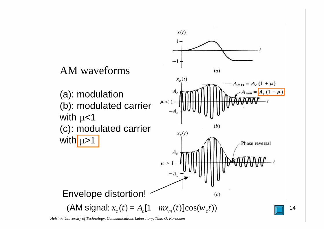
AM waveforms
(a): modulation(b): modulated carrierwith µ<1(c): modulated carrierwith µ>1
Envelope distortion!( : ( ) [1 ( )]cos( ))c c m cx t A x t tµ ω= +AM signal

15
Helsinki University of Technology, Communications Laboratory, Timo O. Korhonen
AM power efficiencyn AM wave total power consists of the idle carrier part and the
useful signal part:
n Assume AC=1, SX=1, then for µ=1 (the max value) the total power is
n Therefore at least half of the total power is wasted on carriern Detection of AM is simple by enveloped detector that is a reason
why AM is still used. Also, sometimes AM makessystem design easier, as in fiber opticcommunications
{
{X
2 2 2
Carrier
2 2 2 2
Power: S
2 2 2
2
( ) cos ( )
( ) cos ( )
/ 2 / 2C SB
c c c
c m c
c c X
P P
x t A t
A x t t
A A S
ω
µ ω
µ
< >= < >
+ < >
= +
1442443
14243
PT max / /= +1 2 1 2Carrier power Modulation power3 3
( : ( )
[1 ( )]cos( ))c
c m c
x t
A x t tµ ω=
+AM signal

16
Helsinki University of Technology, Communications Laboratory, Timo O. Korhonen
n In DSB the wasteful carrier is suppressed:
n The spectra is otherwise identical to AM and the transmission BW equals again double the message BW
n In time domain each modulation signal zero crossing produces phase reversals of the carrier. For DSB, the total power ST and the power/sideband PSB have the relationship
n Therefore AM transmitter requires twice the power of DSB transmitter to produce the same coverage assuming SX=1. However, in practice SX is usually smaller than 1/2, under which condition at least four times the DSB power is required for the AM transmitter for the same coverage
DSB signals and spectra
( ) ( )cos( )c c m cx t A x t tω=
( ) ( ) / 2, 0c c m cX f A X f f f= − >
2 / 2 2T c X SB
S A S P= = ⇒ 2 / 4 ( )SB c XP A S DSB=
AM: ( ) [1 ( )]cos( )c c m c
x t A x t tµ ω= +
17
Helsinki University of Technology, Communications Laboratory, Timo O. Korhonen
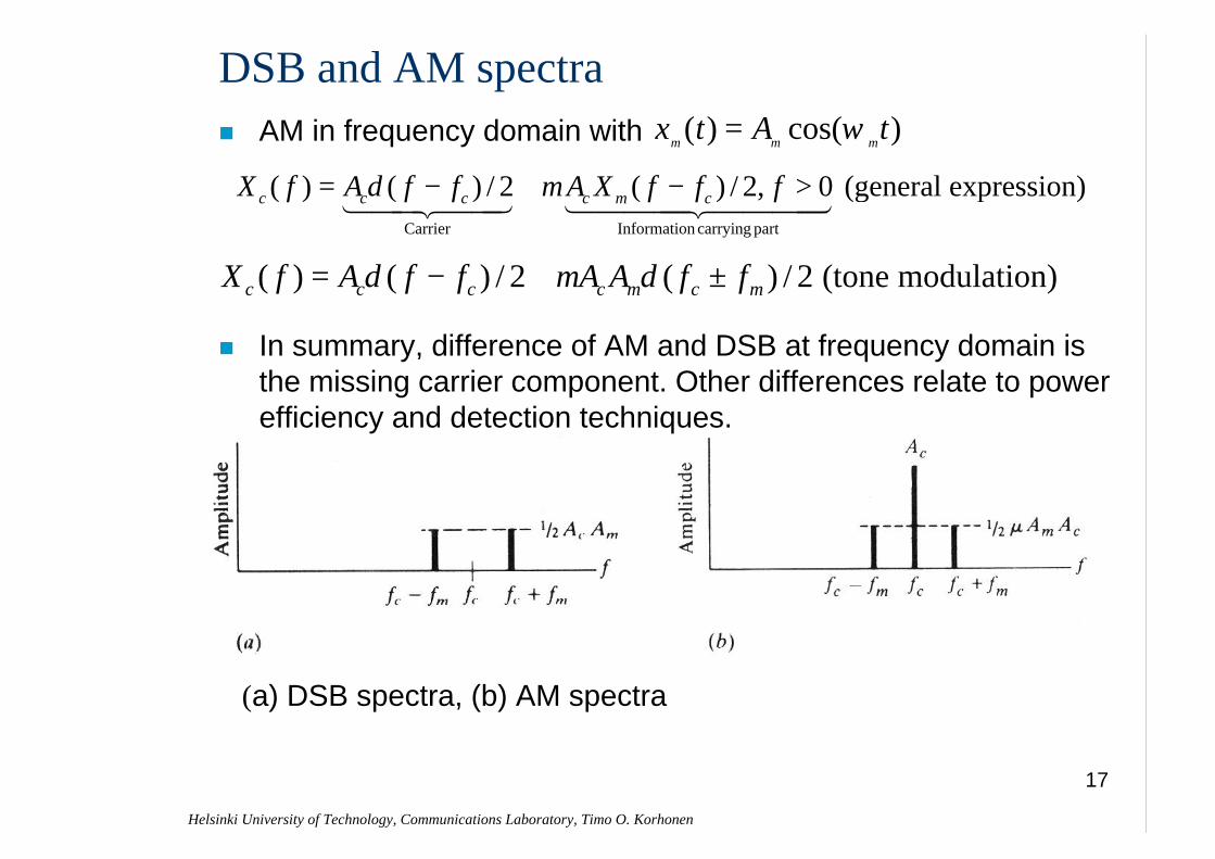
DSB and AM spectran AM in frequency domain with
n In summary, difference of AM and DSB at frequency domain is the missing carrier component. Other differences relate to powerefficiency and detection techniques.
x t A tm m m( ) cos( )= ω
Carrier Information carrying part
( ) ( ) / 2 ( ) / 2, 0 (general expression)c c c c m cX f A f f A X f f fδ µ= − + − >1442443 14444244443
( ) ( ) / 2 ( ) / 2 (tone modulation)c c c c m c mX f A f f A A f fδ µ δ= − + ±
(a) DSB spectra, (b) AM spectra
18
Helsinki University of Technology, Communications Laboratory, Timo O. Korhonen
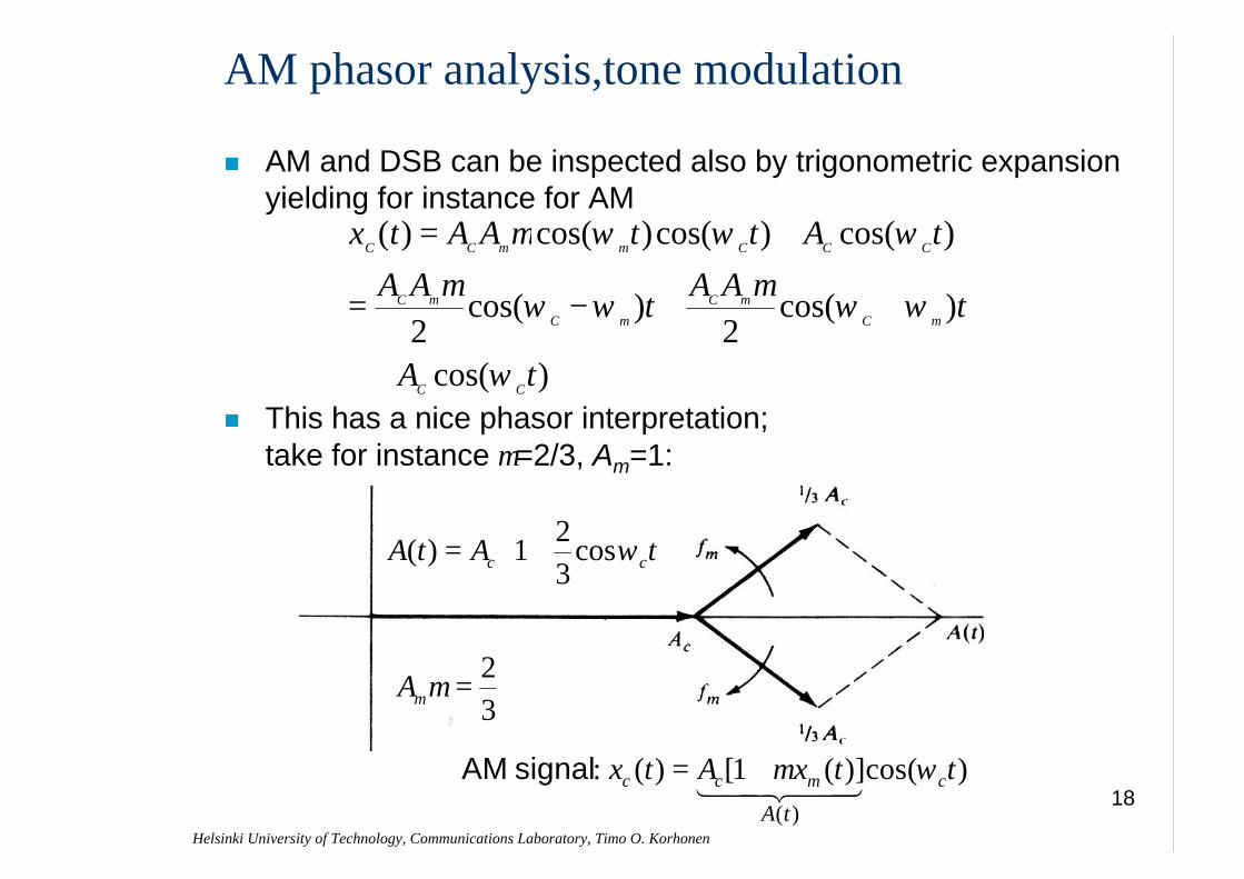
AM phasor analysis,tone modulation
n AM and DSB can be inspected also by trigonometric expansion yielding for instance for AM
n This has a nice phasor interpretation; take for instance µ=2/3, Am=1:
x t A A t t A t
A At
A At
A t
C C m m C C C
C m
C m
C m
C m
C C
( ) cos( )cos( ) cos( )
cos( ) cos( )
cos( )
= +
= − + +
+
µ ω ω ω
µω ω
µω ω
ω2 2
( )
: ( ) [1 ( )]cos( )c c m c
A t
x t A x t tµ ω= +1442443AM signal
23mA µ =
2( ) 1 cos
3c cA t A tω = +
19
Helsinki University of Technology, Communications Laboratory, Timo O. Korhonen
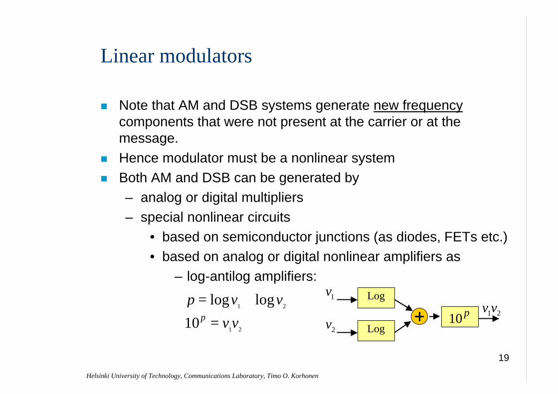
Linear modulators
n Note that AM and DSB systems generate new frequencycomponents that were not present at the carrier or at the message.
n Hence modulator must be a nonlinear systemn Both AM and DSB can be generated by
– analog or digital multipliers– special nonlinear circuits
• based on semiconductor junctions (as diodes, FETs etc.)• based on analog or digital nonlinear amplifiers as
– log-antilog amplifiers:
p v v
v vp
= +
=
log log1 2
1 210
Log
Log10 p
1v
2v1 2v v
20
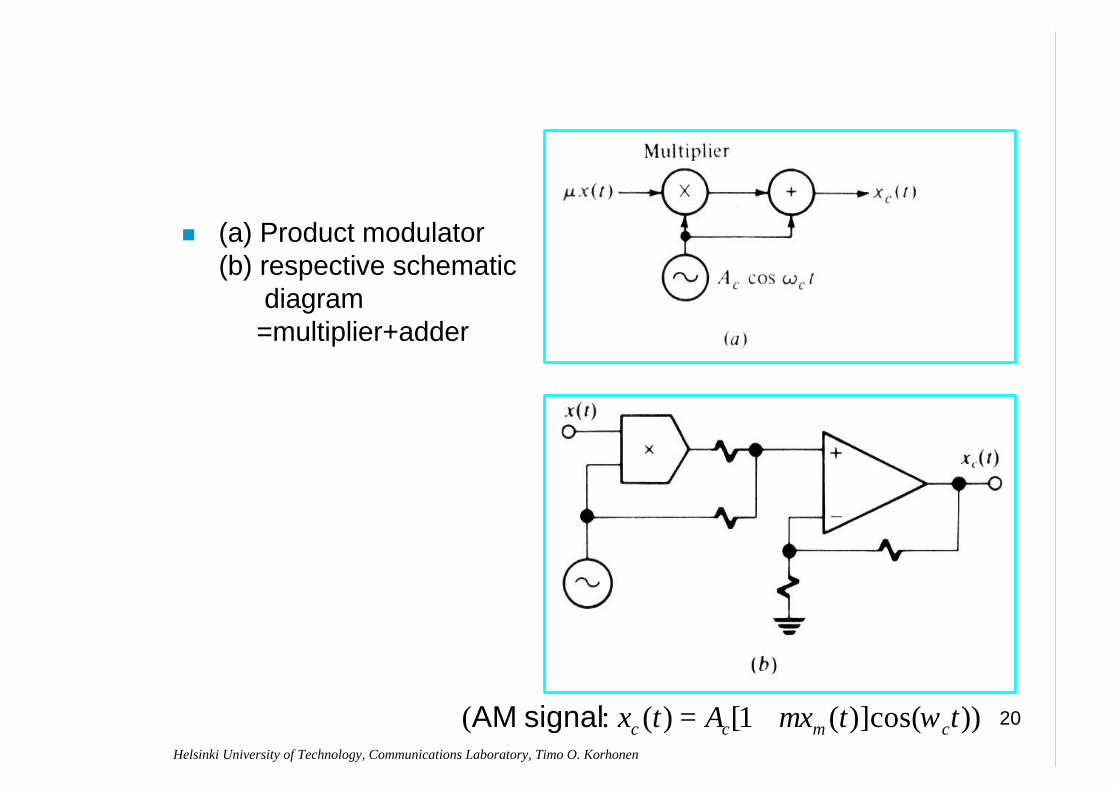
Helsinki University of Technology, Communications Laboratory, Timo O. Korhonen
n (a) Product modulator(b) respective schematic
diagram =multiplier+adder
( : ( ) [1 ( )]cos( ))c c m cx t A x t tµ ω= +AM signal
21
Helsinki University of Technology, Communications Laboratory, Timo O. Korhonen
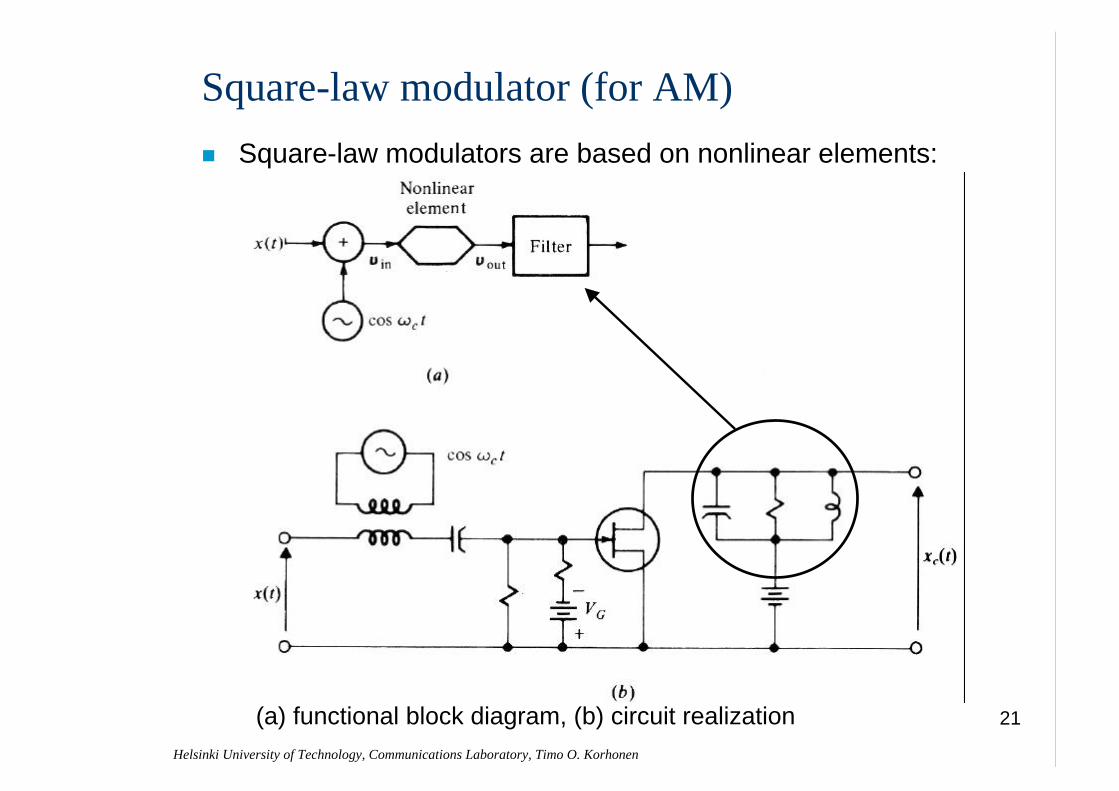
Square-law modulator (for AM)n Square-law modulators are based on nonlinear elements:
(a) functional block diagram, (b) circuit realization
22
Helsinki University of Technology, Communications Laboratory, Timo O. Korhonen
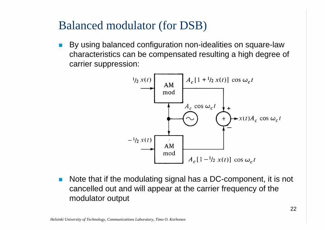
Balanced modulator (for DSB)n By using balanced configuration non-idealities on square-law
characteristics can be compensated resulting a high degree of carrier suppression:
n Note that if the modulating signal has a DC-component, it is not cancelled out and will appear at the carrier frequency of the modulator output
23
Helsinki University of Technology, Communications Laboratory, Timo O. Korhonen
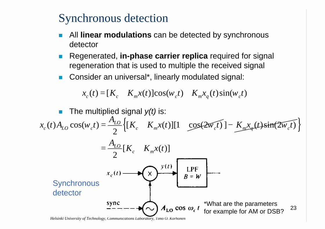
Synchronous detectionn All linear modulations can be detected by synchronous
detectorn Regenerated, in-phase carrier replica required for signal
regeneration that is used to multiple the received signaln Consider an universal*, linearly modulated signal:
n The multiplied signal y(t) is:
( ) [ ( )]cos( ) ( )sin( )c c c q cx t K K x t t K x t tµ µω ω= + +
( ) cos( ) [ ( )][1 cos(2 )2LO
c LO c c cA
x t A t K K x t tµω ω= + + ] ( )sin(2 )q cK x t tµ ω−{ }[ ( )]
2LO
cA
K K x tµ= +
Synchronousdetector
*What are the parametersfor example for AM or DSB?
24
Helsinki University of Technology, Communications Laboratory, Timo O. Korhonen
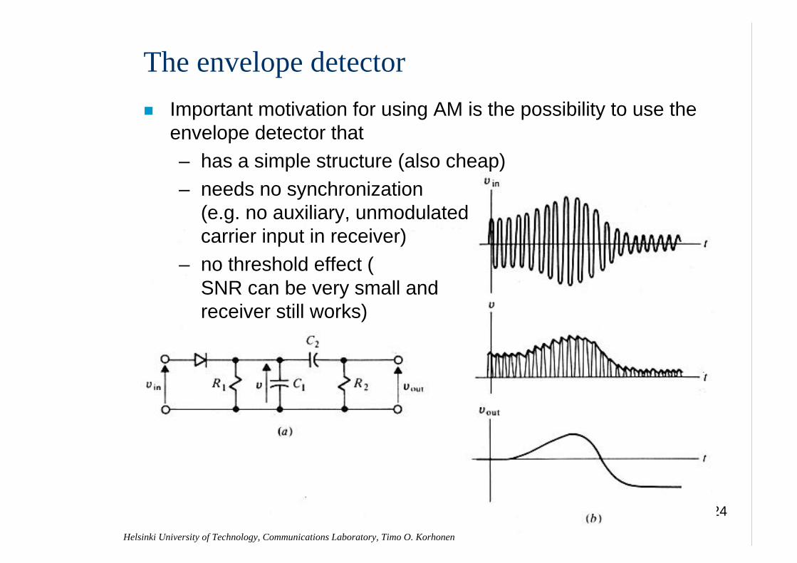
The envelope detectorn Important motivation for using AM is the possibility to use the
envelope detector that – has a simple structure (also cheap) – needs no synchronization
(e.g. no auxiliary, unmodulated carrier input in receiver)
– no threshold effect (SNR can be very small and receiver still works)
25
Helsinki University of Technology, Communications Laboratory, Timo O. Korhonen
Envelope detector analyzed
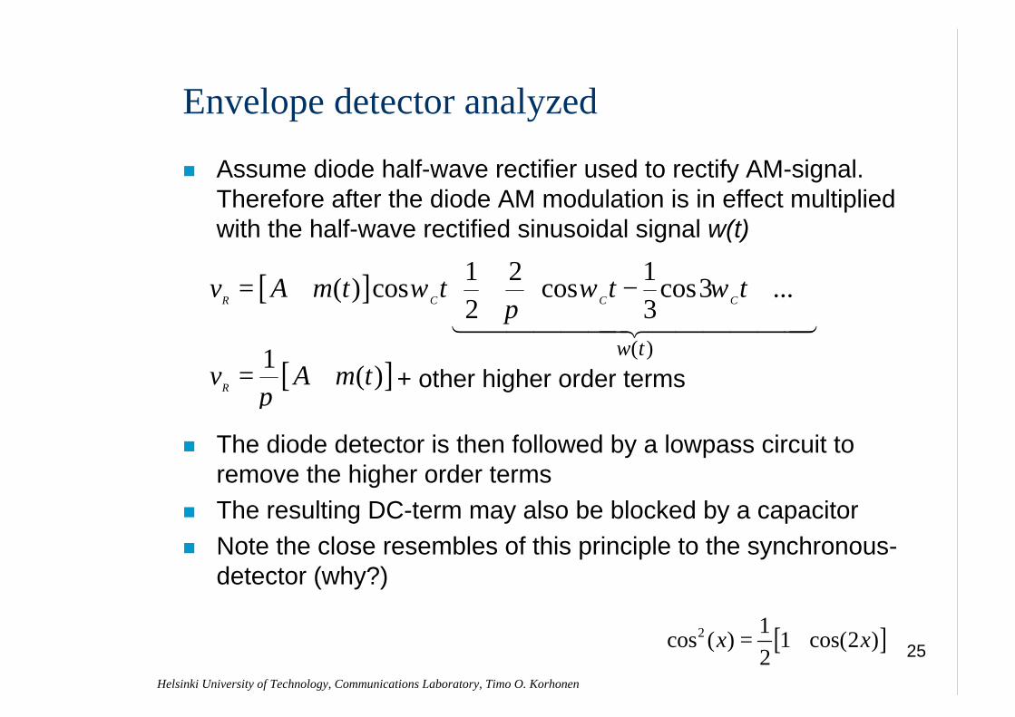
n Assume diode half-wave rectifier used to rectify AM-signal. Therefore after the diode AM modulation is in effect multiplied with the half-wave rectified sinusoidal signal w(t)
n The diode detector is then followed by a lowpass circuit to remove the higher order terms
n The resulting DC-term may also be blocked by a capacitorn Note the close resembles of this principle to the synchronous-
detector (why?)
[ ]
( )
1 2 1( ) cos cos cos3 ...
2 3R C C C
w t
v A m t t t tω ω ωπ
= + + − + 144444424444443[ ]1
( )Rv A m tπ
= + + other higher order terms
[ ]2 1cos ( ) 1 cos(2 )
2x x= +