S-100 COMPUTER LIGHT PEN PROJECT.
13
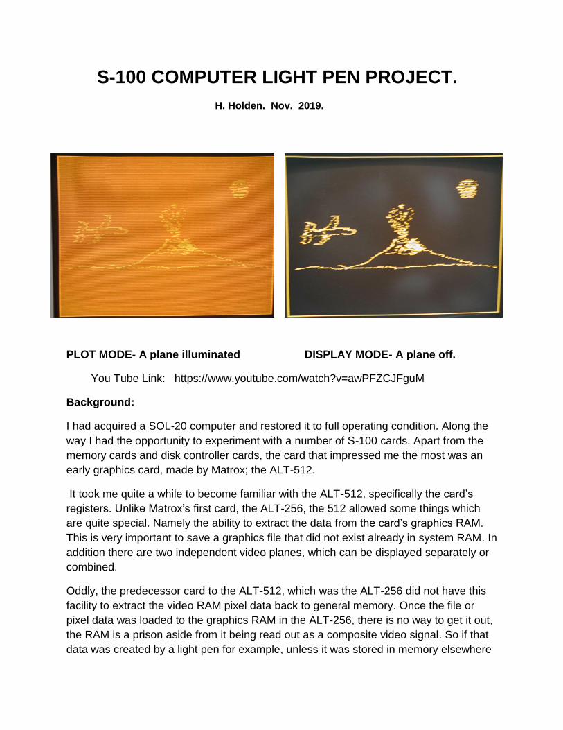
S-100 COMPUTER LIGHT PEN PROJECT. H. Holden. Nov. 2019. PLOT MODE- A plane illuminated DISPLAY MODE- A plane off. You Tube Link: https://www.youtube.com/watch?v=awPFZCJFguM Background: I had acquired a SOL-20 computer and restored it to full operating condition. Along the way I had the opportunity to experiment with a number of S-100 cards. Apart from the memory cards and disk controller cards, the card that impressed me the most was an early graphics card, made by Matrox; the ALT-512. It took me quite a while to become familiar with the ALT-512, specifically the card’s registers. Unlike Matrox’s first card, the ALT-256, the 512 allowed some things which are quite special. Namely the ability to extract the data from the card’s graphics RAM. This is very important to save a graphics file that did not exist already in system RAM. In addition there are two independent video planes, which can be displayed separately or combined. Oddly, the predecessor card to the ALT-512, which was the ALT-256 did not have this facility to extract the video RAM pixel data back to general memory. Once the file or pixel data was loaded to the graphics RAM in the ALT-256, there is no way to get it out, the RAM is a prison aside from it being read out as a composite video signal. So if that data was created by a light pen for example, unless it was stored in memory elsewhere
Transcript of S-100 COMPUTER LIGHT PEN PROJECT.
S-100 COMPUTER LIGHT PEN PROJECT.
H. Holden. Nov. 2019.
PLOT MODE- A plane illuminated DISPLAY MODE- A plane off.
You Tube Link: https://www.youtube.com/watch?v=awPFZCJFguM
Background:
I had acquired a SOL-20 computer and restored it to full operating condition. Along the
way I had the opportunity to experiment with a number of S-100 cards. Apart from the
memory cards and disk controller cards, the card that impressed me the most was an
early graphics card, made by Matrox; the ALT-512.
It took me quite a while to become familiar with the ALT-512, specifically the card’s
registers. Unlike Matrox’s first card, the ALT-256, the 512 allowed some things which
are quite special. Namely the ability to extract the data from the card’s graphics RAM.
This is very important to save a graphics file that did not exist already in system RAM. In
addition there are two independent video planes, which can be displayed separately or
combined.
Oddly, the predecessor card to the ALT-512, which was the ALT-256 did not have this
facility to extract the video RAM pixel data back to general memory. Once the file or
pixel data was loaded to the graphics RAM in the ALT-256, there is no way to get it out,
the RAM is a prison aside from it being read out as a composite video signal. So if that
data was created by a light pen for example, unless it was stored in memory elsewhere

(which is time consuming in the software program), around the same time it was
generated and sent to the graphics RAM, it was not retrievable. So the ALT-512
provided distinct advantages for a light pen project, especially for a high speed light pen
system.
The first steps required the ability to write from a disk file to general memory in the SOL-
20. Then from general memory to the ALT-512’s graphics RAM. Then to extract that file
from the graphics ram to memory and then be able to save that file to a named disk file.
So I had to master the 8080 assembly language programs to do that, before I started on
the light pen Project, or I would not be able to store and re-display any light pen art work
that I created.
There are a number of ways a light pen could be implemented, either largely in software
or in hardware. I decided to go down the about 80% hardware 20% software route in the
interests of speed and performance.
Design Concept:
The light pen, which is basically a photo transistor needs to “see” some light to initially
generate a signal. Various tricks have been used to get this to work, such as strobing
raster locations with bright rectangles or just increasing the CRT’s brightness. Most
commercial light pens have a phototransistor and a cmos hex inverter IC in them and
sometimes one or two transistors. The pen itself is not complex. A number of pens were
made for Commodore computers which plug onto their game’s port and use the support
electronics and software there. I elected to use a dual button pen which focuses on a
pixel without the pen needing to touch the faceplate of the CRT:

I decided that since the ALT-512 can produce two simultaneously displayed graphics
planes (256 x 240 pixels) I could have one plane as the “illumination plane” and the
other as the plane to write to. Then, after the image was plotted, I could simply turn off
the illumination plane. This way I would not have to scan the CRT’s face with
progressive illuminated pixels, slowing the proceedings, or have to alter the video
monitor’s brightness or contrast controls to get the pen working.
I could not find any schematics of light pen processing circuits at all, except a basic
block diagram showing that the idea consisted of a horizontal counter, to keep track of
the pixel count along one scanning line(X counter) and a line counter to keep track of
these scanning lines(Y counter) and these track the pixel counters on the graphics card
it was said. The idea being that when the light pen sees a signal, those counters are
stopped. Then, the X and Y counts are used to provide address coordinates for the pixel
to be illuminated.
Technical Challenges:
While the principles of operation seemed simple enough, there where some interesting
challenges. Firstly the actual video data which reaches the video monitor is not exactly
time synchronized with the counters in the graphic’s card. This is because the video
graphics card’s RAM data is clocked out of the graphics card by a shift register and
there is a 12 pixel clock delay before it exits the card to create the composite video
signal.
Rather than pre-loading the X coordinate counters on my circuit card with initial values
to get around this (could have been one option) I decided to create a digital delay with a
separate counter (74LS93 & gates) instead.
In addition, as well as stopping the counters, their resets must also be inhibited, since
there are no data latches, the counter outputs themselves act as the data latches so as
to save more IC’s being needed on the prototype card.
Also the timing of stopping the type of synchronous counters I used (the 74LS161) is
such that the clock must be high when the count is disabled. This required the signal
from the light pen to be synchronised with the high phase of the clock.
Once the light pen data was acquired, the data search, or re-acquisition of new light pen
data, should be inhibited until the software has finished acquiring the X and Y
coordinates and had loaded these to the Matrox card and activated the specified pixel.
This allowed for the fact that my software (not being written yet) would have some

unknown amount of delay induced by program steps & execution time and unknown
time delays in the Matrox card. Also, after the light pen activation, the process was also
synchronised with the vertical reset, so that any data acquisition could only occur after
this time, regardless of the initially unknown software or processing delays.
This way the on-off function of data acquisition versus data storage would be such that
the system ON was controlled by software and the OFF controlled by the hardware.
This required some additional gates and flip flops to implement these functions.
On top of this, the light pen which has two buttons, needed to be capable of pushing
one button to activate the pen to plot pixels ON. The other button used to extinguish or
“Rub Out” the plotted pixels and plot them OFF.
Then there is the interface of the light pen circuitry to the SOL-20’s S-100 bus, requiring
port decoders for input and output ports and circuitry to support that. In the interests of
expediency here I decided to use John Monahan’s buffered S-100 Prototype card upon
which to build the light pen circuitry. Finally, once the hardware was decided on, there
was the software driver to design.
Port Decoders:
The IC’s on this diagram above in green and with the green outline already existed on
the prototype card. As can be seen above, using the additional 74LS04, 74LS27 and

74LS10 gates I was able to create three input ports at addresses 08H, 09H and 0AH
and one output port at address 08H.
Input port 08H reads two flags assigned to bit 0 and bit 1 of the data bus. Flag 1 reads
the state of the light pen flip flop which is latched when the light pen “sees” a pixel. Flag
2 is used to monitor which of the two light pen buttons is being pressed.
Input port 08H reads the value of the X position (Dot or pixel counter) the position of the
pixel on the scanning line and input port 09H reads the value of the Y counter (line
counter).
To allow the 74LS682 to be useful to detect more than one exact port address, I
disabled the detection of address lines A0 and A1, by connecting the P0-Q0 and P1-
Q1inputs together. I’m not sure if this is a standard approach or not, but it works
because the input pairs ultimately are inputs to XOR gates, so it disables any response
from the gate.
The A1 and A0 are instead decoded by the additional gates along with the output data
at pin 19 of the 74LS682 which goes low when the address value reaches 8, or address
A3 is high. This creates possible address ports of 08H, 09H, 0AH and 0BH. Only the
first 3 are decoded and labelled /8, /9 and /10 on my schematic.
The /8 output is also used to create the output port address so that the two flags,
FLAG1 and FLAG2 can be applied to the S-100 data bus on D0 and D1 respectively, by
U106, a 74LS244.
FLAG1 is constantly being checked by a software loop to see if a light pen signal has
been detected. FLAG2 is the output of a flip flop which is set or reset, depending on
which light pen button is being used to either light up a pixel or to “rub out” a pixel.
(On this protoype board, the address lines A0 to A7 are reversed from the P0-P7 pin
labels on the 74LS682 IC. I’m not sure why it was wired this way on the pcb track work,
but it reverses the sense or order of the jumpers connected on Q0 to Q7 for an address
comparison, so it’s a possible trap to watch out for setting the jumpers)
I could advise that in a design project like this, the first move is to design and check the
port decoders and make sure everything is working perfectly there before proceeding.
Although the software being used for this project is 8080 assembly language, BASIC is
in invaluable tool to quickly test ports with INP and OUT instructions. I also wrote a
software driver in BASIC (MBASIC on my SOL), but it executes just a little too slowly for
my liking, but it is much quicker for debugging & testing than with assembly language, at
least with my programming skills.

Light Pen Circuitry:
How It Works:
Advantage is taken of the signals on the Matrox card which are present on a 16 pin DIL
connector (IC socket). I made a link ribbon cable with a plug at each end to interface
with the prototype light pen card. The D.CLK or dot clock from the Matrox card is the
master clock rate for 512 pixel mode, so this is presented to the 74LS74 flip flop (green)
at pin 3. This generates the signal out of pin 5 of the green 74LS74, which corresponds
to 256 pixels per line on the monitor.
However, since the pixels that appear on the monitor, after a horizontal reset, are 12
counts late compared to the timing of the sync pulse counters within the Matrox card,
the 74LS93 counter (and gating around it) delays the start of counting by 12 pulses, so
the CLK pulse that clocks the X coordinate counters (74LS161’s) start counting 12
pulses late at the start of each scanning line. The 74LS93 is arranged to count to 12
and stop and at that point the CLK pulses emerge from pin 11 of the 74LS00 (blue). The

74LS93 is reset again before the start of each line by the Horizontal reset pulse RH and
the process repeats for every horizontal line of pixels.
The line counter 74LS161 IC’s, which generate the Y coordinate data, are clocked by
the H sync pulse from the Matrox card and reset via the vertical reset pulse.
When the control software activates the light pen, it sends a low pulse to pin 4 of the
pink 74LS74. And if either light pen button is active pin 3 of the yellow 74LS00 goes low,
this is the /LPACTIVE signal. This has the effect of releasing the set input on the green
74LS74 flip flop, thereby allowing it to accept data from the light pen on its pin 12.
When the light pen sees a pixel, its output falls low. This signal is passed to pin 12 of
the ’74 flip flop (green) and is used as data for this flip flop. Most of the time without a
signal a high is clocked to the Q output, pin9. But synchronous and just after the rising
edge of the CLK pulse, if there is a pixel detected, a low is clocked to pin 9. This is
important, because the 74LS161 counters ideally require that the clock pulse is high
when the enable T input changes state.
A master control flip flop was created with two 74LS00 gates (orange). When the pixel is
detected a number of things happen; pin 11 of the orange 7400 goes low, the Red Led
lights up. The 74LS161 counters are disabled by their T inputs and stop on their current
count value, corresponding to the detected pixel. Their resets (clr inputs) are also
inhibited by the outputs of two 7400 gates (blue), pin 6 and pin 3, so the 74LS161
counters effectively latch the pixel coordinates.
In addition while the above events are taking place the output of pin 8 of the orange
74LS00, comprising the control flip flop has gone high, this is the FLAG1 signal. This
has a few effects. It alters a flag that is being continuously monitored by the control
software in a relentless loop. This signals the software that a pixel has been detected
and that also the 74LS161 counters are latched in a stable state and holding the X and
Y pixel coordinate data, waiting to be sent to the Matrox card’s X and Y coordinate
registers. In addition an interesting logic event takes place. This is a system, to avoid
using a one shot pulse generator, like a monostable. The FLAG1 signal is presented to
the D input of the pink 74LS74 pin 12 and the flip flop is clocked by the clock CLK pulse
on pin 11. Therefore, after the FLAG1 goes high, a single clock pulse emerges from pin
8 of the yellow 74LS74 and is used to reset the pink flip flop on pin 1. A turn on power
reset signal is also mixed in here to ensure this flip flop is reset at power up (light pen
inactive).
FLAG2 is created by the 74LS00 gates (magenta color) wired as a flip flop, output pin
11, and this flag indicates which button is being pressed on the pen, so as to alert the
software to either illuminate or rub out a pixel.

The net effect of the above gating is that the software activates the light pen and
provided one of the light pen buttons is being pushed and the light pen detects a signal,
the hardware itself deactivates the light pen, not the software. This was done in the
interests of speed. The software processes the X,Y coordinates and FLAG 1 and
FLAG2 information and only after the Matrox card has been updated with the pixel
coordinate and pixel on or off value(from FLAG2) does the software reactivate the light
pen via a low pulse on pin 4 of the pink 74LS74 with the LPENon signal.
There is one more feature. When the software generated the LPENon signal and it
toggles the pink 74LS74 flip flop on pin 4, its pin 5 goes high. This signal is passed to
pin 2 of the orange 74LS00 gate. This gate also receives a vertical reset pulse on pin
one. The arrangement means that the control flip flop composed of the two orange
74LS00 gates cannot toggle back into a “light pen signal seeking state” until vertical
reset occurs and a new video frame is starting.
The diagram below shows the IC layout that I used:

Since it was a prototype card I fitted and labelled many test points to help with the R&D
associated with it. The IC’s in pale green are those recommended for the Monahan
Card. The test points have gold plated loops suitable for attaching a scope probe and
colored glass stand offs. The DB9 connector for the light pen was screwed to two 2mm
metric hex posts mounted to the board with two extra 4-40 UNC threads cut through
their walls.
In prototype cards and schematics, I tend to label the IC’s with colors, rather than U1,
U2 etc. These usual labels can be added later as required.
The photo below shows the top view of the completed board in the top slot of my SOL-
20 computer.
The stickers which label the ICs’ and the test points were made on a Brother label
machine.
When making a prototype I think it is very important to keep everything as orderly as
possible or an out of control “Bird’s Nest” can quickly occur. The technique to wire this
board, on its lower surface is shown below.

The Matrox ALT 512 card sits in the card slot below. This is convenient to be able to link
the two cards together with a ribbon cable:
MATROX ALT 512:
The prototype card is wired with PTFE wire wrap wire, except not wrapped, each wire is
individually soldered.
Also, the route that each wire takes is such that for the most part (except locally when
one IC pin connects to another on the same IC) the wires do not cross the soldered IC
pins. This is important or as the number of wires increases, it becomes difficult to get at
the IC pins for soldering.
I found the best move is to wire the power supply pins up first and the monolithic
ceramic bypass capacitors and check all is well there, before proceeding to wiring the
IC’s in general. The power rails are run down the long axis of the IC’s. This makes it
easy to wire the usual pin 14(or 16) and pin 7(or 8) to the supply rail and common, but
watch out for the non standard power supply pins on the 74LS93.

The photo below shows this when the card was under construction with gold plated
0.5mm dia hookup wire (its clear insulation removed). This particular wire was obtained
in Akehabara, Japan:
The photo below shows the card wired up. One thing which helps keep everything
orderly is to use small loops of insulated the insulated 0.5mm dia wire to hold down the
bundles of wire to the pcb’s surface. Multi-colored PTFE wire was used (0.32mm dia
conductors) as it is easier to trace them, if required, than if they are all the same color.

A close up image of the wiring shows how it is controlled with the routing away from the
IC socket pins and the restraining loops so as to reduce the probability of the Bird’s
Nest effect:
The Software:
The software is simple and interactive to a degree and has some on screen messages
that appear on the SOL-20’s text video monitor. (The graphics monitor/VDU is a
separate video monitor for the graphics display driven by the ALT-512 card’s video
output).
Upon starting the program the A plane is illuminated (all pixels on) and a one pixel
border is created in the B plane being simultaneously displayed. The light pen becomes
active if one of its buttons is continually pushed, say the pixel ON button. If the pixel
OFF button is pushed instead, you can rub out previously illuminated pixels. Drawing an
image can proceed. If an E is entered on the keyboard the program exits and escapes
to CP/M.

After the image is drawn, you can press the M button, the program escapes to “Mode
Control”. This is the graphics mode that controls the display register of the ALT-512
graphics card. For example in this model the “Illumination Plane” plane A, can be turned
off, just leaving the B plane alone, with the image that has been drawn with the light
pen. Also, in the Mode condition, if the keyboard’s R key is pressed, it returns to the
light pen loop to keep adding to the image if you wish. The program is shown below.
****************************************************************************************************