RTL8195AM SINGLE-CHIP 802.11b/g/n 1T1R WLAN SoC€¦ · RTL8195AM Data Sheet Single-Chip...
64
RTL8195AM SINGLE-CHIP 802.11b/g/n 1T1R WLAN SoC DATASHEET (CONFIDENTIAL: Development Partners Only) Rev. 0.1 Realtek Semiconductor Corp. No. 2, Innovation Road II, Hsinchu Science Park, Hsinchu 300, Taiwan Tel.: +886-3-578-0211. Fax: +886-3-577-6047 www.realtek.com
Transcript of RTL8195AM SINGLE-CHIP 802.11b/g/n 1T1R WLAN SoC€¦ · RTL8195AM Data Sheet Single-Chip...

0
RTL8195AM
SINGLE-CHIP 802.11b/g/n 1T1R WLAN SoC
DATASHEET
(CONFIDENTIAL: Development Partners Only)
Rev. 0.1
Realtek Semiconductor Corp.
No. 2, Innovation Road II, Hsinchu Science Park, Hsinchu 300, Taiwan
Tel.: +886-3-578-0211. Fax: +886-3-577-6047
www.realtek.com

RTL8195AM
Data Sheet
Single-Chip 802.11b/g/n 1T1R WLAN SoC ii Track ID: JATR- Rev. 0.1
COPYRIGHT
© 2015 Realtek Semiconductor Corp. All rights reserved. No part of this document may be reproduced,
transmitted, transcribed, stored in a retrieval system, or translated into any language in any form or by
any means without the written permission of Realtek Semiconductor Corp.
DISCLAIMER
Realtek provides this document “as is”, without warranty of any kind. Realtek may make improvements
and/or changes in this document or in the product described in this document at any time. This
document could include technical inaccuracies or typographical errors.
TRADEMARKS
Realtek is a trademark of Realtek Semiconductor Corporation. Other names mentioned in this
document are trademarks/registered trademarks of their respective owners.
USING THIS DOCUMENT
This document is intended for the software engineer’s reference and provides detailed programming
information.
Though every effort has been made to ensure that this document is current and accurate, more
information may have become available subsequent to the production of this guide.

RTL8195AM
Data Sheet
Single-Chip 802.11b/g/n 1T1R WLAN SoC iii Track ID: JATR- Rev. 0.1
REVISION HISTORY
Revision Release Date Summary
0.1 2015/02/24 Preliminary release.
V01-r02 2015/7/08 1. Add Timing sequence
2. correct description of trap pin
3. Add GPIOB_0 wakeup function
4. Add Notes on Special Pin Function
5. Add Ordering Information
V01-r4 2015/10/8 1. modify feature list
2. modify functional block diagram
3. correct memory mapping
4. modify pin function group table
5. correct SRAM size
6. correct storage temperature
7. Add temperature characteristics
8. correct electrical specifications
V01-r5 2015/10/27 1. modify MII interface
V01-R6 2015/11/10 1. correct ADC
V01-R7 2016/1/7 1. correct timer source clk
V01-R8 2016/2/16 1. correct pin function group table
V01-R8 2016/3/2 1. correct power pins table
V01-R9 2016/5/13 1. correct power on trap table

RTL8195AM
Data Sheet
Single-Chip 802.11b/g/n 1T1R WLAN SoC iv Track ID: JATR- Rev. 0.1
Table of Contents
1. GENERAL DESCRIPTION ............................................................................................................. 1
2. FEATURES ................................................................................................................................. 2
3. BLOCK DIAGRAM ....................................................................................................................... 4
3.1. FUNCTIONAL BLOCK DIAGRAM .............................................................................................................. 4
3.2. WIFI AND NFC APPLICATION DIAGRAM ................................................................................................. 5
3.3. POWER SUPPLY APPLICATION DIAGRAM ................................................................................................. 6
4. MEMORY MAPPING .................................................................................................................. 7
4.1. PROGRAMMING SPACE ........................................................................................................................ 7
4.2. IO SPACE .......................................................................................................................................... 8
4.3. EXTENSION MEMORY SPACE .............................................................................................................. 12
5. PIN ASSIGNMENTS .................................................................................................................. 13
5.1. PACKAGE IDENTIFICATION .................................................................................................................. 14
5.2. PIN DESCRIPTIONS ............................................................................................................................ 15
5.2.1. Power-On Trap Pin................................................................................................................... 15
5.2.2. Analog to DC Converter ........................................................................................................... 16
5.2.3. Digital to Analog Converter ..................................................................................................... 16
5.2.4. RF and NFC ............................................................................................................................... 17
5.2.5. Power Pins ............................................................................................................................... 17
5.2.6. Clock Pins ................................................................................................................................. 18
5.2.7. NOR Flash Interface ................................................................................................................. 19
5.2.8. Digital IO Pins ........................................................................................................................... 19
5.2.9. USB Transceiver Interface ....................................................................................................... 21
5.2.10. SDMMC Interface ................................................................................................................. 22
5.2.11. SDIO Interface ...................................................................................................................... 22
6. PIN FUNCTION TABLE .............................................................................................................. 23
6.1. PIN CONFIGURABLE FUNCTION GROUP SUMMARY TABLE......................................................................... 23

RTL8195AM
Data Sheet
Single-Chip 802.11b/g/n 1T1R WLAN SoC v Track ID: JATR- Rev. 0.1
6.2. NOTES ON PIN FUNCTION .................................................................................................................. 23
6.2.1. WKDT_DSLP Usage .................................................................................................................. 23
6.2.2. WKDT_DSBY Usage .................................................................................................................. 24
6.2.3. ETE Pin Usage ........................................................................................................................... 24
7. FUNCTIONAL DESCRIPTION ..................................................................................................... 25
7.1. POWER MANAGEMENT CONTROL UNIT ................................................................................................ 25
7.1.1. Features ................................................................................................................................... 25
7.1.2. Power Mode Description ......................................................................................................... 26
7.2. MEMORY SYSTEM ............................................................................................................................ 28
7.2.1. Memory Architecture .............................................................................................................. 28
7.2.2. Internal ROM ........................................................................................................................... 28
7.2.3. Internal SRAM .......................................................................................................................... 28
7.2.4. Extended SDR DRAM ............................................................................................................... 28
7.2.5. SPI NOR Flash ........................................................................................................................... 29
7.3. GENERAL PURPOSE DMA CONTROLLER ................................................................................................ 30
7.3.1. Features of GDMA ................................................................................................................... 30
7.4. GENERAL PURPOSE TIMER ................................................................................................................. 31
7.4.1. Features of GTimer .................................................................................................................. 31
7.5. GPIO FUNCTIONS ............................................................................................................................ 31
7.5.1. Features of GPIO ...................................................................................................................... 31
7.6. UART INTERFACE CHARACTERISTICS .................................................................................................... 31
7.6.1. Features of UART ..................................................................................................................... 31
7.6.2. High Speed UART Specification ............................................................................................... 32
7.6.3. UART Interface Signal Levels ................................................................................................... 34
7.7. SPI INTERFACE ................................................................................................................................ 34
7.7.1. Features of SPI ......................................................................................................................... 34
7.8. I2C INTERFACE ................................................................................................................................ 35
7.8.1. Features of I2C ......................................................................................................................... 35

RTL8195AM
Data Sheet
Single-Chip 802.11b/g/n 1T1R WLAN SoC vi Track ID: JATR- Rev. 0.1
7.9. PWM INTERFACE ............................................................................................................................ 36
7.9.1. Features of PWM ..................................................................................................................... 36
7.10. EXTERNAL TRIGGER EVENT INTERFACE .................................................................................................. 36
7.10.1. Features of External Trigger Event ....................................................................................... 36
7.11. USB DEVICE V2.0 INTERFACE ............................................................................................................. 36
7.11.1. Features USB Device Interface ............................................................................................. 36
7.12. USB HOST INTERFACE ....................................................................................................................... 37
7.12.1. Features of USB Host Interface ............................................................................................ 37
7.12.2. Electrical Specifications ........................................................................................................ 37
7.13. SDIO/RTK SPI DEVICE MODE INTERFACE ............................................................................................ 38
7.13.1. Features of SDIO/RTK SPI Device Mode Interface ............................................................... 38
7.13.2. SDIO Device Mode Specifications ........................................................................................ 38
7.14. MII INTERFACE ................................................................................................................................ 39
7.15. I2S INTERFACE CHARACTERISTICS ........................................................................................................ 39
7.15.1. Features of I2S ...................................................................................................................... 39
7.16. PCM INTERFACE CHARACTERISTICS ..................................................................................................... 40
7.16.1. Features of PCM ................................................................................................................... 40
7.16.2. PCM Specifications ............................................................................................................... 40
7.17. AD CONVERTER ............................................................................................................................... 44
7.17.1. Features ................................................................................................................................ 44
7.18. DA CONVERTER ............................................................................................................................... 45
7.18.1. Features ................................................................................................................................ 45
7.19. SECURITY ENGINE ............................................................................................................................. 45
7.19.1. Features ................................................................................................................................ 45
8. ELECTRICAL CHARACTERISTICS................................................................................................. 47
8.1. TEMPERATURE LIMIT RATINGS ............................................................................................................ 47
8.2. TEMPERATURE CHARACTERISTICS ........................................................................................................ 47
8.3. POWER SUPPLY DC CHARACTERISTICS .................................................................................................. 47

RTL8195AM
Data Sheet
Single-Chip 802.11b/g/n 1T1R WLAN SoC vii Track ID: JATR- Rev. 0.1
8.4. POWER STATE AND POWER CONSUMPTIONS ......................................................................................... 48
8.4.1. Power Mode Description ......................................................................................................... 48
8.4.2. Power On Sequence (Power On or Resume from Deep Sleep) .............................................. 50
8.4.3. Resume from Deep Standby .................................................................................................... 52
8.5. DIGITAL IO PIN DC CHARACTERISTICS .................................................................................................. 52
8.5.1. Electrical Specifications ........................................................................................................... 52
8.6. USB ELECTRICAL SPECIFICATIONS ........................................................................................................ 53
9. MECHANICAL DIMENSIONS ..................................................................................................... 54
9.1. PACKAGE SPECIFICATION.................................................................................................................... 54
9.2. MECHANICAL DIMENSIONS NOTES ...................................................................................................... 55
10. ORDERING INFORMATION ....................................................................................................... 57

RTL8195AM
Data Sheet
Single-Chip 802.11b/g/n 1T1R WLAN SoC 1 Track ID: Rev. 0.1
1. General Description
Realtek RTL8195AM is a highly integrated single-chip low power 802.11n Wireless LAN (WLAN) network
controller. It combines an ARM-Cortex M3 MCU, WLAN MAC, a 1T1R capable WLAN baseband, and RF
in a single chip. It provides useful high speed connectivity interfaces, such as USB 2.0 host, USB 2.0
device, SDMMC HS, SDIO device, and MII/RMII interfaces. It also provides a bunch of configurable GPIOs
which are configured as digital peripherals for different applications and control usage.
RTL8195AM integrates internal memories for complete WIFI protocol functions. The embedded
memory configuration also provides simple application developments.

RTL8195AM
Data Sheet
Single-Chip 802.11b/g/n 1T1R WLAN SoC 2 Track ID: Rev. 0.1
2. Features
General
Package TFBGA-96 (6x6mm^2)
CMOS MAC, Baseband PHY, and RF in a
single chip for 802.11b/g/n compatible
WLAN
Complete 802.11n solution for 2.4GHz band
72.2Mbps receive PHY rate and 72.2Mbps
transmit PHY rate using 20MHz bandwidth
150Mbps receive PHY rate and 150Mbps
transmit PHY rate using 40MHz bandwidth
Compatible with 802.11n specification
Backward compatible with 802.11b/g
devices while operating in 802.11n mode
Standards Supported
802.11b/g/n compatible WLAN
802.11e QoS Enhancement (WMM)
802.11i (WPA, WPA2). Open, shared key,
and pair-wise key authentication services
WIFI WPS support
WIFI Direct support
Light Weight TCP/IP protocol
WLAN MAC Features
Frame aggregation for increased MAC
efficiency (A-MSDU, A-MPDU)
Low latency immediate High-Throughput
Block Acknowledgement (HT-BA)
Long NAV for media reservation with
CF-End for NAV release
PHY-level spoofing to enhance legacy
compatibility
Power saving mechanism
WLAN PHY Features
802.11n OFDM
One Transmit and one Receive path (1T1R)
20MHz and 40MHz bandwidth transmission
Short Guard Interval (400ns)
DSSS with DBPSK and DQPSK, CCK
modulation with long and short preamble
OFDM with BPSK, QPSK, 16QAM, and
640QAM modulation. Convolutional Coding
Rate: 1/2, 2/3, 3/4, and 5/6

RTL8195AM
Data Sheet
Single-Chip 802.11b/g/n 1T1R WLAN SoC 3 Track ID: Rev. 0.1
Maximum data rate 54Mbps in 802.11g and
150Mbps in 802.11n
Fast receiver Automatic Gain Control (AGC)
On-chip ADC and DAC
Peripheral Interfaces
USB host controller with HS/FS capability
USB device controller with HW/FW
capability
HS-SD/MMC 2.0
SDIO device 2.0 with highest SDR25
supported
MII/RMII interface supported
Maximum 2 high speed UART interface with
baud rate up to 4MHz
1 log UART with standard baud rate support
Maximum 4 I2C interface
Maximum 2 I2S with
8/16/24/32/48/96/44.1/88.2 KHz sampling
rate
Maximum 2 PCM with 8/16KHz sample
rate
Maximum 2 SPI supported. One supports
baud rate up to 41.5MHz; the other one
supports baud rate up to 15MHz.
Support 4 PWM with configurable duration
and duty cycle from 0 ~ 100%
Support 4 External Timer Trigger Event (ETE
function) with configurable period in low
power mode
Support ADC with 2 channels and DAC with
1 channel
Maximum 30 GPIO pins

RTL8195AM
Data Sheet
Single-Chip 802.11b/g/n 1T1R WLAN SoC 4 Track ID: Rev. 0.1
3. Block Diagram
3.1. Functional Block Diagram
Sleep
Deep Sleep
I2SMaster/ Salve
I2CMaster/ Salve
I2CMaster/ Salve
I2CMaster/ Salve
SPIMaster/Salve
SPIMaster/Salve
HS-UARTHS-UARTHS-UART
CM34/10/20/41/
83/166MHz
Switch
Bus
2/5/10/20/41
/83MHz
GDMA12 channel
GTIMER8 Sets
SPIMaster/Salve
HS-UART
I2CMaster/ Salve
I2SMaster/ Salve
WIFI1x1n
SDIODevice/ Host
USB2.0Device/ Host
ADC4 channel
Thermal -20 ~ 120ºC
DAC 2 Channel
Retension
SRAM
ROM
1MB
PMULP-TIMER
POR
SDRAM
2MB
PCMMaster/ Salve
PCMMaster/ Salve
GPIO72 GPIOs
SoC-ON
Flash
0.5~2MB
LP-TIMER
AP/
Cloud Server
iNIC
SDIO Host
Storage
iNIC
USB Host
Analog
Sensor
Audio Source
Motors
Machine
Speaker Codec
Sound Source
Voice/ Audio
Codec
Controller
Config Intf
Serial
Interface
Digital
Sensor
Digital
Sensor
Display
Control
Deep
Standby
3.3V Input
3.3V Output
1.8-2.7V Output
1.2V Output
BT
RTL8761
Digital
Sensor
10/100 MII
PHY/ MAC
iNIC
10/100 MAC
NFC Tag
NFC Device
PWM x4Device
Controller
Figure 1. Block Diagram

RTL8195AM
Data Sheet
Single-Chip 802.11b/g/n 1T1R WLAN SoC 5 Track ID: Rev. 0.1
3.2. WIFI and NFC Application Diagram
Antenna
.PA
Receiver
RX I/Q
DA
CA
DC
40 MHzCrystal
MAC
Baseband
( PHY)
3.3V
TX I/Q
2.4 GHz
Transmitter
NV Memory
RTL8195AM
Balun/
FilterCircuit
matching
MCU/
Peripheral
Memory
PeripheralInterface
SWR/LDO
Regulators
Antenna
NFC Tag
Modem/ MCU
Figure 2. Single-Band 11n (1x1) and NFC Tag Solution

RTL8195AM
Data Sheet
Single-Chip 802.11b/g/n 1T1R WLAN SoC 6 Track ID: Rev. 0.1
3.3. Power Supply Application Diagram
PMU
WLRF
NFC
VD33IO
SDRAM
DCORE
AD/DA1.8V ~ 3.3V
VDDIO
RTL8195AM
3.3V
Controllable1.2V
3.3V
1.8V ~ 2.7V
3.3V
3.3V
3.3V
3.3V
Figure 3. Power Supply Architecture
The integrated Power Management Unit (PMU) provides the following features:
1.2V power bulk or LDO selectable.
1.8~2.7V LDO
3.3V power source integrated power cut controlled by FW.

RTL8195AM
Data Sheet
Single-Chip 802.11b/g/n 1T1R WLAN SoC 7 Track ID: Rev. 0.1
4. Memory Mapping
4.1. Programming Space
Name Mode Physical
Address
Size IP Function
0x0000_0000
0x000F_FFFF
0x1000_0000
0x1006_FFFF
0x1FFF_0000
0x1FFF_FFFF
0x3000_0000 2MB SDR SDRAM memory
0x301F_FFFF
SRAM
Code 1MB Instruction Memory (ROM)
448KB Inter SRAM: BD SRAM and Buffer
SRAM share total 448KB physical
sram
64KB TCM (Tightly-Coupled Memory)
SRAM
RTL8195AM
Data Sheet
Single-Chip 802.11b/g/n 1T1R WLAN SoC 8 Track ID: Rev. 0.1
4.2. IO Space
Name Mode Physical
Address
Size IP Function
0x4000_0000
0x4000_0FFF
0x4000_1000
0x4000_17FF
0x4000_1800
0x4000_1FFF
0x4000_2000
0x4000_2FFF
0x4000_3000
0x4000_33FF
0x4000_3400
0x4000_37FF
0x4000_3800
0x4000_3BFF
0x4000_3C00
0x4000_4FFF
0x4000_5000
0x4000_5FFF
0x4000_6000
0x4000_6FFF
0x4000_7000
0x4000_FFFF
0x4001_0000
0x4001_0FFF
0x4001_1000
0x4001_1FFF
Peripheral
4KB SYS Control (SYSON)
2KB GPIO Control
RSVD
4KB Timer Control
1KB UART for Log
1KB I2C_2 Control
1KB I2C_3 Control
RSVD
4KB SDR SDRAM controller
4KB SPI flash controller
RSVD
4KB ADC
4KB DAC

RTL8195AM
Data Sheet
Single-Chip 802.11b/g/n 1T1R WLAN SoC 9 Track ID: Rev. 0.1
Name Mode Physical
Address
Size IP Function
0x4004_0000
0x4004_03FF
0x4004_0400
0x4004_07FF
0x4004_0800
0x4004_0BFF
0x4004_0C00
0x4004_1FFF
0x4004_2000
0x4004_23FF
0x4004_2400
0x4004_27FF
0x4004_2800
0x4004_2BFF
0x4004_2C00
0x4004_3FFF
0x4004_4000
0x4004_43FF
0x4004_4400
0x4004_47FF
0x4004_4800
0x4004_FFFF
Peripheral
1KB UART_0 Control
1KB RSVD
1KB UART_2 Control
RSVD
1KB SPI_0 Control
1KB SPI_1 Control
1KB RSVD
RSVD
1KB I2C_0 Control
1KB I2C_1 Control
RSVD

RTL8195AM
Data Sheet
Single-Chip 802.11b/g/n 1T1R WLAN SoC 10 Track ID: Rev. 0.1
Name Mode Physical
Address
Size IP Function
0x4005_0000
0x4005_3FFF
0x4005_4000
0x4005_7FFF
0x4005_8000
0x4005_BFFF
0x4005_C000
0x4005_FFFF
0x4006_0000
0x4006_07FF
0x4006_0800
0x4006_0FFF
0x4006_1000
0x4006_17FF
0x4006_1800
0x4006_1FFF
Peripheral
16KB SDIO Device / GMAC
RSVD
16KB SDIO Host
RSVD
2KB GDMA0
2KB RSVD for other DMA
2KB GDMA1
RSVD for other DMA

RTL8195AM
Data Sheet
Single-Chip 802.11b/g/n 1T1R WLAN SoC 11 Track ID: Rev. 0.1
Name Mode Physical
Address
Size IP Function
0x4006_2000
0x4006_23FF
0x4006_2400
0x4006_2FFF
0x4006_3000
0x4006_33FF
0x4006_3400
0x4006_3FFF
0x4006_4000
0x4006_43FF
0x4006_4400
0x4006_4FFF
0x4006_5000
0x4006_53FF
0x4007_0000
0x4007_3FFF
0x4007_4000
0x4007_FFFF
0x4008_0000
0x400B_FFFF
0x400C_0000
0x400F_FFFF
0x403F_FFFF 1MB RSVD
256KB USB OTG REG &
DATA FIFO direct map
48KB RSVD
256KB WIFI REG &
TX/RX FIFO direct map
16KB Security Engine
1KB PCM_1 Control
1KB PCM_0 Control
RSVD
1KB I2S_1 Control
3KB RSVD
1KB I2S_0 Control
3KB RSVD
Peripheral

RTL8195AM
Data Sheet
Single-Chip 802.11b/g/n 1T1R WLAN SoC 12 Track ID: Rev. 0.1
4.3. Extension Memory Space
Name Mode Physical
Address
Size IP Function
0x9800_0000
0x9BFF_FFFFExternal flash memoryFlash
64MB
RTL8195AM
Data Sheet
Single-Chip 802.11b/g/n 1T1R WLAN SoC 13 Track ID: Rev. 0.1
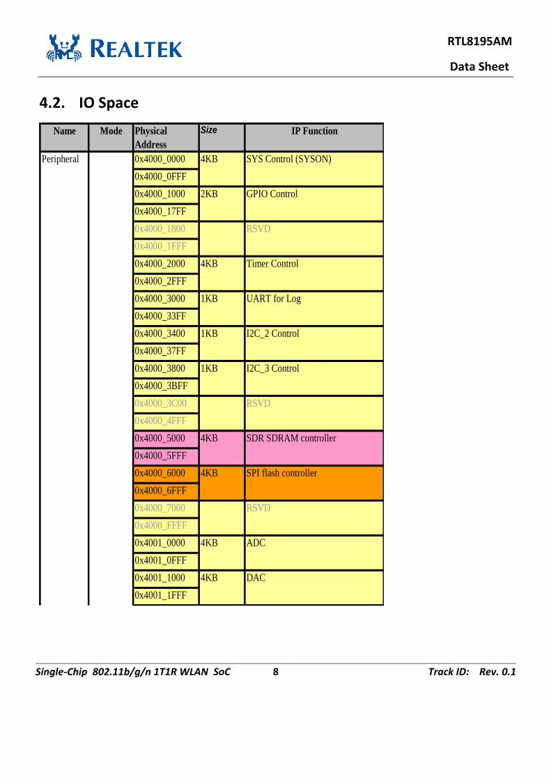
5. Pin Assignments
A1
B1
C1
D1
E1
F1
G1
H1
J1
K1
A2
C2
D2
E2
F2
G5
H2
J2
K4
A3
B3
C3
E4
H3
K3
A4
B4
C4
F4
H4
J4
A5
B5
C5
F3
J5
K5
A6
B6
C7
E6
J6
K6
B7
D7
J7
K7
A8
B8
E7
H8
J8
K8
A9
B9
C9
D9
E9
F9
G9
J9
K9
A10
B10
C10
D10
E10
F10
G10
H10
J10
K10
6m
m
6mm
Total 96 Balls
A11
B11
C11
D11
E11
F11
G11
H11
J11
K11
L11L1 L2 L3 L4 L5 L6 L7 L8 L9 L9
A7
B2
G6
Figure 4. Ball Assignments

RTL8195AM
Data Sheet
Single-Chip 802.11b/g/n 1T1R WLAN SoC 14 Track ID: Rev. 0.1
5.1. Package Identification
The version is shown in the location marked ‘VV’ in Figure 4, e.g., A0=Version A0

RTL8195AM
Data Sheet
Single-Chip 802.11b/g/n 1T1R WLAN SoC 15 Track ID: Rev. 0.1
5.2. Pin Descriptions
The following signal type codes are used in the tables:
I: Input O: Output
T/S: Tri-State bi-directional input/output pin S/T/S: Sustained Tri-State
O/D: Open Drain P: Power pin
5.2.1. Power-On Trap Pin
Table 1. Power On Trap Pins
Symbol Type Pin No Description
NORMAL_MODE_SEL I A3 Shared with GPIOB_2
1: Normal operation mode
0: Enter into test/debug mode
SPS_LDO_SEL I H8 Shared with GPIOF_4
0: Internal switching regulator select
1: Internal LDO select
BOOT_SCENARIO I B2 Shared with GPIOB_0
0: booting from flash
1: booting from internal memory
EEPROM_SEL I G9 Shared with GPIOF_5
0: Internal NV memory select
1: reserved for internal testing use
SD_DEV_SEL I E7 Shared with GPIOA_7
Weak Pull High: SDMMC Host mode
Weak Pull Low: SDIO device mode

RTL8195AM
Data Sheet
Single-Chip 802.11b/g/n 1T1R WLAN SoC 16 Track ID: Rev. 0.1
Symbol Type Pin No Description
ICFG0 I B6 Shared with GPIOC_0
When NORMAL_MODE_SEL is “0”, then ICFG0 is test mode BIT0.
ICFG1 I B7 Shared with GPIOC_1
When NORMAL_MODE_SEL is “0”, then ICFG1 is test mode BIT1.
ICFG2 I B8 Shared with GPIOC_2
When NORMAL_MODE_SEL is “0”, then ICFG2 is test mode BIT2.
ICFG3 I B9 Shared with GPIOC_3
When NORMAL_MODE_SEL is “0”, then ICFG3 is test mode BIT3.
5.2.2. Analog to DC Converter
Table 2. ADC Pins
Symbol Type Pin No Description
ADC_CH1 I L8 AD converter input channel 1
ADC_CH2 I L9 AD converter input channel 2
CAP_ADC P K8 Capacitor for AD converter power.
5.2.3. Digital to Analog Converter
Table 3. DAC Pins
Symbol Type Pin No Description
DAC_CH0 O L10 DA converter output channel 0
CAP_DAC P K9 Capacitor for DA converter power.

RTL8195AM
Data Sheet
Single-Chip 802.11b/g/n 1T1R WLAN SoC 17 Track ID: Rev. 0.1
5.2.4. RF and NFC
Table 4. RF and NFC Pins
Symbol Type Pin No Description
NFC_IP I C2 NFC input differential signal
NFC_IN I D1 NFC input differential signal
RF_IO IO L1 WL RF signal
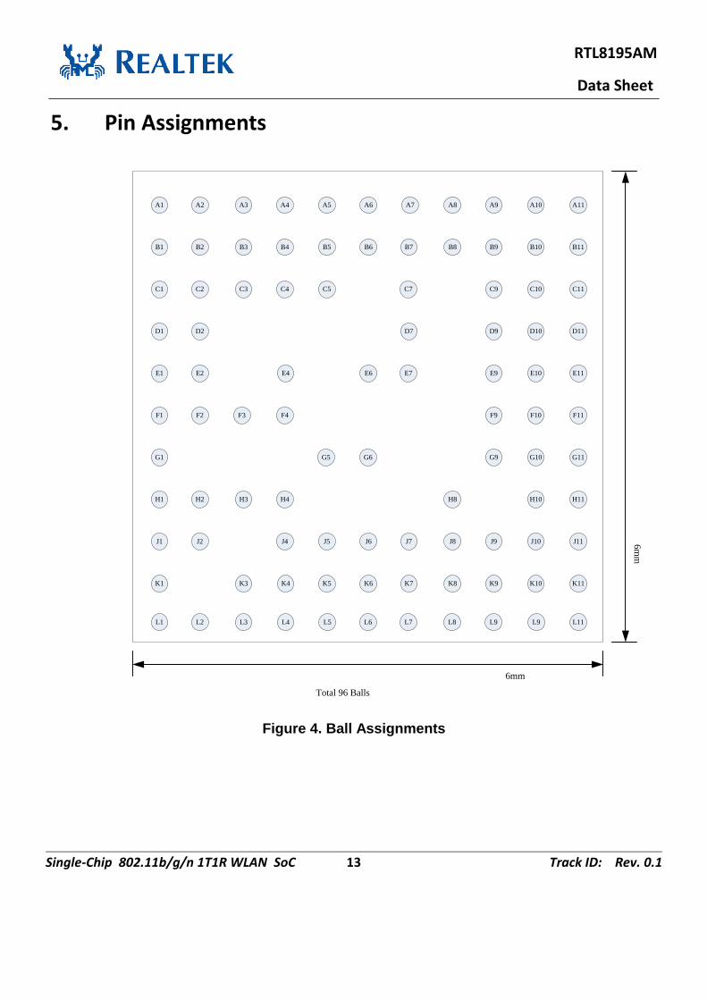
5.2.5. Power Pins
Table 5. Power Pins
Symbol Type Pin No Description
SW_LX P A11 Switching Regulator Output 1.2V
SW_HV3 P B11 Switching Regulator Input
Or Linear Regulator input from 3.3V to 1.2V
VA33 P C1, F1, G1, K1, L3, L11, D11
3.3V for Analog Circuit power source
VD33IO P A1 VDD3.3V for Digital IO power input
VD33_IN P A8 3.3V power input for digital blocks
VDD_IO P G11, L5 VDIO_A (G11) is power source for GPIOA group. The voltage level can be 1.8V ~ 3.3V.
VDIO_ED (L5) is power source for GPIOE and GPIOD group. The voltage level can be 1.8V ~ 3.3V.
VDD_IO P A5, C10 VDD_IO for memory and it’s IOs.
The voltage level is from 2.5V ~ 3.3V.
It is recommended that the power is provided from integrated LDO outputted from VDD_SRC (A9).
RTL8195AM
Data Sheet
Single-Chip 802.11b/g/n 1T1R WLAN SoC 18 Track ID: Rev. 0.1
Symbol Type Pin No Description
VD12D P A6, C11, E11, L7 1.2V power for digital circuits
VA12 P E1, H1, J1, L4 1.2V for analog blocks
VDD_SRC P A9 Integrated LDO output, voltage level from 1.8 ~ 2.7V.
VDD33_SRC P A7 Integrated power switch to output fixed 3.3V. SW controllable.
SW_GND P A10 Switching Regulator Ground
GND_LDO_SPS P B10 Switching Regulator ground
GND_CORE/ GND_IO
P C4, C5, C7, C9, D7, E4, E9, F4,
H4
Digital core ground and IO groud
NFC Ground P C3, D2, F3 NFC and analog ground
Analog Ground P H2, H3, J2, J7, J8, K3, L2
Analog ground
5.2.6. Clock Pins
Table 6. Clock and Other Pins
Symbol Type Pin No Description
XI I F2 40MHz OSC Input
Input of 40MHz Crystal Clock Reference
XO O E2 Output of 40MHz Crystal Clock Reference

RTL8195AM
Data Sheet
Single-Chip 802.11b/g/n 1T1R WLAN SoC 19 Track ID: Rev. 0.1
5.2.7. NOR Flash Interface
Table 7. NOR Flash Pins
Symbol Type Pin No Description
SPI_M_CLK IO K10 NOR Flash CLK signal. Multiplexed with GPIOF_1 .
SPI_M_DATA0 IO K11 NOR Flash CLK signal. Multiplexed with GPIOF_2 .
SPI_M_CS IO J10 NOR Flash CLK signal. Multiplexed with GPIOF_0 .
SPI_M_DATA1 IO J9 NOR Flash CLK signal. Multiplexed with GPIOF_3 .
5.2.8. Digital IO Pins
Please refer to section 6 Pin Function Table for more detailed information.
Table 8. Digital IO Pins
Symbol Type Pin No Description
CHIP_EN I J6 Whole chip enable control. When asserted, chip function is enabled; when de-asserted, whole chip is shutdown.
GPIOB_0 IO B2 GPIO pin. The MUX function can be referred to Pin Function Table.
GPIOB_1 IO B3 GPIO pin. The MUX function can be referred to Pin Function Table.
GPIOB_2 IO A3 GPIO pin. The MUX function can be referred to Pin Function Table.
GPIOB_3 IO A4 GPIO pin. The MUX function can be referred to Pin Function Table.
GPIOB_4 IO B1 GPIO pin. The MUX function can be referred to Pin Function Table.
GPIOB_5 IO A2 GPIO pin. The MUX function can be referred to Pin Function Table.

RTL8195AM
Data Sheet
Single-Chip 802.11b/g/n 1T1R WLAN SoC 20 Track ID: Rev. 0.1
Symbol Type Pin No Description
GPIOE_0 IO K7 GPIO pin. The MUX function can be referred to Pin Function Table.
GPIOE_1 IO L6 GPIO pin. The MUX function can be referred to Pin Function Table.
GPIOE_2 IO K6 GPIO pin. The MUX function can be referred to Pin Function Table.
GPIOE_3 IO K5 GPIO pin. The MUX function can be referred to Pin Function Table.
GPIOE_4 IO K4 GPIO pin. The MUX function can be referred to Pin Function Table.
GPIOE_5 IO J4 GPIO pin. The MUX function can be referred to Pin Function Table.
GPIOD_4 IO E6 GPIO pin. The MUX function can be referred to Pin Function Table.
GPIOD_5 IO G5 GPIO pin. The MUX function can be referred to Pin Function Table.
GPIOD_6 IO G6 GPIO pin. The MUX function can be referred to Pin Function Table.
GPIOD_7 IO J5 GPIO pin. The MUX function can be referred to Pin Function Table.
GPIOA_0 IO J11 GPIO pin. The MUX function can be referred to Pin Function Table.
GPIOA_1 IO H11 GPIO pin. The MUX function can be referred to Pin Function Table.
GPIOA_2 IO H10 GPIO pin. The MUX function can be referred to Pin Function Table.
GPIOA_3 IO G10 GPIO pin. The MUX function can be referred to Pin Function Table.
GPIOA_4 IO F11 GPIO pin. The MUX function can be referred to Pin Function Table.
GPIOA_5 IO F10 GPIO pin. The MUX function can be referred to Pin Function Table.

RTL8195AM
Data Sheet
Single-Chip 802.11b/g/n 1T1R WLAN SoC 21 Track ID: Rev. 0.1
GPIOA_7 IO E7 GPIO pin. The MUX function can be referred to Pin Function Table.
GPIOA_6 IO F9 GPIO pin. The MUX function can be referred to Pin Function Table.
GPIOC_0 IO B6 GPIO pin. The MUX function can be referred to Pin Function Table.
GPIOC_1 IO B7 GPIO pin. The MUX function can be referred to Pin Function Table.
GPIOC_2 IO B8 GPIO pin. The MUX function can be referred to Pin Function Table.
GPIOC_3 IO B9 GPIO pin. The MUX function can be referred to Pin Function Table.
GPIOC_4 IO B4 GPIO pin. The MUX function can be referred to Pin Function Table.
GPIOC_5 IO B5 GPIO pin. The MUX function can be referred to Pin Function Table.
5.2.9. USB Transceiver Interface
Table 9. USB Transceiver Interface
Symbol Type Pin No Description
HSDP IO D10 High-Speed USB D+ Signal
HSDM IO E10 High-Speed USB D- Signal
RREF P D9 Precision Resistor for Bandgap for USB interface

RTL8195AM
Data Sheet
Single-Chip 802.11b/g/n 1T1R WLAN SoC 22 Track ID: Rev. 0.1
5.2.10. SDMMC Interface
Table 10. SD/MMC Card Interface
Symbol Type Pin No Description
SD_D0 IO F11 SD/MMC Data 0. Multiplexed with GPIOA_4.
SD_D1 IO F10 SD/MMC Data 1. Multiplexed with GPIOA_5.
SD_D2 IO J11 SD/MMC Data 2. Multiplexed with GPIOA_0.
SD_D3 IO H11 SD/MMC Data 3. Multiplexed with GPIOA_1.
SD_CMD IO H10 SD/MMC Command. Multiplexed with GPIOA_2.
SD_CLK IO G10 SD/MMC Bus clock. Multiplexed with GPIOA_3.
SD_CD IO F9 SD/MMC Card Detection. Multiplexed with GPIOA_6.
SD_WT IO E7 SD/MMC Write Protection. Multiplexed with GPIOA_7.
5.2.11. SDIO Interface
Table 11 SDIO Device Interface
Symbol Type Pin No Description
SD_D0 IO F11 SDIO Data 0. Multiplexed with GPIOA_4.
SD_D1 IO F10 SDIO Data 1. Multiplexed with GPIOA_5.
SD_D2 IO J11 SDIO Data 2. Multiplexed with GPIOA_0.
SD_D3 IO H11 SDIO Data 3. Multiplexed with GPIOA_1.
SD_CMD IO H10 SDIO Command. Multiplexed with GPIOA_2.
SD_CLK IO G10 SDIO Bus clock. Multiplexed with GPIOA_3.

RTL8195AM
Data Sheet
Single-Chip 802.11b/g/n 1T1R WLAN SoC 23 Track ID: Rev. 0.1
6. Pin Function Table
6.1. Pin Configurable Function Group Summary Table
Table 12. Pin Function Group Table
PIN name JTAG SDD SDH MII UART Group I2C Group SPI Group I2S Group PCM Group WL_LED PWM ETE WKDT GPIO INT Default State SCHMTGPIOA_0 D2 D2 RX_CK UART2_IN SPI1_MISO GPIO_INT PH OGPIOA_1 D3 D3 RXD0 UART2_CTS SPI1_MOSI GPIO_INT HIGPIOA_2 CMD CMD RXD1 UART2_RTS SPI1_CLK PH OGPIOA_3 CLK CLK RXD2 UART0_RTS PH OGPIOA_4 D0 D0 RXD3 UART2_OUT SPI1_CS PHGPIOA_5 D1 D1 RXDV UART0_CTS D_SBY0 PHGPIOA_6 INT CD RXERR UART0_IN PHGPIOA_7 WP COL UART0_OUT HIGPIOB_0 LOG_OUT ETE0 D_SLP0 HIGPIOB_1 LOG_IN WL_LED0 ETE1 PHGPIOB_2 I2C3_SCL ETE2 HI OGPIOB_3 I2C3_SDA ETE3 GPIO_INT PHGPIOB_4 WL_LED0 PWM0 GPIO_INT PHGPIOB_5 WL_LED0 PWM1 PH OGPIOC_0 TXD2 UART0_IN SPI0_CS0 I2S1_WS PCM1_SYNC PWM0 ETE0 HIGPIOC_1 TXD1 UART0_CTS SPI0_CLK I2S1_CLK PCM1_CLK PWM1 ETE1 GPIO_INT HI OGPIOC_2 TXD0 UART0_RTS SPI0_MOSI I2S1_SD_TX PCM1_OUT PWM2 ETE2 HIGPIOC_3 TX_CK UART0_OUT SPI0_MISO I2S1_MCK PCM1_IN PWM3 ETE3 GPIO_INT HI OGPIOC_4 TXD3 I2C1_SDA SPI0_CS1 I2S1_SD_RX GPIO_INT HIGPIOC_5 TXEN I2C1_SCL SPI0_CS2 GPIO_INT HI OGPIOD_4 MDC UART2_IN I2C0_SDA SPI1_CS PCM1_SYNC PWM0 ETE0 GPIO_INT PH OGPIOD_5 MDIO UART2_CTS I2C0_SCL SPI1_CLK PCM1_CLK PWM1 ETE1 D_SBY2 GPIO_INT PH OGPIOD_6 UART2_RTS I2C1_SCL SPI1_MOSI I2S0_SD_RX PCM1_OUT PWM2 ETE2 GPIO_INT PH OGPIOD_7 UART2_OUT I2C1_SDA SPI1_MISO PCM1_IN PWM3 ETE3 GPIO_INT PH OGPIOE_0 TRST UART0_OUT I2C2_SCL SPI0_CS0 I2S0_WS PCM0_SYNC PWM0 PH OGPIOE_1 TDI UART0_RTS I2C2_SDA SPI0_CLK I2S0_CLK PCM0_CLK PWM1 GPIO_INT PH OGPIOE_2 TDO UART0_CTS I2C3_SCL SPI0_MOSI I2S0_SD_TX PCM0_OUT PWM2 GPIO_INT PH OGPIOE_3 TMS UART0_IN I2C3_SDA SPI0_MISO I2S0_MCK PCM0_IN PWM3 D_SBY3 GPIO_INT PH OGPIOE_4 CLK I2C3_SCL SPI0_CS1 PH OGPIOE_5 I2C3_SDA SPI0_CS2 GPIO_INT PH OGPIOF_4 HIGPIOF_5 HI NOTE1: PH = Pull-High, HI = High-impedance NOTE2: GPIOA_1 needs external Circuit to do the pull high control; others’ pull control can be done by register setting
(including GPIOA_1’s PD).
6.2. Notes on Pin Function
6.2.1. WKDT_DSLP Usage
WKDT_DSLP is wakeup pin for deep sleep state. This function can be enabled via API.

RTL8195AM
Data Sheet
Single-Chip 802.11b/g/n 1T1R WLAN SoC 24 Track ID: Rev. 0.1
6.2.2. WKDT_DSBY Usage
WKDT_DSBY is wakeup pin for deep standby state. This function can be enabled via API.
6.2.3. ETE Pin Usage
External trigger by GTimer. Gtimer can be configured with a specific timing to issue trigger event.

RTL8195AM
Data Sheet
Single-Chip 802.11b/g/n 1T1R WLAN SoC 25 Track ID: Rev. 0.1
7. Functional Description
7.1. Power Management Control Unit
7.1.1. Features
The PMU provides the following functions:
Bulk/LDO to output 1.2V
LDO to output 1.8V ~ 2.5V power source
Integrated power cut to output Vref (input from VD33_IN) with SW controllable
2 very Low power clock source with less accuracy: 1K Hz and 500K Hz
1 low power 32.768KHz clock source with moderate accuracy
Wakeup system detector to resume from low power state

RTL8195AM
Data Sheet
Single-Chip 802.11b/g/n 1T1R WLAN SoC 26 Track ID: Rev. 0.1
7.1.2. Power Mode Description
7.1.2.1 Shutdown Mode
CHIP_EN deasserts to shutdown whole chip without external power cut components required.
PMC TIM
IO
Detect
3.3V
IO PowerMCU
deassert
CHIP_EN
7.1.2.2 Deep Sleep Mode
CHIP_EN keeps high. Enter into Deep Sleep mode by API. The trigger timer period can be configured or
GPIOB_1 can be used as external trigger event. The DLSP trigger timer can be configured with the range
1 ~ 3600 sec.

RTL8195AM
Data Sheet
Single-Chip 802.11b/g/n 1T1R WLAN SoC 27 Track ID: Rev. 0.1
PMC TIM
IO
Detect
3.3V
IO (Wakeup)MCU
Keep High
CHIP_EN
Command
API to
Configure
TO (Wakeup)
7.1.2.3 Deep Standby Mode
CHIP_EN keeps high. Entering into Deep Sleep mode by API. The trigger timer period can be configured
or all GPIO group can be used as external trigger event.
PMC TIM
IO
Detect
3.3V
IOMCU
Keep High
CHIP_EN
Command

RTL8195AM
Data Sheet
Single-Chip 802.11b/g/n 1T1R WLAN SoC 28 Track ID: Rev. 0.1
7.2. Memory System
7.2.1. Memory Architecture
RTL8195AM integrates ROM, internal SRAM, extended SDR DRAM, extended NOR flash to provide
applications with a variety of memory requirements.
7.2.2. Internal ROM
RTL8195AM integrates 1MB ROM to provide high access speed, low leakage memory. The ROM
memory clock speed is up to 166MHz. The ROM lib provides the following functions:
Boot Code and MCU initialization
Default UART driver
Non-flash booting functions and drivers
Peripheral libs
Security function libs
7.2.3. Internal SRAM
448KB SRAM is integrated to provide instruction, data, and buffer usage. The maximum clock speed is
up to 166MHz.
Additional 64KB fast access data memory (TCM) is provided for FW data section. The range is
0x1FFF-0000 ~ 0x1FFF-FFFF.
7.2.4. Extended SDR DRAM
7.2.4.1 Features
Interface (Bus Width): 16-bit

RTL8195AM
Data Sheet
Single-Chip 802.11b/g/n 1T1R WLAN SoC 29 Track ID: Rev. 0.1
Targeted SDR Frequency: Up to 83MHz
Supports one Chip Select (MCS0#) and 1 Band select (BA0)
7.2.5. SPI NOR Flash
7.2.5.1 Features
Targeted SPI flash frequency: Up to 83.3MHz (when CPU clock is 166MHz)
In addition to a programmed I/O interface, also supports a memory-mapped I/O interface for read
operation
Supports Read and Fast Read in memory-mapped I/O mode
7.2.5.2 Supported NOR Flash List
Table 13. Flash Bus DC Parameters
Vendor Part Number Density Voltage IO
MXIC MXIC_MX25L4006E 4M Bits 3.3V 1I/2O
MXIC MXIC_MX25L8073E 8M Bits 3.3V 1I/2O
MXIC MXIC_MX25L8006E 8M Bits 3.3V 1I/2O
MXIC MXIC_MX25L16006E 16M Bits 3.3V 1I/2O
7.2.5.3 Electrical Specifications
Table 14. Flash Bus DC Parameters
Symbol Parameter Conditions Min. Typ. Max. Units Notes
VIH Input-High Voltage LVTTL 2.0 - - V 1

RTL8195AM
Data Sheet
Single-Chip 802.11b/g/n 1T1R WLAN SoC 30 Track ID: Rev. 0.1
Symbol Parameter Conditions Min. Typ. Max. Units Notes
VIL Input-Low Voltage LVTTL - - 0.8 V 2
VOH Output-High Voltage - 2.4 - - V 3
VOL Output-Low Voltage - - - 0.4 V 3
IIL Input-Leakage Current VIN=3.3V or 0 -10 1 10 A -
IOZ Tri-State Output-Leakage Current
- -10 1 10 A -
RPU Input Pull-Up Resistance - - 75 - KΩ 4
RPD Input Pull-Down Resistance - - 75 - KΩ 4
Note 1: VIH overshoot: VIH (MAX)=VDDH + 2V for a pulse width 3ns.
Note 2: VIL undershoot: VIL (MIN)=-2V for a pulse width 3ns.
Note 3: The output current buffer is 8mA for the flash address and data bus; and is 8mA for Flash control signals.
Note 4: These values are typical values checked in the manufacturing process and are not tested.
7.3. General Purpose DMA Controller
7.3.1. Features of GDMA
Dual port DMA with totally 12 channels
Configurable endian
Support memory-memory, memory-peripheral, peripheral-memory, and peripheral-peripheral DMA
transfer
Support block level flow control
Support address auto-reload, link-listed mode
Support scatter-gather mode

RTL8195AM
Data Sheet
Single-Chip 802.11b/g/n 1T1R WLAN SoC 31 Track ID: Rev. 0.1
7.4. General Purpose Timer
7.4.1. Features of GTimer
8 Gtimer supported
Source clock is 32.768KHz
Support Counter mode and timer mode
7.5. GPIO Functions
7.5.1. Features of GPIO
GPO and GPI function
Support interrupt detection with configurable polarity per GPIO
Internal weak pull up and pull low per GPIO
Multiplexed with other specific digital functions
7.6. UART Interface Characteristics
7.6.1. Features of UART
Support maximum 2 HS-UART (max baud rate 4MHz and DMA mode) and 2 low speed UART (IO
mode)
UART (RS232 Standard) Serial Data Format
Transmit and Receive Data FIFO
Programmable Asynchronous Clock Support
Auto Flow Control

RTL8195AM
Data Sheet
Single-Chip 802.11b/g/n 1T1R WLAN SoC 32 Track ID: Rev. 0.1
Programmable Receive Data FIFO Trigger Level
DMA data moving support to save CPU loading
7.6.2. High Speed UART Specification
The RTL8195AM UART interface is a standard 4-wire interface with RX, TX, CTS, and RTS. The default
baud rate is 115.2k baud. In order to support high and low speed baud rate, the RTL8195AM provides
multiple UART clocks.
Table 15. UART Baud Rate Specifications
Desired Baud Rate
Actual Baud Rate
Error (%)
300 300 0.00%
600 600 0.00%
900 900 0.00%
1200 1200 0.00%
1800 1800 0.00%
2400 2400 0.00%
3600 3601 0.03%
4800 4798 -0.04%
7200 7198 -0.03%
9600 9603 0.03%
14400 14395 -0.03%
19200 19182 -0.09%
28800 28846 0.16%
38400 38462 0.16%
56000 55970 -0.05%
57600 57692 0.16%
76800 76531 -0.35%
Desired Baud Rate
Actual Baud Rate
Error (%)
115200 115385 0.16%
128000 127119 -0.69%
153600 153061 -0.35%
230400 229167 -0.54%
460800 458333 -0.54%
500000 500000 0.00%
921600 916667 -0.54%
1000000 1000000 0.00%
1382400 1375000 -0.54%
1444444 1437500 -0.48%
1500000 1500000 0.00%
1843200 1833333 -0.54%
2000000 2000000 0.00%
2100000 2083333 -0.79%
2764800 2777778 0.47%
3000000 3000000 0.00%
3250000 3250000 0.00%

RTL8195AM
Data Sheet
Single-Chip 802.11b/g/n 1T1R WLAN SoC 33 Track ID: Rev. 0.1
Desired Baud Rate
Actual Baud Rate
Error (%)
3692300 3703704 0.31%
3750000 3750000 0.00%
Desired Baud Rate
Actual Baud Rate
Error (%)
4000000 4000000 0.00%

RTL8195AM
Data Sheet
Single-Chip 802.11b/g/n 1T1R WLAN SoC 34 Track ID: Rev. 0.1
Figure 5. UART Interface Waveform
7.6.3. UART Interface Signal Levels
The UART signal level ranges from 1.8V to 3.3V. The host provides the power source with the targeted
power level to the RTL8195AM UART interface via the IO power.
7.7. SPI Interface
7.7.1. Features of SPI
Support maximum 2 SPI port
Support Master/Slave mode (SPI0 only), and Master only (SPI1)
Support DMA to offload CPU bandwidth
1 very high speed SPI (Master only)
Support up to 3 CS (multi-slave mode up to 3 slave)
Support baud rate up to 41MHz (Master mode)
1 high speed SPI (Master/Slave)

RTL8195AM
Data Sheet
Single-Chip 802.11b/g/n 1T1R WLAN SoC 35 Track ID: Rev. 0.1
Support baud rate up to 20MHz (Master mode)
Support baud rate up to 5MHz (Slave mode Rx only)
Support baud rate up to 4MHz (Slave mode TRx)
Programmable clock bit-rate
Programmable clock polarity and phase
Multiple Serial Interface Operations support
Motorola - SPI
Texas Instruments - SSI
National Semiconductor - Microwire
7.8. I2C Interface
7.8.1. Features of I2C
Support maximum 4 I2C port
Three speeds:
Standard mode (0 to 100 Kb/s)
Fast mode (<400 Kb/s)
High-speed mode (<3.4 Mb/s) (with appropriate bus loading)
Master or Slave I2C operation
7- or 10-bit addressing
Transmit and receive buffers
TX and RX DMA support (I2C 0 and 1 only)

RTL8195AM
Data Sheet
Single-Chip 802.11b/g/n 1T1R WLAN SoC 36 Track ID: Rev. 0.1
7.9. PWM Interface
7.9.1. Features of PWM
Support maximum 4 PWM functions
0~100% duty can be configurable
Minimum resolution is 64us
The period can be configured up to 8 seconds
7.10. External Trigger Event Interface
7.10.1. Features of External Trigger Event
Support maximum 4 External Trigger Event functions without CPU active
Triggered by GTIMER
7.11. USB Device v2.0 Interface
7.11.1. Features USB Device Interface
Support HS/FS/LS modes
Up to 4 Endpoints in addition to Endpoint 0 (2 In-Endpoint and 2 Out-Endpoint)
Support bulk, interrupt, and isochronous transfer
Support suspend, Resume and remote wakeup operation
Internal DMA support
Support non-flash booting in the use of Ethernet to WIFI transformation card

RTL8195AM
Data Sheet
Single-Chip 802.11b/g/n 1T1R WLAN SoC 37 Track ID: Rev. 0.1
7.12. USB Host Interface
7.12.1. Features of USB Host Interface
Support HS/FS/LS modes
Support up to 8 host channels
Automatic ping capabilities
Support Split transfers
Suspend, Resume and remote wakeup operation
Internal DMA support
7.12.2. Electrical Specifications
Table 16. USB v2.0 DC Parameters
Symbol Parameter Conditions Min. Typ. Max. Units Notes
VIH Input-High Voltage - 200 - - mV 2
VIL Input-Low Voltage - - - 10 mV 2
VOH Output-High Voltage - 300 - 500 mV 2
VOL Output-Low Voltage - -10 - 10 mV 2
IIL Input-Leakage Current - - - - A 1
Note 1: These values are typical values checked in the manufacturing process and are not tested.
Note 2: For additional information, see the USB v2.0 Specification.

RTL8195AM
Data Sheet
Single-Chip 802.11b/g/n 1T1R WLAN SoC 38 Track ID: Rev. 0.1
7.13. SDIO/RTK SPI Device Mode Interface
7.13.1. Features of SDIO/RTK SPI Device Mode Interface
Support SDIO 2.0 SDR25
CIS can be configured with internal non-volatile memory for fast card detection
RTK SPI provides high efficiency SPI interface with interrupt and full duplex mode
Support high performance Ethernet to WIFI transformation
Support non-flash booting in the use of Ethernet to WIFI transformation card
7.13.2. SDIO Device Mode Specifications
7.13.2.1 Bus Timing Specification
TWL TWH
fPP
TISU TIH
TODLY
Clock
Input
Output
Figure 6. SDIO Interface Timing
Table 17. SDIO Interface Timing Parameters
NO Parameter Mode MIN MAX Unit
fPP Clock Frequency Default 0 25 MHz
HS 0 50 MHz

RTL8195AM
Data Sheet
Single-Chip 802.11b/g/n 1T1R WLAN SoC 39 Track ID: Rev. 0.1
NO Parameter Mode MIN MAX Unit
TWL Clock Low Time DEF 10 - ns
HS 7 - ns
TWH Clock High Time DEF 10 - ns
HS 7 - ns
TISU Input Setup Time DEF 5 - ns
HS 6 - ns
TIH Input Hold Time DEF 5 - ns
HS 2 - ns
TODLY Output Delay Time DEF - 14 ns
HS - 14 ns
7.14. MII Interface
The MII interface can support both PHY/MAC mode.
Supports 10/100Mbps operation
Supports half/full duplex operation
IEEE 802.3/802.3u compliant
Auto negotiation
TX and RX separated
TRx FIFO 2K bytes
7.15. I2S Interface Characteristics
7.15.1. Features of I2S
Support 8/16/24/32/48/96KHz, 44.1/88.2KHz

RTL8195AM
Data Sheet
Single-Chip 802.11b/g/n 1T1R WLAN SoC 40 Track ID: Rev. 0.1
Support 16 or 24 bits format
Integrated DMA engine to minimize SW efforts
Support TX and RX direction
Master or Slave mode support
7.16. PCM Interface Characteristics
7.16.1. Features of PCM
The RTL8195AM supports a PCM digital audio interface that is used for transmitting digital audio/voice
data to/from the Audio Codec. Features are supported as below:
Supports Master and Slave mode
Programmable long/short Frame Sync
Supports 8-bit A-law/µ-law, and 13/16-bit linear PCM formats
Supports sign-extension and zero-padding for 8-bit and 13-bit samples
Supports padding of Audio Gain to 13-bit samples
PCM Master Clock Output: 64, 128, 256, or 512kHz
Supports SCO/ESCO link
7.16.2. PCM Specifications
7.16.2.1 PCM Format
FrameSync is the synchronizing function used to control the transfer of DAC_Data and ADC_Data. A
Long FrameSync indicates the start of ADC_Data at the rising edge of FrameSyn, and a Short FrameSync
indicates the start of ADC_Data at the falling edge of FrameSync.

RTL8195AM
Data Sheet
Single-Chip 802.11b/g/n 1T1R WLAN SoC 41 Track ID: Rev. 0.1
BCLK
FrameSync
DAC_Data
ADC_Data
Figure 7. Long FrameSync
BCLK
FrameSync
DAC_Data
ADC_Data
Figure 8. Short FrameSync
7.16.2.2 Sign Extension and Zero Padding for 8-Bit and 13-Bit Samples
For 16-bit linear PCM output, 3 or 8 unused bits may be sign extended/zero padded.
21 43 65 87 109 1211 1413 1615DAC_Data
Sign Extension 8-bit PCM sample data
Figure 9. 16-Bit Output Data with 8-Bit PCM Sample Data and Sign Extension
21 43 65 87 109 1211 1413 1615DAC_Data
Zero Padding8-bit PCM sample data
Figure 10. 16-Bit Output Data with 8-Bit PCM Sample Data and Zero Padding

RTL8195AM
Data Sheet
Single-Chip 802.11b/g/n 1T1R WLAN SoC 42 Track ID: Rev. 0.1
21 43 65 87 109 1211 1413 1615DAC_Data
13-bit PCM sample dataSign Extension
Figure 11. 16-Bit Output Data with 13-Bit PCM Sample Data and Sign Extension
For 16-bit linear PCM output, 3-bit programmable audio gain value can be padded to 13-bit sample
data.
21 43 65 87 109 1211 1413 1615DAC_Data
Audio Gain13-bit PCM sample data
Figure 12. 16-Bit Output Data with 13-Bit PCM Sample Data and Audio Gain
7.16.2.3 PCM Interface Timing
FrameSync
BCLK
DAC_Data
FBCLK
TBCLKH TBCLKL
TFrameSync_Delay
TBCLKD_OUT
DAC_Data
TSETUPIN THOLDIN
MSB(LSB) LSB(MSB)
MSB(LSB) LSB(MSB)

RTL8195AM
Data Sheet
Single-Chip 802.11b/g/n 1T1R WLAN SoC 43 Track ID: Rev. 0.1
Figure 13. PCM Interface (Long FrameSync)
FrameSync
BCLK
DAC_Data
FBCLK
TBCLKH TBCLKL
TFrameSync_Delay
TBCLKD_OUT
DAC_Data
TSETUPIN THOLDIN
MSB(LSB) LSB(MSB)
MSB(LSB) LSB(MSB)
Figure 14. PCM Interface (Short FrameSync)
Table 18. PCM Interface Clock Specifications
Symbol Description Min. Typ. Max. Unit
FBCLK Frequency of BCLK (Master) 64 - 512 kHz
FFrameSync Frequency of Frame Sync (Master) - 8 - kHz
FBCLK Frequency of BCLK (Slave) 64 - 512 kHz
FFrameSync Frequency of Frame Sync (Slave) - 8 - kHz
D Data Size 8 8 16 bits
N Number of Slots Per Frame 1 1 1 Slots

RTL8195AM
Data Sheet
Single-Chip 802.11b/g/n 1T1R WLAN SoC 44 Track ID: Rev. 0.1
Table 19. PCM Interface Timing
Symbol Description Min. Typ. Max. Unit
TBCLKH High Period of BCLK 980 - - ns
TBCLKL Low Period of BCLK 970 - - ns
TFrameSync_Del
ay
Delay Time from BCLK High to Frame Sync High
- - 75 ns
TBCLKD_OUT Delay Time from BCLK High to Valid DAC_Data
- - 125 ns
TSETUPIN Set-up Time for ADC_Data Valid to BCLK Low
10 - - ns
THOLDIN Hold Time for BCLK Low to ADC_Data Invalid
125 - - ns
7.16.2.4 PCM Interface Signal Levels
The PCM signal level ranges from 1.8V to 3.3V. The host provides the power source with the targeted
power level to the RTL8711AM PCM interface via the VDD_IO pin.
7.17. AD Converter
7.17.1. Features
Up to 2 sets of 12-bit resolution A/D converter channel configurable
Bandwidth 4KHz
Input signal range: 0.01V ~ VREF - 0.2V
1 16-bit high resolution A/D converter (ADC_CH2 only)
Bandwidth 48KHz

RTL8195AM
Data Sheet
Single-Chip 802.11b/g/n 1T1R WLAN SoC 45 Track ID: Rev. 0.1
Input signal range: 0.01V ~ VREF - 0.2V
Support DMA mode
Support One-Shot sampling mode without CPU active to save power
Pre-configured period to auto-sampling
Support two wakeup method: buffer threshold interrupt and event trigger
7.18. DA Converter
7.18.1. Features
Up to 2 sets of 12-bit resolution D/A converter channel configurable
Bandwidth 16KHz
Output signal range: 0.01V ~ VREF - 0.2V
Support DMA mode
7.19. Security Engine
7.19.1. Features
Provide low SW computing and high performance encryption
Supported authentication algorithms:
MD5
SHA-1

RTL8195AM
Data Sheet
Single-Chip 802.11b/g/n 1T1R WLAN SoC 46 Track ID: Rev. 0.1
SHA-2 (SHA-224 / SHA-256 )
HMAC-MD5
HMAC-SHA1
HMAC-SHA2
Supported Encryption / Decryption mechanisms:
DES ( CBC / ECB )
3DES ( CBC / ECB )
AES-128 ( CBC / ECB / CTR )
AES-192 ( CBC / ECB / CTR )
AES-256 ( CBC / ECB / CTR )

RTL8195AM
Data Sheet
Single-Chip 802.11b/g/n 1T1R WLAN SoC 47 Track ID: Rev. 0.1
8. Electrical Characteristics
8.1. Temperature Limit Ratings
Table 20. Temperature Limit Ratings
Parameter Minimum Maximum Units
Storage Temperature -55 +125 C
Ambient Operating Temperature -20 +85 C
Junction Temperature 0 +125 C
8.2. Temperature Characteristics
Table 21. Thermal Properties
Power (w) PCB (layer) Theta ja (C/W) Theta jc (C/W) Psi jt (C/W)
1 2 122.1 15 1.31
1 4 42.3 12.5 0.36
8.3. Power Supply DC Characteristics
Table 22. Power Supply DC Characteristics
Symbol Parameter Minimum Typical Maximum Units
VA33, VD33IO, SW_HV3
3.3V Supply Voltage 3.0 3.3 3.6 V
VDD_IO Digital IO Supply Voltage
1.62 1.8~3.3 3.6 V

RTL8195AM
Data Sheet
Single-Chip 802.11b/g/n 1T1R WLAN SoC 48 Track ID: Rev. 0.1
Symbol Parameter Minimum Typical Maximum Units
VA12_AFE, VA12_SYN, VA12_RF
1.2V Core Supply Voltage
1.08 1.2 1.32 V
IDD33 3.3V Rating Current (with internal regulator and integrated CMOS PA)
- - 450 mA
IDD_IO IO Rating Current (including VDD_IO)
200 mA
IDD_IO_33 3.3V IO Rating Current 50 mA
8.4. Power State and Power Consumptions
8.4.1. Power Mode Description
Shutdown Mode
CHIP_EN deasserts to shutdown whole chip without external power cut components required.

RTL8195AM
Data Sheet
Single-Chip 802.11b/g/n 1T1R WLAN SoC 49 Track ID: Rev. 0.1
PMC TIM
IO
Detect
3.3V
IO PowerMCU
deassert
CHIP_EN
Deep Sleep Mode
CHIP_EN keeps high. Enter into Deep Sleep mode by API. The trigger timer period can be configured or
GPIOB_0 can be used as external trigger event. The DLSP trigger timer can be configured with the range
1 ~ 3600 sec.
PMC TIM
IO
Detect
3.3V
IO (Wakeup)MCU
Keep High
CHIP_EN
Command
API to
Configure
TO (Wakeup)

RTL8195AM
Data Sheet
Single-Chip 802.11b/g/n 1T1R WLAN SoC 50 Track ID: Rev. 0.1
Deep Standby Mode
CHIP_EN keeps high. Entering into Deep Sleep mode by API. The trigger timer period can be configured
or all GPIO group can be used as external trigger event.
PMC TIM
IO
Detect
3.3V
IOMCU
Keep High
CHIP_EN
Command
8.4.2. Power On Sequence (Power On or Resume from Deep Sleep)

RTL8195AM
Data Sheet
Single-Chip 802.11b/g/n 1T1R WLAN SoC 51 Track ID: Rev. 0.1
VDD_IO
CHIP_EN
1.2VTcore
Tboot
RCOTCLK
VDD SDRAM
VD33x3.3V
> 1.8V
Tmem
CPU boot time
Figure 15. Power-On Sequence or Resume from Deep Sleep
Table 23. Timing spec for power on sequence
Symbol Parameter Minimum Typical Maximum Units
TCLK Internal ring clock stable time after 3.3V ready
1 ms
Tcore Core power ready time 1.5 1.5 ms
Tboot 1.2V Core Supply Voltage
200 200 ms
Tmem: SW controlled memory power ready time.

RTL8195AM
Data Sheet
Single-Chip 802.11b/g/n 1T1R WLAN SoC 52 Track ID: Rev. 0.1
8.4.3. Resume from Deep Standby
1.8V ~ 3.3V
CHIP_EN
1.2VTcore
Tboot
Wake up by GPIO or Timer
VDD_IO
3.3VVD33x
CPU boot time
Figure 16. Timing Sequence resume from Deep Standby
8.5. Digital IO Pin DC Characteristics
8.5.1. Electrical Specifications
Table 24. Typical Digital IO DC Parameters (3.3V Case)
Symbol Parameter Conditions Min. Typ. Max. Units
VIH Input-High Voltage LVTTL 2.0 - - V
VIL Input-Low Voltage LVTTL - - 0.8 V
VOH Output-High Voltage LVTTL 2.4 - - V
VOL Output-Low Voltage LVTTL - - 0.4 V

RTL8195AM
Data Sheet
Single-Chip 802.11b/g/n 1T1R WLAN SoC 53 Track ID: Rev. 0.1
Symbol Parameter Conditions Min. Typ. Max. Units
VT+ Schmitt-trigger High Level 1.78 1.87 1.97 V
VT- Schmitt-trigger Low Level 1.36 1.45 1.56 V
IIL Input-Leakage Current VIN=3.3V or 0 -10 1 10 A
Table 25. Typical Digital IO DC Parameters (1.8V Case)
Symbol Parameter Conditions Min. Typ. Max. Units
VIH Input-High Voltage CMOS 0.65x VCC - - V
VIL Input-Low Voltage CMOS - - 0.35x VCC V
VOH Output-High Voltage CMOS VCC-0.45 - - V
VOL Output-Low Voltage CMOS - - 0.45 V
VT+ Schmitt-trigger High Level 1.02 1.09 1.14 V
VT- Schmitt-trigger Low Level 0.67 0.73 0.8 V
IIL Input-Leakage Current VIN=1.8V or 0 -10 1 10 A
8.6. USB Electrical Specifications
Table 26. USB v2.0 DC Parameters
Symbol Parameter Conditions Min. Typ. Max. Units Notes
VIH Input-High Voltage - 200 - - mV 2
VIL Input-Low Voltage - - - 10 mV 2
VOH Output-High Voltage - 300 - 500 mV 2
VOL Output-Low Voltage - -10 - 10 mV 2
IIL Input-Leakage Current - - - - A 1
Note 1: These values are typical values checked in the manufacturing process and are not tested.
Note 2: For additional information, see the USB v2.0 Specification.

RTL8195AM
Data Sheet
Single-Chip 802.11b/g/n 1T1R WLAN SoC 54 Track ID: Rev. 0.1
9. Mechanical Dimensions
9.1. Package Specification

RTL8195AM
Data Sheet
Single-Chip 802.11b/g/n 1T1R WLAN SoC 55 Track ID: Rev. 0.1
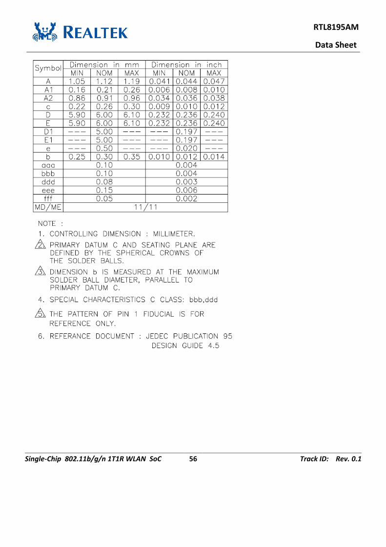
9.2. Mechanical Dimensions Notes
RTL8195AM
Data Sheet
Single-Chip 802.11b/g/n 1T1R WLAN SoC 56 Track ID: Rev. 0.1

RTL8195AM
Data Sheet
Single-Chip 802.11b/g/n 1T1R WLAN SoC 57 Track ID: Rev. 0.1
10. Ordering Information
Table 27. Ordering Information
Part Number Package Status
RTL8195AM-VB1-CG TFBGA96 MP
Note: See page 14 for package identification.