RTD2662/2660 series Flat Panel Display Controller -...
15
Realtek RTD2662/2660 series RTD2662/2660 series Flat Panel Display Controller
Transcript of RTD2662/2660 series Flat Panel Display Controller -...

Realtek RTD2662/2660 series
RTD2662/2660 series
Flat Panel Display Controller

Realtek RTD2662 series
2
1. Features General Embedded 3 DDC with DDC1/2B/CI Zoom scaling up and down Embedded one MCU with SPI flash controller. It contains 8 ADCs in D-connector,LED
backlight,and key pad application It supports infrared remote function Require only one crystal to generate all timing. Programmable internal low-voltage-reset (LVR) High resolution 6 channels PWM output, and
wide range selectable PWM frequency. Support input format up to
1920(WUXGA)/1440-pixel width(option) Analog RGB Input Interface 2 Analog input supported with internal switch Integrated 8-bit triple-channel 210/165MHz
ADC/PLL(option) Embedded programmable Schmitt trigger of
HSYNC Support Sync-On-Green (SOG) and various
kinds of composite sync modes On-chip high-performance hybrid PLLs High resolution true 64 phase ADC PLL Y/Pb/Pr support up to HDTV 1080p resolution
Embedded Video Decoder High performance AV 2D Comb-filter Support Composite, S Video, Component input Support VBI with Closed caption/ V chip slicer
Video Input Interface Support 8-bit video (ITU 656) format input
HDMI Digital Input Interface with HDCP (This function will be canceled in RTD2660) Dual HDMI Input with embedded high speed
switch Single link on-chip TMDS receiver Long cable support to 165Mhz Adaptive algorithm for TMDS capability Data enable only mode support High-Bandwidth Digital Content Protection
(HDCP 1.1) Enhanced protection of HDCP secret key CEC function supported Capable of 8-channel I2S/SPDIF output in
HDMI application Embedded MCU Industrial standard 8051 core with serial flash up
to 256K bytes Low speed ADC for various application Infrared function supported I2C Master or Slave hardware supported
Auto Detection /Auto Calibration Input format detection Compatibility with standard VESA mode and
support user-defined mode Smart engine for Phase/Image position/Color
calibration Scaling Fully programmable zoom ratios Independent horizontal/vertical scaling Advanced zoom algorithm provides high image
quality Sharpness/Smooth filter enhancement Support non-linear scaling from 4:3 to 16:9 or
16:9 to 4:3 Color Processor True 10 bits color processing engine sRGB compliance Advanced dithering logic for 18-bit panel color
depth enhancement Dynamic overshoot-smear canceling engine Brightness and contrast control Programmable 10-bit gamma support Peaking/Coring/XVYCC function for video
sharpness DLTI/DCTI/ Noise reduction for video quality
VividColorTM Independent color management (ICM) Dynamic contrast control (DCC)
Output Interface Fully programmable display timing generator Flexible data pair swapping for easier system
design. Programmable TCON function support 1 and 2 pixel/clock panel support and up to
170MHz, 1920/1440-pixel width(option) Multi-output interface (LVDS/ TTL)on single
PCB Spread-Spectrum DPLL to reduce EMI Fixed Last Line output for perfect panel
capability
Embedded OSD Embedded 16.5K SRAM dynamically stores
OSD command and fonts Support multi-color RAM font, 1, 2 and 4-bit per
pixel 16 color palette with 24bit true color selection Maximum 8 window with alpha-blending/
gradient /dynamic fade-in/fade-out, bordering/ shadow/3D window type
Rotary 90,180,270 degree
Realtek RTD2662 series
3
Independent row shadowing/bordering Programmable blinking effects for each character OSD-made internal pattern generator for factory
mode Support 12x18~4x18 proportional font Hardware decompression for OSD font Special function for closed-caption and CGMS
Power & Technology 3.3V / 1.8V power supply
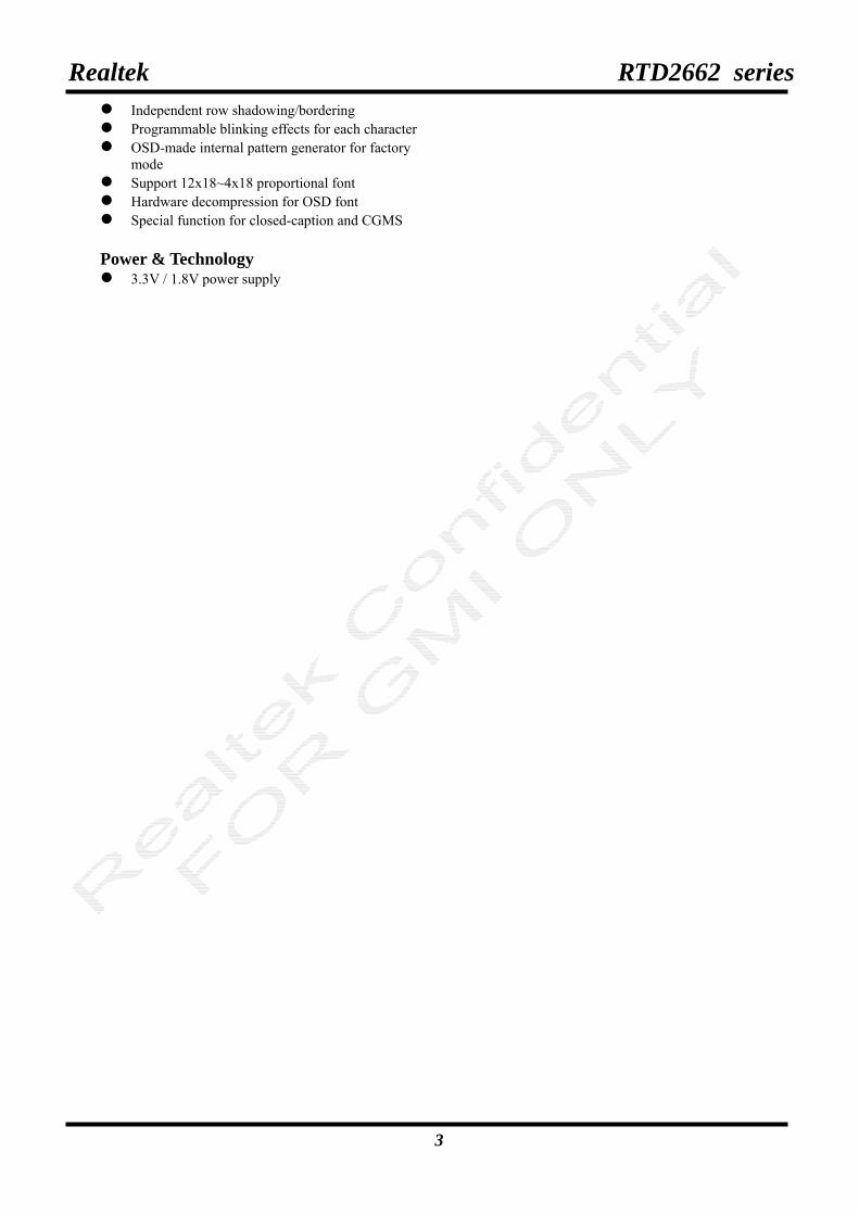
Realtek RTD2662
4
RTD2662
5251504948474645444342414039
3837363534333231302928272625242322212019181716151413121110987654321
ARED4/ARED6 /TXEC-
53 54 55 56 57 58 59 60 61 62 63 64
6566676869707172737475767778798081828384858687888990919293949596979899
100101102
103
104
ARED3/ARED5 / TXE2+
ARED7/AGRN3 /TXE3+ARED6/AGRN2 /TXE3-ARED5/ARED7 /TXEC+
ARED2/ARED4 / TXE2-ARED1/ARED3 /TXE1+ARED0/ARED2 /TXE1-DENA/TXE0+DHS/TXE0-
105
106
107
108
109
110
111
112
113
114
115
116
117
118
119
120
121
122
123
124
125
126
127
128
VA
DC
_VD
D
v8_7
/Vin
+0R
ESET
B
NC
DD
CSC
L2/G
PIO
XO
DD
CSD
A2/
GPI
O
XI
v8_0
/AH
S1V
CLK
/AV
S1
v8_6
/Vin
-0v8
_5/V
in+1
v8_4
/Vin
-1v8
_3/V
in+2
V8_
2/V
in-2
VC
CK
GN
DK
v8_1
/Vin
+3 NC
PVC
C
ABLU1/GPIO/ABLU7/TXO3+ABLU0/GPIO/ABLU6 / TXO3-AGRN7/GPIO/ABLU5 / TXOC+AGRN6/GPIO/ABLU4/ TXOC-AGRN5/GPIO/ABLU3 /TXO2+AGRN4/GPIO/ABLU2 /TXO2-AGRN3/GPIO/AGRN7 /TXO1+AGRN2/GPIO/AGRN6/TXO1-AGRN1/GPIO/AGRN5 /TXO0+AGRN0/GPIO/AGRN4/TXO0-
AHS0
v8_4/RX0P_0
AVS0
v8_7/RXCN_0v8_6/RXCP_0v8_5/RX0N_0
v8_0/ RX2P_0
v8_3/RX1N_0v8_2/RX1P_0v8_1/RX2N_0
TMDS_REXT
B0+G0-
R0-SOG0
G0+
B0-
ADC_GND/VADC_GND
R0+
TMDS_VDD
TMDS_GND
RX0P_1
RXCN_1RXCP_1RX0N_1
RX1N_1RX1P_1
RX2N_1
TMDS_VDD
RX2P_1
v8_6/B1+v8_5/G1-
v8_2/R1-v8_3/SOG1v8_4/G1+
v8_7/B1-
v8_1/R1+
ADC_VDD
v8_0
/Vin
-3
CEC DD
CSD
A3/
GPI
OD
DC
SCL3
/GPI
OV
CC
K
SD2/
SPD
IF2/
TCO
N[8
]/GPI
O/II
CSC
L/PW
M1
SPI_
SCLK
/SD
IO
CEB
/IRQ
B
SI/M
CU
_SC
LKSO
/SC
SB
MC
K/T
CO
N[7
]/GPI
OSC
K/T
CO
N[3
]/GPI
OW
S/TC
ON
[6]/G
PIO
SD3/SPDIF3/TCON[10]/GPIO/PWM0
SD0/
SPD
IF0/
TCO
N[4
]/GPI
OSD
1/SP
DIF
1/TC
ON
[9]/G
PIO
SD2/
SPD
IF2/
TCO
N[1
]/GPI
O/Ir
DA
SD3/
SPD
IF3/
TCO
N[1
3]/G
PIO
/VC
LK
SD0/
SPD
IF0/
TCO
N[9
]/GPI
OSD
1/SP
DIF
1/TC
ON
[5]/G
PIO
/IRQ
B/II
CSD
A
WS/TCON[7][1]/GPIO/PWM1
SD0/
SPD
IF0/
TCO
N[0
]/GPI
O/Ir
DA
B-A
DC
2/II
CSD
A/G
PIO
B-A
DC
1/II
CSC
L/G
PIO
BA
DC
0/PW
M1/
PWM
5/G
PIO
ABLU2/SPDIF3/SD3/TCON[10][8]/GPIO/PWM1/PWM5
GPIO/PWM2DVS/GPIO/PWM1DCLK/GPIO/PWM0
GPIO/PWM4/TCON[12][3]GPIO/PWM3/TCON[11][6]
GPIO/PWM5/TCON[0]
PVCCPGND
PVC
CPG
ND
ABLU3/SPDIF2/SD2/TCON[9][11]/GPIO/IICSDAABLU4/SPDIF1/SD1/TCON[7][3]/GPIO/IICSCLABLU5/SD0/SPDIF0/TCON[13][3]/GPIO
A-A
DC
0/A
VO
UT/
VC
LK/G
PIO
A-A
DC
1/G
PIO
A-A
DC
2/G
PIO
A-A
DC
3/G
PIO
A-A
DC
4/G
PIO
DD
CSC
L1/G
PIO
DD
CSD
A1/
GPI
O
ABLU6/MCK/TCON[5][9]/GPIOABLU7/SCK/TCON[4][2]/GPIO
NCVCCK
Realtek RTD2662
5
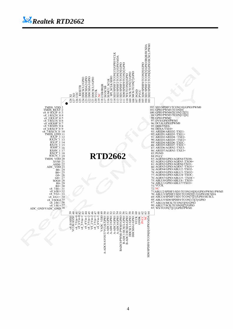
(I/O Legend: A = Analog, I = Input, O = Output, P = Power, G = Ground) Name I/O Pin # Description Note
TMDS_VDD AP 1 TMDS power (3.3 V) TMDS_REXT AI 2 Impedance Match Reference Resistor
For Scan mode,it should be pulled low Scan mode: SI[7:0] is assigned to {124~121,114~111} SO[7:0] is assigned to {110~108,105~101} SE is assigned to 100.
Ref value: 1K ohm
RX2P_0/V8_0 AI 3 TMDS Differential signal Input/VIDEO 8-0
RX2N_0/V8_1 AI 4 TMDS Differential signal Input/VIDEO 8-1
RX1P_0/V8_2 AI 5 TMDS Differential signal Input/VIDEO 8-2
RX1N_0/V8_3 AI 6 TMDS Differential signal Input/VIDEO 8-3
RX0P_0/V8_4 AI 7 TMDS Differential signal Input/VIDEO 8-4
RX0N_0/V8_5 AI 8 TMDS Differential signal Input/VIDEO 8-5
RXCP_0/V8_6 AI 9 TMDS Differential signal Input/VIDEO 8-6
RXCN_0/V8_7 AI 10 TMDS Differential signal Input/VIDEO 8-7
TMDS_GND AG 11 TMDS ground RX2P_1 AI 12 TMDS Differential signal Input RX2N_1 AI 13 TMDS Differential signal Input RX1P_1 AI 14 TMDS Differential signal Input RX1N_1 AI 15 TMDS Differential signal Input RX0P_1 AI 16 TMDS Differential signal Input RX0N_1 AI 17 TMDS Differential signal Input RXCP_1 AI 18 TMDS Differential signal Input RXCN_1 AI 19 TMDS Differential signal Input TMDS_VDD AP 20 TMDS power (3.3 V) AVS0 I 21 ADC vertical sync input no power 5V
tolerance AHS0 I 22 ADC horizontal sync input
AVS0 and AHS0 could be used to select one of three scan chain. AHS0/AVS0: 2’b00: {i_chain[2:0], mcu_chain[1:0], vbi_chain[2:0]} 2’b01: d_chain 2’b10: vdec_chain Other are reserved
no power 5V tolerance
ADC_VDD AG 23 ADC Power (1.8V) B0- AI 24 Negative BLUE analog input (Pb-) B0+ AI 25 Positive BLUE analog input (Pb+) G0- AI 26 Negative GREEN analog input (Y-) G0+ AI 27 Positive GREEN analog input (Y+) SOG0 AI 28 Sync-On-Green R0- AI 29 Negative RED analog input (Pr-) R0+ AI 30 Positive RED analog input (Pr+) B1-/V8_7 AI 31 Negative BLUE analog input
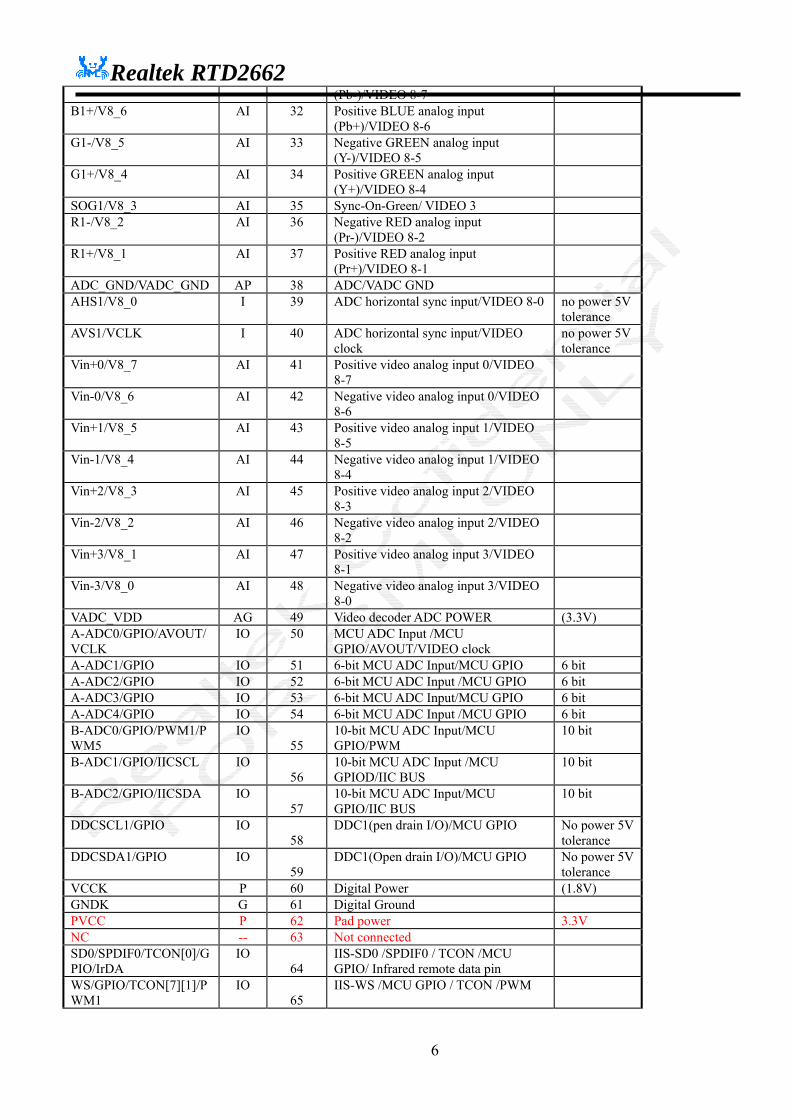
Realtek RTD2662
6
(Pb-)/VIDEO 8-7 B1+/V8_6 AI 32 Positive BLUE analog input
(Pb+)/VIDEO 8-6
G1-/V8_5 AI 33 Negative GREEN analog input (Y-)/VIDEO 8-5
G1+/V8_4 AI 34 Positive GREEN analog input (Y+)/VIDEO 8-4
SOG1/V8_3 AI 35 Sync-On-Green/ VIDEO 3 R1-/V8_2 AI 36 Negative RED analog input
(Pr-)/VIDEO 8-2
R1+/V8_1 AI 37 Positive RED analog input (Pr+)/VIDEO 8-1
ADC_GND/VADC_GND AP 38 ADC/VADC GND AHS1/V8_0 I 39 ADC horizontal sync input/VIDEO 8-0 no power 5V
tolerance AVS1/VCLK I 40 ADC horizontal sync input/VIDEO
clock no power 5V tolerance
Vin+0/V8_7 AI 41 Positive video analog input 0/VIDEO 8-7
Vin-0/V8_6 AI 42 Negative video analog input 0/VIDEO 8-6
Vin+1/V8_5 AI 43 Positive video analog input 1/VIDEO 8-5
Vin-1/V8_4 AI 44 Negative video analog input 1/VIDEO 8-4
Vin+2/V8_3 AI 45 Positive video analog input 2/VIDEO 8-3
Vin-2/V8_2 AI 46 Negative video analog input 2/VIDEO 8-2
Vin+3/V8_1 AI 47 Positive video analog input 3/VIDEO 8-1
Vin-3/V8_0 AI 48 Negative video analog input 3/VIDEO 8-0
VADC_VDD AG 49 Video decoder ADC POWER (3.3V) A-ADC0/GPIO/AVOUT/VCLK
IO 50 MCU ADC Input /MCU GPIO/AVOUT/VIDEO clock
A-ADC1/GPIO IO 51 6-bit MCU ADC Input/MCU GPIO 6 bit A-ADC2/GPIO IO 52 6-bit MCU ADC Input /MCU GPIO 6 bit A-ADC3/GPIO IO 53 6-bit MCU ADC Input/MCU GPIO 6 bit A-ADC4/GPIO IO 54 6-bit MCU ADC Input /MCU GPIO 6 bit B-ADC0/GPIO/PWM1/PWM5
IO 55
10-bit MCU ADC Input/MCU GPIO/PWM
10 bit
B-ADC1/GPIO/IICSCL IO 56
10-bit MCU ADC Input /MCU GPIOD/IIC BUS
10 bit
B-ADC2/GPIO/IICSDA IO 57
10-bit MCU ADC Input/MCU GPIO/IIC BUS
10 bit
DDCSCL1/GPIO IO 58
DDC1(pen drain I/O)/MCU GPIO No power 5V tolerance
DDCSDA1/GPIO IO 59
DDC1(Open drain I/O)/MCU GPIO No power 5V tolerance
VCCK P 60 Digital Power (1.8V) GNDK G 61 Digital Ground PVCC P 62 Pad power 3.3V NC -- 63 Not connected SD0/SPDIF0/TCON[0]/GPIO/IrDA
IO 64
IIS-SD0 /SPDIF0 / TCON /MCU GPIO/ Infrared remote data pin
WS/GPIO/TCON[7][1]/PWM1
IO 65
IIS-WS /MCU GPIO / TCON /PWM
Realtek RTD2662
7
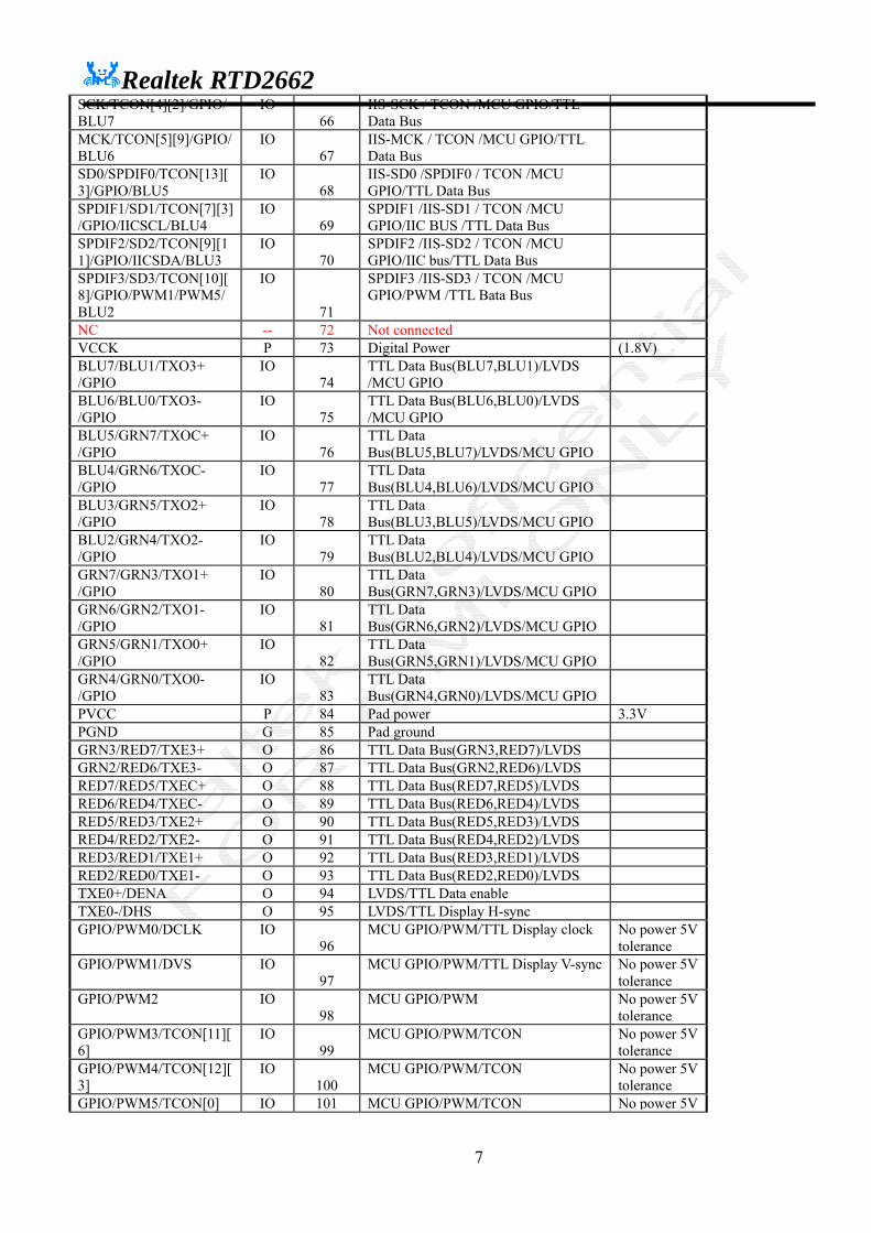
SCK/TCON[4][2]/GPIO/BLU7
IO 66
IIS-SCK / TCON /MCU GPIO/TTL Data Bus
MCK/TCON[5][9]/GPIO/BLU6
IO 67
IIS-MCK / TCON /MCU GPIO/TTL Data Bus
SD0/SPDIF0/TCON[13][3]/GPIO/BLU5
IO 68
IIS-SD0 /SPDIF0 / TCON /MCU GPIO/TTL Data Bus
SPDIF1/SD1/TCON[7][3]/GPIO/IICSCL/BLU4
IO 69
SPDIF1 /IIS-SD1 / TCON /MCU GPIO/IIC BUS /TTL Data Bus
SPDIF2/SD2/TCON[9][11]/GPIO/IICSDA/BLU3
IO 70
SPDIF2 /IIS-SD2 / TCON /MCU GPIO/IIC bus/TTL Data Bus
SPDIF3/SD3/TCON[10][8]/GPIO/PWM1/PWM5/BLU2
IO
71
SPDIF3 /IIS-SD3 / TCON /MCU GPIO/PWM /TTL Bata Bus
NC -- 72 Not connected VCCK P 73 Digital Power (1.8V) BLU7/BLU1/TXO3+ /GPIO
IO 74
TTL Data Bus(BLU7,BLU1)/LVDS /MCU GPIO
BLU6/BLU0/TXO3- /GPIO
IO 75
TTL Data Bus(BLU6,BLU0)/LVDS /MCU GPIO
BLU5/GRN7/TXOC+ /GPIO
IO 76
TTL Data Bus(BLU5,BLU7)/LVDS/MCU GPIO
BLU4/GRN6/TXOC- /GPIO
IO 77
TTL Data Bus(BLU4,BLU6)/LVDS/MCU GPIO
BLU3/GRN5/TXO2+ /GPIO
IO 78
TTL Data Bus(BLU3,BLU5)/LVDS/MCU GPIO
BLU2/GRN4/TXO2- /GPIO
IO 79
TTL Data Bus(BLU2,BLU4)/LVDS/MCU GPIO
GRN7/GRN3/TXO1+ /GPIO
IO 80
TTL Data Bus(GRN7,GRN3)/LVDS/MCU GPIO
GRN6/GRN2/TXO1- /GPIO
IO 81
TTL Data Bus(GRN6,GRN2)/LVDS/MCU GPIO
GRN5/GRN1/TXO0+ /GPIO
IO 82
TTL Data Bus(GRN5,GRN1)/LVDS/MCU GPIO
GRN4/GRN0/TXO0- /GPIO
IO 83
TTL Data Bus(GRN4,GRN0)/LVDS/MCU GPIO
PVCC P 84 Pad power 3.3V PGND G 85 Pad ground GRN3/RED7/TXE3+ O 86 TTL Data Bus(GRN3,RED7)/LVDS GRN2/RED6/TXE3- O 87 TTL Data Bus(GRN2,RED6)/LVDS RED7/RED5/TXEC+ O 88 TTL Data Bus(RED7,RED5)/LVDS RED6/RED4/TXEC- O 89 TTL Data Bus(RED6,RED4)/LVDS RED5/RED3/TXE2+ O 90 TTL Data Bus(RED5,RED3)/LVDS RED4/RED2/TXE2- O 91 TTL Data Bus(RED4,RED2)/LVDS RED3/RED1/TXE1+ O 92 TTL Data Bus(RED3,RED1)/LVDS RED2/RED0/TXE1- O 93 TTL Data Bus(RED2,RED0)/LVDS TXE0+/DENA O 94 LVDS/TTL Data enable TXE0-/DHS O 95 LVDS/TTL Display H-sync GPIO/PWM0/DCLK IO
96 MCU GPIO/PWM/TTL Display clock No power 5V
tolerance GPIO/PWM1/DVS IO
97 MCU GPIO/PWM/TTL Display V-sync No power 5V
tolerance GPIO/PWM2 IO
98 MCU GPIO/PWM No power 5V
tolerance GPIO/PWM3/TCON[11][6]
IO 99
MCU GPIO/PWM/TCON No power 5V tolerance
GPIO/PWM4/TCON[12][3]
IO 100
MCU GPIO/PWM/TCON No power 5V tolerance
GPIO/PWM5/TCON[0] IO 101 MCU GPIO/PWM/TCON No power 5V

Realtek RTD2662
8
tolerance SD3/SPDIF3/TCON[10]/GPIO/PWM0
IO 102
IIS-SD3/SPDIF3/TCON/MCU GPIO/ PWM
No power 5V tolerance
SD2/SPDIF2/TCON[8]/GPIO/IICSCL/PWM1
IO 103
IIS-SD2/SPDIF2/TCON[8]/MCU GPIO/IICSCL/PWM1
No power 5V tolerance
SD1/SPDIF1/TCON[5]/GPIO/IRQB/IICSDA
IO 104
IIS-SD1/SPDIF1/TCON[5]/MCU GPIO/IRQ Bar/IICSDA
No power 5V tolerance
SD0/SPDIF0/TCON[9]/GPIO
IO 105
IIS-SD0/SPDIF0/TCON/MCU GPIO No power 5V tolerance
PVCC P 106 Pad 3.3V power 3.3V PGND P 107 Pad 3.3V GND MCK/TCON[7]/GPIO IO
108 IIS-MCK/TCON/MCU GPIO No power 5V
tolerance SCK/TCON[3]/GPIO IO
109 IIS-SCK/TCON/MCU GPIO No power 5V
tolerance WS/TCON[6]/GPIO IO
110 IIS-WS/TCON/MCU GPIO No power 5V
tolerance SD0/SPDIF0/TCON[4]/GPIO
IO 111
IIS-SD0/SPDIF0/TCON/MCU GPIO No power 5V tolerance
SD1/SPDIF1/TCON[9]/GPIO
IO 112
IIS-SD1/SPDIF1/TCON/MCU GPIO No power 5V tolerance
SD2/SPDIF2/TCON[1]/GPIO/IrDA
IO 113
IIS-SD2/SPDIF2/TCON/MCU GPIO/Infrared remote data pin
No power 5V tolerance
SD3/SPDIF3/TCON[13]/GPIO/VCLK
IO 114
IIS-SD3/SPDIF3/TCON/MCU GPIO/VIDEO 8-clock
No power 5V tolerance
SPI_SCLK/SDIO IO 115
SPI flash serial data input/external MCU serial control I/F data in
No power 5V tolerance
SI/MCU_SCLK IO 116
SPI flash serial clock/external MCU serial control I/F clock
No power 5V tolerance
SO/SCSB IO 117
SPI flash serial data output /external MCU serial control I/F chip select
No power 5V tolerance
CEB/IRQB IO
118
SPI flash chip enable bar/IRQ Bar Note:It should be pulled down to 0 v or pulled up to 3.3 v in order to designate the MCU type(Internal MCU(0 volts) or External MCU(3.3 volts)).
No power 5V tolerance
NC -- 119 Not connected VCCK P 120 Digital 1.8V Power 1.8V DDCSCL3/GPIO IO
121
DDC3(Open drain I/O)/MCU GPIO No power 5V
tolerance DDCSDA3/GPIO IO
122
DDC3(Open drain I/O)/MCU GPIO No power 5V
tolerance DDCSDA2/GPIO IO
123
DDC2(Open drain I/O)/MCU GPIO No power 5V
tolerance DDCSCL2/GPIO IO
124
DDC2(Open drain I/O)/MCUGPIO No power 5V
tolerance RESETB I
125
Chip Reset Bar Low active; No power 5V tolerance
CEC I/O
126
CEC bus Pull up 27k ohm resistance to 3.3V power; No power 5V tolerance

Realtek RTD2662
9
XO AO 127
Crystal Output No power 5V tolerance
XI AI 128
Crystal Input No power 5V tolerance
MCU GPIO assignment PIN No. MCU GPIO Name
50 P6.0
51 P6.1
52 P6.2
53 P6.3
54 P6.4
55 P6.5

Realtek RTD2662
10
56 P6.6
57 P6.7
58 P3.0/RXD(I/O)
59 P3.1/TXD(O)
64 P1.0/T2(I)
65 P1.1/T2EX(I)
66 P1.2/CLKO2(O)
67 P1.3
68 P1.4
69 P1.5
70 P1.6
71 P1.7
74 P9.0
75 P9.1
76 P9.2
77 P9.3
78 P9.4
79 PA.0
80 PA.1
81 PA.2
82 PA.3
83 PA.4
94 P5.0 (removed)
95 P5.1 (removed)
96 P5.2
97 P5.3
98 P5.4
99 P5.5
100 P5.6
101 P5.7
102 P7.6
103 P7.5
104 P7.4
105 P8.0
108 P8.1/CLKO1(O)
109 P3.2/INT0(I)
110 P3.3/INT1(I)
Realtek RTD2662
11
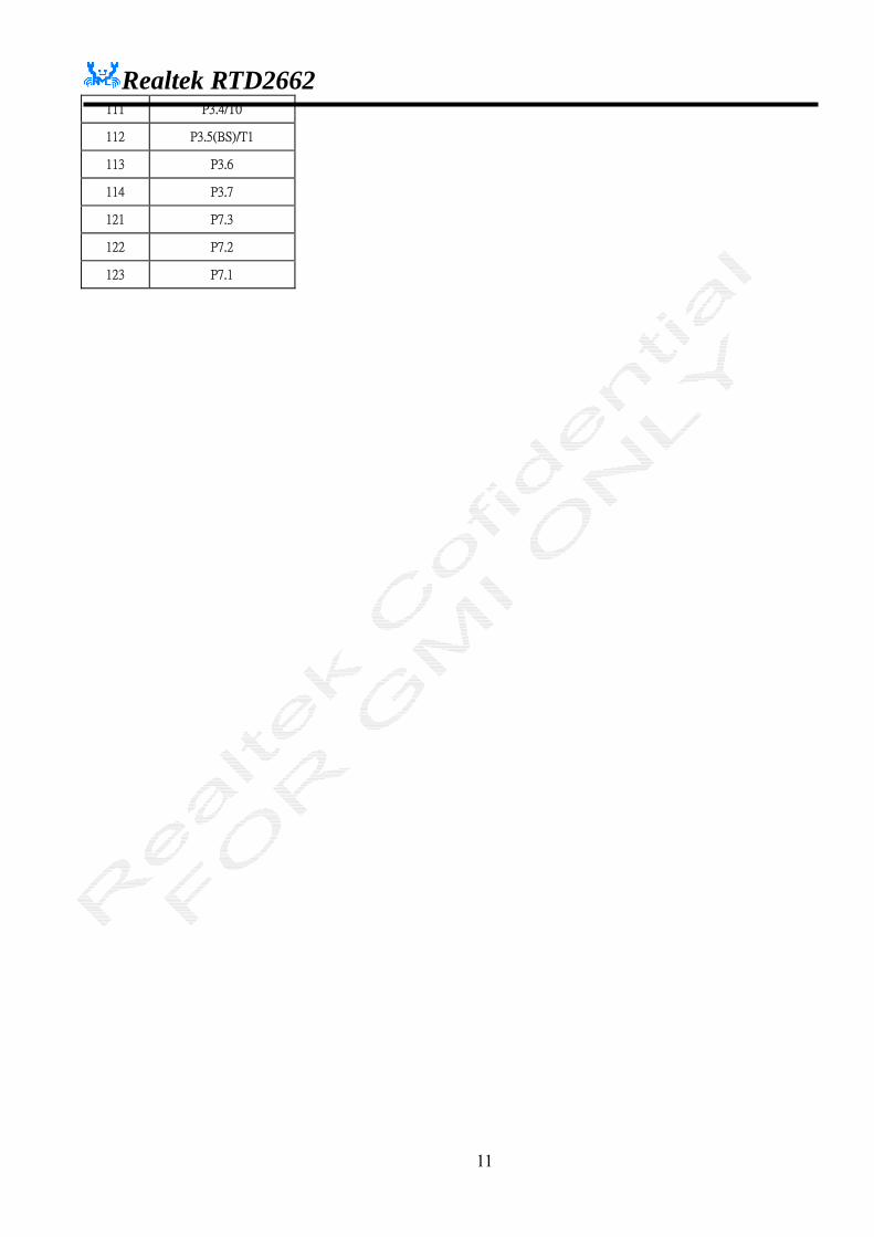
111 P3.4/T0
112 P3.5(BS)/T1
113 P3.6
114 P3.7
121 P7.3
122 P7.2
123 P7.1

Realtek RTD2662
12
2. Chip Data Path Block Diagram
Figure 1

Realtek RTD2662
13
3. Electric Specification DC Characteristics Table 1 Absolute Maximum Ratings
PARAMETER SYMBOL MIN TYP MAX UNITS
Voltage on Input (5V tolerant) VIN -1 5 V
Electrostatic Discharge VESD ±2.5 kV
Latch-Up ILA ±100 mA
Ambient Operating Temperature TA 0 70 ºC
Storage temperature (plastic) TSTG -55 125 ºC
Thermal Resistance (Junction to Air) θJA 25 ºC/W
Junction Acceptable Temperature Tj 125 ºC
Table 2 DC Characteristics/Operating Condition (0℃<TA<70℃)
【Power consumption:Embedded MCU】 Dot-pattern(check_11). 【1】 VGA-in: 1600x1200/75Hz,display to 1680x1050/75Hz,DCLK=170MHz.
Pattern Generator:『Chroma 2227』;Pattern Name:『Dot』pattern 【2】 HDMI-in: 1600x1200/60Hz,display to 1680x1050/60Hz.
Pattern Generator:『QunatumData 882』;Pattern Name:『Check11』(256 gray scale) 【3】 Video Decoder-in:DVD-player;AV-in;display to 1680x1050
Power Name Voltage Operating(mA) Power saving(mA)
Power down(mA)
VCCK(core)(VGA) 1.8V 438 14.9 5.9 VCCK(core)(HDMI) 1.8V 455 8.5 6.1
VCCK(core)(Video Decoder) 1.8V 232 8.6 6.1 ADC_VDD 1.8V 123 0.1 0.1
TMDS_VDD 3.3V 173 19.9 19.9 VADC_VDD 3.3V 65.6 0.1 0.1 PVCC(LVDS) 3.3V 78.5 2.5 2.5 PVCC(TTL) 3.3V 34.1 12.8 12.8

Realtek RTD2662
14
4. Mechanical Specification
128 Pin Package
Realtek RTD2662
15
5. Ordering Information