Room-temperature-deposited dielectrics and...
13
Room-temperature-deposited dielectrics and superconductors for integrated photonics J EFFREY M. S HAINLINE , 1, ⇤ S ONIA M. BUCKLEY, 1 N IMA N ADER , 1 C ALE M. G ENTRY, 2 K EVIN C. C OSSEL , 1 J USTIN W. C LEARY, 3 MILO Š P OPOVI ´ C , 2 N ATHAN R. N EWBURY, 1 S AE WOO N AM, 1 AND R ICHARD P. MIRIN 1 ⇤ je↵[email protected] 1 National Institute of Standards and Technology, 325 Broadway, Boulder, CO, 80305, USA 2 Department of Electrical, Computer and Energy Engineering, University of Colorado, Boulder, CO, 80309, USA 3 Air Force Research Laboratory, Sensors Directorate, 2241 Avionics Circle, Wright Patterson Air Force Base, Ohio 45433, USA Abstract: We present an approach to fabrication and packaging of integrated photonic devices that utilizes waveguide and detector layers deposited at near-ambient temperature. All lithography is performed with a 365 nm i-line stepper, facilitating low cost and high scalability. We have shown low-loss SiN waveguides, high-Q ring resonators, critically coupled ring resonators, 50/50 beam splitters, Mach-Zehnder interferometers (MZIs) and a process-agnostic fiber packaging scheme. We have further explored the utility of this process for applications in nonlinear optics and quantum photonics. We demonstrate spectral tailoring and octave-spanning supercontinuum generation as well as the integration of superconducting nanowire single photon detectors with MZIs and channel-dropping filters. The packaging approach is suitable for operation up to 160 ◦ C as well as below 1 K. The process is well suited for augmentation of existing foundry capabilities or as a stand-alone process. c 2017 Optical Society of America OCIS codes: (130.0130) Integrated optics; (130.3990) Micro-optical devices; (230.3120) Integrated optics devices; (230.4000) Microstructure fabrication; (230.7370) Waveguides; (230.0040) Detectors. References and links 1. F. Kish, D. Welch, R. Nagarajan, J. Pleumeekers, V. Lal, M. Ziari, A. Nilsson, M. Kato, S. Murthy, P. Evans, S. Corzine, M. Mitchell, P. Samra, J. Rahn, M. V. Leeuwen, J. Stewart, D. Lambert, R. Muthiah, H.-S. Tsai, J. Bostak, A. Dentai, K.-T. Wu, H. Sun, D. Pavinski, J. Zhang, J. Tang, J. McNicol, M. Kuntz, V. Dominic, B. Taylor, R. Salvatore, M. Fisher,A. Spannagel, E. Strezelecka, P. Studenkov, M. Raburn, W. Williams, D.Christini, K. T. S. Agashe, R. Malendevich, G. Goldfarb, S. Melle, C. Joyner, M. Kaufman, and S. Grubb, “Current status of large-scale InP photonic integrated circuits,” IEEE J. Sel. Top. Quantum Electron. 17, 1470 (2011). 2. N. Nader and K.C. Cossel and E. Baumann and I.R. Coddington and N.R. Newbury and R. Mirin and J.M. Shainline, “Spectral engineering of frequency combs using deposited waveguides”, in Proceedings of Conference on Lasers and Electro-optics (CLEO, 2016). 3. F. Vollmer and S. Arnold, “Whispering-gallery-mode biosensing: label-free detection down to single molecules,” Nat. Methods 5, 591 (2008). 4. N. Jokerst, M. Royal, S. Palit, L. Luan, S. Dhar, and T. Tyler, “Chip scale integrated microresonator sensing systems,” J. Biophotonics 2, 212 (2009). 5. A. Washburn, L. Gunn, and R. Bailey, “Label-free quantitation of a cancer biomarker in complex media using silicon photonic microring resonators,” Anal. Chem. 81, 9499 (2009). 6. A. Washburn, M. Luchansky, A. Bowman, and R. Bailey, “Quantitative, label-free detection of five protein biomarkers using multiplexed arrays of silicon photonic microring resonators,” Anal. Chem. 82, 69 (2010). 7. Y. Chen, F. Yu, C. Yang, J. Song, L. Tang, M. Li, and J.-J. He, “Label-free biosensing using cascaded double-microring resonators integrated with microfluidic channels,” Opt. Comm. 344, 129 (2015). 8. K. Yamada, T. Tsuchizawa, H. Nishi, R. Kou, T. Hiraki, K. Takeda, H. Fukuda, Y. Ishikawa, K. Wada, and T. Yamamoto, “High-performance silicon photonics technology for telecommunications applications,” Sci. Technol. Adv. Mater. 15, 024603 (2014). 9. C. Doerr, “Silicon photonic integration in telecommunications,” Front. Phys. 3, 37 (2015). Vol. 25, No. 9 | 1 May 2017 | OPTICS EXPRESS 10322 #282457 https://doi.org/10.1364/OE.25.010322 Journal © 2017 Received 7 Dec 2016; revised 14 Apr 2017; accepted 16 Apr 2017; published 26 Apr 2017
Transcript of Room-temperature-deposited dielectrics and...
Room-temperature-deposited dielectrics andsuperconductors for integrated photonicsJEFFREY M. SHAINLINE,1,⇤ SONIA M. BUCKLEY,1 NIMA NADER,1
CALE M. GENTRY,2 KEVIN C. COSSEL,1 JUSTIN W. CLEARY,3 MILOŠPOPOVIC,2 NATHAN R. NEWBURY,1 SAE WOO NAM,1 AND RICHARDP. MIRIN1
⇤ je↵[email protected] Institute of Standards and Technology, 325 Broadway, Boulder, CO, 80305, USA2Department of Electrical, Computer and Energy Engineering, University of Colorado, Boulder, CO,80309, USA3Air Force Research Laboratory, Sensors Directorate, 2241 Avionics Circle, Wright Patterson Air ForceBase, Ohio 45433, USA
Abstract: We present an approach to fabrication and packaging of integrated photonic devicesthat utilizes waveguide and detector layers deposited at near-ambient temperature. All lithographyis performed with a 365 nm i-line stepper, facilitating low cost and high scalability. We haveshown low-loss SiN waveguides, high-Q ring resonators, critically coupled ring resonators, 50/50beam splitters, Mach-Zehnder interferometers (MZIs) and a process-agnostic fiber packagingscheme. We have further explored the utility of this process for applications in nonlinear opticsand quantum photonics. We demonstrate spectral tailoring and octave-spanning supercontinuumgeneration as well as the integration of superconducting nanowire single photon detectors withMZIs and channel-dropping filters. The packaging approach is suitable for operation up to160 �C as well as below 1 K. The process is well suited for augmentation of existing foundrycapabilities or as a stand-alone process.c� 2017 Optical Society of America
OCIS codes: (130.0130) Integrated optics; (130.3990) Micro-optical devices; (230.3120) Integrated optics devices;(230.4000) Microstructure fabrication; (230.7370) Waveguides; (230.0040) Detectors.
References and links1. F. Kish, D. Welch, R. Nagarajan, J. Pleumeekers, V. Lal, M. Ziari, A. Nilsson, M. Kato, S. Murthy, P. Evans,
S. Corzine, M. Mitchell, P. Samra, J. Rahn, M. V. Leeuwen, J. Stewart, D. Lambert, R. Muthiah, H.-S. Tsai,J. Bostak, A. Dentai, K.-T. Wu, H. Sun, D. Pavinski, J. Zhang, J. Tang, J. McNicol, M. Kuntz, V. Dominic, B. Taylor,R. Salvatore, M. Fisher, A. Spannagel, E. Strezelecka, P. Studenkov, M. Raburn, W. Williams, D. Christini, K. T. S.Agashe, R. Malendevich, G. Goldfarb, S. Melle, C. Joyner, M. Kaufman, and S. Grubb, “Current status of large-scaleInP photonic integrated circuits,” IEEE J. Sel. Top. Quantum Electron. 17, 1470 (2011).
2. N. Nader and K.C. Cossel and E. Baumann and I.R. Coddington and N.R. Newbury and R. Mirin and J.M. Shainline,“Spectral engineering of frequency combs using deposited waveguides”, in Proceedings of Conference on Lasers andElectro-optics (CLEO, 2016).
3. F. Vollmer and S. Arnold, “Whispering-gallery-mode biosensing: label-free detection down to single molecules,”Nat. Methods 5, 591 (2008).
4. N. Jokerst, M. Royal, S. Palit, L. Luan, S. Dhar, and T. Tyler, “Chip scale integrated microresonator sensing systems,”J. Biophotonics 2, 212 (2009).
5. A. Washburn, L. Gunn, and R. Bailey, “Label-free quantitation of a cancer biomarker in complex media using siliconphotonic microring resonators,” Anal. Chem. 81, 9499 (2009).
6. A. Washburn, M. Luchansky, A. Bowman, and R. Bailey, “Quantitative, label-free detection of five protein biomarkersusing multiplexed arrays of silicon photonic microring resonators,” Anal. Chem. 82, 69 (2010).
7. Y. Chen, F. Yu, C. Yang, J. Song, L. Tang, M. Li, and J.-J. He, “Label-free biosensing using cascaded double-microringresonators integrated with microfluidic channels,” Opt. Comm. 344, 129 (2015).
8. K. Yamada, T. Tsuchizawa, H. Nishi, R. Kou, T. Hiraki, K. Takeda, H. Fukuda, Y. Ishikawa, K. Wada, andT. Yamamoto, “High-performance silicon photonics technology for telecommunications applications,” Sci. Technol.Adv. Mater. 15, 024603 (2014).
9. C. Doerr, “Silicon photonic integration in telecommunications,” Front. Phys. 3, 37 (2015).
Vol. 25, No. 9 | 1 May 2017 | OPTICS EXPRESS 10322
#282457 https://doi.org/10.1364/OE.25.010322 Journal © 2017 Received 7 Dec 2016; revised 14 Apr 2017; accepted 16 Apr 2017; published 26 Apr 2017

10. C. Kachris and I. Tomkos, “A survey on optical interconnects for data centers,” IEEE Commun. Surveys Tutorials 14,1021 (2012).
11. D. Nikolova, S. Rumley, D. Calhoun, A. Li, R. Hendry, P. Samadi, and K. Bergman, “Scaling silicon photonic switchfabrics for data center interconnection networks,” Opt. Express 23, 1159 (2015).
12. S. Rumley, D. Nikolova, R. Hendry, Q. Li, D. Calhoun, and K. Bergman, “Silicon photonics for exascale systems,” J.Lightwave Technol. 33, 547 (2015).
13. C. Sun, M. Wade, Y. Lee, J. Orcutt, L. Alloatti, M. Georgas, A. Waterman, J. Shainline, R. Avizienis, S. Lin, B. Moss,R. Kumar, F. Pavanello, A. Atabaki, H. Cook, A. Ou, J. Leu, Y.-H. Chen, K. Asanovic, R. Ram, M. Popovic, andV. Stojanovic, “Single-chip microprocessor that communicates directly using light,” Nature 528, 534 (2015).
14. D. Thomson, A. Zilkie, J. E. Bowers, T. Komljenovic, G. T. Reed, L. Vivien, D. Marris-Morini, E. Cassan, L. Virot,and J. -M Fédéli, “Roadmap on silicon photonics”, J. Opt. 18, 073003 (2016).
15. A. E.-J. Lim, J. Song, Q. Fang, C. Li, X. Tu, N. Duan, K. K. Chen, R. P.-C. Tern, and T.-Y. Liow, “Review of siliconphotonics foundry e↵orts”, IEEE J. Sel. Top. Quantum Electron. 20, 8300112 (2014).
16. K. A. Williams, E. A. J. M Bente, D. Heiss, Y. Jiao, K. Lawniczuk, X. J. M. Leijtens, J. J. G. M van der Tol, andM. K. Smit, “InP photonic circuits using generic integration”, Photon. Res. 3, B60 (2015).
17. “American Institute for Manufacturing Integrated Photonics,” URL http://www.aimphotonics.com/.18. K. Wörho↵, R. G. Heideman, A. Leinse and M. Hoekman, “TriPleX: a versatile dielectric photonic platform”, Adv.
Opt. Technol. 4, 189 (2015).19. D. J. Moss, R. Morandotti, A. L. Gaeta, and M. Lipson, “New CMOS-compatible platforms based on silicon nitride
and Hydex for nonlinear optics,” Nat. Photonics 7, 597–607 (2013).20. R. A. Soref, S. J. Emelett, and W. R. Buchwald, “Silicon waveguided components for the long-wave infrared region,”
J. Opt. A 8, 840–848 (2006).21. J. M. Shainline, S. M. Buckley, R. P. Mirin, and S. W. Nam, “Superconducting optoelectronic circuits for neuromor-
phic computing,” Phys. Rev. Appl. 7, 034013 (2017).22. F. Marsili, V. B. Verma, J. A. Stern, S. Harrington, A. E. Lita, T. Gerrits, I. Vayshenker, B. Baek, M. D. Shaw, R. P.
Mirin, and S. W. Nam, “Detecting single infrared photons with 93% system e�ciency,” Nat. Photonics 7, 210–214(2013).
23. Y. H. D. Lee and M. Lipson, “Back-End Deposited Silicon Photonics for Monolithic Integration on CMOS,” IEEE J.Sel. Top. Quantum Electron. 19, 8200207 (2013).
24. Z. Shao, Y. Chen, H. Chen, Y. Zhang, F. Zhang, J. Jian, Z. Fan, L. Liu, C. Yang, L. Zhou, and S. Yu, “Ultra-lowtemperature silicon nitride photonic integration platform,” Opt. Express 24, 1865 (2016).
25. S. Zhu, G. Lo, and D. Kwong, “Low-loss amorphous silicon wire waveguide for integrated photonics: e↵ect offabrication process and the thermal stability,” Opt. Express 18, 25283 (2010).
26. R. Takei, S. Manako, E. Omoda, Y. Sakakibara, M. Mori, and T. Kamei, “Sub-1 dB/cm submicrometer-scaleamorphous silicon waveguide for backend on-chip optical interconnect,” Opt. Express 22, 4779 (2014).
27. W. Sacher, Z. Yong, J. Mikkelsen, A. Bois, Y. Yang, J. Mak, P. Dumais, D. Goodwill, C. Ma, J. Jeong, E. Bernier, andJ. Poon, “Multilayer silicon nitride-on-silicon integrated photonic platform for 3D photonic circuits,” in Proceedingsof Conference on Lasers and Electro-optics (CLEO, 2016) p. JTh4C.3.
28. A. Biberman, K. Preston, G. Hendry, N. Sherwood-Droz, J. Chan, J. S. Levy, M. Lipson, and K. Bergman, “Photonicnetwork-on-chip architectures using multilayer deposited silicon materials for high-performance chip multiproces-sors,” ACM J. Emerg. Technol. Comput. Syst. 7, 1–25 (2011).
29. N. Sherwood-Droz and M. Lipson, “Scalable 3D dense integration of photonics on bulk silicon,” Opt. Express 19,17758 (2011).
30. J. F. Bauters, M. J. R. Heck, D. John, D. Dai, M.-C. Tien, J. S. Barton, A. Leinse, R. G. Heideman, D. J. Blumenthal,and J. E. Bowers, “Ultra-low-loss high-aspect-ratio Si3N4 waveguides,” Opt. Express 19, 3163 (2011).
31. C. R. Doerr, L. Chen, Y.-K. Chen, and L. L. Buhl, “Wide bandwidth silicon nitride grating coupler,” IEEE Photon.Technol. Lett. 22, 1461–1463 (2010).
32. H. Zhang, C. Li, X. Tu, H. Zhou, X. Luo, M. Yu, and P. G.-Q. Lo, “High e�ciency silicon nitride grating couplerwith DBR,” in Optical Fiber Communication Conference (OSA, 2014), p. Th1A.4.
33. G. Roelkens, D. Van Thourhout, and R. Baets, “High e�ciency Silicon-on-Insulator grating coupler based on apoly-Silicon overlay,” Opt. Express 14, 11622 (2006).
34. G. Maire, L. Vivien, G. Sattler, A. Kazmierczak, B. Sanchez, K. B. Gylfason, A. Griol, D. Marris-Morini, E. Cassan,D. Giannone, H. Sohlström, and D. Hill, “High e�ciency silicon nitride surface grating couplers,” Opt. Express 16,328 (2008).
35. A. Mekis, S. Gloeckner, G. Masini, A. Narasimha, T. Pinguet, S. Sahni, and P. De Dobbelaere, “A Grating-Coupler-Enabled CMOS Photonics Platform,” IEEE J. Sel. Top. Quantum Electron. 17, 597–608 (2011).
36. W. S. Zaoui, A. Kunze, W. Vogel, M. Berroth, J. Butschke, F. Letzkus, and J. Burghartz, “Bridging the gap betweenoptical fibers and silicon photonic integrated circuits,” Opt. Express 22, 1277 (2014).
37. J. Notaros and M. Popovic, “Band-structure approach to synthesis of grating couplers with ultra-high couplinge�ciency and directivity,” in Optical Fiber Communication Conference (OSA, 2015), p. Th3F.2.
38. J. F. Bauters, M. L. Davenport, M. J. R. Heck, J. K. Doylend, A. Chen, A. W. Fang, and J. E. Bowers, “Silicon onultra-low-loss waveguide photonic integration platform,” Opt. Express 21, 544 (2013).
39. M. Pfei↵er, A. Kordts, V. Brasch, M. Zervas, M. Geiselmann, J. Jost, and T. Kippenberg, “Photonic damascene
Vol. 25, No. 9 | 1 May 2017 | OPTICS EXPRESS 10323

process for integrated high-Q microresonator based nonlinear photonics,” Optica 3, 20 (2016).40. Y. Xuan, Y. Liu, L. Varghese, A. Metcalf, X. Xue, P.-H. Wang, K. Han, J. Jaramillo-Villegas, A. Noman, C. Wang,
S. Kim, M. Teng, Y. Lee, B. Niu, L. Fan, J. Wang, D. Leaird, A. Weiner, and M. Qi, “High-Q silicon nitridemicroresonators exhibiting low-power frequency comb initiation,” Optica 3, 1171 (2016).
41. J. K. S. Poon, W. D. Sacher, Y. Huang, and G.-Q. Lo, “Multilayer silicon nitride-on-silicon integrated photonicplatforms,” in 2015 IEEE Compound Semiconductor Integrated Circuit Symposium (IEEE, 2015), pp. 1–4.
42. W. H. P. Pernice, C. Schuck, O. Minaeva, M. Li, G. N. Goltsman, A. V. Sergienko, and H. X. Tang, “High-speed andhigh-e�ciency travelling wave single-photon detectors embedded in nanophotonic circuits,” Nat. Commun. 3, 1325(2012).
43. C. Schuck, X. Guo, L. Fan, X. Ma, M. Poot, and H. X. Tang, “Quantum interference in heterogeneous superconducting-photonic circuits on a silicon chip,” Nat. Commun. 7, 10352 (2016).
44. J. P. Sprengers, A. Gaggero, D. Sahin, S. Jahanmirinejad, G. Frucci, F. Mattioli, R. Leoni, J. Beetz, M. Lermer,M. Kamp, S. HoÌLfling, R. Sanjines, and A. Fiore, “Waveguide superconducting single-photon detectors for integratedquantum photonic circuits,” Appl. Phys. Lett. 99, 181110 (2011).
45. F. Najafi, J. Mower, N. C. Harris, F. Bellei, A. Dane, C. Lee, X. Hu, P. Kharel, F. Marsili, S. Assefa, K. K. Berggren,and D. Englund, “On-chip detection of non-classical light by scalable integration of single-photon detectors,” Nat.Commun. 6, 5873 (2015).
46. M. K. Akhlaghi, E. Schelew, and J. F. Young, “Waveguide integrated superconducting single-photon detectorsimplemented as near-perfect absorbers of coherent radiation,” Nat. Commun. 6, 8233 (2015).
47. K. Srinivasan and O. Painter, “Optical fiber taper coupling and high-resolution wavelength tuning of microdiskresonators at cryogenic temperatures,” Appl. Phys. Lett. 90, 031114 (2007).
48. J. D. Cohen, S. M. Meenehan, and O. Painter, “Optical coupling to nanoscale optomechanical cavities for nearquantum-limited motion transduction,” Opt. Express 21, 11227 (2013).
49. A. Beyer, R. Briggs, F. Marsili, J. D. Cohen, S. M. Meenehan, O. J. Painter, and M. Shaw, “Waveguide-coupledsuperconducting nanowire single-photon detectors,” in Conference on Lasers and Electro-optics (OSA, 2015), p.STh1I.2.
50. T. Barwicz and Y. Taira, “Low-cost interfacing of fibers to nanophotonic waveguides: design for fabrication andassembly tolerances,” IEEE Photon. J. 6, 1–18 (2014).
51. A. S. Mayer, A. Klenner, A. R. Johnson, K. Luke, M. R. E. Lamont, Y. Okawachi, M. Lipson, A. L. Gaeta, andU. Keller, “Frequency comb o↵set detection using supercontinuum generation is silicon nitride waveguides,” Opt.Express 12, 015440 (2015).
52. J. M. C. Boggio, D. Bodenmüller, T. Fremberg, R. Haynes, M. M. Roth, R. Eisermann, M. Lisker, L. Zimmermann,and M. Böhm, “Dispersion engineered silicon nitride waveguides by geometrical and refractive-index optimization,”J. Opt. Soc. Am. B 31, 2846 (2014).
53. Y. Okawachi, K. Saha, J. S. Levy, Y. H. Wen, M. Lipson, and A. L. Gaeta, “Octave-spanning frequency combgeneration in a silicon nitride chip,” Opt. Lett. 36, 3398 (2011).
54. I. Coddington, N. Newbury, and W. Swann, “Dual-comb spectroscopy,” Optica 3, 414 (2016).55. S. Diddams, D. Jones, J. Ye, S. Cundi↵, J. Hall, J. Ranka, R. Windeler, R. Holzwarth, T. Udem, and T. Hänsch,
“Direct link between microwave and optical frequencies with a 300 THz femtosecond laser comb,” Phys. Rev. Lett.84, 5102 (2000).
56. J. Hall, “Defining and measuring optical frequencies,” Rev. Mod. Phys. 78, 1279 (2006).57. A. Bartels, D. Heinecke, and S. Diddams, “10-GHz self-referenced optical frequency comb,” Science 326, 681
(2009).58. S. Diddams, “The evolving optical frequency comb,” J. Opt. Soc. Am. B 27, B51 (2010).59. J. Orcutt, S. Tang, S. Kramer, K. Mehta, H. Li, , V. Stojanovic, and R. Ram, “Low-loss polysilicon waveguides
fabricated in an emulated high-volume electronics process,” Opt. Express 20, 7243 (2012).60. L. Sinclair, J.-D. Deschênes, L. Sonderhouse, W. C. Swann, I. H. Khader, E. Baumann, N. R. Newbury, and
I. Coddington, “A compact optically coherent fiber frequency comb,” Rev. Sci. Instrum. 86, 081301 (2015).61. Q. Lin, O. J. Painter, and G. P. Agrawal, “Nonlinear optical phenomena in silicon waveguides,” Opt. Express 15,
16604 (2007).62. R. K. W. Lau, M. R. E. Lamont, A. G. Gri�th, Y. Okawachi, M. Lipson, and A. L. Gaeta, “Octave-spanning
mid-infrared supercontinuum generation in silicon nanowaveguides,” Opt. Lett. 39, 4518 (2014).63. B. Kuyken, T. Ideguchi, S. Holzner, M. Yan, T. W. Hänsch, J. van Campenhout, P. Verheyen, S. Coen, F. Leo,
R. Baets, G. Roelkens, and N. Picqué, “An octave-spanning mid-infrared frequency comb generated in a siliconnanophotonic wire waveguide,” Nat. Commun. 6, 6310 (2015).
64. P. Cavalier, J.-C. VilleÌAgier, P. Feautrier, C. Constancias, and A. Morand, “Light interference detection on-chip byintegrated SNSPD counters,” AIP Adv. 1, 042120 (2011).
65. M. G. Tanner, L. S. E. Alvarez, W. Jiang, R. J. Warburton, Z. H. Barber, and R. H. Hadfield, “A superconductingnanowire single photon detector on lithium niobate,” Nanotechnology 23, 505201 (2012).
66. H. A. Atikian, A. Eftekharian, A. Jafari Salim, M. J. Burek, J. T. Choy, A. Hamed Majedi, and M. Loncar,“Superconducting nanowire single photon detector on diamond,” Appl. Phys. Lett. 104, 122602 (2014).
67. O. Kahl, S. Ferrari, V. Kovalyuk, G. N. Goltsman, A. Korneev, and W. H. P. Pernice, “Waveguide integratedsuperconducting single-photon detectors with high internal quantum e�ciency at telecom wavelengths,” Sci. Rep. 5,
Vol. 25, No. 9 | 1 May 2017 | OPTICS EXPRESS 10324

10941 (2015).68. D. Sahin, A. Gaggero, J.-W. Weber, I. Agafonov, M. A. Verheijen, F. Mattioli, J. Beetz, M. Kamp, S. Hofling,
M. C. M. van de Sanden, R. Leoni, and A. Fiore, “Waveguide nanowire superconducting single-photon detectorsfabricated on GaAs and the study of their optical properties,” IEEE J. Sel. Top. Quantum Electron. 21, 1–10 (2015).
69. G. Gol’tsman, O. Okunev, G. Chulova, A. Lipatov, A. Semenov, K. Smirnov, B. Voronov, A. Dzardanov, C. Williams,and R. Sobolewski, “Picosecond superconducting single-photon optical detector,” Appl. Phys. Lett. 79, 705 (2001).
70. C. Natarajan, M. Tanner, and R. Hadfield, “Superconducting nanowire single-photon detectors: physics and applica-tions,” Supercond. Sci. Tech. 25, 063001 (2012).
71. D. Liu, L. You, S. Chen, X. Yang, Z. Wang, Y. Wang, X. Xie, and M. Jiang, “Electrical characteristics of supercon-ducting nanowire single photon detector,” IEEE Trans. Appl. Supercond. 23, 2200804 (2013).
72. A. Kerman, J. Yang, R. Molnar, E. Dauler, and K. Berggren, “Electrothermal feedback in superconducting nanowiresingle-photon detectors,” Phys. Rev. B 79, 100509 (2009).
73. S. Jahanmirinejad and A. Fiore, “Proposal for a superconducting photon number resolving detector with largedynamic range,” Opt. Express 20, 5017 (2012).
74. A. Casaburi, R. Heath, M. Ejrnaes, C. Nappi, R. Cristiano, and R. Hadfield, “Experimental evidence for photoinducedvortex crossing in current carrying superconducting strips,” Phys. Rev. B 92, 214512 (2015).
75. A. Casaburi, R. Heath, M. Tanner, R. Cristiano, M. Ejrnaes, C. Nappi, and R. Hadfield, “Current distribution in aparallel configuration superconducting strip-line detector,” Appl. Phys. Lett. 103, 013503 (2013).
76. F. Marsili, D. Bitauld, A. Gaggero, S. Jahanmirinejad, R. Leoni, F. Mattioli, and A. Fiore, “Physics and application ofphoton number resolving detectors based on superconducting parallel nanowires,” New J. Phys. 11, 045022 (2009).
77. A. Divochiy, F. Marsili, D. Bitauld, A. Gaggero, R. Leoni, F. Mattioli, A. Korneev, V. Seleznev, N. Kaurova,O. Minaeva, G. Gol’tsman, K. Lagoudakis, M. Benkhaoul, F. Lévy, and A. Fiore, “Superconducting nanowirephoton-number-resolving detector at telecommunication wavelengths,” Nat. Photon. 2, 302 (2008).
78. J. Yang, A. Kerman, E. Dauler, V. Anant, K. Rosfjord, and K. Berggren, “Modeling the electrical and thermalresponse of superconducting nanowire single-photon detectors,” IEEE Trans. Appl. Supercond. 17, 581 (2007).
79. M. Fitch, B. Jacobs, T. Pittman, and J. Franson, “Photon-number resolution using time-multiplexed single-photondetectors,” Phys. Rev. A 68, 043814 (2003).
80. G. N. Gol’tsman, O. Okunev, G. Chulkova, A. Lipatov, A. Semenov, K. Smirnov, B. Voronov, A. Dzardanov,C. Williams, and R. Sobolewski, “Picosecond superconducting single-photon optical detector,” Appl. Phys. Lett. 79,705 (2001).
81. B. Baek, A. E. Lita, V. Verma, and S. W. Nam, “Superconducting a-Wx
Si1�x
nanowire single-photon detector withsaturated internal quantum e�ciency from visible to 1850 nm,” Appl. Phys. Lett. 98, 251105 (2011).
1. Introduction
The first on-chip photonic components were developed in the mid-1980s, and the subsequentthree decades have demonstrated exponential growth in the data capacity per die [1] due tothe miniaturization enabled by integrated photonic devices. Photonic integrated circuits arenow playing a role in advanced technologies with applications ranging from atmospheric spec-troscopy [2] and medical diagnostics [3–7] to telecommunications [8, 9], data centers, [10, 11]and supercomputers [12, 13]. Each of these integrated photonic application spaces opens newpossibilites for science and technology.
The chip-scale photonic devices enabling this innovation are manufactured using lithographictechniques developed by the semiconductor industry, and it is the precision, accuracy, andreliability of these fabrication techniques that has enabled the rapid adoption of integratedphotonics for myriad applications. However, the broad range of integrated photonic technologiesand application spaces makes it more di�cult to create a technology roadmap [14] and a foundryprocess [15–17] with broad applicability than it has been for electronics.
Nevertheless, many e↵orts currently exist which serve a variety of integrated photonicsapplications including silicon photonics [14, 15, 17] and InP photonics [16]. Yet for nonlinearand quantum optics, other dielectric material platforms are more desirable [18]. For nonlinearoptics in the visible and near-infrared, Si is not a desirable waveguiding medium due to highone- and two-photon absorption [19]. For nonlinear optics in the mid-IR, the absorption of astandard buried SiO2 layer is problematic [20]. For superconducting optoelectronic networks [21]and quantum-optical applications, high detection e�ciency is required, and superconductingdetectors are a very desirable option [22]. Such detectors are not likely to be incorporated into afoundry process in the near term.
Vol. 25, No. 9 | 1 May 2017 | OPTICS EXPRESS 10325
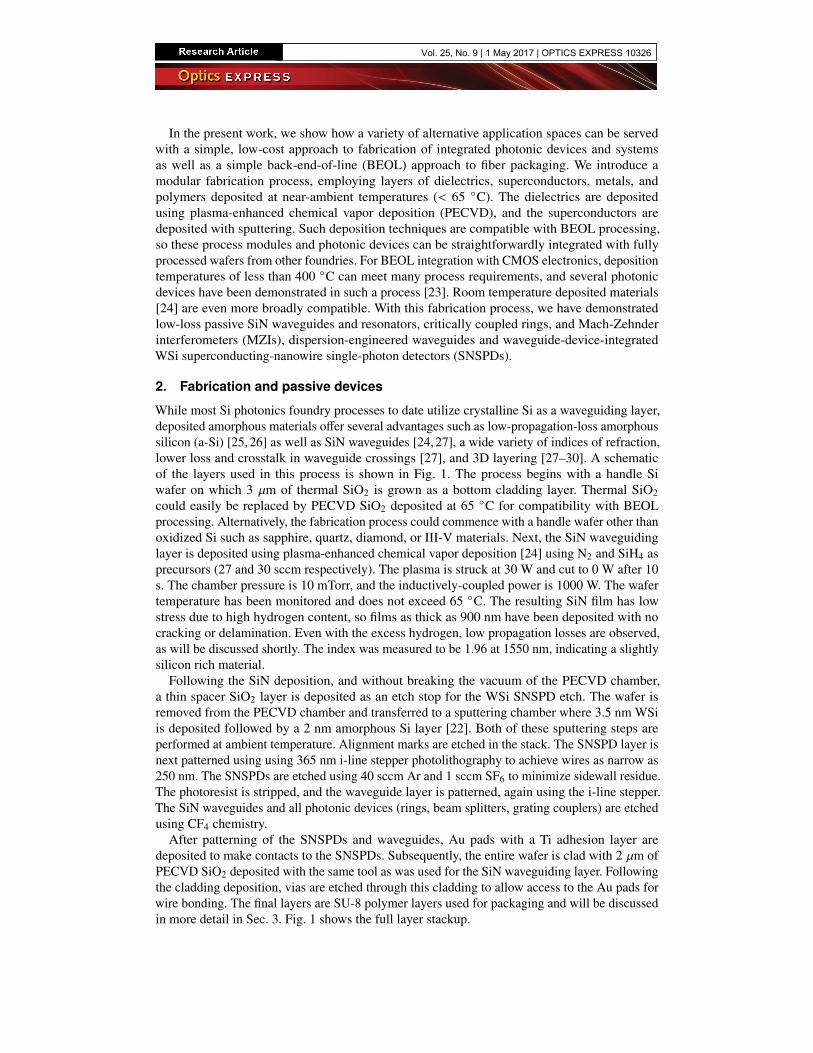
In the present work, we show how a variety of alternative application spaces can be servedwith a simple, low-cost approach to fabrication of integrated photonic devices and systemsas well as a simple back-end-of-line (BEOL) approach to fiber packaging. We introduce amodular fabrication process, employing layers of dielectrics, superconductors, metals, andpolymers deposited at near-ambient temperatures (< 65 �C). The dielectrics are depositedusing plasma-enhanced chemical vapor deposition (PECVD), and the superconductors aredeposited with sputtering. Such deposition techniques are compatible with BEOL processing,so these process modules and photonic devices can be straightforwardly integrated with fullyprocessed wafers from other foundries. For BEOL integration with CMOS electronics, depositiontemperatures of less than 400 �C can meet many process requirements, and several photonicdevices have been demonstrated in such a process [23]. Room temperature deposited materials[24] are even more broadly compatible. With this fabrication process, we have demonstratedlow-loss passive SiN waveguides and resonators, critically coupled rings, and Mach-Zehnderinterferometers (MZIs), dispersion-engineered waveguides and waveguide-device-integratedWSi superconducting-nanowire single-photon detectors (SNSPDs).
2. Fabrication and passive devices
While most Si photonics foundry processes to date utilize crystalline Si as a waveguiding layer,deposited amorphous materials o↵er several advantages such as low-propagation-loss amorphoussilicon (a-Si) [25, 26] as well as SiN waveguides [24, 27], a wide variety of indices of refraction,lower loss and crosstalk in waveguide crossings [27], and 3D layering [27–30]. A schematicof the layers used in this process is shown in Fig. 1. The process begins with a handle Siwafer on which 3 µm of thermal SiO2 is grown as a bottom cladding layer. Thermal SiO2could easily be replaced by PECVD SiO2 deposited at 65 �C for compatibility with BEOLprocessing. Alternatively, the fabrication process could commence with a handle wafer other thanoxidized Si such as sapphire, quartz, diamond, or III-V materials. Next, the SiN waveguidinglayer is deposited using plasma-enhanced chemical vapor deposition [24] using N2 and SiH4 asprecursors (27 and 30 sccm respectively). The plasma is struck at 30 W and cut to 0 W after 10s. The chamber pressure is 10 mTorr, and the inductively-coupled power is 1000 W. The wafertemperature has been monitored and does not exceed 65 �C. The resulting SiN film has lowstress due to high hydrogen content, so films as thick as 900 nm have been deposited with nocracking or delamination. Even with the excess hydrogen, low propagation losses are observed,as will be discussed shortly. The index was measured to be 1.96 at 1550 nm, indicating a slightlysilicon rich material.
Following the SiN deposition, and without breaking the vacuum of the PECVD chamber,a thin spacer SiO2 layer is deposited as an etch stop for the WSi SNSPD etch. The wafer isremoved from the PECVD chamber and transferred to a sputtering chamber where 3.5 nm WSiis deposited followed by a 2 nm amorphous Si layer [22]. Both of these sputtering steps areperformed at ambient temperature. Alignment marks are etched in the stack. The SNSPD layer isnext patterned using using 365 nm i-line stepper photolithography to achieve wires as narrow as250 nm. The SNSPDs are etched using 40 sccm Ar and 1 sccm SF6 to minimize sidewall residue.The photoresist is stripped, and the waveguide layer is patterned, again using the i-line stepper.The SiN waveguides and all photonic devices (rings, beam splitters, grating couplers) are etchedusing CF4 chemistry.
After patterning of the SNSPDs and waveguides, Au pads with a Ti adhesion layer aredeposited to make contacts to the SNSPDs. Subsequently, the entire wafer is clad with 2 µm ofPECVD SiO2 deposited with the same tool as was used for the SiN waveguiding layer. Followingthe cladding deposition, vias are etched through this cladding to allow access to the Au pads forwire bonding. The final layers are SU-8 polymer layers used for packaging and will be discussedin more detail in Sec. 3. Fig. 1 shows the full layer stackup.
Vol. 25, No. 9 | 1 May 2017 | OPTICS EXPRESS 10326
Optical ber
SU-8 pedestal
SU-8 ber collar SU-8 ber collar
PECVD SiO2 (cladding)WSi (superconductor)PECVD SiN (waveguide)
thermal SiO2 (cladding)
Si wafer (handle) 500 1000 1500 2000 2500 30001.952.002.052.102.152.202.25
Inde
x of
Ref
ract
ion
ex o
f Ref
ract
ion
Wavelength [nm]
Fig. 1. A schematic of the layers used in this fabrication process. The inset shows the indexof refraction of the SiN waveguide layer as measured with spectroscopic ellipsometry.
1550 1560 1570 1580 1590 1600 1610 1620
-26-24-22-20-18-16-14-12
Inse
rtion
Los
s [dB
]
Wavelength [nm] 1573.8 1573.85 1573.9 1573.950
0.2
0.4
0.6
0.8
1
Wavelength [nm]
Tran
smiss
ion
[a.u
.] DataFit
Q = 125,000
1546 1547 1548 1549 1550 1551 1552 1553 1554-25-20-15-10-50
Inse
rtion
Los
s [dB
]
Wavelength [nm]1545 1550 1555 1560 1565 1570 1575
-30-25-20-15-10-50
Inse
rtion
Los
s [dB
]
Wavelength [nm]
In1 Out1In1 Out2In2 Out1In2 Out2
5µm10µm
200µm120µm
(g)
(h)
(c)
(d)
(b)
(a) (e)
(f)
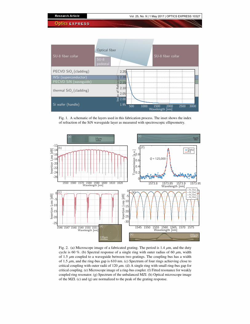
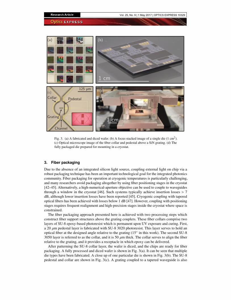
Fig. 2. (a) Microscope image of a fabricated grating. The period is 1.4 µm, and the dutycycle is 60 %. (b) Spectral response of a single ring with outer radius of 60 µm, widthof 1.5 µm coupled to a waveguide between two gratings. The coupling bus has a widthof 1.5 µm, and the ring-bus gap is 610 nm. (c) Spectrum of four rings achieving close tocritical coupling with outer radii of 120 µm. (d) A single ring with small ring-bus gap forcritical coupling. (e) Microscope image of a ring-bus coupler. (f) Fitted resonance for weaklycoupled ring resonator. (g) Spectrum of the unbalanced MZI. (h) Optical microscope imageof the MZI. (c) and (g) are normalized to the peak of the grating response.
Vol. 25, No. 9 | 1 May 2017 | OPTICS EXPRESS 10327
To illustrate the utility of this process, we demonstrate several photonic devices. Figures2(a) and (b) show microscope images of a SiN grating and the spectral response of a singlering coupled to a waveguide between two gratings. The insertion loss due to the gratings is 6.8dB/coupler, in close agreement with the finite-di↵erence time-domain simulated value of 6.68dB/coupler. The 3 dB bandwidth of these couplers is 90 nm, and the 3 dB angular tolerance is3�. The low index contrast of the SiN/SiO2 grating results in a structure which is insensitiveto position in the longitudinal direction. In the transverse direction, the alignment tolerance isdominated by the Gaussian mode profile of the fiber mode, and it drops to 1/e2 (13.5%) ofmaximum value with a distance corresponding to the mode field diameter of 10.4 µm. This givesa lateral 3 dB alignment tolerance of 6.1 µm. The spectrum in Fig. 2(b) was taken after thefibers were fixed in place as described in Sec. 3. While the lower index contrast of SiN limitsgrating e�ciency, the insertion loss can be significantly improved with a thicker SiN layer [31],a backside mirror [32], a second deposited layer [33], or an additional (partial) etch step [34].With a backside mirror (which could be integrated easily in this process), insertion loss of 2.6dB has been demonstrated [32], and insertion loss of < 2 dB has been simulated [31] in a SiNsingle-etch process similar to this work. The addition of more and higher index layers, such asa-Si, could also improve grating coupler insertion loss. State-of-the-art Si grating couplers haveachieved insertion losses of less than 1 dB [35, 36], while grating couplers in a two-layer CMOSprocess with ⇠ 0.2 dB coupling loss have recently been designed [37]. All of these approachesare compatible with the deposited photonics process and packaging approach presented here.
Next we investigated critically coupled ring resonators. In Fig. 2(c) we show the transmissionspectrum of four rings coupled to a single bus. One such ring is shown in Fig. 2(d). Each of thefour rings has a di↵erent gap ranging from 360 nm to 500 nm on the mask, corresponding to 610nm to 750 nm after fabrication. The optimally coupled device achieved > 25 dB extinction acrossseveral FSRs. To assess parasitic losses in the critically coupled rings, the most critically coupledresonance from each FSR of the spectrum in Fig. 2(c) was fit to a Lorentzian to obtain a Q factor.The mean Q of these resonances was 43,250 (corresponding to an intrinsic Q of 86,500), and thestandard deviation was 2,630.
In addition to critically coupled ring resonators, we have investigated weakly coupled, high-Qrings. Figure 2(e) shows a microscope image of a ring-bus coupler, and Fig. 2(f) shows a fit to aweakly coupled resonance with Q-factor of 125,000, corresponding to 2.5 dB/cm propagationloss. The five resonances of this ring closest to 1570 nm were fit to obtain Qs. The mean Q ofthe data set was 110,000 (corresponding to 2.8 dB/cm), and the standard deviation was 8,900.Sidewall roughness due to patterning with i-line lithography is likely the leading contribution tolinear propagation losses, as lower losses have been observed in waveguides of similar materialwhen patterned with electron beam lithography (0.8 dB/cm) [24] as well as within this processwhen resist reflow was employed (1.8 dB/cm), as discussed in Sec. 4. This is comparable toPECVD nitride deposited at 400�C [23], but significantly higher than high temperature depositedLPCVD SiN, where losses of less than 0.1 dB/cm have been observed [30, 38–40]. Siliconwaveguides typically exhibit propagation losses near 3 dB/cm [41]. Finally, in Fig. 2(g) we showthe spectrum of an unbalanced MZI [Fig. 2(h)] demonstrating > 25 dB extinction between allports across > 40 nm of spectral bandwidth. This extinction demonstrates that the adiabatic beamsplitters created in our process are nearly ideal with no more than 1.5% deviation from 50/50splitting. If scattered light, noise from the laser source, or unbalanced losses are a↵ecting thevisibility, then the beam splitters are even closer to 50/50.
The thermal tuning of passive integrated-photonic devices is often advantageous. A processlayer for heaters can be straightforwardly inserted either with evaporated metals or PECVD-deposited and doped a-Si. The a-Si option is particularly attractive due to the decreased electro-migration relative to metals, and addition of a-Si to the process is also likely to lead to detectorsfor high-peak-power pulses used for nonlinear optics.
Vol. 25, No. 9 | 1 May 2017 | OPTICS EXPRESS 10328
(a)
(c) (d)
(b)
PedestalCollar
Channel
Grating
125 µm
1 cm
1 cm
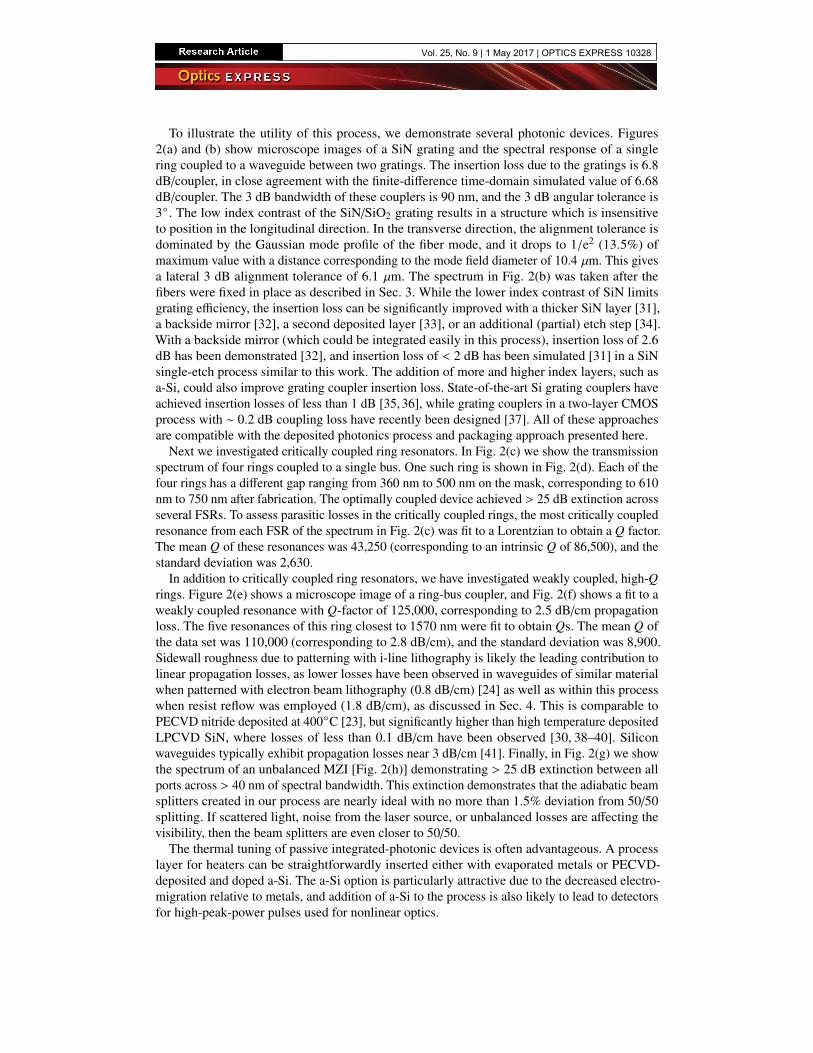
Fig. 3. (a) A fabricated and diced wafer. (b) A focus-stacked image of a single die (1 cm2).(c) Optical microscope image of the fiber collar and pedestal above a SiN grating. (d) Thefully packaged die prepared for mounting in a cryostat.
3. Fiber packaging
Due to the absence of an integrated silicon light source, coupling external light on chip via arobust packaging technique has been an important technological goal for the integrated photonicscommunity. Fiber packaging for operation at cryogenic temperatures is particularly challenging,and many researchers avoid packaging altogether by using fiber positioning stages in the cryostat[42–45]. Alternatively, a high-numerical-aperture objective can be used to couple to waveguidesthrough a window in the cryostat [46]. Such systems typically achieve insertion losses > 7dB, although lower insertion losses have been reported [45]. Cryogenic coupling with taperedoptical fibers has been achieved with losses below 1 dB [47]. However, coupling with positioningstages requires frequent realignment and high-precision stages inside the cryostat where space isconstrained.
The fiber packaging approach presented here is achieved with two processing steps whichconstruct fiber support structures above the grating couplers. These fiber collars comprise twolayers of SU-8 epoxy-based photoresist which is permanent upon UV exposure and curing. First,a 20 µm pedestal layer is fabricated with SU-8 3020 photoresist. This layer serves to hold anoptical fiber at the designed angle relative to the grating (15� in this work). The second SU-83050 layer is referred to as the collar, and it is 50 µm thick. The collar serves to align the fiberrelative to the grating, and it provides a receptacle in which epoxy can be delivered.
After patterning the SU-8 collar layer, the wafer is diced, and the chips are ready for fiberpackaging. A fully processed and diced wafer is shown in Fig. 3(a). It can be seen that multipledie types have been fabricated. A close up of one particular die is shown in Fig. 3(b). The SU-8pedestal and collar are shown in Fig. 3(c). A grating coupled to a tapered waveguide is also
Vol. 25, No. 9 | 1 May 2017 | OPTICS EXPRESS 10329
visible, and the inset shows two such fiber collars with a ring coupled to a bus between. In Fig.3(c) one can see that the fiber collar has two channels on the sides of the fiber. The low viscosityof the epoxy enables it to run through these channels into the ellipse housing the fiber. Uponfilling the entire volume, the epoxy is UV-cured. After placing all fibers, an additional amountof epoxy can be delivered to further strengthen the assembly. When packaging is complete, theassembly is mechanically robust and can be handled easily without drift in coupling. A fullypackaged chip suitable for cryogenic applications is shown in Fig. 3(d).
This packaging approach is suitable for a wide range of operating temperatures. With DymaxOP-4-20632 cryogenic epoxy, we demonstrated cooling of a packaged sample down to < 1 K,incurring an additional 1.5 dB insertion loss per coupler. This sample has been thermally cycledtwice with the same performance. Additional thermal cycles have not been attempted. WithNorland Optical Adhesive, we demonstrated heating up to 160 �C. Upon heating to 120 �C anadditional 1 dB insertion loss per coupler was incurred. The sample was held at 120 �C for 16hours with no additional insertion loss. It was then raised to 160 �C incurring an additional 1 dBinsertion loss per coupler. Such packaged chips have been observed to maintain stable couplingfor weeks, and the fully encased fibers are protected from the environment to enable exceptionallongevity.
We wish to use our waveguide devices to perform spectroscopy in outdoor environments, andalso for quantum optical experiments with superconductors in cryogenic environments. Towardthese ends, the packaging approach presented here has several strengths. The simplicity renders ituseful in many contexts, as it does not depend on KOH wet etch steps to form v-grooves [48,49],which can be di�cult from a process-integration standpoint, and it is not dependent on a two-chipassembly [50]. Alignment of the collar relative to the grating is achieved lithographically, so littleoptimization is required. Fiber couplers can be placed anywhere on the die for higher density,not just the periphery, as in many v-groove [48,49] and two-chip approaches [50]. Packaging canbe highly automated as the placement of a fiber in a collar and the epoxy delivery is well-suitedto robotics with machine vision.
4. Applications in nonlinear optics
SiN waveguides provide an excellent platform for nonlinear optics due to their high nonlinearindex (10x larger than silica) [51] and low absorption from visible to infrared wavelengths.Recent progress [52, 53] has revealed opportunities to use group-velocity-dispersion (GVD)engineered devices in conjunction with high-power ultrafast lasers to generate spectra suitablefor applications such as spectroscopy [54], time and frequency metrology [55–58], and noveloptical sources.
Finite-di↵erence frequency domain calculations show near-zero GVD is achieved for wave-lengths in the near-IR by engineering SiN waveguides with thicknesses above 600 nm. For thepresent study, we investigated waveguides with 700 nm thickness. The GVD curves for thesewaveguides are shown in Fig. 4(a) for various waveguide widths. These calculations assumethermal SiO2 as an undercladding, air as an overcladding, and employ the SiN index data shownin Fig. 1(b). Waveguides with widths > 1.4 µm have very flat, near-zero anomalous GVD withone zero crossing at short wavelengths. These waveguides can be used for octave-spanning super-continuum generation which is useful for self-referenced frequency combs [55, 56, 58]. Slightlynarrower waveguides have anomalous GVD with two zero crossings. As the waveguide width isreduced below 1 µm, the anomalous GVD region becomes narrower and drops more steeply tonegative values. These waveguides generate narrow, flat-top spectra. Such spectra improve thesignal-to-noise ratio for spectroscopic applications targeting a specific narrow frequency band.
Figure 4(b) and (c) show scanning electron micrographs of fabricated waveguides. In additionto the processing described in Sec. 2, these waveguides incurred a resist reflow at 150 �C forfive minutes before etching. The WSi, SU-8, and overcladding layers were omitted for these
Vol. 25, No. 9 | 1 May 2017 | OPTICS EXPRESS 10330

20µm
1µm0.9 1.1 1.3 1.5 1.7 1.9 2.1 2.3-200
-100
0
100
200
300
GVD
[ps/
(nm
·km
)]
Wavelength [µm]
width = 900nmwidth = 1.1µmwidth = 1.4µmwidth = 1.7µm
(a)(b)
(c)
Fig. 4. (a) GVD curves for 700 nm thick SiN waveguides with air over-cladding for di↵erentwaveguide widths. (b) Scanning electron micrograph of paperclip waveguide structures formeasuring propagation losses. (c) Tapered waveguide for edge-coupling.
devices. Figure 4(b) shows a waveguide in a paperclip configuration [59] to measure propagationlosses. These measurements give 1.8 dB/cm propagation loss, an improvement over the loss-ringmeasurement of the thin waveguides presented in Sec. 2 (2.5 dB/cm). The loss has not beenobserved to depend on intensity, indicating that multiphoton absorption is a smaller contributionthan sidewall scattering even for femtosecond pulses with 6 kW peak power. Figure 4(c) showsa waveguide with a tapered tip for edge coupling, which was used for these nonlinear opticsexperiments. Insertion loss of 5.2 dB/facet was measured. For spectroscopy applications in thefield or metrology applications in a system, the fiber packaging approach presented in Sec. 3 canbe utilized.
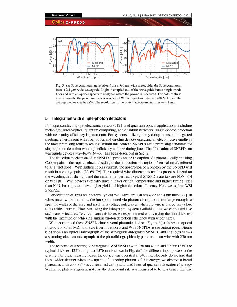
For investigation of nonlinear spectral broadening, a high-power, femtosecond 1550 nm fiberfrequency comb with up to 17 kW peak power and 60 fs pulse duration was used as the lasersource [60]. The source was TE-polarized and coupled into the waveguide tapers with a lensedfiber. Output spectra were recorded as a function of incident power with an optical spectrumanalyzer. The measured outputs of 960 nm- and 2100 nm-wide waveguides are presented inFigs. 5(a) and (b), respectively. Also shown on these plots are the theoretical predictions usingthe GVD curves of Fig. 4(a) in the nonlinear Schrödinger equation (NLSE) [61, 62]. The 960nm device generates a supercontinuum that stays within 20 dB over the wavelength range from1350 nm to 1850 nm and sharply drops beyond this spectral range. This relatively flat spectrumis suitable for spectroscopy wherein a flat spectrum provides a correspondingly flat responsefunction with a uniform signal-to-noise ratio.
In contrast to the spectrum of Fig. 5(a) the spectrum of Fig. 5(b) shows broad supercontinuumgeneration from a 2100 nm-wide waveguide. This supercontinuum covers the spectrum from1050 to 2200 nm when pumped with comb peak power of 5.25 kW. Because sources of phasenoise, such as free-carrier absorption and multiphoton absorption are minimal in SiN, we expectthe supercontinuum process to maintain coherence. Coherence after supercontinuum broadeninghas been demonstrated in Ref. [63]. Such a coherent comb spectrum is suitable for self-referencedfrequency combs. Additionally, due to the design of the GVD zero crossings at 1.1 µm and2.2 µm, the optical power is concentrated at these wavelengths which will be utilized in thedi↵erence-frequency generation process.
These examples of spectral tailoring for spectroscopic applications as well as frequencymetrology applications show the utility of this deposited-waveguide fabrication process fornonlinear optics.
Vol. 25, No. 9 | 1 May 2017 | OPTICS EXPRESS 10331
1.0 1.2 1.4 1.6 1.8 2.0 2.2-60
-50
-40
-30
-20
Wavelength [µm]
Powe
r [dB
m]
NLSEMeasured
1.3 1.4 1.5 1.6 1.7 1.8 1.9-65
-55
-45
-35
-25
-15
Wavelength [µm]
Powe
r [dB
m]
NLSEMeasured
(a) (b)
Fig. 5. (a) Supercontinuum generation from a 960 nm wide waveguide. (b) Supercontinuumfrom a 2.1 µm wide waveguide. Light is coupled out of the waveguide into a single-modefiber and into an optical spectrum analyzer where the power is measured. For both of thesemeasurements, the peak laser power was 5.25 kW, the repetition rate was 200 MHz, and theaverage power was 63 mW. The resolution of the optical spectrum analyzer was 2 nm.
5. Integration with single-photon detectors
For superconducting optoelectronic networks [21] and quantum optical applications includingmetrology, linear-optical quantum computing, and quantum networks, single-photon detectionwith near-unity e�ciency is paramount. For systems utilizing many components, an integratedphotonic environment with fiber optics and on-chip devices operating at telecom wavelengths isthe most promising route to scaling. Within this context, SNSPDs are a promising candidate forsingle-photon detection with high e�ciency and low timing jitter. The fabrication of SNSPDs onwaveguide devices [42–46, 49, 64–68] has been described in Sec. 2.
The detection mechanism of an SNSPD depends on the absorption of a photon locally breakingCooper pairs in the superconductor, leading to the production of a region of normal metal, referredto as a “hot spot”. With su�cient bias current, the absorption of a photon by the SNSPD willresult in a voltage pulse [22, 69–79]. The required wire dimensions for this process depend onthe wavelength of the light and the material properties. Typical SNSPD materials are NbN [80]or WSi [81]. WSi devices typically have a lower critical temperature and higher timing jitterthan NbN, but at present have higher yield and higher detection e�ciency. Here we explore WSiSNSPDs.
For detection of 1550 nm photons, typical WSi wires are 130 nm wide and 4 nm thick [22]. Inwires much wider than this, the hot spot created via photon absorption is not large enough tospan the width of the wire and result in a voltage pulse, even when the wire is biased very closeto its critical current. However, using the lithographic system available to us, we cannot achievesuch narrow features. To circumvent this issue, we experimented with varying the film thicknesswith the intention of achieving similar photon detection e�ciency with wider wires.
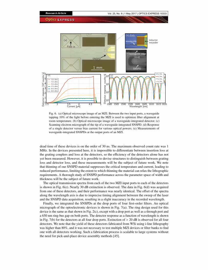
We incorporated these SNSPDs into several photonic devices. Figure 6(a) shows an opticalmicrograph of an MZI with two fiber input ports and WSi SNSPDs at the output ports. Figure6(b) shows an optical micrograph of the waveguide-integrated SNSPD, and Fig. 6(c) showsa scanning electron micrograph of the photolithographically patterned nanowire with 250 nmwidth.
The response of a waveguide-integrated WSi SNSPD with 250 nm width and 3.5 nm (85% thetypical thickness [22]) to light at 1570 nm is shown in Fig. 6(d) for di↵erent input powers at thegrating. For these measurements, the device was operated at 740 mK. Not only do we find thatthese wider, thinner wires are capable of detecting photons of this energy, we observe a broadplateau as a function of bias current, indicating saturated internal quantum detection e�ciency.Within the plateau region near 4 µA, the dark count rate was measured to be less than 1 Hz. The
Vol. 25, No. 9 | 1 May 2017 | OPTICS EXPRESS 10332
50 µm
250nm
inductor meanderwaveguide
waveguide edge
SNSPD
SNSPD
Fiber in
1 mm
1580 1585 1590 1595 1600 1605 1610 1615 1620101
102
103
104
Wavelength [nm]
In1 Out1
In1 Out2
In2 Out1
In2 Out2
Dete
ctor
resp
onse
coun
ts/s
]2.5 3 3.5 4 4.5 50
1
2
3
4
5
6
Current [µA]Dete
ctor
resp
onse
[105
coun
ts/s
]
-70.0 dBm-72.5 dBm-75.0 dBm-77.5 dBm-80.0 dBm-90.0 dBm
(a)
(b)
(c)
(e)(d)
Fig. 6. (a) Optical microscope image of an MZI. Between the two input ports, a waveguidetapping 10% of the light before entering the MZI is used to optimize fiber alignment atroom temperature. (b) Optical microscope image of a waveguide-integrated detector. (c)Scanning electron micrograph of the tip of a waveguide-integrated SNSPD. (d) Responseof a single detector versus bias current for various optical powers. (e) Measurements ofwaveguide-integrated SNSPDs at the output ports of an MZI.
dead time of these devices is on the order of 30 ns. The maximum observed count rate was 1MHz. In the devices presented here, it is impossible to di↵erentiate between insertion loss atthe grating couplers and loss at the detectors, so the e�ciency of the detectors alone has notyet been measured. However, it is possible to devise structures to distinguish between gratingloss and detector loss, and these measurements will be the subject of future work. We notethat thinning of our SNSPD material suppresses the critical temperature and current, leading toreduced performance, limiting the extent to which thinning the material can relax the lithographicrequirements. A thorough study of SNSPD performance across the parameter space of width andthickness will be the subject of future work.
The optical transmission spectra from each of the two MZI input ports to each of the detectorsis shown in Fig. 6(e). Nearly 30 dB extinction is observed. The data in Fig. 6(d) was acquiredfrom one of these detectors, and their performance was nearly identical. The o↵set of the spectraalong the wavelength axis is due to imprecise timing alignment between the sweep of the laserand the SNSPD data acquisition, resulting in a slight inaccuracy in the recorded wavelength.
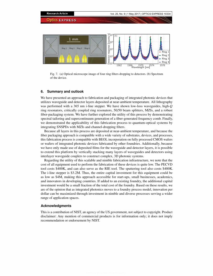
Finally, we integrated the SNSPDs at the drop ports of four first-order filters. An opticalmicrograph of the optoelectronic devices is shown in Fig. 7(a). The ring design used for thisdevice is the same as that shown in Fig. 2(c), except with a drop port as well as a through port anda 650 nm ring-bus gap on both ports. The detector response as a function of wavelength is shownin Fig. 7(b) for the detectors at all four drop ports. Extinction of > 20 dB is observed for all fourdetectors. We note that the yield of these detectors fabricated from WSi using i-line lithographywas higher than 80%, and it was not necessary to test multiple MZI devices or filter banks to findone with all detectors working. Such a fabrication process is scalable to large systems withoutthe need for pick-and-place device assembly methods [45].
Vol. 25, No. 9 | 1 May 2017 | OPTICS EXPRESS 10333
Ring 1 Ring 2 Ring 3 Ring 4
1562 1566 1570 1574 1578101
102
103
104
105
Wavelength [nm]
Dete
ctor
resp
onse
[cou
nts/
s]
Ring 1Ring 2Ring 3Ring 4
(a)(b)
1 mm
Fig. 7. (a) Optical microscope image of four ring filters dropping to detectors. (b) Spectrumof the device.
6. Summary and outlook
We have presented an approach to fabrication and packaging of integrated photonic devices thatutilizes waveguide and detector layers deposited at near-ambient temperature. All lithographywas performed with a 365 nm i-line stepper. We have shown low-loss waveguides, high-Qring resonators, critically coupled ring resonators, 50/50 beam splitters, MZIs, and a robustfiber-packaging system. We have further explored the utility of this process by demonstratingspectral tailoring and supercontinuum generation of a fiber-generated frequency comb. Finally,we demonstrated the applicability of this fabrication process to quantum-optical systems byintegrating SNSPDs with MZIs and channel-dropping filters.
Because all layers in this process are deposited at near-ambient temperature, and because thefiber packaging approach is compatible with a wide variety of substrates, devices, and processes,this fabrication process is compatible with BEOL incorporation on fully processed CMOS wafersor wafers of integrated photonic devices fabricated by other foundries. Additionally, becausewe have only made use of deposited films for the waveguide and detector layers, it is possibleto extend this platform by vertically stacking many layers of waveguides and detectors usinginterlayer waveguide couplers to construct complex, 3D photonic systems.
Regarding the utility of this scalable and nimble fabrication infrastructure, we note that thecost of all equipment used to perform the fabrication of these devices is quite low. The PECVDtool costs $400K, and can also serve as the RIE tool. The sputtering tool also costs $400K.The i-line stepper is $3.2M. Thus, the entire capital investment for this equipment could beas low as $4M, making this approach accessible for start-ups, small businesses, academics,and innovators in developing countries. If added to an existing foundry, the additional capitalinvestment would be a small fraction of the total cost of the foundry. Based on these results, weare of the opinion that as integrated photonics moves to a foundry process model, innovation perdollar can be maximized through investment in nimble and diverse processes serving a widerrange of application spaces.
Acknowledgments
This is a contribution of NIST, an agency of the US government, not subject to copyright. Productdisclaimer: Any mention of commercial products is for information only; it does not implyrecommendation or endorsement by NIST.
Vol. 25, No. 9 | 1 May 2017 | OPTICS EXPRESS 10334