Roll-to-roll Manufacturing in Electronics: Making it work! · Roll-to-roll Manufacturing in...
18
IEEE Components, Packaging and Manufacturing Technology Chapter, Santa Clara Valley Section Presented January 10, 2017 www.cpmt.org/scv 1 Roll-to-roll Manufacturing in Electronics: Making it work! IEEE CPMT lunch meeting Texas Instruments Conference Center, Santa Clara January 10, 2017 Peter Salmon, Presenter Outline Perspectives A glimpse of the future Things we already know The proposed technology 2 The proposed technology Technology comparisons & wrap-up
Transcript of Roll-to-roll Manufacturing in Electronics: Making it work! · Roll-to-roll Manufacturing in...

IEEE Components, Packaging and Manufacturing Technology Chapter, Santa Clara Valley Section
Presented January 10, 2017
www.cpmt.org/scv 1
Roll-to-roll Manufacturing in Electronics: Making it work!
IEEE CPMT lunch meetinggTexas Instruments Conference Center, Santa ClaraJanuary 10, 2017Peter Salmon, Presenter
Outline
Perspectives
A glimpse of the future
Things we already know
The proposed technology
2
The proposed technology
Technology comparisons & wrap-up

IEEE Components, Packaging and Manufacturing Technology Chapter, Santa Clara Valley Section
Presented January 10, 2017
www.cpmt.org/scv 2
Perspectives
The rotary press is a kind of Roll-to-roll (R2R) machine that’s been around a long time
Gravure printing wherein an image is engraved on a rotating drum was first used to print Gravure printing, wherein an image is engraved on a rotating drum, was first used to print bank notes in 1772 in Germany
R2R is fundamentally different from batch processing – it is a continuous process that can lead to agile manufacturing and increased automation. It could provide10X reduction in cost. Accordingly, it has been pursued by multiple parties and technological disciplines
Although passive RFID tags have been a spectacular success (at around 12 cents each),not many complex circuits are produced today in volume
3
not many complex circuits are produced today in volume
Current state-of-the-art for R2R is a production ink-jet system costing ~ $500,000, or a gravure press costing around $1,000,000 (and requiring cylinders costing around $5,000 each)
A glimpse of the future
4Complex PCB
R2RComplex Electronic System

IEEE Components, Packaging and Manufacturing Technology Chapter, Santa Clara Valley Section
Presented January 10, 2017
www.cpmt.org/scv 3
Seven things we already know
5
1. Electrophotography
In a Xerographic printer a static latent image can be developedg p p g pusing dry toner to produce images with good resolution
The surface potential on the photoconductor typically varies by 70-90V
A typical toner particle is 10 µm in diameter, has a charge-to-massratio of 12 µC/gm, electrical charge of 8fC (50,000 electrons)*
5 µm polymerized toners have been produced in volume
6
* Provides a benchmark for the proposed process

IEEE Components, Packaging and Manufacturing Technology Chapter, Santa Clara Valley Section
Presented January 10, 2017
www.cpmt.org/scv 4
II. Ion Implantation
Ion implantation machines can be adapted to embed positive and negative charges in a substratei i busing scanning beams
Electron and proton beams can penetrate several millimeters through air
Such beams may provide a good way to prepare target substrates with embedded alignment patterns and index marks, ahead of a production run
In some systems the beams may be used to program the pattern of a layer to be depositedsee U S Pat 9 227 220 issued Jan 2016- see U.S. Pat. 9,227,220 issued Jan. 2016
7
III. Through Silicon Vias (TSVs)
Make electrical connections on wafer back side, so as not to interfere with image formation
8
, g Provide precision alignment between features on front and back side of wafer
IEEE Components, Packaging and Manufacturing Technology Chapter, Santa Clara Valley Section
Presented January 10, 2017
www.cpmt.org/scv 5
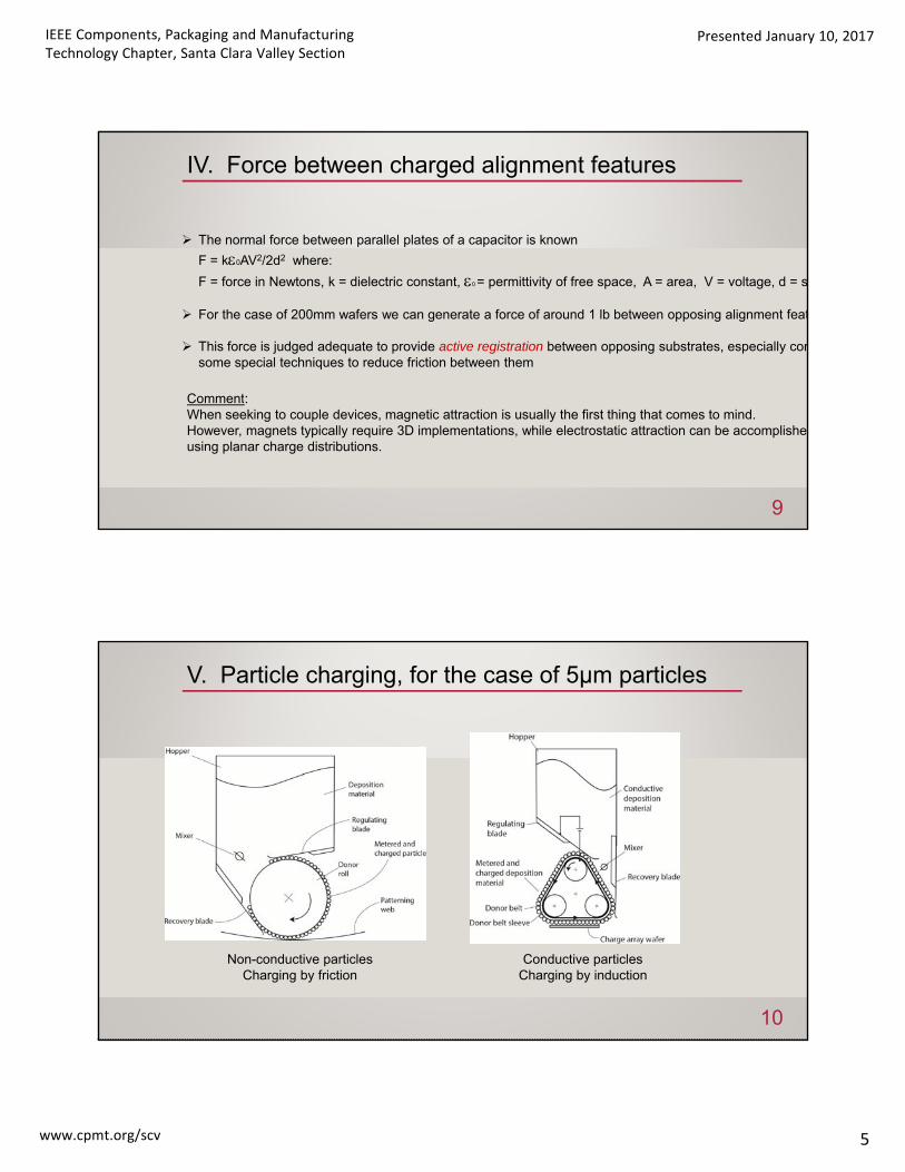
IV. Force between charged alignment features
The normal force between parallel plates of a capacitor is known
F = k0AV2/2d2 where:F k0AV /2d where:
F = force in Newtons, k = dielectric constant, 0 = permittivity of free space, A = area, V = voltage, d = s
For the case of 200mm wafers we can generate a force of around 1 lb between opposing alignment feat
This force is judged adequate to provide active registration between opposing substrates, especially consome special techniques to reduce friction between them
Comment:
9
Comment:When seeking to couple devices, magnetic attraction is usually the first thing that comes to mind.However, magnets typically require 3D implementations, while electrostatic attraction can be accomplishedusing planar charge distributions.
V. Particle charging, for the case of 5µm particles
Non-conductive particlesCharging by friction
Conductive particlesCharging by induction
10

IEEE Components, Packaging and Manufacturing Technology Chapter, Santa Clara Valley Section
Presented January 10, 2017
www.cpmt.org/scv 6
VI. Encapsulated Particles (like encapsulated printer toners)
Encapsulated particles have been produced using apolymerizing process to create spherical particlespolymerizing process to create spherical particles
The shell material can potentially be tribo-active for charging,and removable after deposition using a finishing process
Standardized encapsulated particles can produce similarsize and charging characteristics across a wide range ofdeposition materials
Spherical particles act like ball bearings, producing alubricating effect in the proposed system
11
VII. Alignment via surface tension of solder
Claimed alignment tolerance ~ 1µm
12
As a point of comparison, a modern gravure printer has an Overlay Printing Registration Accuracy, OPRA, of around 40 µm in the printing direction and 16 µm in the perpendicular direction

IEEE Components, Packaging and Manufacturing Technology Chapter, Santa Clara Valley Section
Presented January 10, 2017
www.cpmt.org/scv 7
The Proposed Technology
13
Charge Array Wafer
The wafer is used in the R2R manufacturing system- it is not diced into separate chips
Note:W th it ith i h
14
We can program the capacitors with varying chargevalues, according to the pattern to be created. This iwhat leads to an agile manufacturing system, notrequiring any traditional masks

IEEE Components, Packaging and Manufacturing Technology Chapter, Santa Clara Valley Section
Presented January 10, 2017
www.cpmt.org/scv 8
Fault tolerance
To achieve good yield at the wafer level, as opposed to the normal case comprising relatively small-sized chips, a fault tolerant architecture and redundant circuit elements can be usedbe used.
A cell size for capacitor plates may be set at a small dimension, say 8 µm, while the size of the smallest circuit feature is set larger, say 24 µm. Then a single point failure of an 8x8 µm cell within a 9-cell feature, 24x24 µm, should be acceptable, after fusing a deposited layer for example.
We can also provide redundant address decoders, and switch from the primary A-decoder to the backup B-decoder whenever we have difficulty addressing a cell.
15
to the backup B decoder whenever we have difficulty addressing a cell.
System logic and memory will be provided using special-purpose chips on the back side of the wafer, including microprocessor, RAM, flash memory, and programmable voltage sources. If any of these chips prove to be defective, they can be replaced.
8µm capacitor cell, with 5µm deposition particle
By comparison, a human hair hasa diameter of around 80 µm.
16

IEEE Components, Packaging and Manufacturing Technology Chapter, Santa Clara Valley Section
Presented January 10, 2017
www.cpmt.org/scv 9
3D model of deposited spheres – idealized view - 5µm cells
Col
RowBlack representspositively charged cells
Negatively chargeddeposition particles
Fused stripes ofdeposition materialon target substrate
Result after transfer & fusing
17
White represents negatively charged cells
deposition particles on target substrate
In practice, deposition particles are somewhat irregular
18

IEEE Components, Packaging and Manufacturing Technology Chapter, Santa Clara Valley Section
Presented January 10, 2017
www.cpmt.org/scv 10
Range of deposition particles: Macro, Micro, and Nano
5 di t 5
5µm standardized spheres as macro particles Charge control agents, CCAs, and flow control agents, FCAs, are probably required with these
larger particles
5nm ≤ diameter ≤ 5µm
- a huge range
larger particles Method is adaptable to macro, micro, and nano-scale particles Micro and nano-scales include:
- gas ions and polar molecules for atomic or molecular layer deposition- charged or polar nano-particulates
Particles may be delivered in gas, liquid, or powder form
19
Simulation of imaging potential
Wafersurface
20

IEEE Components, Packaging and Manufacturing Technology Chapter, Santa Clara Valley Section
Presented January 10, 2017
www.cpmt.org/scv 11
Alignment: “Active Registration”
Chevronalignment
Approximate overall alignment using mechanical transport system Precision local alignment using embedded charge patterns; target substrate is loosely draped Lowered friction using spherical particles and modulated decoupling force Restoring alignment force is proportional to local misalignment Alignment method is effective while opposing substrates are either stationary or moving
alignmentfeatures
21
Deposition Stations: Phase 1: Imaging of Macro Particles
NoteThe source material can also be delivered as anairborne powder, a liquid, or polar gas molecules,or ionized gas (plasma)
22

IEEE Components, Packaging and Manufacturing Technology Chapter, Santa Clara Valley Section
Presented January 10, 2017
www.cpmt.org/scv 12
Deposition Station: Phase II: Transfer & Fusing
23
Deposition Station: Phase III: Finishing
The target substrate is accessible for providing additional processing steps
Physical processing may include rolling, for smoothing or compressing a deposited layer
Heat processing, for curing or annealing
Radiation processing, e.g. UV for curing a deposited layer
24
Laser processing, to vaporize a binding material, or melt particles to form a continuous solid
Coating of a conforming layer, which may be selectively reactive with an underlying layer

IEEE Components, Packaging and Manufacturing Technology Chapter, Santa Clara Valley Section
Presented January 10, 2017
www.cpmt.org/scv 13
Example of Thin Film Transistor, TFT
Potentially use metal oxide as semiconductor; combustion processing y ; p g Follow lead of Myung-Gil Kim et. al at Northwestern University and Polyera Corp.
25
Example of final product: Product Evolution
F ti l P d t E l tiFunctional Layers
Product Evolution
Conductors and dielectrics
High resolution FPC
Add resistors, iron, other mat’ls
Integrated passives
Add flip chips Hybrid Electronic SystemAdd flip chips Hybrid Electronic System, HES
Add TFTs Integrated electronic system
26

IEEE Components, Packaging and Manufacturing Technology Chapter, Santa Clara Valley Section
Presented January 10, 2017
www.cpmt.org/scv 14
Compact Pilot Manufacturing System in a Vacuum Chamber
NCDS = Non-conductive deposition station CDS = Conductive deposition station
L 2 W 0 25 H 0 25 V l 0 13 3 4 5 ft3
CDS = Conductive deposition station TFTS = Thin Film Transistor station FCAS = Flip Chip Assembly subsystem
Notes:1) Since oxygen and water vapor are often
toxic to deposition materials, it is usuallymuch easier to develop materials that will be
L ~ 2m; W ~ 0.25m; H ~ 0.25m; Vol ~ 0.13 m3 = 4.5 ft3
Low cost vacuum system with fast pump time Good for pilot production
27
pdeposited in vacuum.
2) Following experience with vacuum depositions,air-stable materials may become viable.
Proposed full-up production system
Flexible web may be 1 5 meters wide for example
28
Flexible web may be 1.5 meters wide for example Finishing stations may be used for heat curing, laser processing, rolling, coating, etc. Complex electronic systems may include novel features that are not currently available in any form

IEEE Components, Packaging and Manufacturing Technology Chapter, Santa Clara Valley Section
Presented January 10, 2017
www.cpmt.org/scv 15
Technology Comparisons & Wrap-up
29
Technology Positioning Matrix
Product Attribute PCB NuTech Chip
Substrate FR-4 PET or Polyimide Silicon
Process Batch Roll-to-roll Batch
Avail. Substrate area ~ 1200 sq cm ~ 100 sq cm ~ 1 sq cm
Line/Space (µm) 100/100 24/24 .01/.01
Time for design turn ~ 1 week A few hours* ~ 2 months
Interconnect speed Low Medium High
System cost Medium Low High
S t I t ti Hi h Hi h t LSystem Integration level
High Highest Low
30
* Each layer is electronically programmed as a bit pattern in semiconductor memory;the bit pattern drives the charge image in the capacitor array of the charge array wafer,and this defines the physical dimensions of the deposited layer.

IEEE Components, Packaging and Manufacturing Technology Chapter, Santa Clara Valley Section
Presented January 10, 2017
www.cpmt.org/scv 16
Versatility enabled by programmable charge array wafers
Deposition species Pixel size of deposition
Surface potentialp
Gas molecules 1 x 1 µm ±3V?
Macro particles 24 x 24 µm ±20V?
Pixel size and surface potential are both programmable. A charge wafer could theoretically be created with a base cell size of 1 x 1 µm for example, with larger pixels defined in software. The programmed voltage at each pixel can then be adjusted according to the pixel size.
I f d b i ith l t h t h l f d t l i i bl f
31
Informed by experience with electrophotography, we can solve fundamental imaging problems, for exampadjusting the programmed voltage at edge pixels versus interior pixels of large black or white image featur
Compare with custom silicon wafer
Attribute Custom Silicon Wafer
Proposed Flexible System Product
Minimum feature size 28 nm 24µm 1
Substrate silicon polyimideFormat 200 mm circle 100 mm squareNon-refundable engineering cost $70M $6,000 2
Unit manufacturing cost $20k $20 3
Lead time for new design 2 months a few hoursLead time for additional production units 1 month a few hoursLevel of integration Medium 4 High 5
1 Assumes fault tolerant combination: capacitor cells 8x8µm and pixels 24x24µm
32
1. Assumes fault tolerant combination: capacitor cells 8x8µm, and pixels 24x24µm2. 12 hours technician time to program charge array wafers and setup system3. 12 patterning/finishing steps, each speculated to cost 10 cents per square inch, attached chips not included4. Typically does not include embedded passives or power devices5. Includes high speed interconnects, novel structures, passives, power devices, and flip chips
Comment:
Custom silicon wafers have been produced for 45 years. Their performance is astounding, but their cost is very high.

IEEE Components, Packaging and Manufacturing Technology Chapter, Santa Clara Valley Section
Presented January 10, 2017
www.cpmt.org/scv 17
References:
US Pat No 9,227,220, “Method for Patterning Materials on a Substrate”,issued January 5, 2016
Patent pending, “Method and System for Manufacturing using a Programmable Patterning Structure”,filed as a “Track One” utility patent application on September 19, 2016
33
Business Development
Manufacturing: Vendors are available for critical components:- semiconductor process, wafers, test chips- web transport systems
Many degrees of freedom- ion implantation equipment and services- model-building and prototype development
Database of Potential Early Adopters: Under development- we have identified 25 US manufacturers and 22 non-US manufacturersin the Device Manufacturer/System Integrator space
Advisory Board:Three world class advisors have joined the board to date Their specialties
Many degrees of freedom- need customer input
34
Three world-class advisors have joined the board to date. Their specialties are:- Electrophotography & Deposition Materials- R2R Mechanical Systems- Ion Implantation
Partners: Discussions in progress

IEEE Components, Packaging and Manufacturing Technology Chapter, Santa Clara Valley Section
Presented January 10, 2017
www.cpmt.org/scv 18
Contact info
P t C S l LLC db S l E i iPeter C Salmon, LLC dba Salmon Engineering1885 S Springer Rd Unit BMountain View, CA 94040-4052USA
(650) 814-1076 (cell)[email protected]://petersalmon.com
35