Rockchip RK808 Datasheetrockchip.fr/RK808 datasheet V1.4.pdfRockchip Electronics Co., Ltd’s...
68
RK808 Datasheet Rev 1.4 Copyright 2017 ©Fuzhou Rockchip Electronics Co., Ltd. 1 Rockchip RK808 Datasheet Revision 1.4 Aug.2017
Transcript of Rockchip RK808 Datasheetrockchip.fr/RK808 datasheet V1.4.pdfRockchip Electronics Co., Ltd’s...

RK808 Datasheet Rev 1.4
Copyright 2017 ©Fuzhou Rockchip Electronics Co., Ltd. 1
Rockchip RK808
Datasheet
Revision 1.4 Aug.2017

RK808 Datasheet Rev 1.4
Copyright 2017 ©Fuzhou Rockchip Electronics Co., Ltd. 2
Revision History
Date Revision Description
2017-8-5 1.4 1. EC table discharge resistor/ vddio sepc updated. 2. Register map DEV_OFF and DEV _OFF_RST
updated.
2016-8-9 1.3 Update
2016-8-8 1.1 Update
2014-12-30 1.0
1. adding ordering information for RK808-B/RK808-C
2.adding BOOT11 start up sequence of RK808-B/RK808-C

RK808 Datasheet Rev 1.4
Copyright 2017 ©Fuzhou Rockchip Electronics Co., Ltd. 3
Table of Content
Table of Content .................................................................................................. 3 Figure Index ....................................................................................................... 5 Table Index 6 Warranty Disclaimer ............................................................................................. 7
Introduction ....................................................................................... 8
1.1 Overview ............................................................................................. 8
1.2 Feature ................................................................................................ 8
1.3 Block Diagram ...................................................................................... 9
1.4 Typical Application Diagrams ................................................................ 10
Package information ........................................................................... 12
2.1 Ordering information ........................................................................... 12
2.2 Top Marking ....................................................................................... 12
2.3 Dimension .......................................................................................... 13
2.4 Pin Assignment ................................................................................... 14
2.5 Pinout Number Order ........................................................................... 15
Electrical Characteristics ...................................................................... 19
3.1 Absolute Maximum Ratings .................................................................. 19
3.2 Recommended Operating Conditions ..................................................... 19
3.3 DC Characteristics ............................................................................... 19
Function Description ........................................................................... 29
4.1 State Machine Description .................................................................... 29
4.2 Device Power on Enable Conditions ....................................................... 29
4.3 Device Power on Disable Conditions....................................................... 30
4.4 Device Sleep Enable Conditions ............................................................ 30
4.5 Power Sequence ................................................................................. 30
4.6 Boot Timing Characteristic .................................................................... 34
4.7 Device Turn on With PLUG_IN ............................................................... 35
4.8 Device Turn off With Falling Input Voltage .............................................. 35
4.9 Timing Characteristics (Vin rising/falling and Plug-in) .............................. 36
4.10 Device State Control Through PWRON Signal .......................................... 36
4.11 Timing Characteristics (PWRON, DEV_OFF) ............................................ 37
4.12 Device Sleep State Control ................................................................... 37
4.13 Timing Characteristics (SLEEP) ............................................................. 37
Register Description ............................................................................ 38
5.1 Register Summary .............................................................................. 38

RK808 Datasheet Rev 1.4
Copyright 2017 ©Fuzhou Rockchip Electronics Co., Ltd. 4
5.2 Register Description ............................................................................ 40
Thermal Management ......................................................................... 68
6.1 Overview .............................................................................................. 68
6.2 Package Thermal Characteristics ............................................................. 68
RK808 Datasheet Rev 1.4
Copyright 2017 ©Fuzhou Rockchip Electronics Co., Ltd. 5
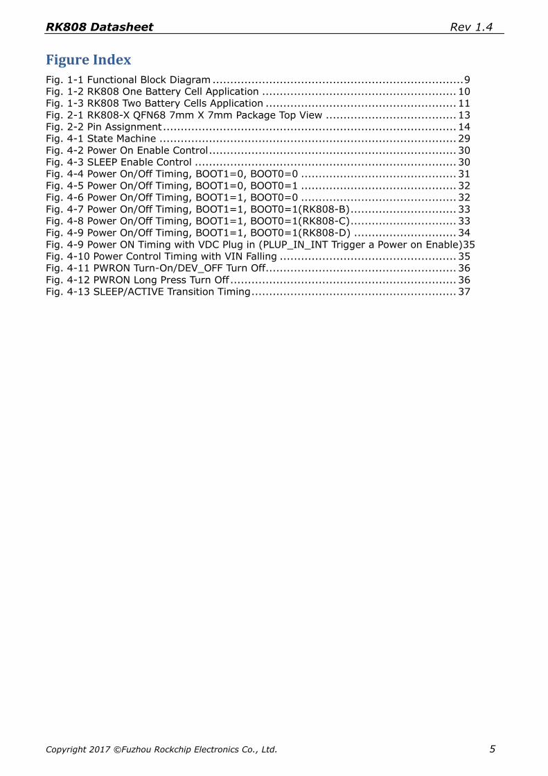
Figure Index
Fig. 1-1 Functional Block Diagram ....................................................................... 9 Fig. 1-2 RK808 One Battery Cell Application ....................................................... 10 Fig. 1-3 RK808 Two Battery Cells Application ...................................................... 11
Fig. 2-1 RK808-X QFN68 7mm X 7mm Package Top View ..................................... 13 Fig. 2-2 Pin Assignment ................................................................................... 14 Fig. 4-1 State Machine .................................................................................... 29
Fig. 4-2 Power On Enable Control ...................................................................... 30 Fig. 4-3 SLEEP Enable Control .......................................................................... 30 Fig. 4-4 Power On/Off Timing, BOOT1=0, BOOT0=0 ............................................ 31
Fig. 4-5 Power On/Off Timing, BOOT1=0, BOOT0=1 ............................................ 32 Fig. 4-6 Power On/Off Timing, BOOT1=1, BOOT0=0 ............................................ 32
Fig. 4-7 Power On/Off Timing, BOOT1=1, BOOT0=1(RK808-B) .............................. 33 Fig. 4-8 Power On/Off Timing, BOOT1=1, BOOT0=1(RK808-C) .............................. 33 Fig. 4-9 Power On/Off Timing, BOOT1=1, BOOT0=1(RK808-D) ............................. 34
Fig. 4-9 Power ON Timing with VDC Plug in (PLUP_IN_INT Trigger a Power on Enable)35 Fig. 4-10 Power Control Timing with VIN Falling .................................................. 35 Fig. 4-11 PWRON Turn-On/DEV_OFF Turn Off ...................................................... 36
Fig. 4-12 PWRON Long Press Turn Off ................................................................ 36 Fig. 4-13 SLEEP/ACTIVE Transition Timing .......................................................... 37

RK808 Datasheet Rev 1.4
Copyright 2017 ©Fuzhou Rockchip Electronics Co., Ltd. 6
Table Index
Table 4-1 Power Start Up Sequence ................................................................... 31 Table 4-2 Boot Timing Characteristics ................................................................ 34 Table 4-4 Vin and PLUG_IN Timing Characteristics ............................................... 36
Table 4-3 PWRON/DEV_OFF Timing Characteristics .............................................. 37 Table 4-4 SLEEP Timing Characteristics .............................................................. 37 Table 6-1 Thermal Resistance Characteristics ...................................................... 68

RK808 Datasheet Rev 1.4
Copyright 2017 ©Fuzhou Rockchip Electronics Co., Ltd. 7
Warranty Disclaimer Rockchip Electronics Co., Ltd makes no warranty, representation or guarantee (expressed, implied, statutory, or otherwise) by or with respect to anything in this document, and shall not be liable for any implied warranties of non-infringement, merchantability or fitness for a particular purpose or for any indirect, special or consequential damages. Information furnished is believed to be accurate and reliable. However, Rockchip Electronics Co., Ltd assumes no responsibility for the consequences of use of such information or for any infringement of patents or other rights of third parties that may result from its use. Rockchip Electronics Co., Ltd’s products are not designed, intended, or authorized for using as components in systems intended for surgical implant into the body, or other applications intended to support or sustain life, or for any other application in which the failure of the Rockchip Electronics Co., Ltd’s product could create a situation where personal injury or death may occur, should buyer purchase or use Rockchip Electronics Co., Ltd’s products for any such unintended or unauthorized application, buyers shall indemnify and hold Rockchip Electronics Co., Ltd and its officers, employees, subsidiaries, affiliates, and distributors harmless against all claims, costs, damages, expenses, and reasonable attorney fees arising out of, either directly or indirectly, any claim of personal injury or death that may be associated with such unintended or unauthorized use, even if such claim alleges that Rockchip Electronics Co., Ltd was negligent regarding the design or manufacture of the part.
Copyright and Patent Right Information in this document is provided solely to enable system and software implementers to use Rockchip Electronics Co., Ltd ’s products. There are no expressed or implied copyright licenses granted hereunder to design or fabricate any integrated circuits or integrated circuits based on the information in this document.
Rockchip Electronics Co., Ltd does not convey any license under its patent rights nor the rights of others.
All copyright and patent rights referenced in this document belong to their respective owners and shall be subject to corresponding copyright and patent licensing requirements.
Trademarks Rockchip and RockchipTM logo and the name of Rockchip Electronics Co., Ltd’s products are trademarks of Rockchip Electronics Co., Ltd. and are exclusively owned by Rockchip Electronics Co., Ltd. References to other companies and their products use trademarks owned by the respective companies and are for reference purpose only.
Confidentiality The information contained herein (including any attachments) is confidential. The recipient hereby acknowledges the confidentiality of this document, and except for the specific purpose, this document shall not be disclosed to any third party.
Reverse engineering or disassembly is prohibited. ROCKCHIP ELECTRONICS CO.,LTD. RESERVES THE RIGHT TO MAKE CHANGES IN ITS PRODUCTS OR PRODUCT SPECIFICATIONS WITH THE INTENT TO IMPROVE FUNCTION OR DESIGN AT ANY TIME AND WITHOUT NOTICE AND IS NOT REQUIRED TO UNDATE THIS DOCUMENTATION TO REFLECT SUCH CHANGES.
Copyright © 2017 Rockchip Electronics Co., Ltd. All rights reserved. No part of this publication may be reproduced, stored in a retrieval system, or transmitted in any form or by any means, electric or mechanical, by photocopying, recording, or otherwise, without the prior written consent of Rockchip Electronics Co., Ltd.

RK808 Datasheet Rev 1.4
Copyright 2017 ©Fuzhou Rockchip Electronics Co., Ltd. 8
Introduction
1.1 Overview
The RK808 is a complete power supply solution for Portable systems. The highly integrated
device includes four buck DC-DC converters, eight high performance ldos, two low Rds switches,
I2C interface, programmable power sequencing and an RTC.
The RK808 improves performance, reduces component count and size, and therefore provides
lower cost solution compared to conventional portable designs. The ultra fast 2MHz current
mode DC/DC architecture optimizes the transient performance and is compatible with tiny low
cost ceramic inductors and capacitors. All DC/DC channels include integrated MOSFETS.
Internal soft-start and compensation circuits minimize external components count. Most
outputs can be programmed through the I2C interface
1.2 Feature
Input voltage range: 2.7V to 5.5V
2MHz Switching Frequency for bucks
Current mode architecture for best transient performance
Internal compensation and soft start
I2C Programmable output levels and power sequencing
High efficiency architecture
Integrated Vout Discharge Circuit for BUCK and LDO
Power:
• CH1: Synchronous Buck regulator, 5A max
• CH2: Synchronous Buck regulator, 5A max
• CH3: Synchronous Buck regulator, 3A max
• CH4: Synchronous Buck regulator, 2.5A max
• CH6,CH7,CH9,CH11: Linear regulators, 150mA max
• CH8: Low noise and high PSRR linear regulator,100mA max
• CH10,CH12,CH13: Linear regulators, 300mA max
• CH14: Low Rds switch, 0.2ohm@Vgs=3v
• CH15: Low Rds switch, 0.2ohm@Vgs=3v
Auxiliary: Flexible Power Sequence control
Package: 7mmx7mm QFN68

RK808 Datasheet Rev 1.4
Copyright 2017 ©Fuzhou Rockchip Electronics Co., Ltd. 9
1.3 Block Diagram
BUCK1
Step-Down
5A
0.7125~1.5V
DAC
VCC1
SW1
GND1
BUCK3
Step-Down
3A
1.0~1.8V
VCC3
SW3
GND3
BUCK4
Step-Down
2.5A
1.8~3.3V
DAC
VCC4
SW4
GND4
LDO3
2MHz
Clock
LDO2
LDO4
LDO5
32K OSC
RTC
CLK32OUT1
OSC32KIN
OSC32KOUT
I2CSDA
SCK
INTSLEEP
PWRONExt_ENNRESPWRON
150mA
100mA
150mA
300mA
150mA
VCC6 LDO1
150mA
VCCA
VLDOA
Vdd_arm
BOOT0BOOT1
VREF
REFGND
DVSOK
Power
Sequence
Switch 1
300mA
Switch 2
300mA
LDO6
LDO7
300mA
300mA
LDO8
Vcc_tp
Vcca_33
Vcc_25
Vcc28_cif
Vcc_12
Vcc_lcd
Vcc_sd
Vdd_11
Vcc_io
Vcc_ddr
Vcc18_cif
Vcc33_wifi
LDO3
(low noise)
VCC9
VCC7
DVS1
DVS2
VCC12
VFB1
VFB3
VFB4
CLK32OUT2
Reference
CH1
CH3
CH4
CH6
CH7
CH8
CH13
CH9
CH10
CH11
CH12
CH14
CH15
VCC10
VCC11
VCC7
VDDIO
VCC8
VCCRTC
VCC1
SW1
GND1
BUCK1
Step-Down
5A
0.7125~1.5V
DAC
VCC2
SW2
GND2
Vdd_logic
VFB2
CH2
VCC2
SW2
GND2
Fig. 1-1 Functional Block Diagram

RK808 Datasheet Rev 1.4
Copyright 2017 ©Fuzhou Rockchip Electronics Co., Ltd. 10
1.4 Typical Application Diagrams
VCC64.7uF Vsys
VCCA4.7uF
Vccrtc
VDDIO4.7uF VCC_IO
VCCRTC4.7uFVccrtc
VLDOA2.2uF
VLDO12.2uF
VLDO22.2uFVcca_33
OSC32KIN22pF
22pF
OSC32KOUT
32.768K
SW1SW1
2.2uH
GND133uF
GND1
VDD_ARM
VFB1
SW3
VFB3
GND3
SW4
GND4
VFB4
VCC14.7uF
Vsys
VCC1
2.2uH
33uF
VCC_DDR
4.7uF
Vsys
VCC3
VCC42.2uH
33uF
VCC_IO
4.7uF
Vsys
Vcc_tp
VCC74.7uF
VCC_IO
VLDO32.2uF
VLDO74.7uF
Vcc18_cif
Vdd_11
VCC84.7uF
VSWOUT12.2uF Vcc_sd
VCC94.7uF
VLDO42.2uFVcc_25
VLDO52.2uF
Vcc28_cif
VCC104.7uF
VLDO62.2uFVcc_12
VCC114.7uF
VLDO82.2uF
Vcc33_wifi
VCC124.7uF
VSWOUT22.2uFVcc_lcd
CLK32KOUT2
CLK32KOUT1
VDC
VREF0.1uF
REFGND
AGND
DGND
DVS1DVS1
DVS2DVS2
DVSOK
SLEEPSLEEP
INT
NRESPWON
PWRONPWRON
10K
BOOT0BOOT0
BOOT1BOOT1
10K
AP
Power
Path
BATVsys
USB/AdapterEXT_EN
(VCC_IO)
VCC_IO
VCC_IO
VCC_IO
VCC_IO
VCC_IO
200K
33K
SCL
4.7K
SDA
4.7K
SCL
SDA
WIFI/BT
100K 100K 100K 100K
VCC_IO
VCC_IO
22nF
Vccrtc
Vccrtc
VCCIO_WIFI/BT
100K
SW2SW2
2.2uH
GND233uF
GND2
VDD_LOGIC
VFB1
VCC24.7uF
Vsys
VCC2
Vccrtc VPPOTP
RESET10K
Vccrtc
10K
Vccrtc
Fig. 1-2 RK808 One Battery Cell Application

RK808 Datasheet Rev 1.4
Copyright 2017 ©Fuzhou Rockchip Electronics Co., Ltd. 11
VCC64.7uF Vsys
VCCA4.7uF
VDDIO4.7uF VCC_IO
VCCRTC4.7uF
VLDOA2.2uF
VLDO12.2uF
VLDO22.2uFVcca_33
OSC32KIN22pF
22pF
OSC32KOUT
32.768K
SW1SW1
2.2uH
GND133uF
GND2
VDD_ARM
VFB1
SW4
GND4
VFB4
VCC14.7uF
Vsys
VCC1
VCC42.2uH
33uF
VCC_IO
4.7uF
Vsys
Vcc_tp
VCC74.7uF
VCC_IO
VLDO32.2uF
VLDO74.7uF
Vcc18_cif
Vdd_11
VCC84.7uF
VSWOUT12.2uF Vcc_sd
VCC94.7uF
VLDO42.2uFVcc_25
VLDO52.2uF
Vcc28_cif
VCC104.7uF
VLDO62.2uFVcc_12
VCC114.7uF
VLDO82.2uF
Vcc33_wifi
VCC124.7uF
VSWOUT22.2uFVcc_lcd
CLK32KOUT2
CLK32KOUT1
VDC
VREF0.1uF
REFGND
AGND
DGND
DVS1DVS1
DVS2DVS2
DVSOK
SLEEPSLEEP
INT
NRESPWON
PWRONPWRON
10K
BOOT0BOOT0
BOOT1BOOT1
10K
AP
Power
Path
2*BATVsys
9V/12V
Adapter
Ext_en
(VCC_IO)
VCC_IO
VCC_IO
VCC_IO
VCC_IO
VCC_IO
400K
33K
SCL
4.7K
SDA
4.7K
SCL
SDA
WIFI/BT
100K 100K 100K 100K
VCC_IO
VCC_IO
BUCK
LDO
SW3
VFB3
GND3
2.2uH
33uF
VCC_DDR
4.7uF
Vsys
VCC3
Vccrtc
Vccrtc
VCCIO_WIFI/BT
100K
22nF
SW2SW2
2.2uH
GND233uF
GND2
VDD_LOGIC
VFB2
VCC24.7uF
Vsys
VCC2
Vccrtc VPPOTP
RESET10K
10K
Vccrtc
Vccrtc
Vhvldo
Vsys must less than (Vccrtc+0.5V)
Fig. 1-3 RK808 Two Battery Cells Application

RK808 Datasheet Rev 1.4
Copyright 2017 ©Fuzhou Rockchip Electronics Co., Ltd. 12
Package information
2.1 Ordering information
Orderable
Device
RoHS
status
Package Package Qty Device
special
feature
RK808-B RoHS pass QFN68(7X7) 2600ea/inner box* 6
inner boxes/outer box
For
RK3288/RK3368
application
RK808-C RoHS pass QFN68(7X7) 2600ea/inner box* 6
inner boxes/outer box
For RK3288 C
application
RK808-D RoHS pass QFN68(7X7) 2600ea/inner box* 6
inner boxes/outer box
For RK3399
application
2.2 Top Marking
Rockchip: Brand Name
RKXXXX: Chip Name
ABC: Subcontractor CodeXXXXXX: Die Lot NO#DEFG: Date Code The first pin
Rockchip: Brand Name
RKXXXX: Chip Name
ABC: Subcontractor CodeXXXXXX: Die Lot NO#DEFG: Date Code The first pin

RK808 Datasheet Rev 1.4
Copyright 2017 ©Fuzhou Rockchip Electronics Co., Ltd. 13
Rockchip: Brand Name
RKXXXX: Chip Name
ABC: Subcontractor CodeXXXXXX: Die Lot NO#DEFG: Date Code The first pin
2.3 Dimension
Fig. 2-1 RK808-X QFN68 7mm X 7mm Package Top View

RK808 Datasheet Rev 1.4
Copyright 2017 ©Fuzhou Rockchip Electronics Co., Ltd. 14
DESCRIPTION SYMBOL MILLIMETER
MIN NOM MAX
TOTAL THICKNESS A 0.70 0.75 0.80
STAND OFF A1 0 0.035 0.05
MOLD THICKNESS A2 - 0.55 0.57
MATERIAL THICKNESS A3 - 0.203REF -
PACKAGE SIZE D - 7BSC -
E - 7BSC -
EP SIZE D1 5.39 5.49 5.59
E1 5.39 5.49 5.59
LEAD LENGTH L 0.30 0.4 0.50
LEAD PITCH e 0.35BSC
LEAD WIDTH b 0.1 0.15 0.2
LEAD OSITION OFFSET aaa 0.07
LEAD COPLANARITY bbb 0.08
PACKAGE EDGE PROFILE ccc 0.10
MOLD FLATNESS ddd 0.10
EP POSITION OFFSET eee 0.10
fff 0.05
Note:
Coplanarity applies to leads, corner leads and die attach pad. Dimension b applies to metalized terminal and is measured between 0.15mm and 0.30mm from the
terminal tip. If the terminal has the optional radius on the other end of the terminal, the dimension b
should not be measure in that radius area. 0.15mm of dimension b is recommended in PCB layout.
2.4 Pin Assignment
1
2
3
4
5
6
7
8
10
11
12
13
14
15
9
16
17
18
19
20
21
22
23
24
25
27
28
29
30
31
32
26
33
34
51
50
49
48
47
46
45
44
42
41
40
39
38
37
43
36
35
68
67
66
65
64
63
62
61
59
58
57
56
55
54
60
53
52
QFN68 7×7
VCC10
VLDO6
VCC7
VLDO3
VPPOTP
VSWOUT1
VCCRTC
VCC8
VCC12
VSWOUT2
VCC9
VLDO4
VLDO5
VLDO8
VDDIO
VCC11
VLDO7
SLEEP
INT
GND5
NC
VF
B3
GN
D3
VC
C3
SW
3
VC
C4
SW
4
VF
B4
GN
D4
EX
T_
EN
VREF
VLDOA
VD
C
NC
SD
A
SC
L
DV
S1
NR
ES
PW
RO
N
VC
C2
VC
C2
SW
2
SW
2
GN
D2
GN
D2
AG
ND
VF
B2
VL
DO
1
VC
C6
VCCA
VL
DO
2
DV
S2
CL
K3
2K
OU
T1
CL
K3
2K
OU
T2
RE
FG
ND
OS
C3
2K
OU
T
VCC1
VCC1
SW1
SW1
GND1
GND1
DGND
VFB1
DV
SO
K
BO
OT
1
PWRON
BO
OT
0
OS
C3
2K
IN
GND
Fig. 2-2 Pin Assignment

RK808 Datasheet Rev 1.4
Copyright 2017 ©Fuzhou Rockchip Electronics Co., Ltd. 15
2.5 Pinout Number Order
NO NAME SUPPLIES FUNCTIONAL
TYPE I/O DESCRIPTION BLOCK
9 VCCRTC VCCRTC
RTC
Power I RTC power supply /AGND
65 OSC32KIN VCCRTC
/DGND Analog I 32KHz crystal oscillator input
66 OSC32KOUT VCCRTC
/DGND Analog O 32KHz crystal oscillator output
68 CLK32KOUT1 VCCRTC
/DGND Digital O
32KHz clock output 1,OD output
(always on)
67 CLK32KOUT2 VCCRTC
/DGND Digital O 32KHz clock output 2,OD output
37 VREF VCCA
REFERENCE Analog O bandgap voltage
/REFGND
64 VREFGND REFGND Analog Gnd reference ground
36 VCCA VCCA
Analog Power Power I power supply for /GNDA
6 VPPOTP VPPOTP
Analog Power Power I OTP power supply /GNDA
45 VCC1 VCC1
BUCK1
Power I buck1 dc-dc power
supply /GND1
44 VCC1 VCC1
Power I buck1 dc-dc power
supply /GND1
43 SW1 VCC1
Power I/O buck1 dc-dc switch
output
/GND1
42 SW1 VCC1
/GND1
41 GND1 VCC1
Power Gnd buck1 dc-dc switch
ground
/GND1
40 GND1 VCC1
/GND1
39 VFB1 VCC1
Analog I buck1 dc-dc switch
feedback voltage /REFGND
23 VCC2 VCC2
BUCK2
Power I buck2 dc-dc power
supply /GND2
24 VCC2 VCC2
Power I buck2 dc-dc power
supply /GND2
25 SW2 VCC2
Power I/O buck2 dc-dc switch
output /GND2
26 SW2 VCC2
Power I/O buck2 dc-dc switch
output /GND2

RK808 Datasheet Rev 1.4
Copyright 2017 ©Fuzhou Rockchip Electronics Co., Ltd. 16
NO NAME SUPPLIES FUNCTIONAL
TYPE I/O DESCRIPTION BLOCK
27 GND2 VCC2
Power Gnd buck2 dc-dc switch
ground /GND2
28 GND2 VCC2
Power Gnd buck2 dc-dc switch
ground /GND2
29 VFB2 VCC2
Analog I buck2 dc-dc switch
feedback voltage /REFGND
59 VCC3 VCC3
BUCK3
Power I buck3 dc-dc power
supply /GND3
58 SW3 VCC3
Power I/O buck3 dc-dc switch
output /GND3
57 GND3 VCC3
Power Gnd buck3 dc-dc switch
ground /GND3
56 VFB3 VCC3
Analog I buck3 dc-dc switch
feedback voltage /REFGND
60 VCC4 VCC4
BUCK4
Power I buck4 dc-dc power
supply /GND4
61 SW4 VCC4
Power I/O buck4 dc-dc switch
output /GND4
62 GND4 VCC4
Power Gnd buck4 dc-dc switch
ground /GND4
63 VFB4 VCC4
Analog I buck4 dc-dc switch
feedback voltage /REFGND
47 NC
46 GND5 VCCA
Power Gnd ground
/GND5
48 NC
32 VCC6 VCC6 LDO 1~8,
Power I LDO1,LDO2 power
supply /AGND SWITCH1,2
4 VCC7 VCC7
Power I LDO3,LDO7 power
supply /AGND
8 VCC8 VCC8
Power I SWITCH1 power
supply /AGND
13 VCC9 VCC9
Power I LDO4,LDO5 power
supply /AGND
1 VCC10 VCC11
Power I LDO6 power supply /AGND
16 VCC11 VCC11
Power I LDO8 power supply /AGND
10 VCC12 VCC12
Power I SWITCH2 power
supply /AGND
31 VLDO1 VCC7
Power O LDO1 regulator output /AGND
33 VLDO2 VCC7 Power O LDO2 regulator output

RK808 Datasheet Rev 1.4
Copyright 2017 ©Fuzhou Rockchip Electronics Co., Ltd. 17
NO NAME SUPPLIES FUNCTIONAL
TYPE I/O DESCRIPTION BLOCK
/AGND
3 VLDO3 VCC8
Power O LDO3 regulator output /AGND
12 VLDO4 VCC9
Power O LDO4 regulator output /AGND
14 VLDO5 VCC10
Power O LDO5 regulator output /AGND
2 VLDO6 VCC9
Power O LDO6 regulator output /AGND
5 VLDO7 VCC1
Power O LDO7 regulator output 1/AGND
15 VLDO8 VCC11
Power O LDO8 regulator output /AGND
7 VSWOUT1 VCC8
Power O Switch 1 output /AGND
11 VSWOUT2 VCC12
Power O Switch 2 output /AGND
30 AGND POWER PAD Analog ground Power Gnd Analog ground
35 VLDOA POWER PAD LDOA Power I supply for internal analog circuit
38 DGND POWER PAD Digital ground Power Gnd Digital ground
17 VDDIO VDDIO
IO
Power I Digital I/O power supply /DGND
50 SLEEP
VDDIO
Digital I Active-Sleep state
transition control signal /DGND
20 NRESPWRON
VDDIO
Digital O Power off reset for AP/
External reset digital core(excludes RTC)
/DGND
49 INT
VDDIO
IO
Digital O Interrupt flag (polarity
is I2C programmable, default active high)
/DGND
51 PWRON
VCCRTC
Digital I External switch-on
control signal(ON button) /DGND
18 SDA VDDIO
Digital I/O I2C data signal /DGND
19 SCL VDDIO
Digital I/O I2C clock signal /DGND
52 BOOT0 VCCRTC
/DGND IO
Digital I Power-up sequence selection
53 BOOT1 VCCRTC
/DGND Digital I Power-up sequence selection

RK808 Datasheet Rev 1.4
Copyright 2017 ©Fuzhou Rockchip Electronics Co., Ltd. 18
NO NAME SUPPLIES FUNCTIONAL
TYPE I/O DESCRIPTION BLOCK
55 EXT_EN VCCRTC
/DGND Digital O
Output enable for
external BUCK in two-battery-
cells
application
22 DVS1
VDDIO
Digital I
BUCK1 DVS voltage
/normal voltage transition control
signal(polarity is
I2C programmable, default active high) /DGND
21
DVS2
VDDIO
Digital
I
BUCK2 DVS voltage
/normal voltage transition control
signal(polarity is
I2C programmable, default active high)
/DGND
54 DVSOK VDDIO
Digital O BUCK1 and BUCK2 power good
flag after dynamic voltage setting /DGND
34 VDC VDC
Digital I Adapter voltage detect input /AGND

RK808 Datasheet Rev 1.4
Copyright 2017 ©Fuzhou Rockchip Electronics Co., Ltd. 19
Electrical Characteristics
3.1 Absolute Maximum Ratings
Parameter Min Max Uni
ts
Voltage range on pins VCCx, VDDIO, VCCRTC,
VFBx, VLDOx, VSWOUTx, VREF
-0.3 7 V
Voltage range on pin CLK32KOUT1,
CLK32KOUT2, VDC, SLEEP
-0.3 7 V
Voltage range on pins OSC32KIN, OSC32KOUT,
BOOT0, BOOT1, EXT_EN, PWRON
-0.3 VCCRTCMAX+0.3
Voltage range on pins NRESPWRON, INT, SDA,
SCL, DVS1, DVS2, DVSOK
-0.3 VDDIO+0.3 V
Storage temperature range, TS -40 150 ℃
Operating temperature range, TJ -40 125 ℃
Maximum Soldering Temperature, TSOLDER 260 ℃
Note 1. Exposure to the conditions exceeded absolute maximum ratings may cause the permanent
damages and affect the reliability and safety of both device and systems using the device. The
functional operations cannot be guaranteed beyond specified values in the recommended conditions.
3.2 Recommended Operating Conditions
Parameter Min TYP Max Units
Voltage range on pins VCCx 3 5.5 V
Voltage range on pins VDDIO 1.8 5.5 V
Voltage range on pin VCCRTC 2.5 5.5 V
Voltage range on other pins 5.5 V
Power Dissipation 2.5 W
3.3 DC Characteristics
TJ=25C; VBAT=VCCx=3.8V, VDDIO=3V unless otherwise specified.
Parameter Symbol Min. Typ. Max. Unit
General
Input supply voltage range ( VBAT ) VINPUT 2.7 5.5 V
Battery low alarm voltage
(2.8V~3.5V programmable, step=100mV) VBLO 3.25 3.3 3.35 V
Battery under voltage threshold (vin falling) VBUVL 2.5 V
Battery under voltage threshold (vin rising) VBUVH 2.6 2.7 2.8 V
Battery OK voltage threshold
(3.0V/3.4V/3.5V/3.6V OTP programmable)
VBOK 3.0 V
Power on Reset Threshold (Rising) VPORH 2.2 V

RK808 Datasheet Rev 1.4
Copyright 2017 ©Fuzhou Rockchip Electronics Co., Ltd. 20
Parameter Symbol Min. Typ. Max. Unit
Power on Reset Threshold (Falling) VPORL 1.2 V
Over Voltage Lock Out Threshold (Vin Rising) VTH(OVLO) 5.7 6.0 6.3 V
Over Voltage Lock Out Hysteresis VHYS (OVLO) 0.2 V
VDC pin threshold(rising edge) VDCH 0.6 V
VDC pin threshold(falling edge) VDCL 0.54 V
Stand-by current, VDD=3.6V, device OFF state
32KHz clock running
IQ(STNBY) 60 uA
Hot-die temperature rising threshold
(85℃~115℃ programmable, step=10℃) THD 85 115 ℃
Thermal shut down
(140℃~170℃ programmable, step=30℃)
TTSD 140 170 ℃
Oscillator circuit
Switching Frequency CH1,2,3,4( Tj=25℃ ) fSW 1.8 2 2.2 MHz
Logic inputs
Input LOW-Level Voltage (VDDIO) VIL 0.3xVDDIO V
Input HIGH-Level Voltage (VDDIO) VIH 0.7xVDDIO V
Logic outputs
LOW-Level Output Voltage, 3.0 mA sink
current
VOL 0.4 V
HIGH-Level Output Voltage, 3.0 mA source
current
VOH VDDIO-0.4 V
NRESPWON pin LOW-Level Output Voltage,
3.0mA sink current
VOL(NRES) 0.4 V
CLK32KOUT1 pin LOW-Level Output Voltage,
3.0mA sink current
VOL(CLKO1) 0.4 V
CLK32KOUT2 pin LOW-Level Output Voltage,
3.0mA sink current
VOL(CLKO2) 0.4
CLK32KOUT2 pin HIGH-Level Output
Voltage, 3.0mA source current
VOH(CLKO2) VCCRTC-0.4 V
CH1 Buck1 Regulator
Input supply voltage range VINPUT1 2.7 5.5 V
Voltage Adjustable Range, 6bit VFB1 0.7125 1.500 V
DC output voltage programmable step(DVS) 12.5 mV
Output voltage transition rate
BUCK1_RATE=00
BUCK1_RATE=01
BUCK1_RATE=10
BUCK1_RATE=11
2
3.6
5
6.5
mV/us
DVS OK threshold (Vout rising) VDVSOKR1 93 %
DVS OK threshold (Vout falling) VDVSOKF1 107 %
Power Good threshold (Vout rising) VPG1 93 %
Output under voltage lockout(Vout falling) VUV1 85 %
Output over voltage lockout (Vout rising) VOV1 117 %

RK808 Datasheet Rev 1.4
Copyright 2017 ©Fuzhou Rockchip Electronics Co., Ltd. 21
Parameter Symbol Min. Typ. Max. Unit
Preset Voltage, Default( Tj=25℃ ) VFB1(Default) 1.078 1.100 1.122 V
Preset Voltage, Default(-10℃≦Tj≦+85℃) VFB1(Default) 1.067 1.100 1.133 V
Load Regulation, IOUT1 = 100mA to 5A 1 %/A
Line Regulation, VCC1 = 3 to 5V, IOUT1 = 1A 0.1 %/V
Rated output current(If ICL1=6A) IMAX1 5 A
Switch Current Limit
(4.5A~6A programmable, step=0.5A)
ICL1 6 A
Operating Quiescent Current, No load,
VDD=3.8V
IQ1 70 uA
Minimun Switch Current Limit
(50mA~400mA programmable, step=50mA)
ICLMIN1 100 mA
Soft-start Time tSS1 400 us
COUT Discharge Switch ON Resistance RDIS1 400 ohm
Conversion Effeciency (Vin=3.8V,Vout=1.1V)
Iout=5A
Iout=4A
Iout=3A
Iout=2A
Iout=1 A
Iout=500mA
Iout=100 mA
Iout=10 mA
68
73
78
84
89
90
81
79
%
CH2 Buck2 Regulator
Input supply voltage range VINPUT2 2.7 5.5 VINPUT2
Voltage Adjustable Range, 6bit VFB2 0.7125 1.500 VFB2
DC output voltage programmable step(DVS) 12.5
Output voltage transition rate
BUCK2_RATE=00
BUCK2_RATE=01
BUCK2_RATE=10
BUCK2_RATE=11
2
3.6
5
6.5
DVS OK threshold (Vout rising) VDVSOKR2 93 %
DVS OK threshold (Vout falling) VDVSOKF2 107 %
Power Good threshold (Vout rising) VPG2 93 %
Output under voltage lockout (Vout falling) VUV2 85 %
Output over voltage lockout (Vout rising) VOV2 117 %
Preset Voltage, Default( Tj=25℃ ) VFB2(Default) 1.078 1.100 V
Preset Voltage, Default(-10℃≦Tj≦+85℃) VFB2(Default) 1.067 1.100 V
Load Regulation, IOUT2 = 100 mA to 5A 1 %/A
Line Regulation, VCC2 = 3 to 5V, IOUT2 = 1A 0.1 %/V
Rated output current(If ICL2=6A) IMAX2 5 A

RK808 Datasheet Rev 1.4
Copyright 2017 ©Fuzhou Rockchip Electronics Co., Ltd. 22
Parameter Symbol Min. Typ. Max. Unit
Switch Current Limit
(4.5A~6A programmable, step=0.5A)
ICL2 6 A
Operating Quiescent Current, No load,
VDD=3.8V
IQ2 70 uA
Minimun Switch Current Limit
(50mA~400mA programmable, step=50mA)
ICLMIN2 100 mA
Soft-start Time tSS2 400 us
COUT Discharge Switch ON Resistance RDIS2 400 ohm
Conversion Effeciency (Vin=3.8V,Vout=1.1V)
Iout=5A
Iout=4A
Iout=3A
Iout=2A
Iout=1 A
Iout=500mA
Iout=100 mA
Iout=10 mA
68
73
78
84
89
90
81
79
%
CH3 Buck3 Regulator
Input supply voltage range VINPUT3 2.7 5.5 V
Feedback Voltage, Default( Tj=25℃ ) VFB3(Default) 0.98 1.00 V
Feedback Voltage, Default(-10℃≦Tj≦+85℃) VFB3(Default) 0.97 1.00 V
Power Good threshold (Vout rising) VPG3 93 %
Output under voltage lockout (Vout falling) VUV3 85 %
Output over voltage lockout (Vout rising) VOV3 117 %
Load Regulation, IOUT3 = 100mA to 3A 1 %/A
Line Regulation, VCC3 = 3 to 5V, IOUT3 = 0.5A 0.1 %/V
Rated output current(If ICL3=3.5A) IMAX3 3 A
Switch Current Limit
(2A~3.5A programmable, step=0.5A)
ICL3 3.5 A
Operating Quiescent Current, No load,
VDD=3.8V
IQ3 70 uA
Minimun Switch Current Limit
(50mA~400mA programmable, step=50mA)
ICLMIN3 100 mA
Soft-start Time tSS3 400 us
COUT Discharge Switch ON Resistance RDIS3 250 ohm
Conversion Effeciency (Vin=3.8V,Vout=1.4V)
Iout=3A
Iout=2A
Iout=1.5A
71
79
83
%

RK808 Datasheet Rev 1.4
Copyright 2017 ©Fuzhou Rockchip Electronics Co., Ltd. 23
Parameter Symbol Min. Typ. Max. Unit
Iout=1 A
Iout=500mA
Iout=100 mA
Iout=10 mA
87
90
83
76
CH4 Buck4 Regulator
Input supply voltage range VINPUT4 2.7 5.5 V
Voltage Adjustable Range, 4bit VFB4 1.8 3.3 V
DC output voltage programmable step(gain
select)
100 mV
Feedback Voltage, Default( Tj=25℃ ) VFB4(Default) 2.94 3.00 3.06 V
Feedback Voltage, Default(-10℃≦Tj≦+85℃) VFB4(Default) -2.91 3.00 3.09 V
Power Good threshold (Vout rising) VPG4 93 %
Output under voltage lockout (Vout falling) VUV4 85 %
Output over voltage lockout (Vout rising) VOV4 117 %
Load Regulation, IOUT4 = 100mA to 2.5A 1 %/A
Line Regulation, VCC4 = 3 to 5V, IOUT4 = 0.5A 0.1 %/V
Rated output current(If ICL4=3.5A) IMAX4 2.5 A
Switch Current Limit
(2A~3.5A programmable, step=0.5A)
ICL4 3.5 A
Operating Quiescent Current, No load,
VDD=3.8V
IQ4 70 uA
Minimun Switch Current Limit
(50mA~400mA programmable, step=50mA)
ICLMIN4 100 mA
Soft-start Time tSS4 400 us
COUT Discharge Switch ON Resistance RDIS4 400 Ohm
Conversion Effeciency, (DCR<50mohm)
Vin=3.8V,Vout=3V
Iout=2.5A
Iout=2A
Iout=1 .5A
Iout=1 A
Iout=500mA
Iout=100mA
Iout=10mA
85
89
91
94
95
92
60
%
CH6 LDO1
Input supply voltage range VINPUT6 2.7 5.5 V
VOUT Output Voltage Adjustable Range,
4bit(step=100mv)
VOUT6 1.8 3.4 V
VOUT Output Voltage, Default( Tj=25℃ ) VOUT6(Default) 3.234 3.300 3.366 V

RK808 Datasheet Rev 1.4
Copyright 2017 ©Fuzhou Rockchip Electronics Co., Ltd. 24
Parameter Symbol Min. Typ. Max. Unit
VOUT Output Voltage, Default( Tj= -10~85℃ ) VOUT6(Default) 3.201 3.300 3.399 V
Power Good threshold (Vout rising) VPG6 93 %
Output under voltage lockout (Vout falling) VUV6 85 %
VOUT Load Regulation, IOUT = 1mA to 150mA 0.005 %/mA
VOUT Line Regulation, VIN6 = 3 to 5V, IOUT6 =
0.1A
0.03 %/V
Power Supply Reject Ratio (f = 10kHz,
VOUT6=3.3V)
PSRR6 50 dB
Output noise (10Hz to 100kHz, VOUT6=3.3V) OUTNOISE6 300 uVrms
Dropout voltage @ 150mA (VOUT6=3.3V) VDROP6 200 mV
Rated output current IMAX6 150 mA
Operating Quiescent Current, No load,
VDD=3.8V
IQ6 28 uA
Current Limit, VOUT6 = VOUT6 x 0.95 ICL6 250 300 mA
Soft-start Time tSS6 400 us
COUT Discharge Switch ON Resistance RDIS6 400 ohm
CH7 LDO2
Input supply voltage range VINPUT7 2.7 5.5 V
VOUT Output Voltage Adjustable Range,
4bit(step=100mv)
VOUT7 1.8 3.4 V
VOUT Output Voltage, Default( Tj=25℃ ) VOUT7(Default) 3.234 3.300 3.366 V
VOUT Output Voltage, Default( Tj=-10~85℃ ) VOUT7(Default) 3.201 3.300 3.399 V
Power Good threshold (Vout rising) VPG7 93 %
Output under voltage lockout (Vout falling) VUV7 85 %
VOUT Load Regulation, IOUT = 1mA to 150mA 0.005 %/mA
VOUT Line Regulation, VIN7= 3 to 5V, IOUT7 =
0.1A
0.03 %/V
Power Supply Reject Ratio (f = 10kHz,
VOUT7=3.3V)
PSRR7 50 dB
Output noise (10Hz to 100kHz, VOUT7=3.3V) OUTNOISE7 300 uVrms
Dropout voltage @ 150mA (VOUT7=3.3V) VDROP7 200 mV
Operating Quiescent Current, No load,
VDD=3.8V
IQ7 28 uA
Rated output current IMAX7 150 mA
Current Limit, VOUT7 = VOUT7 x 0.95 ICL7 250 300 mA
Soft-start Time tSS7 400 us
COUT Discharge Switch ON Resistance RDIS7 400 Ohm
CH8 LDO3
Input supply voltage range VINPUT7 2.7 5.5 V
VOUT Output Voltage Adjustable Range,
4bit (0.8V~2V, step=100mV, 2V~ 2.5V
step=500mV)
VOUT8 0.8 2.5 V
VOUT Output Voltage, Default( Tj=25℃ ) VOUT8(Default) 1.078 1.100 1.122 V
VOUT Output Voltage, Default( Tj=-10~85℃ ) VOUT8
(Default)
1.067 1.100 1.133 V

RK808 Datasheet Rev 1.4
Copyright 2017 ©Fuzhou Rockchip Electronics Co., Ltd. 25
Parameter Symbol Min. Typ. Max. Unit
Power Good threshold (Vout rising) VPG8 93 %
Output under voltage lockout (Vout falling) VUV8 85 %
VOUT Load Regulation, IOUT = 1mA to 150mA 0.006 %/mA
VOUT Line Regulation, VIN8 = 3 to 5V, IOUT8 =
0.05A
0.015 %/V
Power Supply Reject Ratio (f = 10kHz,
VOUT8=1.1V)
PSRR8 70 dB
Output noise (10Hz to 100kHz, VOUT8=1.1V) OUTNOISE8 30 uVrms
Dropout voltage @ 100mA (VOUT8=2.5V) VDROP8 200 mV
Rated output current IMAX8 100 mA
Operating Quiescent Current, No load,
VDD=3.8V
IQ8 52 uA
Current Limit, VOUT8 = VOUT8 x 0.95 ICL8 150 200 mA
Soft-start Time tSS8 400 us
COUT Discharge Switch ON Resistance RDIS8 400 Ohm
CH9 LDO4
Input supply voltage range VINPUT9 2.7 5.5 V
VOUT Output Voltage Adjustable Range,
4bit(step=100mv)
VOUT9 1.8 3.4 V
VOUT Output Voltage, Default( Tj=25℃ ) VOUT9(Default) 2.450 2.500 2.550 V
VOUT Output Voltage, Default( Tj=-10~85℃ ) VOUT9(Default) 2.425 2.500 2.575 V
Power Good threshold (Vout rising) VPG9 93 %
Output under voltage lockout (Vout falling) VUV9 85 %
VOUT Load Regulation, IOUT = 1mA to 150mA 0.005 %/mA
VOUT Line Regulation, VIN9 = 3 to 5V, IOUT9 =
0.15A
0.03 %/V
Power Supply Reject Ratio (f = 10kHz,
VOUT9=3.3V)
PSRR9 50 dB
Output noise (10Hz to 100kHz, VOUT9=3.3V) OUTNOISE9 300 uVrms
Dropout voltage @ 150mA (VOUT9=3.3V) VDROP9 200 mV
Operating Quiescent Current, No load,
VDD=3.8V
IQ9 28 uA
Rated output current IMAX9 150 mA
Current Limit, VOUT9 = VOUT9 x 0.95 ICL9 250 300 mA
Soft-start Time tSS9 400 us
COUT Discharge Switch ON Resistance RDIS9 400 Ohm
CH10 LDO5
Input supply voltage range VINPUT10 2.7 5.5 V
VOUT Output Voltage Adjustable Range,
4bit(step=100mv)
VOUT10 1.8 3.4 V
VOUT Output Voltage, Default( Tj=25℃ ) VOUT10(Default) 2.744 2.800 2.856 V
VOUT Output Voltage, Default( Tj=-10~85℃ ) VOUT10(Default) 2.716 2.800 2.884 V
Power Good threshold (Vout rising) VPG10 93 %
Output under voltage lockout (Vout falling) VUV10 85 %
VOUT Load Regulation, IOUT = 1mA to 300mA 0.003 %/mA

RK808 Datasheet Rev 1.4
Copyright 2017 ©Fuzhou Rockchip Electronics Co., Ltd. 26
Parameter Symbol Min. Typ. Max. Unit
VOUT Line Regulation, VIN10 = 3 to 5V, IOUT10 =
0.3A
0.01 %/V
Power Supply Reject Ratio (f = 10kHz,
VOUT10=3.3V)
PSRR10 52 dB
Output noise (10Hz to 100kHz, VOUT10=3.3V) OUTNOISE10 300 uVrms
Dropout voltage @ 300mA (VOUT10=2.8V) VDROP10 200 mV
Operating Quiescent Current, No load,
VDD=3.8V
IQ10 28 uA
Rated output current IMAX10 300 mA
Current Limit, VOUT10 = VOUT10 x 0.95 ICL10 350 500 mA
Soft-start Time tSS10 400 us
COUT Discharge Switch ON Resistance RDIS10 400 Ohm
CH11 LDO6
Input supply voltage range VINPUT11 2.7 5.5 V
VOUT Output Voltage Adjustable Range,
5bit(step=100mv)
VOUT11 0.8 2.5 V
VOUT Output Voltage, Default( Tj=25℃ ) VOUT11(Default) 1.176 1.200 1.224 V
VOUT Output Voltage, Default( Tj=-10~85℃ ) VOUT11(Default) 1.164 1.200 1.236 V
Power Good threshold (Vout rising) VPG11 93 %
Output under voltage lockout (Vout falling) VUV11 85 %
VOUT Load Regulation, IOUT = 1mA to 150mA 0.005 %/mA
VOUT Line Regulation, VIN11 = 3 to 5V, IOUT11 =
0.1A
0.015 %/V
Power Supply Reject Ratio (f = 10kHz,
VOUT11=3.3V)
PSRR11 70 dB
Output noise (10Hz to 100kHz, VOUT11=3.3V) OUTNOISE11 30 uVrms
Dropout voltage @ 150mA (VOUT11=2.5V) VDROP11 500 mV
Operating Quiescent Current, No load,
VDD=3.8V
IQ11 52 uA
Rated output current IMAX11 150 mA
Current Limit, VOUT11 = VOUT11 x 0.95 ICL11 200 300 mA
Soft-start Time tSS11 400 us
COUT Discharge Switch ON Resistance RDIS11 400 Ohm
CH12 LDO7
Input supply voltage rangef VINPUT12 2.7 5.5 V
VOUT Output Voltage Adjustable Range,
5bit(step=100mv)
VOUT12 0.8 2.5 V
VOUT Output Voltage, Default( Tj=25℃ ) VOUT12(Default) 1.764 1.800 1.836 V
VOUT Output Voltage, Default( Tj=-10~85℃ ) VOUT12(Default) -1.736 1.800 1.854 V
Power Good threshold (Vout rising) VPG12 93 %
Output under voltage lockout (Vout falling) VUV12 85 %
VOUT Load Regulation, IOUT = 1mA to 300mA 0.005 %/mA
VOUT Line Regulation, VIN12 = 3 to 5V, IOUT12 =
0.3A
0.015 %/V
Power Supply Reject Ratio (f = 10kHz, PSRR12 65 dB

RK808 Datasheet Rev 1.4
Copyright 2017 ©Fuzhou Rockchip Electronics Co., Ltd. 27
Parameter Symbol Min. Typ. Max. Unit
VOUT12=3.3V)
Output noise (10Hz to 100kHz, VOUT12=3.3V) OUTNOISE12 50 uVrms
Dropout voltage @ 300mA (VOUT12=2.5V) VDROP12 200 mV
Operating Quiescent Current, No load,
VDD=3.8V
IQ12 48 uA
Rated output current IMAX12 300 mA
Current Limit, VOUT12 = VOUT12 x 0.95 ICL12 400 400 mA
Soft-start Time tSS12 400 us
COUT Discharge Switch ON Resistance RDIS12 400 Ohm
CH13 LDO8
Input supply voltage range VINPUT13 2.7 5.5 V
VOUT Output Voltage Adjustable Range,
4bit(step=100mv)
VOUT13 1.8 3.4 V
VOUT Output Voltage, Default( Tj=25℃ ) VOUT13(Default) 3.234 3.300 3.366 V
VOUT Output Voltage, Default( Tj=-10~85℃ ) VOUT13(Default) 3.201 3.300 3.399 V
Power Good threshold (Vout rising) VPG13 93 %
Output under voltage lockout (Vout falling) VUV13 85 %
VOUT Load Regulation, IOUT = 1mA to 150mA 0.003 %/mA
VOUT Line Regulation, VIN13 = 3 to 5V, IOUT6 =
0.15A
0.01 %/V
Power Supply Reject Ratio (f = 10kHz,
VOUT13=3.3V)
PSRR13 50 dB
Output noise (10Hz to 100kHz, VOUT13=3.3V) OUTNOISE13 300 uVrms
Dropout voltage @ 300mA (VOUT13=2.8V) VDROP13 200 mV
Operating Quiescent Current, No load,
VDD=3.8V
IQ13 30 uA
Rated output current IMAX13 300 mA
Current Limit, VOUT13 = VOUT13 x 0.95 ICL13 400 500 mA
Soft-start Time tSS13 400 us
COUT Discharge Switch ON Resistance RDIS13 400 Ohm
CH14 SWITCH1
Input supply voltage range VINPUT14 2.7 5.5 V
Rated output current IMAX14 300 mA
On resistance( Vgs=3V) 200 mohm
Current Limit ICL14 400 500 mA
COUT Discharge Switch ON Resistance RDIS14 400 Ohm
CH15 SWITCH2
Input supply voltage range VINPUT15 2.7 5.5 V
Rated output current IMAX15 300 mA
On resistance( Vgs=3V) 200 mohm
Current Limit ICL15 400 500 mA
COUT Discharge Switch ON Resistance RDIS15 400 Ohm
Real Time Clock (RTC)

RK808 Datasheet Rev 1.4
Copyright 2017 ©Fuzhou Rockchip Electronics Co., Ltd. 28
Parameter Symbol Min. Typ. Max. Unit
RTC Operating Voltage Range VIN 2.5 5.5 V
RTC Supply Current IQ 5 uA
CLK32OUT1 jitter (open drain) (always on) -25 +25 ns
CLK32OUT1 duty cycle 40 60 %
CLK32OUT2 jitter (open drain) -25 +25 ns
CLK32OUT2 duty cycle 40 60 %
I2C Interface TIMING SPECIFICATIONS (7-bits Slave address: 0011011)
SCL clock frequency fSCL 400 kHz
SCL high time tHIGH 0.6 us
SCL low time tLOW 1.3 us
Data setup time tSU,DAT 0.1 us
Data hold time tHD,DAT1 0.3 us
Setup time for repeated start tSU,STA 0.6 us
HOLD time for start/repeated start tHD,STA 0.6 us
Rise time of SCL/SDA,CB =400pF tr 300 ns
Fall width of SCL/SDA,CB =400pF tf 300 ns
Pulse width of suppressed spike tSP 50 ns
Capacitive load for each of bus line CB 400 pF

RK808 Datasheet Rev 1.4
Copyright 2017 ©Fuzhou Rockchip Electronics Co., Ltd. 29
Function Description
4.1 State Machine Description
OFF
ACTIVE
SLEEP
POWER ON enabled
POWER ON disabled Sleep enabled
Sleep disabled
POWER ON disabled
Fig. 4-1 State Machine
4.2 Device Power on Enable Conditions
If none of the device power-on disable conditions is met, the following conditions are
available to turn on and/or maintain the ON state of the device: PWRON signal low level. Or interrupt flag active (INT low) while the device is off (NRESPWRON = 0)
The power-on enable condition occurs only if the interrupt status bit is initially low (no previous identical interrupt pending in the status register).
The Interrupt sources expected when the device is off are:
PWRON low-level interrupt (PWRON_INT = 1 in INT_STS_REG1 register) First VDC rising above plug-in threshold (PLUG_IN interrupt(PLUG_IN_INT=1 in
INT_STS_REG2 register) (Charger plug in interrupt)
The Interrupt source expected if enabled when the device is off is: RTC Alarm interrupt (INT_ALARM_EN=1 in RTC_INT_REG and RTC_ALARM_INT = 1
in INT_STS_REG register)

RK808 Datasheet Rev 1.4
Copyright 2017 ©Fuzhou Rockchip Electronics Co., Ltd. 30
PWRON
DEV_OFF
DEV_OFF_RST
PWRON_LP_INT
TSD
PWRON ON enable
2s
NRESPWRON
VB_UV
PLUG_IN_INT
RTC_ALARM_INT
VB_LO_STS
VB_LO_ACT
POWER OFF
POWER ON
POWER ON conditions(if non POWER OFF conditions exist):1. PWRON falling edge2. RTC_ALARM_INT=1(if RTC_ALARM_INT_IM=0) or PLUG_IN_INT=1(if PLUG_IN_INT_IM=0) when NRESPWRON=0
POWER OFF:1. DEV_OFF_RST=12. DEV_OFF=13. 2s delay after PWRON_LP_INT=14. VB_UV=15. TSD=16. VB_LO_STS=1 and if VB_LO_ACT=0
Fig. 4-2 Power On Enable Control
4.3 Device Power on Disable Conditions
PWRON signal low level during more than the long-press delay: TDPWRONLP. The
interrupt corresponding to this condition is PWRON_LP_INT in the INT_STS_REG register. Or Die temperature has reached the thermal shutdown threshold: TSD_STS=1 in
THERMAL_REG).
Or Vbat down below UVLO threshold: VB_UV_STS=1 in VB_MON_REG. Or DEV_OFF or DEV_OFF_RST control bit set to 1 (value of DEV_OFF is cleared when the
device is in OFF state).
4.4 Device Sleep Enable Conditions
SLEEP signal high level. OR DEV_SLP control bit set to 1 And interrupt flag inactive (INT high): No non-masked interrupt pending
The SLEEP state can be controlled by programming DEV_SLP and keeping the SLEEP state.
SLEEP enableSLEEP
DEV_SLP
INT
INT=1的条件:下面9种发生任意一种情况都会令INT=1
1. VOUT_INT=1(if VOUT_INT_IM=0)2. VB_LO_INT=1(if VB_LO_INT_IM=0)3. PWRON_INT=1(if PWRON_INT_IM=0)4. PWRON_LP_INT=1(if PWRON_LP_INT_IM=0)5. HOTDIE_INT=1(if HOTDIE_INT_IM=0)6. RTC_ALARM_INT=1(if RTC_ALARM_INT_IM=0)7. RTC_PERIOD_INT=1(if RTC_PERIOD_INT_IM=0)8. PLUG_IN_INT=1(if PLUG_IN_INT_IM=0)9. PLUG_OUT_INT=1(if PLUG_OUT_INT_IM=0)
Fig. 4-3 SLEEP Enable Control
4.5 Power Sequence

RK808 Datasheet Rev 1.4
Copyright 2017 ©Fuzhou Rockchip Electronics Co., Ltd. 31
Power On
Sequence
Preset
Voltage
Power On
Sequence
Preset
Voltage
Power On
Sequence
Preset
Voltage
Power On Sequence
Boot1/0 00 01 10
11
RK808-B RK808-C RK808-D
Sequence
Typ
Vout
Sequence
Typ
Vout
Sequence
Typ
Vout
Sequence
Typ
Vout
Sequence
Typ
Vout
Sequence
Typ
Vout
BUCK1 4 1.1V 4 1.2V 4 1.0V 2 1.1V 2 1.0V 4 0.9V
BUCK2 5 1.1V 5 1.2V 4 1.0V 3 1.1V 3 1.0V 3 0.9V
BUCK3 2 X* 2 X* 3 X* 3 X* 4 X* 2 X*
BUCK4 1 3.0V 1 3.0V 1 3.0V 4 3.3V 6 1.8V 1 1.8V
LDO1 OFF 3.3V OFF 3.3V 1 3.3V 4 1.8V 7 3.3V OFF 1.8V
LDO2 OFF 3.3V 2 3.3V OFF 3.3V OFF 1.8V OFF 1.8V OFF 3.0V
LDO3 3 1.1V 3 1.2V 2 1.0V 1 1.0V 1 1.0V 1 1.8V
LDO4 3 2.5V OFF 2.5V 2 1.8V OFF 3.3V OFF 3.3V 7 3.0V
LDO5 OFF 2.8V OFF 2.8V OFF 2.8V 5 3.3V OFF 3.3V OFF 1.8V
LDO6 OFF 1.2V OFF 1.2V OFF 1.2V OFF 1.8V OFF 1.8V 1 1.5V
LDO7 OFF 1.8 OFF 1.8V OFF 1.8V 3 1.8V OFF 1.8V OFF 1.8V
LDO8 OFF 3.3V OFF 1.8V OFF 3.3V OFF 3.3V OFF 3.3V 5 3.0V
SWITCH1 1 X 1 X 5 X 5 X OFF X 6 X
SWITCH2 OFF X OFF X OFF X OFF X OFF X OFF X
Table 4-1 Power Start Up Sequence
The startup sequence of BOOT11 is the only difference between RK808-B, RK808-C and
RK808-D.
X*: The buck3 voltage is decided by external resistors.
X: it is related with input voltage of Switch1/2
4.5.1 BOOT1=0, BOOT0 = 0
Power on
BUCK4_EN
BUCK3_EN
SWITCH1_EN
LDO3_EN
BUCK1_EN
BUCK2_EN
NRESPWRON
LDO4_EN
ton1 toff1
toff2
power on sequence
TdONT TdOFFT
Switch off sequence
ton2 ton3 ton4 ton5
ton0
Power off
Fig. 4-4 Power On/Off Timing, BOOT1=0, BOOT0=0

RK808 Datasheet Rev 1.4
Copyright 2017 ©Fuzhou Rockchip Electronics Co., Ltd. 32
4.5.2 BOOT1=0, BOOT0 = 1
BUCK4_EN
BUCK3_EN
SWITCH1_EN
LDO2_EN
BUCK1_EN
BUCK2_EN
NRESPWRON
LDO3_EN
ton1 toff1
toff2
power on sequence
TdONT TdOFFT
Switch off sequence
ton2 ton3 ton4 ton5
ton0
Power onPower off
Fig. 4-5 Power On/Off Timing, BOOT1=0, BOOT0=1
4.5.3 BOOT1=1, BOOT0 = 0
BUCK4_EN
BUCK3_EN
LDO1_EN
LDO3_EN
BUCK1_EN
BUCK2_EN
NRESPWRON
LDO4_EN
ton1 toff1
toff2
power on sequence
TdONT TdOFFT
Switch off sequence
ton2 ton3 ton4 ton5
ton0
SWITCH1_EN
Power onPower off
Fig. 4-6 Power On/Off Timing, BOOT1=1, BOOT0=0
4.5.4 BOOT1=1, BOOT0 = 1(RK808-B/RK808-C/RK808-D)
RK808-B:

RK808 Datasheet Rev 1.4
Copyright 2017 ©Fuzhou Rockchip Electronics Co., Ltd. 33
LDO3_EN
LDO7_EN
BUCK1_EN
BUCK2_EN
LDO1_EN
BUCK4_EN
NRESPWRON
BUCK3_EN
ton1 toff1
toff2
power on sequence
TdONT TdOFFT
Switch off sequence
ton2 ton3 ton4 ton5
ton0
SWITCH1_EN
LDO5_EN
Power onPower off
Fig. 4-7 Power On/Off Timing, BOOT1=1, BOOT0=1(RK808-B)
RK808-C:
BUCK1_EN
BUCK3_EN
BUCK2_EN
BUCK4_EN
NRESPWRON
ton1
toff1
toff2
power on sequenceTdONT
TdOFFT
Switch off sequence
ton2ton4 ton5 ton6
ton0
LDO1_EN
LDO3_EN
ton3
Power onPower off
Fig. 4-8 Power On/Off Timing, BOOT1=1, BOOT0=1(RK808-C)
RK808-D

RK808 Datasheet Rev 1.4
Copyright 2017 ©Fuzhou Rockchip Electronics Co., Ltd. 34
BUCK4_EN
BUCK1_EN
BUCK3_EN
LDO8_EN
NRESPWRON
ton1
toff1
toff2
power on sequenceTdONT
TdOFFT
Switch off sequence
ton2ton4 ton5 ton6
ton0
SWITCH1_EN
LDO3_EN
ton3
LDO6_EN
BUCK2_EN
LDO4_EN
ton7
Power onPower off
Fig. 4-9 Power On/Off Timing, BOOT1=1, BOOT0=1(RK808-D)
4.6 Boot Timing Characteristic
PARAMETERS DESCRIPTION MIN TYP MAX UNIT
ton1 Delay to 1st channel enable after power on
delay time 2 ms
ton2 1st channel enable to 2nd channel enable
delay 2 ms
ton3 2nd channel enable to 3rd channel enable
delay 2 ms
ton4 3rd channel enable to 4th channel enable
delay 2 ms
ton0 4rd channel enable to 5th channel enable
delay 2 ms
ton5 5th channel enable to 6th channel enable
delay 2 ms
Ton6 6th channel enable to 7th channel enable
delay 2 ms
Ton7 7th channel enable to 8th channel enable
delay 2 ms
Ton0 1st channel enable to NRESPWRON rising
edge delay 82 ms
toff1 Power off to NRESPWRON falling delay 1×tCK32K us
Toff2 NRESPWRON falling delay to supplies
disable delay 2 ms
Table 4-2 Boot Timing Characteristics

RK808 Datasheet Rev 1.4
Copyright 2017 ©Fuzhou Rockchip Electronics Co., Ltd. 35
4.7 Device Turn on With PLUG_IN
VDC
VPLUG-IN
BUCK4_EN
NRESPWRON
PWRHOLD(internal)
TdbPLUG-IN
Power on sequence
VPLUG_IN_STS
TdONT
TdbPLUG_OUT
Power On
VPLUG-OUT
VPLUG_OUT_STS
INTPLUG_IN_INT PLUG_OUT_INT
Fig. 4-10 Power ON Timing with VDC Plug in (PLUP_IN_INT Trigger a Power on Enable)
4.8 Device Turn off With Falling Input Voltage
VIN
VB_OK VB_UV
TdbVB_LOF
Power on sequence
TdbVB_UVF
Switch off sequence
VB_LO_STS
VB_UV_STS
VB_LO
TdONT
TdbVB_LOR
TdOFFT
Power on
INT
Power off
Fig. 4-11 Power Control Timing with VIN Falling

RK808 Datasheet Rev 1.4
Copyright 2017 ©Fuzhou Rockchip Electronics Co., Ltd. 36
4.9 Timing Characteristics (Vin rising/falling and Plug-in)
PARAMETER DESCRIPTION MIN TYP MAX UNIT
TdbVB_LOF VB_LO falling-edge debouncing delay 2 ms
TdONT Total power on delay time(ton1~ton6) 62 ms
TdbVB_LOR VB_LO rising-edge debouncing delay 2 ms
TdVB_UVF VB_UV falling-edge debouncing delay 2 ms
TdOFFT Total power off delay time 2 ms
TdbPLUG_IN VDC plug-in debouncing delay 100 ms
TdbPLUG_OUT VDC plug-out debouncing delay 100 ms
Table 4-3 Vin and PLUG_IN Timing Characteristics
4.10 Device State Control Through PWRON Signal
BUCK4_EN
INT
NRESPWRON
Switch on sequence
TdONT
Switch off sequence
TdbPWRONF
PWRON
DEV_OFF
TdbPWRONF toff1
PWRON_INT
Power On
toff2
TdOFFT
TdbPWRON_EN
Power Off
Fig. 4-12 PWRON Turn-On/DEV_OFF Turn Off
BUCK4_EN
INT
NRESPWRON
TdbPWRONF
PWRON
toff1
PWRON_INT=1
TdPWRONLP
TdPWRONLPTO
PWRON_INT=1
PWRON_LP_INT=1
Power off
toff2
Switch off sequence
TdOFFT
Fig. 4-13 PWRON Long Press Turn Off

RK808 Datasheet Rev 1.4
Copyright 2017 ©Fuzhou Rockchip Electronics Co., Ltd. 37
4.11 Timing Characteristics (PWRON, DEV_OFF)
PARAMETER DESCRIPTION MIN TYP MAX UNIT
TdbPWRONF PWRON falling-edge debouncing delay 500 ms
TdONT Total power on delay time(ton1~ton6) 62 ms
TdPWRONLP PWRON long press delay to interrupt
(PWRON falling edge to PWRON_LP_INT=1)
6 s
TdPWRONLPTO PWRON long press delay to turn off (PWRON
falling edge to NRESPWRON falling edge)
8 s
toff1 POWER ON disable to NRESPWRON falling
delay 1×tCK32K us
Toff2 NRESPWRON falling delay to supplies disable
delay 2 ms
TdOFFT total power off delay time 2 ms
Table 4-4 PWRON/DEV_OFF Timing Characteristics
4.12 Device Sleep State Control
SLEEP
TdbACT2SLP
DC-DC High-power mode Low-power mode High-power mode
LDO(n)
TdbSLP2ACT
TdSLPON
On mode Off mode On mode
Fig. 4-14 SLEEP/ACTIVE Transition Timing
4.13 Timing Characteristics (SLEEP)
PARAMETER DESCRIPTION MIN TYP MAX UNIT
TdbACT2SLP SLEEP falling-edge debouncing delay 3×tck32k us
TdbSLP2ACT SLEEP rising-edge debouncing delay 3×tck32k us
TdSLPON Delay to turn on enable after SLEEP
rising-edge debouncing
1×tck32k us
Table 4-5 SLEEP Timing Characteristics

RK808 Datasheet Rev 1.4
Copyright 2017 ©Fuzhou Rockchip Electronics Co., Ltd. 38
Register Description
5.1 Register Summary
HEX
ADDRESS
ACTION/
DESCRIPTION
R/W DEFAULT/
RESET
RTC REGISTERS
00 SECONDS REG RW 00
01 MINUTES REG RW 50
02 HOURS REG RW 08
03 DAYS_REG RW 21
04 MONTHS_REG RW 01
05 YEARS_REG RW 13
06 WEEKS_REG RW 01
08 ALARM_SECONDS_REG RW 00
09 ALARM_MINUTES REG RW 00
0A ALARM_HOURS REG RW 00
0B ALARM_DAYS_REG RW 01
0C ALARM_MONTHS_REG RW 01
0D ALARM_YEARS_REG RW 00
10 RTC_CTRL_REG RW 00
11 RTC_STATUS_REG RW 82
12 RTC_INT_REG RW 00
13 RTC_COMP_LSB_REG RW 00
14 RTC_COMP_MSB_REG RW 00
RESERVED REGISTERS
0E RESERVED RW 00
0F RESERVED RW 00
15 RESERVED RW 00
16 RESERVED RW 00
17 RESERVED RW 00
18 RESERVED RW 00
MISC REGISTERS
20 CLK32KOUT_REG RW 00
21 VB_MON_REG RW 06
22 THERMAL_REG RW 00
POWER CHANNEL CONTROL/MONITOR REGISTERS
23 DCDC_EN_REG RW boot
24 LDO_EN_REG RW boot
25 SLEEP_SET_OFF_REG1 RW 00
26 SLEEP_SET_OFF_REG2 RW 00
27 DCDC_UV_STS_REG RO 00
28 DCDC_UV_ACT_REG RW 1F
29 LDO_UV_STS_REG RO 00
2A LDO_UV_ACT_REG RW FF

RK808 Datasheet Rev 1.4
Copyright 2017 ©Fuzhou Rockchip Electronics Co., Ltd. 39
HEX
ADDRESS
ACTION/
DESCRIPTION
R/W DEFAULT/
RESET
2B DCDC_PG_REG RO 00
2C LDO_PG_REG RO 00
2D VOUT_MON_TDB_REG RW 02
POWER CHANNEL CONFIGIGRATION REGISTERS
2E BUCK1_CONFIG_REG RW 01
2F BUCK1_ON_VSEL RW boot
30 BUCK1_SLP_VSEL RW 00
31 BUCK1_DVS_VSEL RW 00
32 BUCK2_CONFIG_REG RW 01
33 BUCK2_ON_VSEL RW boot
34 BUCK2_SLP_VSEL RW 00
35 BUCK2_DVS_VSEL RW 00
36 BUCK3_CONFIG_REG RW 01
37 BUCK4_CONFIG_REG RW 00
38 BUCK4_ON_VSEL RW boot
39 BUCK4_SLP_VSEL_REG RW 00
90 DCDC_ILMAX_REG RW 00
3B LDO1_ON_VSEL_REG RW boot
3C LDO1_SLP_VSEL_REG RW 00
3D LDO2_ON_VSEL_REG RW boot
3E LDO2_SLP_VSEL_REG RW 00
3F LDO3_ON_VSEL_REG RW boot
40 LDO3_SLP_VSEL_REG RW 00
41 LDO4_ON_VSEL_REG RW boot
42 LDO4_SLP_VSEL_REG RW 00
43 LDO5_ON_VSEL_REG RW boot
44 LDO5_SLP_VSEL_REG RW 00
45 LDO6_ON_VSEL_REG RW boot
46 LDO6_SLP_VSEL_REG RW 00
47 LDO7_ON_VSEL_REG RW boot
48 LDO7_SLP_VSEL_REG RW 00
49 LDO8_ON_VSEL_REG RW boot
4A LDO8_SLP_VSEL_REG RW 00
4B DEVCTRL_REG RW 00
INTERRUPT REGISTERS
4C INT_STS_REG1 RW 00
4D INT_STS_MSK_REG1 RW 00
4E INT_STS_REG2 RW 00
4F INT_STS_MSK_REG2 RW 00
50 IO_POL_REG RW 06
NOTE: Address 51h through 97h are for OTP registers. Customer’s accessibility to those
addresses is not allowed.

RK808 Datasheet Rev 1.4
Copyright 2017 ©Fuzhou Rockchip Electronics Co., Ltd. 40
5.2 Register Description
5.2.1 RTC Registers
SECONDS_REG : RTC SECOND Register
Address: 00H Type: RW
Bit Bit7 Bit6 Bit5 Bit4 Bit3 Bit2 Bit1 Bit0
SYMBOL RESV SEC1 SEC0
Default 0 0 0 0 0 0 0 0
Description
Bit 7 Reserved
Bit 6-4 Set the second digit of the RTC seconds (0-5)
Bit 3-0 Set the first digit of the RTC seconds (0-9)
Note BCD coding from 00 - 59
MINUTES_REG : RTC MINUTE Register
Address: 01H Type: RW
Bit Bit7 Bit6 Bit5 Bit4 Bit3 Bit2 Bit1 Bit0
SYMBOL RESV MIN1 MIN0
Default 0 1 0 1 0 0 0 0
Description
Bit 7 Reserved
Bit 6-4 Set the second digit of the RTC minutes
Bit 3-0 Set the first digit of the RTC minutes
Note BCD coding from 00 – 59
HOURS_REG : RTC HOUR Register
Address: 02H Type: RW
Bit Bit7 Bit6 Bit5 Bit4 Bit3 Bit2 Bit1 Bit0
SYMBOL PM/AM RESV HOUR1 HOUR0
Default 0 0 0 0 1 0 0 0
Description
Bit 7 Set PM or AM: Only used in PM-AM mode, 1: PM. 0:AM.
Bit 6 Reserved
Bit 5-4 Set the second digit of the RTC hours
Bit 3-0 Set the first digit of the RTC hours
Note HOUR1/0 BCD coding from 0-11/23
DAYS_REG : RTC DAY Register
Address: 03H Type: RW
Bit Bit7 Bit6 Bit5 Bit4 Bit3 Bit2 Bit1 Bit0
SYMBOL RESV RESV DAY1 DAY0
Default 0 0 1 0 0 0 0 1
Description
Bit 7-6 Reserved

RK808 Datasheet Rev 1.4
Copyright 2017 ©Fuzhou Rockchip Electronics Co., Ltd. 41
Bit 5-4 Set the second digit of the RTC days
Bit 3-0 Set the first digit of the RTC days
Note BCD coding from 01 - 28/29/30/31
MONTHS_REG : RTC MONTH Register
Address: 04H Type: RW
Bit Bit7 Bit6 Bit5 Bit4 Bit3 Bit2 Bit1 Bit0
SYMBOL RESV RESV RESV MONTH1 MONTH0
Default 0 0 0 0 0 0 0 1
Description
Bit 7-5 Reserved
Bit 4 Set the second digit of the RTC months
Bit 3-0 Set the first digit of the RTC months
Note BCD coding from 01 - 12
YEARS_REG : RTC YEAR Register
Address: 05H Type: RW
Bit Bit7 Bit6 Bit5 Bit4 Bit3 Bit2 Bit1 Bit0
SYMBOL YEAR1 YEAR0
Default 0 0 0 1 0 0 1 1
Description
Bit 7-5 Set the second digit of the RTC years
Bit 3-0 Set the first digit of the RTC years
Note BCD coding from 00 - 99
WEEKS_REG : RTC WEEK Register
Address: 06H Type: RW
Bit Bit7 Bit6 Bit5 Bit4 Bit3 Bit2 Bit1 Bit0
SYMBOL RESV RESV RESV RESV RESV WEEK
Default 0 0 0 0 0 0 0 1
Description
Bit 7-3 Reserved
Bit 2-0 Set the RTC weeks
Note BCD coding from 1 - 7
ALARM_SECONDS_REG : RTC ALARM SECOND Register
Address: 08H Type: RW
Bit Bit7 Bit6 Bit5 Bit4 Bit3 Bit2 Bit1 Bit0
SYMBOL RESV ALARM_SEC1 ALARM_SEC0
Default 0 0 0 0 0 0 0 0
Description
Bit 7 Reserved
Bit 6-4 Set the second digit of the RTC alarm seconds

RK808 Datasheet Rev 1.4
Copyright 2017 ©Fuzhou Rockchip Electronics Co., Ltd. 42
Bit 3-0 Set the first digit of the RTC alarm seconds
Note BCD coding from 00 - 59
ALARM_MINUTES_REG : RTC ALARM MINUTE Register
Address: 09H Type: RW
Bit Bit7 Bit6 Bit5 Bit4 Bit3 Bit2 Bit1 Bit0
SYMBOL RESV ALARM_MIN1 ALARM_MIN0
Default 0 0 0 0 0 0 0 0
Description
Bit 7 Reserved
Bit 6-4 Set the second digit of the RTC alarm minutes
Bit 3-0 Set the first digit of the RTC alarm minutes
Note BCD coding from 00 - 59
ALARM_HOURS_REG : RTC ALARM HOUR Register
Address: 0AH Type: RW
Bit Bit7 Bit6 Bit5 Bit4 Bit3 Bit2 Bit1 Bit0
SYMBOL ALARM_PM_AM RESV ALARM_HOUR1 ALARM_HOUR0
Default 0 0 0 0 0 0 0 0
Description
Bit 7 Set PM or AM: Only used in PM-AM mode, 1: PM. 0:AM.
Bit 6 Reserved
Bit 5-4 Set the second digit of the RTC alarm hours
Bit 3-0 Set the first digit of the RTC alarm hours
Note HOUR1/0 BCD coding from 0-11/23
ALARM_DAYS_REG : RTC ALARM DAY Register
Address: 0BH Type: RW
Bit Bit7 Bit6 Bit5 Bit4 Bit3 Bit2 Bit1 Bit0
SYMBOL RESV RESV ALARM_DAY1 ALARM_DAY0
Default 0 0 0 0 0 0 0 1
Description
Bit 7-6 Reserved
Bit 5-4 Set the second digit of the RTC alarm days
Bit 3-0 Set the first digit of the RTC alarm days
Note BCD coding from 01 - 28/29/30/31
ALARM_MONTHS_REG : RTC ALARM MONTH Register
Address: 0CH Type: RW
Bit Bit7 Bit6 Bit5 Bit4 Bit3 Bit2 Bit1 Bit0
SYMBOL RESV RESV RESV
ALARM_
MONTH1 ALARM_MONTH0
Default 0 0 0 0 0 0 0 1

RK808 Datasheet Rev 1.4
Copyright 2017 ©Fuzhou Rockchip Electronics Co., Ltd. 43
Description
Bit 7-5 Reserved
Bit 4 Set the second digit of the RTC alarm months
Bit 3-0 Set the first digit of the RTC alarm months
Note BCD coding from 01 - 12
ALARM_YEARS_REG : RTC ALARM YEAR Register
Address: 0DH Type: RW
Bit Bit7 Bit6 Bit5 Bit4 Bit3 Bit2 Bit1 Bit0
SYMBOL ALARM_YEAR1 ALARM_YEAR0
Default 0 0 0 0 0 0 0 0
Description
Bit 7-4 Set the second digit of the RTC alarm years
Bit 3-0 Set the first digit of the RTC alarm years
Note BCD coding from 00 - 99
RTC_CTRL_REG : RTC Control Register
Address: 10H Type: RW
Bit Bit7 Bit6 Bit5 Bit4 Bit3 Bit2 Bit1 Bit0
SYMBOL RTC_READ
SEL
GET_TI
ME
SET_32_
COUNTER
TEST_M
ODE
AMPM_
MODE
AUTO_
COMP
ROUND_30S
(Auto Clr)
STOP_
RTC
Default 0 0 0 0 0 0 0 0
Description
Bit 7 RTC_READSEL: 0: Read access directly to dynamic registers.
1: Read access to static shadowed registers
Bit 6 GET_TIME: Rising transition of this register transfers dynamic registers into
static shadowed registers.
Bit 5 SET_32_COUNTER: 1: set the 32-kHz counter with COMP_REG value. It must
only be used when the RTC is frozen.
Bit 4 TEST_MODE: 1: test mode (Auto compensation is enable when the 32kHz
counter reaches at its end)
Bit 3 AMPM_MODE: 0: 24 hours mode.
1: 12 hours mode (PM-AM mode)
Bit 2 AUTO_COMP: 0: No auto compensation RW0.
1: Auto compensation enabled
Bit 1 ROUND_30S: 1: When 1 is written, the time is rounded to the closest
minute in next second. self cleared after rounding
Bit 0 STOP_RTC: 1: RTC is frozen.
0: RTC is running.
RTC_time can only be changed during RTC frozen
RTC_STATUS_REG : RTC Status Register

RK808 Datasheet Rev 1.4
Copyright 2017 ©Fuzhou Rockchip Electronics Co., Ltd. 44
Address: 11H Type: RW
Bit Bit7 Bit6 Bit5 Bit4 Bit3 Bit2 Bit1 Bit0
SYMBOL POWER_UP
(Write 1 Clr)
ALARM
(Write 1
Clr)
EVENT_1D
(Write 1 Clr)
EVENT_1H
(Write 1 Clr)
EVENT_1M
(Write 1 Clr)
EVENT_1S
(Write 1 Clr)
RUN
(RO) RESV
Default 1 0 0 0 0 0 1 0
Description
Bit 7 POWER_UP: POWER_UP is set by a reset, is cleared by writing one in this
bit.
Bit 6 ALARM: Indicates that an alarm interrupt has been generated (bit clear by
writing 1) The alarm interrupt keeps its low level, until the micro-controller
writes 1 in the ALARM bit of the RTC_STATUS register.The timer interrupt is
a low-level pulse (15 μs duration).
Bit 5 EVENT_1D: One day has occurred
Bit 4 EVENT_1H: One hour has occurred
Bit 3 EVENT_1M: One minute has occurred
Bit 2 EVENT_1S :One secondr has occurred
Bit 1 RUN: 0, RTC is frozen. 1, RTC is running. This bit shows the real state of the
RTC
Bit 0 RESEVERED
RTC_INT_REG : RTC Interrupt Register
Address: 12H Type: RW
Bit Bit7 Bit6 Bit5 Bit4 Bit3 Bit2 Bit1 Bit0
SYMBOL RESV RESV RESV
INT_SLEEP_
MASK_EN
INT_ALARM
_EN
INT_TIMER
_EN
EVERY
Default 0 0 0 0 0 0 0 0
Description
Bit 7-5 RESEVERED
Bit 4 INT_SLEEP_MASK_EN:
1: Mask periodic interrupt while the device is in SLEEP mode
0: Normal mode, no interrupt masked.
Bit 3 INT_ALARM_EN: Enable one interrupt when the alarm value is reached
1: Enable
0: Disable
Bit 2 INT_TIMER_EN:Enable periodic interrupt
1:Enable
0:Disable
Bit 1-0 EVERY: 00: every second 01: every minute 10: every hour 11: every
day
RTC_COMP_LSB_REG : RTC Comensation LSB Register
Address: 13H Type: RW

RK808 Datasheet Rev 1.4
Copyright 2017 ©Fuzhou Rockchip Electronics Co., Ltd. 45
Bit Bit7 Bit6 Bit5 Bit4 Bit3 Bit2 Bit1 Bit0
SYMBOL RTC_COMP_LSB
Default 0 0 0 0 0 0 0 0
Description
Bit7-0 This register contains the number of 32-kHz periods to be added into the
32KHz counter every hour [LSB]
RTC_COMP_MSB_REG : RTC Compensation MSB Register
Address: 14H Type: RW
Bit Bit7 Bit6 Bit5 Bit4 Bit3 Bit2 Bit1 Bit0
SYMBOL RTC_COMP_MSB
Default 0 0 0 0 0 0 0 0
Description
Bit7-0 This register contains the number of 32-kHz periods to be added into the
32KHz counter every hour [MSB]
5.2.2 MISC Registers
CLK32KOUT_REG : RTC Compensation MSB Register
Address: 20H Type: RW
Bit Bit7 Bit6 Bit5 Bit4 Bit3 Bit2 Bit1 Bit0
SYMBOL RESERVED
CLK32KOUT2
_EN
Default 0 0 0 0 0 0 0 0
Description
Bit 7-1 Reserved
Bit 0 CLK32KOUT2_EN:
1. CLK32KOUT2 output is enabled
0. CLK32KOUT2 output is disabled
VB_MON_REG : Battery Voltage Monitor Register
Address: 21H Type: RW
Bit Bit7 Bit6 Bit5 Bit4 Bit3 Bit2 Bit1 Bit0
SYMBOL PLUG_OU
T_STS
(RO)
PLUG_IN
_STS
(RO)
VB_UV_
STS
(RO)
VB_LO_
ACT
VB_LO_
STS
(RO)
VB_LO_SEL
Default 0 0 0 0 0 1 1 0
Description
Bit 7 PLUG_OUT_STS: charger plug-out event occurs(DC PIN voltage <3.5V)
0: no charger plug out
1: charger pluged out
This bit is read only
Bit 6 PLUG_IN_STS: charger plug-in event occurs(DC PIN voltage >3.8V)
0: no charger plug in

RK808 Datasheet Rev 1.4
Copyright 2017 ©Fuzhou Rockchip Electronics Co., Ltd. 46
1: charger pluged in
This bit is read only
Bit 5 VB_UV_STS: Battery under voltage lockout status(shut down system if the
bit=1)
This bit is read only
Bit 4 VB_LO_ACT: VBAT low action
0: shut down system
1: insert interrupt
Bit 3 VB_LO_STS: Battery low voltage status
0: VBAT>VB_LO_SEL
1: VBAT<VB_LO_SEL
This bit is read only
Bit 2-0 VB_LO_SEL: Battery low voltage threshold
000~111: 2.8V~ 3.5V, step=100mV
THERMAL_REG : Thermal Control Register
Address: 22H Type: RW
Bit Bit7 Bit6 Bit5 Bit4 Bit3 Bit2 Bit1 Bit0
SYMBOL RESV RESV RESV
TSD_T
EMP HOTDIE_TEMP
HOTDIE_STS
(RO)
TSD_STS
(RO)
Default 0 0 0 0 0 0 0 0
Description
Bit 7-5 Reserved
Bit 4 TSD_TEMP: Thermal shutdown temperture threshold
0: 140℃;
1: 170℃
Bit 3-2 HOTDIE_TEMP: Hot-die temperature threshold
00: 85℃;
01: 95℃;
10: 105℃;
11: 115℃
Bit 1 HOTDIE_STS: Hot-die warning
This bit is read only bit.
Bit 0 TSD_STS: Thermal shut down
5.2.3 Power Channel Control/Monitor Registers
DCDC_EN_REG : DC-DC Converter Enable Register
Address: 23H Type: RW
Bit Bit7 Bit6 Bit5 Bit4 Bit3 Bit2 Bit1 Bit0
SYMBOL RESV
SWITC
H2_EN
SWITC
H1_EN RESV
BUCK4
_EN
BUCK3
_EN
BUCK2
_EN
BUCK1
_EN
Default Boot
Description
Bit 7 Reserved

RK808 Datasheet Rev 1.4
Copyright 2017 ©Fuzhou Rockchip Electronics Co., Ltd. 47
Bit 6-5 SWITCH(n): SWITCH1 and SWITCH2 enable
1, Enable
0, Disable
The default value is set by boot.
Bit 4 Reserved
Bit 3-0 BUCK(n)_EN: BUCKn enable
1, Enable
0, Disable
The default value is set by boot.
LDO_EN_REG : LDO Enable Register
Address: 24H Type: RW
Bit Bit7 Bit6 Bit5 Bit4 Bit3 Bit2 Bit1 Bit0
SYMBOL LDO8_
EN
LDO7_
EN
LDO6_
EN
LDO5_
EN
LDO4_
EN
LDO3_
EN
LDO2_
EN
LDO1_
EN
Default Boot
Description
Bit 7-0 LDOn: LDO(n) enable
1, Enable
0, Disable
The default value is set by boot.
SLEEP_SET_OFF_REG1 : Sleep set Off Register #1
Address: 25H Type: RW
Bit Bit7 Bit6 Bit5 Bit4 Bit3 Bit2 Bit1 Bit0
SYMBOL
RESV
SWITCH2_
SLP_SET_
OFF
SWITCH1_
SLP_SET_
OFF
RESV
BUCK4_S
LP_SET_O
FF
BUCK3_S
LP_SET_O
FF
BUCK2_S
LP_SET_O
FF
BUCK1_
SLP_SE
T_OFF
Default 0 0 0 0 0 0 0 0
Description
Bit 7 Reserved
Bit 6 1: Switch2 is set off in sleep mode
0: Switch2 is enable in sleep mode
Bit 5 1: Switch1 is set off in sleep mode
0: Switch1 is enable in sleep mode
Bit 4 Reserved
Bit 3 1: Buck4 is set off in sleep mode
0: Buck4 is enable in sleep mode
Bit 2 1: Buck3 is set off in sleep mode
0: Buck3 is enable in sleep mode
Bit 1 1: Buck2 is set off in sleep mode
0: Buck2 is enable in sleep mode

RK808 Datasheet Rev 1.4
Copyright 2017 ©Fuzhou Rockchip Electronics Co., Ltd. 48
Bit 0 1: Buck1 is set off in sleep mode
0: Buck1 is enable in sleep mode
SLEEP_SET_OFF_REG2 : Sleep set Off Register #2
Address: 26H Type: RW
Bit Bit7 Bit6 Bit5 Bit4 Bit3 Bit2 Bit1 Bit0
SYMBOL LDO8_S
LP_SET_
OFF
LDO7_S
LP_SET_
OFF
LDO6_S
LP_SET_
OFF
LDO5_S
LP_SET_
OFF
LDO4_S
LP_SET_
OFF
LDO3_S
LP_SET_
OFF
LDO2_S
LP_SET_
OFF
LDO1_S
LP_SET_
OFF
Default 0 0 0 0 0 0 0 0
Description
Bit 7 1: LDO8 is set off in sleep mode
0: LDO8 is enable in sleep mode
Bit 6 1: LDO7 is set off in sleep mode
0: LDO7 is enable in sleep mode
Bit 5 1: LDO6 is set off in sleep mode
0: LDO6 is enable in sleep mode
Bit 4 1: LDO5 is set off in sleep mode
0: LDO5 is enable in sleep mode
Bit 3 1: LDO4 is set off in sleep mode
0: LDO4 is enable in sleep mode
Bit 2 1: LDO3 is set off in sleep mode
0: LDO3 is enable in sleep mode
Bit 1 1: LDO2 is set off in sleep mode
0: LDO2 is enable in sleep mode
Bit 0 1: LDO1 is set off in sleep mode
0: LDO1 is enable in sleep mode
DCDC_UV_STS_REG : DC-DC Under Voltage Status Register
Address: 27H Type: R
Bit Bit7 Bit6 Bit5 Bit4 Bit3 Bit2 Bit1 Bit0
SYMBOL RESV RESV RESV RESV
BUCK4_
UV_STS
BUCK3_
UV_STS
BUCK2_
UV_STS
BUCK1_
UV_STS
Default 0 0 0 0 0 0 0 0
Description
Bit 7-5 Reserved
Bit 4 Reserved
Bit 3 BUCK4_UV_STS: BUCK4 under voltage flag.
1: Output voltage drop below 85% of nominal voltage
0: Normal
Bit 2 BUCK3_UV_STS: BUCK3 under voltage flag.
1: Output voltage drop below 85% of nominal voltage
0: Normal
Bit 1 BUCK2_UV_STS: BUCK2 under voltage flag.
1: Output voltage drop below 85% of nominal voltage

RK808 Datasheet Rev 1.4
Copyright 2017 ©Fuzhou Rockchip Electronics Co., Ltd. 49
0: Normal
Bit 0 BUCK1_UV_STS: BUCK1 under voltage flag.
1: Output voltage drop below 85% of nominal voltage
0: Normal
DCDC_UV_ACT_REG : DC-DC Under Voltage Action Register
Address: 28H Type: R
Bit Bit7 Bit6 Bit5 Bit4 Bit3 Bit2 Bit1 Bit0
SYMBOL RESV RESV RESV RESV
BUCK4_
UV_ACT
BUCK3_
UV_ACT
BUCK2_
UV_ACT
BUCK1_
UV_ACT
Default 0 0 0 1 1 1 1 1
Description
Bit 7-5 Reserved
Bit 4 Reserved
Bit 3 BUCK4_UV_ACT: BUCK4 under voltage flag.
1: restart converter
0: No effect
Bit 2 BUCK3_UV_ACT: BUCK3 under voltage flag.
1: restart converter
0: No effect
Bit 1 BUCK2_UV_ACT: BUCK2 under voltage flag.
1: restart converter
0: No effect
Bit 0 BUCK1_UV_ACT: BUCK1 under voltage flag.
1: restart converter
0: No effect
LDO_UV_STS_REG : LDO Under Voltage Status Register
Address: 29H Type: R
Bit Bit7 Bit6 Bit5 Bit4 Bit3 Bit2 Bit1 Bit0
SYMBOL LDO8_UV
_STS
LDO7_UV
_STS
LDO6_UV
_STS
LDO5_UV
_STS
LDO4_UV
_STS
LDO3_U
V_STS
LDO2_U
V_STS
LDO1_U
V_STS
Default 0 0 0 0 0 0 0 0
Description
Bit 7 LDO8_UV_STS: LDO8 under voltage flag.
1, Output voltage drop below 85% of nominal voltage
0, Normal
Bit 6 LDO7_UV_STS: LDO7 under voltage flag.
1, Output voltage drop below 85% of nominal voltage
0, Normal
Bit 5 LDO6_UV_STS: LDO6 under voltage flag.
1, Output voltage drop below 85% of nominal voltage
0, Normal
Bit 4 LDO5_UV_STS: LDO5 under voltage flag.
1, Output voltage drop below 85% of nominal voltage

RK808 Datasheet Rev 1.4
Copyright 2017 ©Fuzhou Rockchip Electronics Co., Ltd. 50
0, Normal
Bit 3 LDO4_UV_STS: LDO4 under voltage flag.
1, Output voltage drop below 85% of nominal voltage
0, Normal
Bit 2 LDO3_UV_STS: LDO3 under voltage flag.
1, Output voltage drop below 85% of nominal voltage
0, Normal
Bit 1 LDO2_UV_STS: LDO2 under voltage flag.
1, Output voltage drop below 85% of nominal voltage
0, Normal
Bit 0 LDO1_UV_STS: LDO1 under voltage flag.
1, Output voltage drop below 85% of nominal voltage
0, Normal
LDO_UV_ACT_REG : LDO Under Voltage Action Register
Address: 2AH Type: RW
Bit Bit7 Bit6 Bit5 Bit4 Bit3 Bit2 Bit1 Bit0
SYMBOL LDO8_U
V_ACT
LDO7_U
V_ACT
LDO6_U
V_ACT
LDO5_U
V_ACT
LDO4_U
V_ACT
LDO3_U
V_ACT
LDO2_U
V_ACT
LDO1_U
V_ACT
Default 1 1 1 1 1 1 1 1
Description
Bit 7 LDO8_UV_ACT: LDO8 under voltage action
1: restart converter
0: No effect
Bit 6 LDO7_UV_ACT: LDO7 under voltage action
1: restart converter
0: No effect
Bit 5 LDO6_UV_ACT: LDO6 under voltage action
1: restart converter
0: No effect
Bit 4 LDO5_UV_ACT: LDO5 under voltage action
1: restart converter
0: No effect
Bit 3 LDO4_UV_ACT: LDO4 under voltage action
1: restart converter
0: No effect
Bit 2 LDO3_UV_ACT: LDO3 under voltage action
1: restart converter
0: No effect
Bit 1
Bit 0
LDO2_UV_ACT: LDO2 under voltage action
1: restart converter
0: No effect
LDO1_UV_ACT: LDO1 under voltage action
1: restart converter
0: No effect

RK808 Datasheet Rev 1.4
Copyright 2017 ©Fuzhou Rockchip Electronics Co., Ltd. 51
DCDC_PG_REG : DC-DC Converter Power Good Status Register
Address: 2BH Type: R
Bit Bit7 Bit6 Bit5 Bit4 Bit3 Bit2 Bit1 Bit0
SYMBOL RESV RESV RESV RESV
BUCK4_P
G_STS
BUCK3_P
G_STS
BUCK2_P
G_STS
BUCK1_P
G_STS
Default 0 0 0 0 0 0 0 0
Description
Bit 7-5 Reserved
Bit 4 Reserved
Bit 3 BUCK4_PG_STS : BUCK4 power good flag.
1: Power good, Vout>90% of setting voltage
0: Power not good, Vout<90% of setting voltage
Bit 2 BUCK3_PG_STS : BUCK3 power good flag.
1: Power good, Vout>90% of setting voltage
0: Power not good, Vout<90% of setting voltage
Bit 1 BUCK2_PG_STS : BUCK2 power good flag.
1: Power good, Vout>90% of setting voltage
0: Power not good, Vout<90% of setting voltage
Bit 0 BUCK1_PG_STS : BUCK1 power good flag.
1: Power good, Vout>90% of setting voltage
0: Power not good, Vout<90% of setting voltage
LDO_PG_REG : LDO Power Good Status Register
Address: 2CH Type: R
Bit Bit7 Bit6 Bit5 Bit4 Bit3 Bit2 Bit1 Bit0
SYMBOL LDO8_PG
_STS
LDO7_PG
_STS
LDO6_PG
_STS
LDO5_PG
_STS
LDO4_PG
_STS
LDO3_P
G_STS
LDO2_P
G_STS
LDO1_P
G_STS
Default 0 0 0 0 0 0 0 0
Description
Bit 7 LDO8_PG_STS : LDO8 power good flag.
1: Power good, Vout>90% of setting voltage
0: Power not good, Vout<90% of setting voltage
Bit 6 LDO7_PG_STS : LDO7 power good flag.
1: Power good, Vout>90% of setting voltage
0: Power not good, Vout<90% of setting voltage
Bit 5 LDO6_PG_STS : LDO6 power good flag.
1: Power good, Vout>90% of setting voltage
0: Power not good, Vout<90% of setting voltage
Bit 4 LDO5_PG_STS : LDO5 power good flag.
1: Power good, Vout>90% of setting voltage
0: Power not good, Vout<90% of setting voltage

RK808 Datasheet Rev 1.4
Copyright 2017 ©Fuzhou Rockchip Electronics Co., Ltd. 52
Bit 3 LDO4_PG_STS : LDO4 power good flag.
1: Power good, Vout>90% of setting voltage
0: Power not good, Vout<90% of setting voltage
Bit 2 LDO3_PG_STS : LDO3 power good flag.
1: Power good, Vout>90% of setting voltage
0: Power not good, Vout<90% of setting voltage
Bit 1 LDO2_PG_STS : LDO2 power good flag.
1: Power good, Vout>90% of setting voltage
0: Power not good, Vout<90% of setting voltage
Bit 0 LDO1_PG_STS : LDO1 power good flag.
1: Power good, Vout>90% of setting voltage
0: Power not good, Vout<90% of setting voltage
VOUT_MON_TDB_REG : VOUT Debounce Monitor Register
Address: 2DH Type: RW
Bit Bit7 Bit6 Bit5 Bit4 Bit3 Bit2 Bit1 Bit0
SYMBOL RESV RESV RESV RESV RESV RESV VOUT_MON_TDB
Default 0 0 0 0 0 0 1 0
Description
Bit 7-2 Reserved
Bit 1-0 VOUT_MON_TDB: Vout monitor debouncing time(UV_STS rising edge and
PG_STS rising edge debounce time)
00: 62us
01: 124us
10: 186us(default)
11: 248us
5.2.4 Power Channel Configuration Registers
BUCK1_CONFIG_REG : BUCK1 Configuration Register
Address: 2EH Type: RW
Bit Bit7 Bit6 Bit5 Bit4 Bit3 Bit2 Bit1 Bit0
SYMBOL RESV
BUCK1_
PHASE RESV BUCK1_RATE BUCK1_ILMIN
Default 0 0 0 0 0 0 0 1
Description
Bit 7 Reserved
Bit 6 BUCK1_PHASE,
0: Normal,
1: Inverted
Bit 5 Reserved

RK808 Datasheet Rev 1.4
Copyright 2017 ©Fuzhou Rockchip Electronics Co., Ltd. 53
Bit 4-3 BUCK1_RATE: Voltage change rate after DVS
00: 2mv/us
01: 4mv/us
10: 6mv/us
11: 10mv/us
Bit 2-0 BUCK1_ILMIN: The minimum of inductor current
000: 50mA
001: 100mA(default);
010: 150mA
011: 200mA
100: 250mA
101: 300mA
110: 350mA
111: 400mA
BUCK1_ON_VSEL : BUCK1 Active Mode Register
Address: 2FH Type: RW
Bit Bit7 Bit6 Bit5 Bit4 Bit3 Bit2 Bit1 Bit0
SYMBOL RESV RESV BUCK1_ON_VSEL
Default Boot
Description
Bit 7 Reserved
Bit 6 Reserved
Bit 5-0 BUCK1_ON_VSEL: BUCK1 active mode voltage select,
0.7125V~1.5V ,step=12.5mV
000 000: 0.7125V
000 001: 0.725V
……
111 111: 1.5V
The default value is set by boot.
BUCK1_SLP_VSEL : BUCK1 Sleep Mode Register
Address: 30H Type: RW
Bit Bit7 Bit6 Bit5 Bit4 Bit3 Bit2 Bit1 Bit0
SYMBOL RESV RESV BUCK1_SLP_VSEL
Default 0 0 0 0 0 0 0 0
Description
Bit 7 Reserved
Bit 6 Reserved
Bit 5-0 BUCK1_SLP_VSEL: BUCK1 sleep mode voltage select,
0.7125V~1.5V ,step=12.5mV
000 000: 0.7125V
000 001: 0.725V
……

RK808 Datasheet Rev 1.4
Copyright 2017 ©Fuzhou Rockchip Electronics Co., Ltd. 54
111 111: 1.5V
BUCK1_DVS_VSEL : BUCK1 DVS Mode Register
Address: 31H Type: RW
Bit Bit7 Bit6 Bit5 Bit4 Bit3 Bit2 Bit1 Bit0
SYMBOL RESV RESV BUCK1_DVS_VSEL
Default 0 0 0 0 0 0 0 0
Description
Bit 7-6 Reserved
Bit 5-0 BUCK1_DVS_VSEL: BUCK1 DVS voltage select,
0.7125V~1.5V ,step=12.5mV
000 000: 0.7125V
000 001: 0.725V
……
111 111: 1. 5V
BUCK2_CONFIG_REG : BUCK2 Configuration Register
Address: 32H Type: RW
Bit Bit7 Bit6 Bit5 Bit4 Bit3 Bit2 Bit1 Bit0
SYMBOL RESV
BUCK2_
PHASE RESV BUCK2_RATE BUCK2_ILMIN
Default 0 0 0 0 0 0 0 1
Description
Bit 7 Reserved
Bit 6 BUCK2_PHASE,
0: Normal,
1: Inverted
Bit 5 Reserved
Bit 4-3 BUCK2_RATE: Voltage change rate after DVS
00: 2mv/us
01: 4mv/us
10: 6mv/us
11: 10mv/us
Bit 2-0 BUCK2_ILMIN: The minimum of inductor current
000: 50mA
001: 100mA(default);
010: 150mA
011: 200mA
100: 250mA
101: 300mA
110: 350mA

RK808 Datasheet Rev 1.4
Copyright 2017 ©Fuzhou Rockchip Electronics Co., Ltd. 55
111: 400mA
BUCK2_ON_VSEL : BUCK2 Active Mode Register
Address: 33H Type: RW
Bit Bit7 Bit6 Bit5 Bit4 Bit3 Bit2 Bit1 Bit0
SYMBOL RESV RESV BUCK2_ON_VSEL
Default Boot
Description
Bit 7 Reserved
Bit 6 Reserved
Bit 5-0 BUCK2_ON_VSEL: BUCK2 active mode voltage select,
0.7125V~1.5V ,step=12.5mV
000 000: 0.7125V
000 001: 0.725V
……
111 111: 1.5V
The default value is set by boot.
BUCK2_SLP_VSEL : BUCK2 Sleep Mode Register
Address: 34H Type: RW
Bit Bit7 Bit6 Bit5 Bit4 Bit3 Bit2 Bit1 Bit0
SYMBOL RESV RESV BUCK2_SLP_VSEL
Default 0 0 0 0 0 0 0 0
Description
Bit 7 Reserved
Bit 6 Reserved
Bit 5-0 BUCK2_SLP_VSEL: BUCK1 sleep mode voltage select,
0.7125V~1.5V ,step=12.5mV
000 000: 0.7125V
000 001: 0.725V
……
111 111: 1.5V
BUCK2_DVS_VSEL : BUCK2 DVS Mode Register
Address: 35H Type: RW
Bit Bit7 Bit6 Bit5 Bit4 Bit3 Bit2 Bit1 Bit0
SYMBOL RESV RESV BUCK2_DVS_VSEL
Default 0 0 0 0 0 0 0 0

RK808 Datasheet Rev 1.4
Copyright 2017 ©Fuzhou Rockchip Electronics Co., Ltd. 56
Description
Bit 7-6 Reserved
Bit 5-0 BUCK2_DVS_VSEL: BUCK1 DVS voltage select,
0.7125V~1.5V ,step=12.5mV
000 000: 0.7125V
000 001: 0.725V
……
111 111: 1.5V
BUCK3_CONFIG_REG : BUCK3 Configuration Register
Address: 36H Type: RW
Bit Bit7 Bit6 Bit5 Bit4 Bit3 Bit2 Bit1 Bit0
SYMBOL RESV
BUCK3_
PHASE RESV RESV RESV BUCK3_ILMIN
Default 0 0 0 0 0 0 0 1
Description
Bit 7 Reserved
Bit 6 BUCK3_PHASE,
0: Normal,
1: Inverted
Bit 5-3 Reserved
Bit 2-0 BUCK3_ILMIN: The minimum of inductor current
000: 50mA
001: 100mA(default);
010: 150mA
011: 200mA
100: 250mA
101: 300mA
110: 350mA
111: 400mA
BUCK4_CONFIG_REG : BUCK4 Configuration Register
Address: 37H Type: RW
Bit Bit7 Bit6 Bit5 Bit4 Bit3 Bit2 Bit1 Bit0
SYMBOL RESV
BUCK4_
PHASE RESV RESV RESV BUCK4_ILMIN
Default 0 0 0 0 0 0 0 0
Description
Bit 7 Reserved
Bit 6 BUCK4_PHASE,
0: Normal,
1: Inverted
Bit 2-0 BUCK4_ILMIN:The minimum of inductor current
000: 50mA
001: 100mA(default);

RK808 Datasheet Rev 1.4
Copyright 2017 ©Fuzhou Rockchip Electronics Co., Ltd. 57
010: 150mA
011: 200mA
100: 250mA
101: 300mA
110: 350mA
111: 400mA
BUCK4_ON_VSEL : BUCK4 Active Mode Register
Address: 38H Type: RW
Bit Bit7 Bit6 Bit5 Bit4 Bit3 Bit2 Bit1 Bit0
SYMBOL RESV RESV RESV RESV BUCK4_ON_VSEL
Default Boot
Description
Bit 7 Reserved
Bit 6-4 Reserved
Bit 3-0 BUCK4_ON_VSEL: BUCK4 active mode voltage select,
1.8V~3.3V ,step=100mV
0000: 1.8V
0001: 1.9V
……
1110: 3.2V
1111: 3.3V
the default value is set by boot.
BUCK4_SLP_VSEL : BUCK4 Sleep Mode Register
Address: 39H Type: RW
Bit Bit7 Bit6 Bit5 Bit4 Bit3 Bit2 Bit1 Bit0
SYMBOL RESV RESV RESV RESV BUCK4_SLP_VSEL
Default 0 0 0 0 0 0 0 0
Description
Bit 7 Reserved
Bit 6-4 Reserved
Bit 3-0 BUCK4_SLP_VSEL: BUCK4 sleep mode voltage select,
1.8V~3.3V ,step=100mV
0000: 1.8V
0001: 1.9V
……
1110: 3.2V
1111: 3.3V
LDO1_ON_VSEL_REG : LDO1 Active Mode Voltage Select

RK808 Datasheet Rev 1.4
Copyright 2017 ©Fuzhou Rockchip Electronics Co., Ltd. 58
Address: 3BH Type: RW
Bit Bit7 Bit6 Bit5 Bit4 Bit3 Bit2 Bit1 Bit0
SYMBOL RESV RESV RESV LDO1_ON_VSEL
Default Boot
Description
Bit 7-5 Reserved
Bit 4-0 LDO1_ON_VSEL: LDO1 active mode voltage select.
1.8V~3.4V, step=0.1V
00000: 1.8V
00001: 1.9V
….
01110: 3.2V
01111: 3.3V
10000: 3.4V
the default value is set by boot.
LDO1_SLP_VSEL_REG : LDO1 Sleep Mode Voltage Select
Address: 3CH Type: RW
Bit Bit7 Bit6 Bit5 Bit4 Bit3 Bit2 Bit1 Bit0
SYMBOL RESV RESV RESV LDO1_SLP_VSEL
Default 0 0 0 0 0 0 0 0
Description
Bit 7-5 Reserved
Bit 4-0 LDO1_SLP_VSEL: LDO1 SLEEP mode voltage select.
1.8V~3.4V, step=0.1V
00000: 1.8V
00001: 1.9V
….
01110: 3.2V
01111: 3.3V
10000: 3.4V
LDO2_ON_VSEL_REG : LDO2 Active Mode Voltage Select
Address: 3DH Type: RW
Bit Bit7 Bit6 Bit5 Bit4 Bit3 Bit2 Bit1 Bit0
SYMBOL RESV RESV RESV LDO2_ON_VSEL
Default Boot
Description
Bit 7-5 Reserved
Bit 4-0 LDO2_ON_VSEL: LDO2 active mode voltage select.
1.8V~3.4V, step=0.1V
00000: 1.8V

RK808 Datasheet Rev 1.4
Copyright 2017 ©Fuzhou Rockchip Electronics Co., Ltd. 59
00001: 1.9V
….
01110: 3.2V
01111: 3.3V
10000: 3.4V
the default value is set by boot.
LDO2_SLP_VSEL_REG : LDO2 Sleep Mode Voltage Select
Address: 3EH Type: RW
Bit Bit7 Bit6 Bit5 Bit4 Bit3 Bit2 Bit1 Bit0
SYMBOL RESV RESV RESV LDO2_SLP_VSEL
Default 0 0 0 0 0 0 0 0
Description
Bit 7-5 Reserved
Bit 4-0 LDO2_SLP_VSEL: LDO2 SLEEP mode voltage select.
1.8V~3.4V, step=0.1V
00000: 1.8V
00001: 1.9V
….
01110: 3.2V
01111: 3.3V
10000: 3.4V
LDO3_ON_VSEL_REG : LDO3 Active Mode Voltage Select
Address: 3FH Type: RW
Bit Bit7 Bit6 Bit5 Bit4 Bit3 Bit2 Bit1 Bit0
SYMBOL RESV RESV RESV RESV LDO3_ON_VSEL
Default Boot
Description
Bit 7-4 Reserved
Bit 3-0 LDO3_ON_VSEL: LDO3 active voltage select.
0.8V~2.5V, step=0.1V
0000: 0.8V
0001: 0.9V
….
1100: 2.0V
1101: 2.2V
1111: 2.5V
the default value is set by boot.
LDO3_SLP_VSEL_REG : LDO3 Sleep Mode Voltage Select
Address: 40H Type: RW
Bit Bit7 Bit6 Bit5 Bit4 Bit3 Bit2 Bit1 Bit0

RK808 Datasheet Rev 1.4
Copyright 2017 ©Fuzhou Rockchip Electronics Co., Ltd. 60
SYMBOL RESV RESV RESV RESV LDO3_SLP_VSEL
Default 0 0 0 0 0 0 0 0
Description
Bit 7-4 Reserved
Bit 3-0 LDO3_SLP_VSEL: LDO3 SLEEP mode voltage select.
0.8V~2.5V, step=0.1V
0000: 0.8V
0001: 0.9V
….
1100: 2.0V
1101: 2.2V
1111: 2.5V
the default value is set by boot.
LDO4_ON_VSEL_REG : LDO4 Active Mode Voltage Select
Address: 41H Type: RW
Bit Bit7 Bit6 Bit5 Bit4 Bit3 Bit2 Bit1 Bit0
SYMBOL RESV RESV RESV LDO4_ON_VSEL
Default Boot
Description
Bit 7-5 Reserved
Bit 4-0 LDO4_ON_VSEL: LDO4 active mode voltage select.
1.8V~3.4V, step=0.1V
00000: 1.8V
00001: 1.9V
….
01110: 3.2V
01111: 3.3V
10000: 3.4V
the default value is set by boot.
LDO4_SLP_VSEL_REG : LDO4 Sleep Mode Voltage Select
Address: 42H Type: RW
Bit Bit7 Bit6 Bit5 Bit4 Bit3 Bit2 Bit1 Bit0
SYMBOL RESV RESV RESV LDO4_SLP_VSEL
Default 0 0 0 0 0 0 0 0
Description
Bit 7-5 Reserved
Bit 4-0 LDO2_SLP_VSEL: LDO2 SLEEP mode voltage select.
1.8V~3.4V, step=0.1V
00000: 1.8V

RK808 Datasheet Rev 1.4
Copyright 2017 ©Fuzhou Rockchip Electronics Co., Ltd. 61
00001: 1.9V
….
01110: 3.2V
01111: 3.3V
10000: 3.4V
LDO5_ON_VSEL_REG : LDO5 Active Mode Voltage Select
Address: 43H Type: RW
Bit Bit7 Bit6 Bit5 Bit4 Bit3 Bit2 Bit1 Bit0
SYMBOL RESV RESV RESV LDO5_ON_VSEL
Default Boot
Description
Bit 7-5 Reserved
Bit 4-0 LDO5_ON_VSEL: LDO5 active mode voltage select.
1.8V~3.4V, step=0.1V
00000: 1.8V
00001: 1.9V
….
01110: 3.2V
01111: 3.3V
10000: 3.4V
the default value is set by boot.
LDO5_SLP_VSEL_REG : LDO5 Sleep Mode Voltage Select
Address: 44H Type: RW
Bit Bit7 Bit6 Bit5 Bit4 Bit3 Bit2 Bit1 Bit0
SYMBOL RESV RESV RESV LDO5_SLP_VSEL
Default 0 0 0 0 0 0 0 0
Description
Bit 7-5 Reserved
Bit 4-0 LDO5_SLP_VSEL: LDO5 SLEEP mode voltage select.
1.8V~3.4V, step=0.1V
00000: 1.8V
00001: 1.9V
….
01110: 3.2V
01111: 3.3V
10000: 3.4V
LDO6_ON_VSEL_REG : LDO6 Active Mode Voltage Select
Address: 45H Type: RW
Bit Bit7 Bit6 Bit5 Bit4 Bit3 Bit2 Bit1 Bit0

RK808 Datasheet Rev 1.4
Copyright 2017 ©Fuzhou Rockchip Electronics Co., Ltd. 62
SYMBOL RESV RESV RESV LDO6_ON_VSEL
Default Boot
Description
Bit 7-5 Reserved
Bit 4-0 LDO6_ON_VSEL: LDO6 active mode voltage select.
0.8V~2.5V, step=0.1V
00000: 0.8V
00001: 0.9V
……
10000: 2.4V
10001: 2.5V
the default value is set by boot.
LDO6_SLP_VSEL_REG : LDO6 Sleep Mode Voltage Select
Address: 46H Type: RW
Bit Bit7 Bit6 Bit5 Bit4 Bit3 Bit2 Bit1 Bit0
SYMBOL RESV RESV RESV LDO6_SLP_VSEL
Default 0 0 0 0 0 0 0 0
Description
Bit 7-5 Reserved
Bit 4-0 LDO6_SLP_VSEL: LDO6 SLEEP mode voltage select.
0.8V~2.5V, step=0.1V
00000: 0.8V
00001: 0.9V
……
10000: 2.4V
10001: 2.5V
LDO7_ON_VSEL_REG : LDO7 Active Mode Voltage Select
Address: 47H Type: RW
Bit Bit7 Bit6 Bit5 Bit4 Bit3 Bit2 Bit1 Bit0
SYMBOL RESV RESV RESV LDO7_ON_VSEL
Default Boot
Description
Bit 7-5 Reserved
Bit 4-0 LDO7_ON_VSEL: LDO7 active mode voltage select.
0.8V~2.5V, step=0.1V
00000: 0.8V
00001: 0.9V
……
10000: 2.4V
10001: 2.5V

RK808 Datasheet Rev 1.4
Copyright 2017 ©Fuzhou Rockchip Electronics Co., Ltd. 63
the default value is set by boot.
LDO7_SLP_VSEL_REG : LDO7 Sleep Mode Voltage Select
Address: 48H Type: RW
Bit Bit7 Bit6 Bit5 Bit4 Bit3 Bit2 Bit1 Bit0
SYMBOL RESV RESV RESV LDO7_SLP_VSEL
Default 0 0 0 0 0 0 0 0
Description
Bit 7-5 Reserved
Bit 4-0 LDO7_SLP_VSEL: LDO7 SLEEP mode voltage select.
0.8V~2.5V, step=0.1V
00000: 0.8V
00001: 0.9V
……
10000: 2.4V
10001: 2.5V
LDO8_ON_VSEL_REG : LDO8 Active Mode Voltage Select
Address: 49H Type: RW
Bit Bit7 Bit6 Bit5 Bit4 Bit3 Bit2 Bit1 Bit0
SYMBOL RESV RESV RESV LDO8_ON_VSEL
Default Boot
Description
Bit 7-5 Reserved
Bit 4-0 LDO8_ON_VSEL: LDO8 active mode voltage select.
1.8V~3.4V, step=0.1V
00000: 1.8V
00001: 1.9V
….
01110: 3.2V
01111: 3.3V
10000: 3.4V
the default value is set by boot.
LDO8_SLP_VSEL_REG : LDO8 Sleep Mode Voltage Select
Address: 4AH Type: RW
Bit Bit7 Bit6 Bit5 Bit4 Bit3 Bit2 Bit1 Bit0
SYMBOL RESV RESV RESV LDO8_SLP_VSEL
Default 0 0 0 0 0 0 0 0

RK808 Datasheet Rev 1.4
Copyright 2017 ©Fuzhou Rockchip Electronics Co., Ltd. 64
Description
Bit 7-5 Reserved
Bit 4-0 LDO8_SLP_VSEL: LDO8 SLEEP mode voltage select.
1.8V~3.4V, step=0.1V
00000: 1.8V
00001: 1.9V
….
01110: 3.2V
01111: 3.3V
10000: 3.4V
DEVCTRL_REG : Device Control Register
Address: 4BH Type: RW
Bit Bit7 Bit6 Bit5 Bit4 Bit3 Bit2 Bit1 Bit0
SYMBOL RESV RESV PWRON_LP_OFF_TI
ME
DEV_OFF
_RST RESV
DEV_SL
P
DEV_O
FF
Default 0 0 0 0 0 0 0 0
Description
Bit 7-6 Reserved
Bit 5-4 PWRON_LP_OFF_TIME: PWRON long press turn off time:
00: 6s
01: 8s
10: 10s
11: 12s
Bit 3 DEV_OFF: Write 1 will start an ACTIVE to OFF or SLEEP to OFF device state
transition (switch-off event). This bit is cleared in OFF state.
Bit 2 Reserved
Bit 1 DEV_SLP: Write 1 allows SLEEP device state (if DEV_OFF = 0 and
DEV_OFF_RST = 0).
Write ‘0’ will start a SLEEP to ACTIVE device state transition (wake-up event)
(if DEV_OFF = 0 and DEV_OFF_RST = 0). This bit is cleared in OFF state.
Bit 0 DEV_OFF: Write 1 will start an ACTIVE to OFF or SLEEP to OFF device state
transition (switch-off event). This bit is cleared in OFF state.
5.2.5 Interrupt Registers
INT_STS_REG1 : Interrupt Status Register #1
Address: 4CH Type: RW
Bit Bit7 Bit6 Bit5 Bit4 Bit3 Bit2 Bit1 Bit0
SYMBOL RESV
RTC_PERI
OD_INT
(Write 1 Clr)
RTC_ALA
RM_INT
(Write 1 Clr)
HOTDI
E_INT
(Write 1
Clr)
PWRON
_LP_INT
(Write 1
Clr)
PWRO
N_INT
(Write 1
Clr)
VB_LO
_INT
(Write 1
Clr)
VOUT_L
O_INT
(Write 1
Clr)
Default 0 0 0 0 0 0 0 0
Description
Bit 7 Reserved

RK808 Datasheet Rev 1.4
Copyright 2017 ©Fuzhou Rockchip Electronics Co., Ltd. 65
Bit 6 RTC_PERIOD_INT: RTC period event interrupt.
Bit 5 RTC_ALARM_INT: RTC alarm event interrupt.
Bit 4 HOTDIE_INT: Hot die event interrupt status.
Bit 3 PWRON_LP_INT: PWRON PIN long press event interrupt status.
Bit 2 PWRON_INT: PWRON event interrupt status.
Bit 1 VB_LO_INT: Battery under voltage alarm event interrupt status.
Bit 0 VOUT_LO_INT: VOUT under voltage alarm event interrupt status
Note: 1: Interrupt asserted, write "1" to clear
0: No interrupt
INT_MSK_REG1 : Interrupt Mask Register #1
Address: 4DH Type: RW
Bit Bit7 Bit6 Bit5 Bit4 Bit3 Bit2 Bit1 Bit0
SYMBOL RESV RTC_PE
RIOD_IM
RTC_AL
ARM_IM
HOTDIE_
IM
PWRON
_LP_IM
PWRON
_IM
VB_LO_I
M
VOUT_
LO_IM
Default 0 0 0 0 0 0 0 0
Description
Bit 7 Reserved
Bit 6 RTC_PERIOD_INT: RTC period event interrupt mask.
Bit 5 RTC_ALARM_INT: RTC alarm event interrupt mask.
Bit 4 HOTDIE_INT: Hot die event interrupt status mask.
Bit 3 PWRON_LP_INT: PWRON PIN long press event interrupt status mask.
Bit 2 PWRON_INT: PWRON event interrupt status mask.
Bit 1 VB_LO_INT: Battery under voltage alarm event interrupt status mask.
Bit 0 VOUT_LO_IM: Vout under voltage alarm event interrupt status mask
Note: 1: Mask the specified interrupt
0: Do not mask the specified interrupt
INT_STS_REG2 : Interrupt Status Register #2
Address: 4EH Type: RW
Bit Bit7 Bit6 Bit5 Bit4 Bit3 Bit2 Bit1 Bit0
SYMBOL RESV RESV RESV RESV RESV RESV
PLUG_OU
T_INT
(Write 1 Clr)
PLUG_I
N_INT
(Write 1
Clr)
Default 0 0 0 0 0 0 0 0
Description
Bit 7-2 Reserved
Bit 1 PLUG_OUT_INT: charger plug out event interrupt(PLUG_IN_STS falling edge
interrupt)
Bit 0 PLUG_IN_INT: charger plug in event interrupt(PLUG_IN_STS rising edge
interrupt)
Note: Write “1” to clear.
INT_STS_MSK_REG2 : Interrupt Status Register #2

RK808 Datasheet Rev 1.4
Copyright 2017 ©Fuzhou Rockchip Electronics Co., Ltd. 66
Address: 4FH Type: RW
Bit Bit7 Bit6 Bit5 Bit4 Bit3 Bit2 Bit1 Bit0
SYMBOL RESV RESV RESV RESV RESV RESV PLUG_OU
T_INT_IM
PLUG_IN
_INT_IM
Default 0 0 0 0 0 0 0 0
Description
Bit 7-2 Reserved
Bit 1 PLUG_OUT_INT_IM: Charger plug out event interrupt mask.
1: Mask the interrupt
0: Do not mask the interrupt
Bit 0 PLUG_IN_INT_IM: Charger plug in event interrupt mask
1: Mask the interrupt
0: Do not mask the interrupt
IO_POL_REG : IO Polarity Register
Address: 50H Type: RW
Bit Bit7 Bit6 Bit5 Bit4 Bit3 Bit2 Bit1 Bit0
SYMBOL RESV RESV RESV RESV RESV DVS2_POL DVS1_POL INT_POL
Default 0 0 0 0 0 1 1 0
Description
Bit 7-3 Reserved
Bit 2 DVS2_POL: DVS2 pin polarity
0: active low
1: active high
Bit 1 DVS1_POL: DVS1 pin polarity
0: active low
1: active high
Bit 0 INT_POL: INT pin polarity
0: active low
1: active high
DCDC_ILMAX_REG : DCDC max inductor current Register
Address: 90H Type: RW
Bit Bit7 Bit6 Bit5 Bit4 Bit3 Bit2 Bit1 Bit0
SYMBOL BUCK4_ILMAX BUCK3_ILMAX BUCK2_ILMAX BUCK1_ILMAX
Default 0 1 0 1 0 1 0 1
Description
Bit 7-6 BUCK4_ILMAX: BUCK4 max inductor current
00:2A 01:2.5A 10:3A 11:3.5A
Bit 5-4 BUCK3_ILMAX: BUCK4 max inductor current
00:2A 01:2.5A 10:3A 11:3.5A

RK808 Datasheet Rev 1.4
Copyright 2017 ©Fuzhou Rockchip Electronics Co., Ltd. 67
Bit 3-2 BUCK2_ILMAX: BUCK4 max inductor current
00:4.5A 01: 5A 10:5.5A 11:6A
Bit 1-0 BUCK1_ILMAX: BUCK4 max inductor current
00:4.5A 01: 5A 10:5.5A 11:6A

RK808 Datasheet Rev 1.4
Copyright 2017 ©Fuzhou Rockchip Electronics Co., Ltd. 68
Thermal Management
6.1 Overview
For reliability and operability concerns, the absolute maximum junction temperature of RK808 has to be below 125ºC.
Depending on the thermal mechanical design (Smartphone, Tablet, Personal Navigation
Device, etc), the system thermal management software and worst case thermal applications, the junction temperature might be exposed to higher values than those specified above.
Therefore, it is recommended to perform thermal simulations at device level (Smartphone,
Tablet, Personal Navigation Device, etc) with the measured power of the worst case UC of the device.
6.2 Package Thermal Characteristics
Table 6-1 provides the thermal resistance characteristics for the package used on this
device.
Table 6-1 Thermal Resistance Characteristics
PACKAGE
(QFN68)
POWER(W) 𝜽𝑱𝑨(℃/𝑾) 𝜽𝑱𝑩(℃/𝑾) 𝜽𝑱𝑪(℃/𝑾)
RK808 2 21.99 N/A 6.58
Note: The testing PCB is based on 2 layers, 114mm x 76 mm, 1.6 mm Thickness, Ambient temperature is 85°C.