Robust TSV ViaMiddle and ViaReveal Process Integration ...
7
Robust TSV Via-Middle and Via-Reveal Process Integration Accomplished through Characterization and Management of Sources of Variation Niranjan Kumar, Sesh Ramaswami, John Dukovic, Jennifer Tseng, Ran Ding, Nagarajan Rajagopalan, Brad Eaton, Rohit Mishra, Rao Yalamanchili, Zhihong Wang, Sherry Xia, Kedar Sapre, John Hua, Anthony Chan, Glen Mori, Bob Linke Applied Materials, Inc., 974 E. Arques Avenue, CA 94085, USA [email protected] Abstract An overview is given of developments in unit-process and process-integration technology enabling the realization of through-silicon vias (TSVs) for 3D chip stacking. TSVs are expected to increase interconnect bandwidth, reduce wire delay due to shorter vertical signal path, and improve power efficiency [1-3]. The fabrication sequences for forming TSVs in the middle of the line (via-middle approach) and for revealing them from the backside in the far back end of the line are described with detailed attention to major unit processes of etch, dielectric deposition, barrier and seed deposition, electrochemical deposition, and chemical- mechanical planarization. Unit-process advances are described in relation to the structural and functional requirements of the TSVs, and examples are given of co- optimization among the interdependent steps of the integrated sequence. Emphasis is given to copper vias of diameter 4 to 10μm with aspect ratio between 8 and 12. For both the via- formation and via-reveal sequence, it is shown how integration problems were overcome by a comprehensive approach. Introduction The first few applications of TSVs are in Field Programmable Gate Arrays (FPGA’s) [4], DRAM memory stack [5] and logic-memory stacks for mobile. DRAM devices are challenging to scale per Moore’s law [6] and greater densities are obtained not only by lithography scaling, but by 3D stacking. This 3D approach satisfies both performance and form factor needs for future end products [7, 8, 9]. Longer term, stacked DRAM based products can significantly benefit with the transition from chip-to-chip (C2C) to chip-to- wafer (C2W) [10] to the wafer-to-wafer (W2W) bonding technologies [11, 12]. In microprocessors, the drive to continuously increase frequency has been tempered by practical issues arising from the need to manage leakage, stand-by current, and power dissipation at the chip and system level. The enhanced performance of computers with multi-core processors is often hobbled by memory latency and bandwidth [13]. 3D integration can dramatically improve power loss and inductance by creating a denser, lower latency, and higher bandwidth bus between memory and processor. Currently, via-middle and via-last TSV schemes are being widely evaluated at logic/foundry and memory makers. Figure 1 shows the typical process steps involved in the via-middle, via-reveal (companion process to via-middle), and via-last TSV flows. The choice between the via-middle and the via- last flow is driven largely by device design and process equipment availability considerations. In general, devices necessitating high TSV interconnection (I/O) require smaller TSV dimension. Such applications are better served by the via-middle process flow. In the via-last process scheme, front- end-of-line device processing can proceed as usual. TSVs are created in the back end wafer line (post-wafer thinning) at a wafer fab or at an outsourced assembly and test (OSAT) facility. Via-last uses modified processes on wafers temporarily bonded to carriers. Hence, the process temperature needs to be below 200°C to preserve adhesion of temporary bonding materials. This article presents an overview of challenges faced and approach taken to develop robust solutions for via-middle and via-reveal processes. During the via-middle TSV creation, the following challenges - via etch profile (i.e. scallop, micro- masking), the dielectric liner (i.e. dielectric cracking), Physical Vapor Deposition (PVD) barrier / seed coverage, Electro-Chemical Deposition (ECD) voiding, post-ECD anneal, Post-Chemical Mechanical Polish (Post-CMP) topography (i.e. defects, protrusion), were addressed through unit process development and integration. Similarly several challenges related with the via-reveal process related to recess etch (poor selectivity of silicon to oxide, defects due to reaction of toxic gases with copper through breached dielectric liner), low temperature CVD passivation process interaction with bonded wafers (thermal budget, cleaning process prior to CVD) and the post-CMP defects (pillar knock-offs, contaminants) were addressed. Furthermore, incoming wafers to via-reveal can have significant variation resulting from TSV depth non- uniformity, oxide liner, barrier type /thickness, carrier type/diameter, adhesive type/thickness and grind thickness/uniformity. Therefore, the via-reveal process has to be robust to account for these compounded variations. Figure 1. TSV flows for via-middle, via-reveal, and via-last Via-Middle TSV In the via-middle flow, TSVs are created from the device side of a full-thickness wafer during processing in a wafer fab immediately following the contact formation and before the 978-1-4673-1965-2/12/$31.00 ©2012 IEEE 787
Transcript of Robust TSV ViaMiddle and ViaReveal Process Integration ...
Robust TSV Via-Middle and Via-Reveal Process Integration Accomplished through Characterization and Management of Sources of Variation
Niranjan Kumar, Sesh Ramaswami, John Dukovic, Jennifer Tseng, Ran Ding, Nagarajan Rajagopalan, Brad Eaton, Rohit Mishra, Rao Yalamanchili, Zhihong Wang, Sherry Xia, Kedar Sapre, John Hua, Anthony Chan, Glen Mori, Bob Linke
Applied Materials, Inc., 974 E. Arques Avenue, CA 94085, USA [email protected]
Abstract An overview is given of developments in unit-process and
process-integration technology enabling the realization of through-silicon vias (TSVs) for 3D chip stacking. TSVs are expected to increase interconnect bandwidth, reduce wire delay due to shorter vertical signal path, and improve power efficiency [1-3]. The fabrication sequences for forming TSVs in the middle of the line (via-middle approach) and for revealing them from the backside in the far back end of the line are described with detailed attention to major unit processes of etch, dielectric deposition, barrier and seed deposition, electrochemical deposition, and chemical-mechanical planarization. Unit-process advances are described in relation to the structural and functional requirements of the TSVs, and examples are given of co-optimization among the interdependent steps of the integrated sequence. Emphasis is given to copper vias of diameter 4 to 10µm with aspect ratio between 8 and 12. For both the via-formation and via-reveal sequence, it is shown how integration problems were overcome by a comprehensive approach.
Introduction The first few applications of TSVs are in Field
Programmable Gate Arrays (FPGA’s) [4], DRAM memory stack [5] and logic-memory stacks for mobile. DRAM devices are challenging to scale per Moore’s law [6] and greater densities are obtained not only by lithography scaling, but by 3D stacking. This 3D approach satisfies both performance and form factor needs for future end products [7, 8, 9]. Longer term, stacked DRAM based products can significantly benefit with the transition from chip-to-chip (C2C) to chip-to-wafer (C2W) [10] to the wafer-to-wafer (W2W) bonding technologies [11, 12].
In microprocessors, the drive to continuously increase frequency has been tempered by practical issues arising from the need to manage leakage, stand-by current, and power dissipation at the chip and system level. The enhanced performance of computers with multi-core processors is often hobbled by memory latency and bandwidth [13]. 3D integration can dramatically improve power loss and inductance by creating a denser, lower latency, and higher bandwidth bus between memory and processor.
Currently, via-middle and via-last TSV schemes are being widely evaluated at logic/foundry and memory makers. Figure 1 shows the typical process steps involved in the via-middle, via-reveal (companion process to via-middle), and via-last TSV flows. The choice between the via-middle and the via-last flow is driven largely by device design and process equipment availability considerations. In general, devices necessitating high TSV interconnection (I/O) require smaller
TSV dimension. Such applications are better served by the via-middle process flow. In the via-last process scheme, front-end-of-line device processing can proceed as usual. TSVs are created in the back end wafer line (post-wafer thinning) at a wafer fab or at an outsourced assembly and test (OSAT) facility. Via-last uses modified processes on wafers temporarily bonded to carriers. Hence, the process temperature needs to be below 200°C to preserve adhesion of temporary bonding materials.
This article presents an overview of challenges faced and approach taken to develop robust solutions for via-middle and via-reveal processes. During the via-middle TSV creation, the following challenges - via etch profile (i.e. scallop, micro-masking), the dielectric liner (i.e. dielectric cracking), Physical Vapor Deposition (PVD) barrier / seed coverage, Electro-Chemical Deposition (ECD) voiding, post-ECD anneal, Post-Chemical Mechanical Polish (Post-CMP) topography (i.e. defects, protrusion), were addressed through unit process development and integration.
Similarly several challenges related with the via-reveal process related to recess etch (poor selectivity of silicon to oxide, defects due to reaction of toxic gases with copper through breached dielectric liner), low temperature CVD passivation process interaction with bonded wafers (thermal budget, cleaning process prior to CVD) and the post-CMP defects (pillar knock-offs, contaminants) were addressed. Furthermore, incoming wafers to via-reveal can have significant variation resulting from TSV depth non-uniformity, oxide liner, barrier type /thickness, carrier type/diameter, adhesive type/thickness and grind thickness/uniformity. Therefore, the via-reveal process has to be robust to account for these compounded variations.
Figure 1. TSV flows for via-middle, via-reveal, and via-last
Via-Middle TSV In the via-middle flow, TSVs are created from the device
side of a full-thickness wafer during processing in a wafer fab immediately following the contact formation and before the
978-1-4673-1965-2/12/$31.00 ©2012 IEEE 787

formation of back-end-of-line (BEOL) damascene interconnects. Typically, the vias are 4-10µm in diameter and 40-100µm deep, with a nominal aspect ratio of 8-12. TSV feature size scaling research and the International Technology Roadmap for Semiconductors (ITRS) calls for vias with a 2-4µm diameter, 20-50µm depth in few years as shown in the Table 1 below.
Table 1. ITRS 3D interconnect TSV roadmap, 2011 edition
Process Steps Purpose Key Requirements Resist Coat and
Expose Lithography
Pattern creation
Resist thickness, exposure quality
TSV Etch Dielectric and silicon etch to
create vias
Etch rate, profile/depth, selectivity (resist to
dielectric and silicon), undercut, NU% across wafer. All-in-one etch
Resist Strip and Wet Clean
Clean vias Post-etch residue removal
Dielectric Oxide Liner Deposition
Electrical isolation
Step coverage, mechanical properties, leakage,
breakdown voltage, and dielectric constant. Process Temp.~400˚C. 2500Å to
1µm based on application.
Barrier/Seed Cu diffusion, seed for ECD
Barrier properties and step coverage
Electrochemical Deposition :
ECD
Conducting plug
Void-free fill, copper quality and stability
Anneal Film stability,
protrusion management
Copper material properties
CMP : Chemical Mechanical
Planarization
Form copper plug
Flatness, topography
Table 2. Process steps comprising via-middle TSV scheme
In case of Interposer, via-middle TSVs are created on a full-thickness bare silicon wafer followed by 2 to 4 layers of copper interconnect (damascene) to enable high density inter-die connectivity (IO). Typically, high-end Interposer applications require 10µm diameter, 100µm deep TSVs and 1m/1m line/space (L/S) copper interconnects with an aspect ratio of 1 to 2 [4]. Interposer uses same process and integration learning as developed for the mainstream via-middle and via-reveal applications discussed in this article. Alternatively, applications requiring medium density inter-die connectivity (IO), can potentially benefit from lower cost coarse copper interconnects (L/S ~1-3m). Some proposed interposer applications enable high bandwidth connectivity
between Logic/Memory (GPU, Gaming Console), Logic/Analog (Network, Telecommunication) and IP blocks partitioning (FPGA) [14].
Maintaining an aspect ratio less than 12:1 for via-middle (mainstream and Interposer) allows a wider and more robust process window. The wafer temperature is in the same range as that of BEOL films, typically 350-400˚C. Via-middle TSVs offer the most flexibility in layout, design, and via density. Post-TSV processing planarity should be good to enable interconnect wires from M1 through Mx to go above them. Table 2 details processes in the via-middle flow.
Figure 2 illustrates the integration framework applied to qualify the hardware and processes for TSV via-middle creation. Best known methods (BKM) were developed for TSVs ranging from 4-10m in diameter and 40-100m deep through unit process co-optimization between Etch, CVD liner, PVD barrier/seed, ECD copper and CMP. TSV etch was tuned to achieve “barrier/seed coverage friendly” profile while achieving low scallop size. Process was tuned to ensure no sidewall attack to Si and no sidewall striations. Subsequently, hardware improvement efforts focused on achieving high etch rate, uniform via depths and high Si etch selectivity to photo-resist for production readiness.
Figure 2. TSV hardware and processes qualified within via-middle integration framework
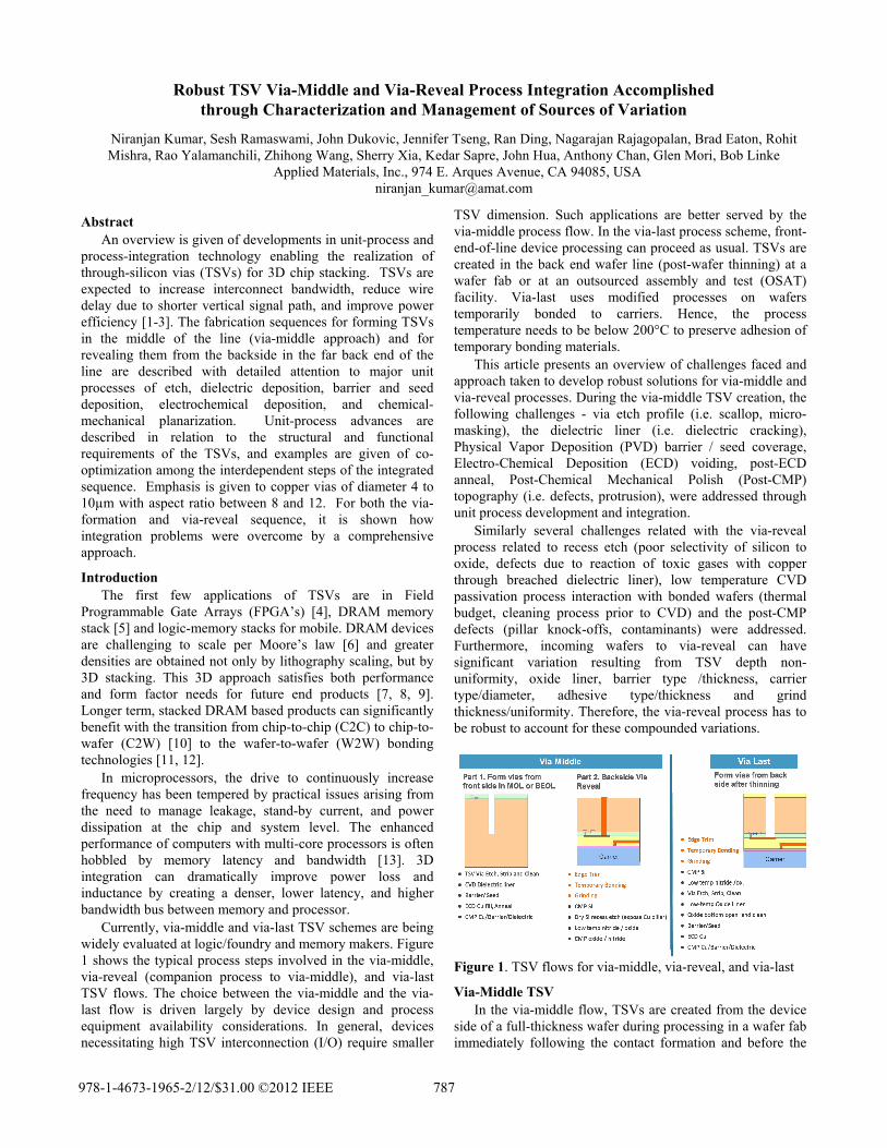
Figure 3 shows high step-coverage (>50%) performance of CVD oxide liner in 4x44m and 10x60m TSVs. Sufficient oxide liner thickness at TSV bottom is critical to protect Cu TSVs from reactive gases exposure during the via-reveal dry recess etch process (backside process). Superior electrical performance (low capacitance, low leakage) requires high quality film with improved properties. Minimum oxide liner thickness inside the TSV can be tuned in the range from 0.2m to 1m depending on the device requirement. Furthermore, the oxide liner must have a high breakdown voltage, low leakage current and strong adhesion
788
to silicon. Post-etch clean and improved liner films have shown robustness against previously seen failures at the TSV bottom corner and the top corners. Previously published modeling results [15] have shown impact of liner intrinsic properties and cohesive strength on TSV coupling capacitance, RC delay, TSV reliability.
Figure 3. Sidewall oxide conformality and scaling in via-middle TSVs
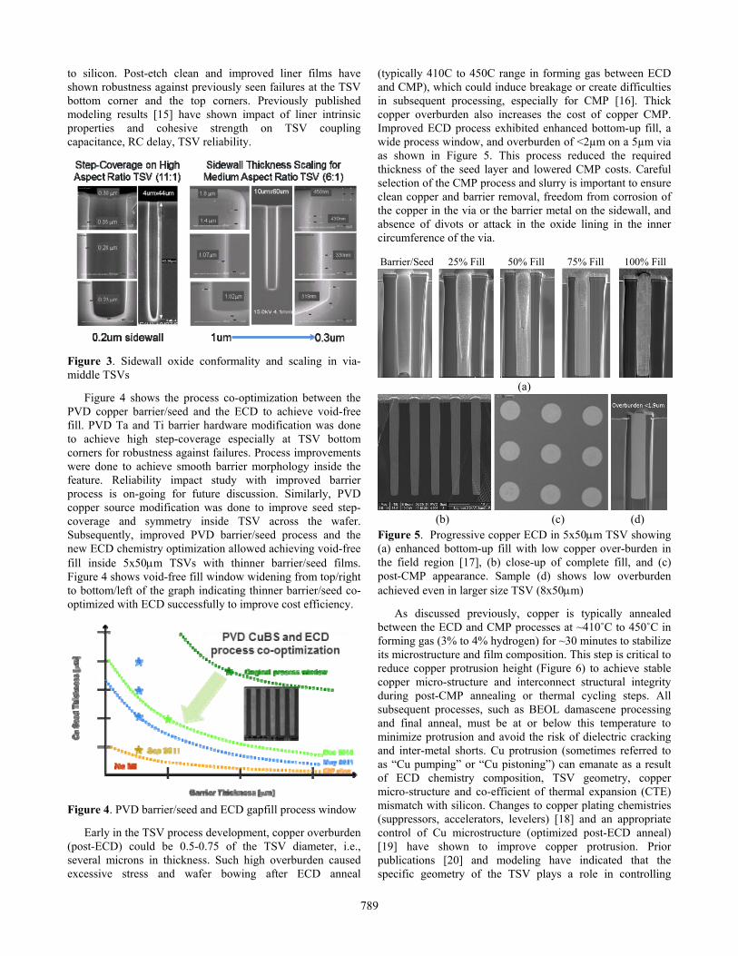
Figure 4 shows the process co-optimization between the PVD copper barrier/seed and the ECD to achieve void-free fill. PVD Ta and Ti barrier hardware modification was done to achieve high step-coverage especially at TSV bottom corners for robustness against failures. Process improvements were done to achieve smooth barrier morphology inside the feature. Reliability impact study with improved barrier process is on-going for future discussion. Similarly, PVD copper source modification was done to improve seed step-coverage and symmetry inside TSV across the wafer. Subsequently, improved PVD barrier/seed process and the new ECD chemistry optimization allowed achieving void-free fill inside 5x50m TSVs with thinner barrier/seed films. Figure 4 shows void-free fill window widening from top/right to bottom/left of the graph indicating thinner barrier/seed co-optimized with ECD successfully to improve cost efficiency.
Figure 4. PVD barrier/seed and ECD gapfill process window
Early in the TSV process development, copper overburden (post-ECD) could be 0.5-0.75 of the TSV diameter, i.e., several microns in thickness. Such high overburden caused excessive stress and wafer bowing after ECD anneal
(typically 410C to 450C range in forming gas between ECD and CMP), which could induce breakage or create difficulties in subsequent processing, especially for CMP [16]. Thick copper overburden also increases the cost of copper CMP. Improved ECD process exhibited enhanced bottom-up fill, a wide process window, and overburden of <2µm on a 5µm via as shown in Figure 5. This process reduced the required thickness of the seed layer and lowered CMP costs. Careful selection of the CMP process and slurry is important to ensure clean copper and barrier removal, freedom from corrosion of the copper in the via or the barrier metal on the sidewall, and absence of divots or attack in the oxide lining in the inner circumference of the via.
(a)
(b) (c) (d) Figure 5. Progressive copper ECD in 5x50m TSV showing (a) enhanced bottom-up fill with low copper over-burden in the field region [17], (b) close-up of complete fill, and (c) post-CMP appearance. Sample (d) shows low overburden achieved even in larger size TSV (8x50m)
As discussed previously, copper is typically annealed between the ECD and CMP processes at ~410˚C to 450˚C in forming gas (3% to 4% hydrogen) for ~30 minutes to stabilize its microstructure and film composition. This step is critical to reduce copper protrusion height (Figure 6) to achieve stable copper micro-structure and interconnect structural integrity during post-CMP annealing or thermal cycling steps. All subsequent processes, such as BEOL damascene processing and final anneal, must be at or below this temperature to minimize protrusion and avoid the risk of dielectric cracking and inter-metal shorts. Cu protrusion (sometimes referred to as “Cu pumping” or “Cu pistoning”) can emanate as a result of ECD chemistry composition, TSV geometry, copper micro-structure and co-efficient of thermal expansion (CTE) mismatch with silicon. Changes to copper plating chemistries (suppressors, accelerators, levelers) [18] and an appropriate control of Cu microstructure (optimized post-ECD anneal) [19] have shown to improve copper protrusion. Prior publications [20] and modeling have indicated that the specific geometry of the TSV plays a role in controlling
Barrier/Seed 25% Fill 50% Fill 75% Fill 100% Fill
789

pistoning. Characterization of thermo-mechanical stress and reliability issues of larger interposer TSVs (50x150m, 50x210m and 50x315m) have shown that annealing at 400C for 1-2 hours may be sufficient to stabilize Cu TSVs prior to subsequent processing [21]. This study has also shown that increased copper protrusion occurs in larger size TSVs due to the ability to grow larger grains. This comes to an advantage for mainstream smaller via-middle TSVs (4-10m diameter, 40x100m deep) where the protrusion can be controlled to acceptable limit with anneal times near 30 minutes as shown in Figure 6 below.
Figure 6. Post-ECD anneal is critical to achieve low copper protrusion and stable micro-structure. Left top/bottom images (no anneal after ECD, anneal after CMP), show high Cu protrusion post-CMP anneal. Right top/bottom images (anneal after ECD, anneal after CMP), show low copper protrusion as stable micro-structure is achieved after ECD anneal resulting in only slight copper protrusion (<500Å) after CMP anneal.
Via-Reveal Sequence TSV via-reveal, a necessary part of the via-middle TSV
flow, and its dependence on developments in thin-wafer support systems have been a recent focus in the industry. The via-reveal sequence of 10x60m TSV is presented to demonstrate technology readiness. The backside grind and silicon CMP stops short of the TSV as shown in Figure 7, which remains encased within the thinned silicon wafer to ensure that no copper becomes exposed. Then dry etching is done to recess the silicon and leave TSV pillars standing to heights of 2m to 6m, with desired pillar height variation below 1-2m across the wafer, depending on the dielectric of subsequent Re-Distribution Layer (RDL) and bump process. The best dielectric choice may vary depending on the specific application requirements, such as planarity requirements or high frequency operation [21]. Inorganic, low temperature chemical vapor deposition (CVD) oxide and nitride are preferred to organic dielectrics. CVD processes can be adjusted to ensure easier integration with a variety of temporary bonding adhesives. Subsequently, dielectric CMP is done to expose Cu with smooth dielectric insulation between TSVs followed by RDL/bump processing.
Figure 7. TSV via-reveal (<200˚C process) sequence leading to final 3D IC stacking using Cu pillars or micro-bumps
Figure 8. TSV via-reveal improved unit process solutions characterized within an integrated framework
A major challenge of the via-reveal process lies with wafer handoffs in the supply chain, where the packaging house is responsible for via-reveal with no control on via-middle processing done at the foundry. As a result, the
~1500A
Pos
t-C
MP
A
nnea
l (S
EM
Vis
ion)
Pos
t-C
MP
A
nnea
l (P
rofil
omet
ry)
Protrusion ~1500Å Protrusion <500Å
No Post-ECD Anneal Post-ECD Anneal (450C/30min/Forming Gas)
790

incoming wafers to via reveal can have significant compounded variation from TSV depth non-uniformity, oxide liner, barrier type /thickness, carrier type/diameter, adhesive type/thickness and grind thickness/uniformity. The via-reveal process has to be robust enough to handle these compounded variations. As shown in Figure 8, improved unit processes (Etch/CVD/CMP) within an integrated framework and a unique measurement and feed-forward system was used to develop a via-reveal process that is robust with respect to compounded variation of incoming wafers.
Silicon CMP after grind is used to achieve a uniform thickness profile and smooth surface. CMP polish heads with zone-tuning capability play a pivotal role in reducing the total thickness variation (TTV) across the wafer as shown in Figure 9. A special end point system is being developed to enable the integration which reduces overall via-reveal cost of ownership. Advanced post-CMP clean reduces post-grind defects and prepares thinned device wafers for subsequent processes. This ensures robust adhesion between the silicon and dielectric interface.
(a)
(b)
Figure 9. (a) Varying within-wafer (WIW) silicon thickness profiles achievable with CMP polish heads zone tuning i.e. Tunable profile-1 (not-optimized) to profile-2/-3 (optimized). (b) Incoming wafers can have significant wafer-to-wafer (WTW) thickness profile variation. Special endpoint is used to improve the post-CMP WTW profile. (Note: Modulation seen on pre-CMP/ post-CMP silicon surfaces are caused by underlying topography)
Figure 10. Left top/bottom images show defects (copper etch byproduct) with un-optimized etch process. Right top/bottom images show no defect and intact oxide liner, PVD barrier and / or passivation films, when exposed to reactive gases during optimized etch process
Figure 11. Uniform via-reveal height (~1.4m) across wafer achieved by using unique predictive TTV control etch process while oxide liner intact on TSV (10x60m)
After CMP, highly selective silicon recess etch is done to expose the vias without damaging the liner oxide encasing it. Loss of selectivity, poor incoming oxide or barrier, can cause irreparable defects on completed wafers as shown in Figure 10. Improved etch selectivity achieved clean, defect free via-reveal while ensuring oxide liner and barrier integrity during exposure to reactive gases. A unique predictive TTV control
791
(recipe tuning) is developed to improve WIW TTV variation as shown in figure 11. This allows reduced pillar height variation across wafer thereby improving process robustness and cost efficiency.
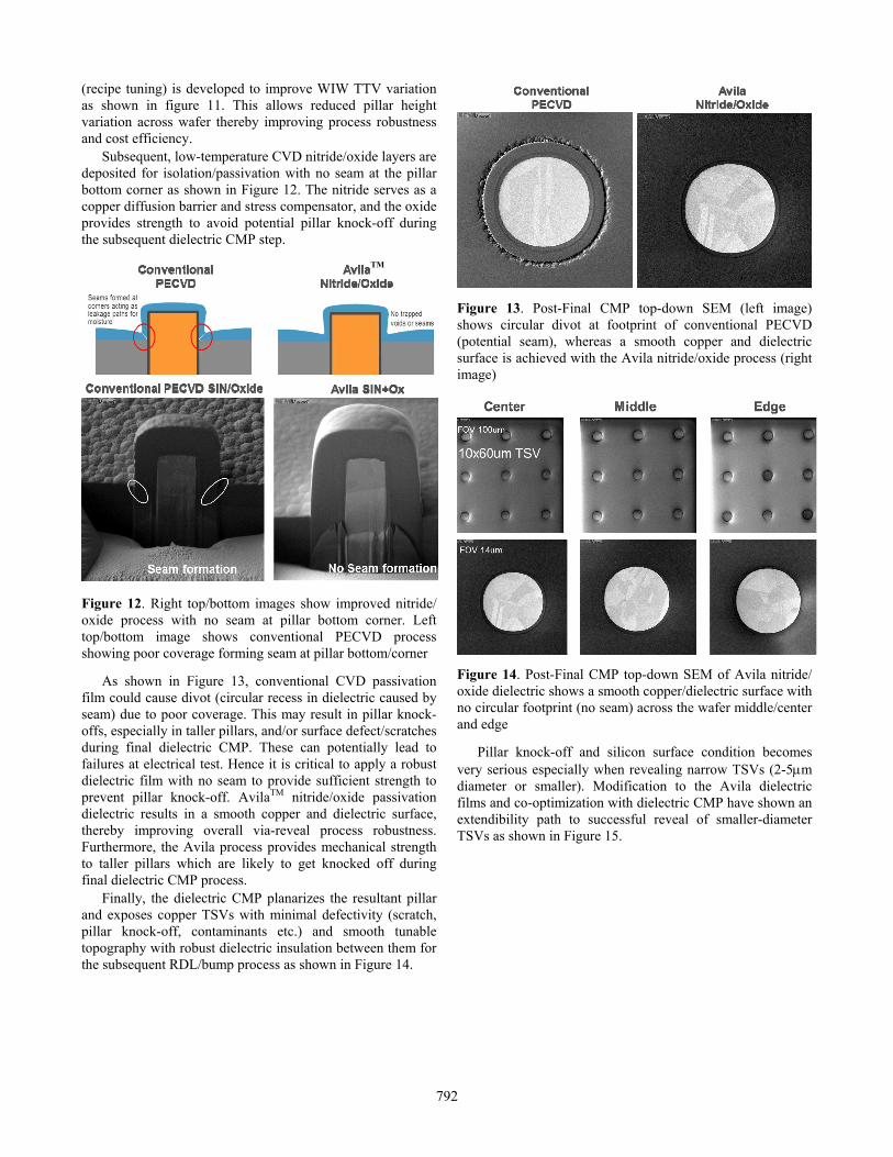
Subsequent, low-temperature CVD nitride/oxide layers are deposited for isolation/passivation with no seam at the pillar bottom corner as shown in Figure 12. The nitride serves as a copper diffusion barrier and stress compensator, and the oxide provides strength to avoid potential pillar knock-off during the subsequent dielectric CMP step.
Figure 12. Right top/bottom images show improved nitride/ oxide process with no seam at pillar bottom corner. Left top/bottom image shows conventional PECVD process showing poor coverage forming seam at pillar bottom/corner
As shown in Figure 13, conventional CVD passivation film could cause divot (circular recess in dielectric caused by seam) due to poor coverage. This may result in pillar knock-offs, especially in taller pillars, and/or surface defect/scratches during final dielectric CMP. These can potentially lead to failures at electrical test. Hence it is critical to apply a robust dielectric film with no seam to provide sufficient strength to prevent pillar knock-off. AvilaTM nitride/oxide passivation dielectric results in a smooth copper and dielectric surface, thereby improving overall via-reveal process robustness. Furthermore, the Avila process provides mechanical strength to taller pillars which are likely to get knocked off during final dielectric CMP process.
Finally, the dielectric CMP planarizes the resultant pillar and exposes copper TSVs with minimal defectivity (scratch, pillar knock-off, contaminants etc.) and smooth tunable topography with robust dielectric insulation between them for the subsequent RDL/bump process as shown in Figure 14.
Figure 13. Post-Final CMP top-down SEM (left image) shows circular divot at footprint of conventional PECVD (potential seam), whereas a smooth copper and dielectric surface is achieved with the Avila nitride/oxide process (right image)
Figure 14. Post-Final CMP top-down SEM of Avila nitride/ oxide dielectric shows a smooth copper/dielectric surface with no circular footprint (no seam) across the wafer middle/center and edge
Pillar knock-off and silicon surface condition becomes very serious especially when revealing narrow TSVs (2-5m diameter or smaller). Modification to the Avila dielectric films and co-optimization with dielectric CMP have shown an extendibility path to successful reveal of smaller-diameter TSVs as shown in Figure 15.
TM
792
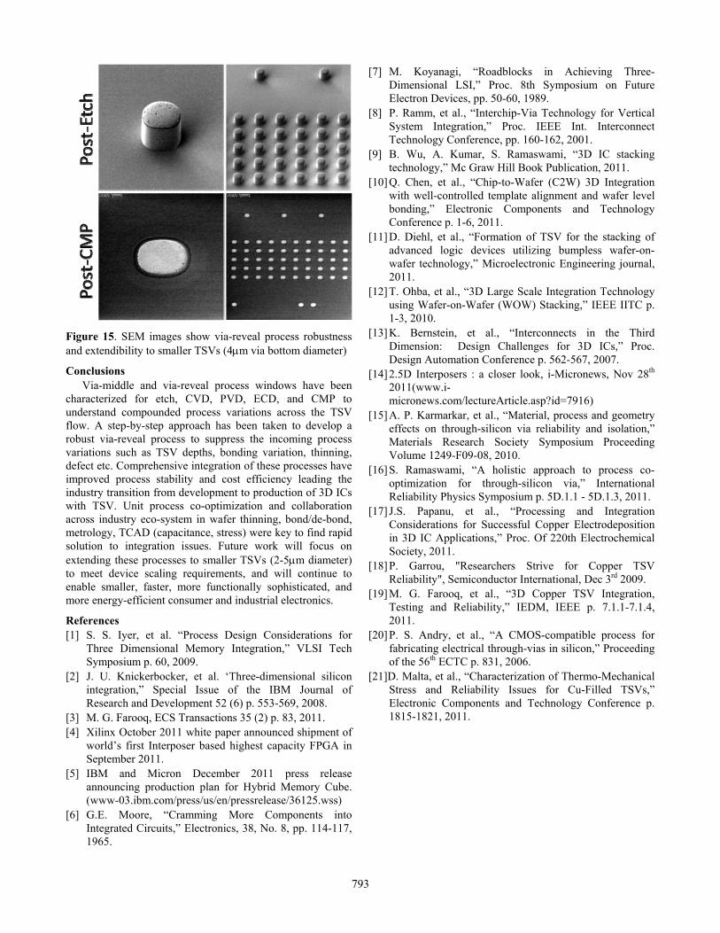
Figure 15. SEM images show via-reveal process robustness and extendibility to smaller TSVs (4m via bottom diameter)
Conclusions Via-middle and via-reveal process windows have been
characterized for etch, CVD, PVD, ECD, and CMP to understand compounded process variations across the TSV flow. A step-by-step approach has been taken to develop a robust via-reveal process to suppress the incoming process variations such as TSV depths, bonding variation, thinning, defect etc. Comprehensive integration of these processes have improved process stability and cost efficiency leading the industry transition from development to production of 3D ICs with TSV. Unit process co-optimization and collaboration across industry eco-system in wafer thinning, bond/de-bond, metrology, TCAD (capacitance, stress) were key to find rapid solution to integration issues. Future work will focus on extending these processes to smaller TSVs (2-5m diameter) to meet device scaling requirements, and will continue to enable smaller, faster, more functionally sophisticated, and more energy-efficient consumer and industrial electronics.
References [1] S. S. Iyer, et al. “Process Design Considerations for
Three Dimensional Memory Integration,” VLSI Tech Symposium p. 60, 2009.
[2] J. U. Knickerbocker, et al. ‘Three-dimensional silicon integration,” Special Issue of the IBM Journal of Research and Development 52 (6) p. 553-569, 2008.
[3] M. G. Farooq, ECS Transactions 35 (2) p. 83, 2011. [4] Xilinx October 2011 white paper announced shipment of
world’s first Interposer based highest capacity FPGA in September 2011.
[5] IBM and Micron December 2011 press release announcing production plan for Hybrid Memory Cube. (www-03.ibm.com/press/us/en/pressrelease/36125.wss)
[6] G.E. Moore, “Cramming More Components into Integrated Circuits,” Electronics, 38, No. 8, pp. 114-117, 1965.
[7] M. Koyanagi, “Roadblocks in Achieving Three-Dimensional LSI,” Proc. 8th Symposium on Future Electron Devices, pp. 50-60, 1989.
[8] P. Ramm, et al., “Interchip-Via Technology for Vertical System Integration,” Proc. IEEE Int. Interconnect Technology Conference, pp. 160-162, 2001.
[9] B. Wu, A. Kumar, S. Ramaswami, “3D IC stacking technology,” Mc Graw Hill Book Publication, 2011.
[10] Q. Chen, et al., “Chip-to-Wafer (C2W) 3D Integration with well-controlled template alignment and wafer level bonding,” Electronic Components and Technology Conference p. 1-6, 2011.
[11] D. Diehl, et al., “Formation of TSV for the stacking of advanced logic devices utilizing bumpless wafer-on-wafer technology,” Microelectronic Engineering journal, 2011.
[12] T. Ohba, et al., “3D Large Scale Integration Technology using Wafer-on-Wafer (WOW) Stacking,” IEEE IITC p. 1-3, 2010.
[13] K. Bernstein, et al., “Interconnects in the Third Dimension: Design Challenges for 3D ICs,” Proc. Design Automation Conference p. 562-567, 2007.
[14] 2.5D Interposers : a closer look, i-Micronews, Nov 28th 2011(www.i-micronews.com/lectureArticle.asp?id=7916)
[15] A. P. Karmarkar, et al., “Material, process and geometry effects on through-silicon via reliability and isolation,” Materials Research Society Symposium Proceeding Volume 1249-F09-08, 2010.
[16] S. Ramaswami, “A holistic approach to process co-optimization for through-silicon via,” International Reliability Physics Symposium p. 5D.1.1 - 5D.1.3, 2011.
[17] J.S. Papanu, et al., “Processing and Integration Considerations for Successful Copper Electrodeposition in 3D IC Applications,” Proc. Of 220th Electrochemical Society, 2011.
[18] P. Garrou, "Researchers Strive for Copper TSV Reliability", Semiconductor International, Dec 3rd 2009.
[19] M. G. Farooq, et al., “3D Copper TSV Integration, Testing and Reliability,” IEDM, IEEE p. 7.1.1-7.1.4, 2011.
[20] P. S. Andry, et al., “A CMOS-compatible process for fabricating electrical through-vias in silicon,” Proceeding of the 56th ECTC p. 831, 2006.
[21]D. Malta, et al., “Characterization of Thermo-Mechanical Stress and Reliability Issues for Cu-Filled TSVs,” Electronic Components and Technology Conference p. 1815-1821, 2011.
793