
ROBUST CAPACITIVE MEMS ULTRASONICS TRANSDUCERS
4
ROBUST CAPACITIVE MEMS ULTRASONICS TRANSDUCERS FOR LIQUID IMMERSION D.W. Greve and J.J. Neumann Department of Electrical and Computer Engineering, Carnegie Mellon University, Pittsburgh, PA, USA I.J. Oppenheim Department of Civil and Environmental Engineering, Carnegie Mellon University, Pittsburgh, PA, USA S.P. Pessiki and D. Ozevin Dept. of Civil and Environmental Engineering, Lehigh University, Bethlehem, PA, USA Abstract - Capacitive diaphragm MEMS ultrasonic transducers are of great interest because they offer wide bandwidth and ready integration into arrays. However, fragility of these transducers is a significant barrier to their application. In this talk, we report on robust transducers which have been fabricated using the MUMPS process. The transducer design has been optimized to minimize stray capacitance between the output node and the substrate. We report the use of a protective silicone layer which protects the transducers from liquid exposure and, to a degree, from mechani- cal damage. The silicone layer has been applied with high trans- ducer yield without the need for prior closure of the etch holes, and coated transducers survive extended immersion in water. The thickness of the silicone layer must be carefully controlled, how- ever, in order to prevent pulse distortion. I. INTRODUCTION MEMS ultrasonic transducers (sometimes termed cMUTs, for capacitive MEMS Ultrasonic Transduc- ers), have been studied by several research groups [1,2,3,4,5,6] both for liquid immersion applications [1,2,3,4] and also in contact with solid media [5,6]. In many of these applications fragility of the transducers is an important issue. Here, we will report on the use of a thin silicone coating to provide acoustic cou- pling, electrical insulation, and a degree of mechani- cal protection. II. TRANSDUCER FABRICATION Transducers used in this work were fabricated using the MUMPS multi-user MEMS process on 1 cm 2 chips using the POLY0 and POLY1 layers. Each transducer consisted of an array of hexagonal units and the upper electrode was released by etching the sacrificial SiO 2 layer through 5 µm square etch holes. An optical micrograph of one of the transducer arrays is shown in Fig. 1. Fig. 1. Optical micrograph of transducer (design B). A range of different transducer designs were studied as indicated in Table I. Transducer design A was the same design previously used to explore coupling to a solid medium [5] and had a POLY0-POLY1 gap of 2.0 µm and relatively high parasitic capacitance be- tween the POLY1 electrode and the substrate. In con- trast designs B-F used the DIMPLE mask level to reduce the electrode gap to 1.25 µm and in addition the capacitance between the POLY1 electrode and the substrate were reduced by an improved design for the diaphragm supports. These two changes have the ef- fect of increasing the signal levels observed off-chip. label edge [µm] number C d [pF] C stray [pF] f r [kHz] A 37 180 2.9 150 3470 B 137 95 10.9 80.6 1060 C 157 81 12.2 70.3 812 D1 177 68 13.1 82.4 658 D2 177 68 13.1 69.4 662 E1 207 53 13.9 80.0 482 E2 207 53 13.9 68.9 483 F1 242 36 12.9 74.3 359 F2 242 36 12.9 60.3 366 Table I. Characteristics of transducers used in this work. C d is the diaphragm capacitance calaculated from the lay- out and C stray is the measured stray capacitance.
Transcript of ROBUST CAPACITIVE MEMS ULTRASONICS TRANSDUCERS
ROBUST CAPACITIVE MEMS ULTRASONICS TRANSDUCERS FOR LIQUID IMMERSION
D.W. Greve and J.J. Neumann Department of Electrical and Computer Engineering, Carnegie Mellon University, Pittsburgh, PA, USA
I.J. Oppenheim Department of Civil and Environmental Engineering, Carnegie Mellon University, Pittsburgh, PA, USA
S.P. Pessiki and D. Ozevin Dept. of Civil and Environmental Engineering, Lehigh University, Bethlehem, PA, USA
Abstract - Capacitive diaphragm MEMS ultrasonic transducers are of great interest because they offer wide bandwidth and ready integration into arrays. However, fragility of these transducers is a significant barrier to their application. In this talk, we report on robust transducers which have been fabricated using the MUMPS process. The transducer design has been optimized to minimize stray capacitance between the output node and the substrate. We report the use of a protective silicone layer which protects the transducers from liquid exposure and, to a degree, from mechani-cal damage. The silicone layer has been applied with high trans-ducer yield without the need for prior closure of the etch holes, and coated transducers survive extended immersion in water. The thickness of the silicone layer must be carefully controlled, how-ever, in order to prevent pulse distortion.
I. INTRODUCTION
MEMS ultrasonic transducers (sometimes termed cMUTs, for capacitive MEMS Ultrasonic Transduc-ers), have been studied by several research groups [1,2,3,4,5,6] both for liquid immersion applications [1,2,3,4] and also in contact with solid media [5,6]. In many of these applications fragility of the transducers is an important issue. Here, we will report on the use of a thin silicone coating to provide acoustic cou-pling, electrical insulation, and a degree of mechani-cal protection.
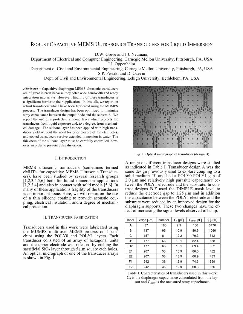
II. TRANSDUCER FABRICATION Transducers used in this work were fabricated using the MUMPS multi-user MEMS process on 1 cm2 chips using the POLY0 and POLY1 layers. Each transducer consisted of an array of hexagonal units and the upper electrode was released by etching the sacrificial SiO2 layer through 5 µm square etch holes. An optical micrograph of one of the transducer arrays is shown in Fig. 1.
Fig. 1. Optical micrograph of transducer (design B).
A range of different transducer designs were studied as indicated in Table I. Transducer design A was the same design previously used to explore coupling to a solid medium [5] and had a POLY0-POLY1 gap of 2.0 µm and relatively high parasitic capacitance be-tween the POLY1 electrode and the substrate. In con-trast designs B-F used the DIMPLE mask level to reduce the electrode gap to 1.25 µm and in addition the capacitance between the POLY1 electrode and the substrate were reduced by an improved design for the diaphragm supports. These two changes have the ef-fect of increasing the signal levels observed off-chip.
label edge [µm] number Cd [pF] Cstray [pF] fr [kHz] A 37 180 2.9 150 3470 B 137 95 10.9 80.6 1060 C 157 81 12.2 70.3 812
D1 177 68 13.1 82.4 658 D2 177 68 13.1 69.4 662 E1 207 53 13.9 80.0 482 E2 207 53 13.9 68.9 483 F1 242 36 12.9 74.3 359 F2 242 36 12.9 60.3 366
Table I. Characteristics of transducers used in this work. Cd is the diaphragm capacitance calaculated from the lay-
out and Cstray is the measured stray capacitance.
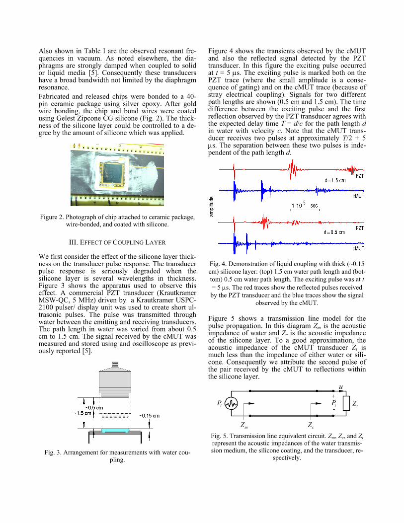
Also shown in Table I are the observed resonant fre-quencies in vacuum. As noted elsewhere, the dia-phragms are strongly damped when coupled to solid or liquid media [5]. Consequently these transducers have a broad bandwidth not limited by the diaphragm resonance. Fabricated and released chips were bonded to a 40-pin ceramic package using silver epoxy. After gold wire bonding, the chip and bond wires were coated using Gelest Zipcone CG silicone (Fig. 2). The thick-ness of the silicone layer could be controlled to a de-gree by the amount of silicone which was applied.
Figure 2. Photograph of chip attached to ceramic package,
wire-bonded, and coated with silicone.
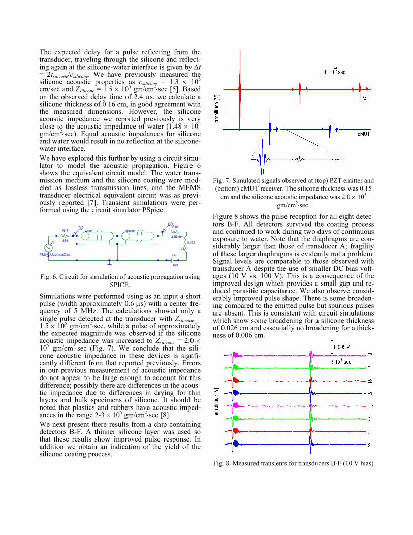
III. EFFECT OF COUPLING LAYER We first consider the effect of the silicone layer thick-ness on the transducer pulse response. The transducer pulse response is seriously degraded when the silicone layer is several wavelengths in thickness. Figure 3 shows the apparatus used to observe this effect. A commercial PZT transducer (Krautkramer MSW-QC, 5 MHz) driven by a Krautkramer USPC-2100 pulser/ display unit was used to create short ul-trasonic pulses. The pulse was transmitted through water between the emitting and receiving transducers. The path length in water was varied from about 0.5 cm to 1.5 cm. The signal received by the cMUT was measured and stored using and oscilloscope as previ-ously reported [5].
Fig. 3. Arrangement for measurements with water cou-
pling.
Figure 4 shows the transients observed by the cMUT and also the reflected signal detected by the PZT transducer. In this figure the exciting pulse occurred at t = 5 µs. The exciting pulse is marked both on the PZT trace (where the small amplitude is a conse-quence of gating) and on the cMUT trace (because of stray electrical coupling). Signals for two different path lengths are shown (0.5 cm and 1.5 cm). The time difference between the exciting pulse and the first reflection observed by the PZT transducer agrees with the expected delay time T = d/c for the path length d in water with velocity c. Note that the cMUT trans-ducer receives two pulses at approximately T/2 + 5 µs. The separation between these two pulses is inde-pendent of the path length d.
Fig. 4. Demonstration of liquid coupling with thick (~0.15 cm) silicone layer: (top) 1.5 cm water path length and (bot-tom) 0.5 cm water path length. The exciting pulse was at t = 5 µs. The red traces show the reflected pulses received by the PZT transducer and the blue traces show the signal
observed by the cMUT. Figure 5 shows a transmission line model for the pulse propagation. In this diagram Zm is the acoustic impedance of water and Zc is the acoustic impedance of the silicone layer. To a good approximation, the acoustic impedance of the cMUT transducer Zt is much less than the impedance of either water or sili-cone. Consequently we attribute the second pulse of the pair received by the cMUT to reflections within the silicone layer.
u+
-mZ cZ
iP tP tZ
Fig. 5. Transmission line equivalent circuit. Zm, Zc, and Zt represent the acoustic impedances of the water transmis-sion medium, the silicone coating, and the transducer, re-
spectively.
The expected delay for a pulse reflecting from the transducer, traveling through the silicone and reflect-ing again at the silicone-water interface is given by ∆t = 2tsilicone/csilicone. We have previously measured the silicone acoustic properties as csilicone = 1.3 × 105 cm/sec and Zsilicone = 1.5 × 10⁵ gm/cm2⋅sec [5]. Based on the observed delay time of 2.4 µs, we calculate a silicone thickness of 0.16 cm, in good agreement with the measured dimensions. However, the silicone acoustic impedance we reported previously is very close to the acoustic impedance of water (1.48 × 10⁵ gm/cm2⋅sec). Equal acoustic impedances for silicone and water would result in no reflection at the silicone-water interface. We have explored this further by using a circuit simu-lator to model the acoustic propagation. Figure 6 shows the equivalent circuit model. The water trans-mission medium and the silicone coating were mod-eled as lossless transmission lines, and the MEMS transducer electrical equivalent circuit was as previ-ously reported [7]. Transient simulations were per-formed using the circuit simulator PSpice.
3E4
R13 water silicone
+
-FILE=C:\cktsim\dat2.dat
V9
16pF
C6
3.15 ohm
R10
0.132
L4
VV
Fig. 6. Circuit for simulation of acoustic propagation using
SPICE.
Simulations were performed using as an input a short pulse (width approximately 0.6 µs) with a center fre-quency of 5 MHz. The calculations showed only a single pulse detected at the transducer with Zsilicone = 1.5 × 10⁵ gm/cm2⋅sec, while a pulse of approximately the expected magnitude was observed if the silicone acoustic impedance was increased to Zsilicone = 2.0 × 10⁵ gm/cm2⋅sec (Fig. 7). We conclude that the sili-cone acoustic impedance in these devices is signfi-cantly different from that reported previously. Errors in our previous measurement of acoustic impedance do not appear to be large enough to account for this difference; possibly there are differences in the acous-tic impedance due to differences in drying for thin layers and bulk specimens of silicone. It should be noted that plastics and rubbers have acoustic imped-ances in the range 2-3 × 10⁵ gm/cm2⋅sec [8]. We next present there results from a chip containing detectors B-F. A thinner silicone layer was used so that these results show improved pulse response. In addition we obtain an indication of the yield of the silicone coating process.
Fig. 7. Simulated signals observed at (top) PZT emitter and (bottom) cMUT receiver. The silicone thickness was 0.15
cm and the silicone acoustic impedance was 2.0 × 10⁵ gm/cm2⋅sec.
Figure 8 shows the pulse reception for all eight detec-tors B-F. All detectors survived the coating process and continued to work during two days of continuous exposure to water. Note that the diaphragms are con-siderably larger than those of transducer A; fragility of these larger diaphragms is evidently not a problem. Signal levels are comparable to those observed with transducer A despite the use of smaller DC bias volt-ages (10 V vs. 100 V). This is a consequence of the improved design which provides a small gap and re-duced parasitic capacitance. We also observe consid-erably improved pulse shape. There is some broaden-ing compared to the emitted pulse but spurious pulses are absent. This is consistent with circuit simulations which show some broadening for a silicone thickness of 0.026 cm and essentially no broadening for a thick-ness of 0.006 cm.
Fig. 8. Measured transients for transducers B-F (10 V bias)
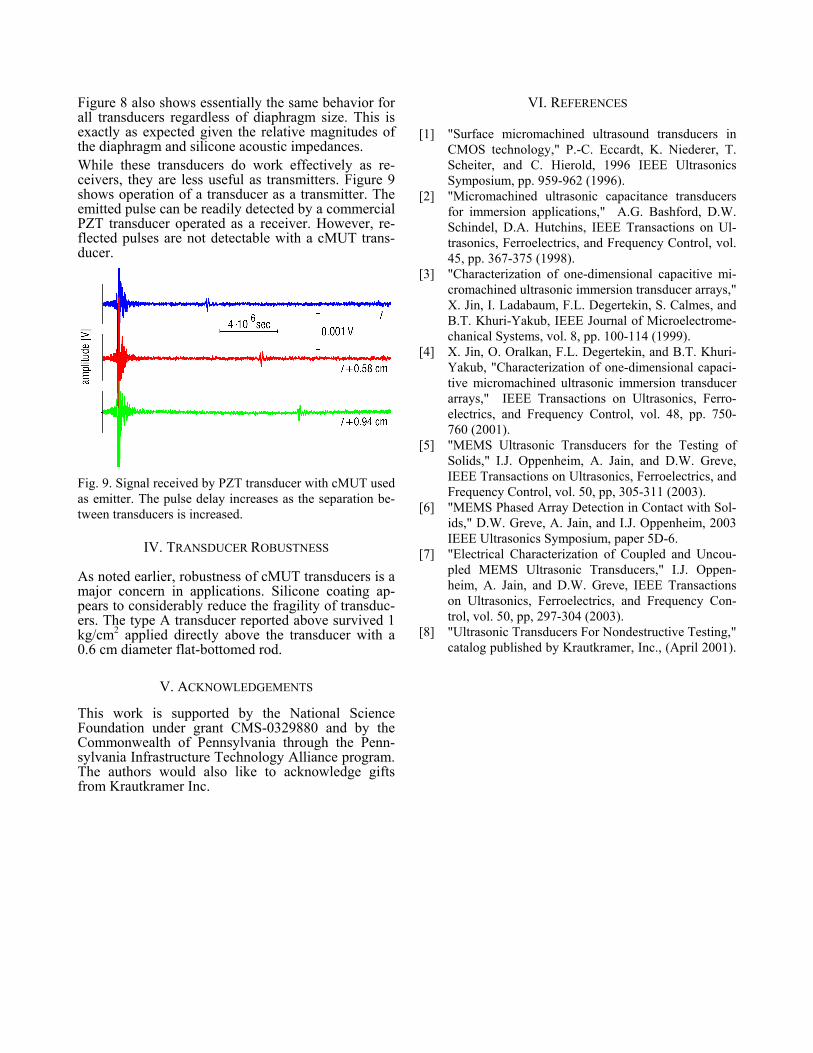
Figure 8 also shows essentially the same behavior for all transducers regardless of diaphragm size. This is exactly as expected given the relative magnitudes of the diaphragm and silicone acoustic impedances. While these transducers do work effectively as re-ceivers, they are less useful as transmitters. Figure 9 shows operation of a transducer as a transmitter. The emitted pulse can be readily detected by a commercial PZT transducer operated as a receiver. However, re-flected pulses are not detectable with a cMUT trans-ducer.
Fig. 9. Signal received by PZT transducer with cMUT used as emitter. The pulse delay increases as the separation be-tween transducers is increased.
IV. TRANSDUCER ROBUSTNESS
As noted earlier, robustness of cMUT transducers is a major concern in applications. Silicone coating ap-pears to considerably reduce the fragility of transduc-ers. The type A transducer reported above survived 1 kg/cm2 applied directly above the transducer with a 0.6 cm diameter flat-bottomed rod.
V. ACKNOWLEDGEMENTS This work is supported by the National Science Foundation under grant CMS-0329880 and by the Commonwealth of Pennsylvania through the Penn-sylvania Infrastructure Technology Alliance program. The authors would also like to acknowledge gifts from Krautkramer Inc.
VI. REFERENCES [1] "Surface micromachined ultrasound transducers in
CMOS technology," P.-C. Eccardt, K. Niederer, T. Scheiter, and C. Hierold, 1996 IEEE Ultrasonics Symposium, pp. 959-962 (1996).
[2] "Micromachined ultrasonic capacitance transducers for immersion applications," A.G. Bashford, D.W. Schindel, D.A. Hutchins, IEEE Transactions on Ul-trasonics, Ferroelectrics, and Frequency Control, vol. 45, pp. 367-375 (1998).
[3] "Characterization of one-dimensional capacitive mi-cromachined ultrasonic immersion transducer arrays," X. Jin, I. Ladabaum, F.L. Degertekin, S. Calmes, and B.T. Khuri-Yakub, IEEE Journal of Microelectrome-chanical Systems, vol. 8, pp. 100-114 (1999).
[4] X. Jin, O. Oralkan, F.L. Degertekin, and B.T. Khuri-Yakub, "Characterization of one-dimensional capaci-tive micromachined ultrasonic immersion transducer arrays," IEEE Transactions on Ultrasonics, Ferro-electrics, and Frequency Control, vol. 48, pp. 750-760 (2001).
[5] "MEMS Ultrasonic Transducers for the Testing of Solids," I.J. Oppenheim, A. Jain, and D.W. Greve, IEEE Transactions on Ultrasonics, Ferroelectrics, and Frequency Control, vol. 50, pp, 305-311 (2003).
[6] "MEMS Phased Array Detection in Contact with Sol-ids," D.W. Greve, A. Jain, and I.J. Oppenheim, 2003 IEEE Ultrasonics Symposium, paper 5D-6.
[7] "Electrical Characterization of Coupled and Uncou-pled MEMS Ultrasonic Transducers," I.J. Oppen-heim, A. Jain, and D.W. Greve, IEEE Transactions on Ultrasonics, Ferroelectrics, and Frequency Con-trol, vol. 50, pp, 297-304 (2003).
[8] "Ultrasonic Transducers For Nondestructive Testing," catalog published by Krautkramer, Inc., (April 2001).


![Surface Micromachined Capacitive Ultrasonic Transducers · coupled ultrasonic inspections motivate the development of air transducers [1]{[5] and the advantages of limited di raction](https://static.fdocuments.in/doc/165x107/5f75b2fed63e901fb755300d/surface-micromachined-capacitive-ultrasonic-transducers-coupled-ultrasonic-inspections.jpg)

![Large Scale Capacitive Skin for Robots - IntechOpen · 2012-10-11 · Large Scale Capacitive Skin for Robots 3 robots Robovie-IIS [10] and CB2 [11]. The transducers were placed individually](https://static.fdocuments.in/doc/165x107/5f11cfedad5441286f78ad51/large-scale-capacitive-skin-for-robots-intechopen-2012-10-11-large-scale-capacitive.jpg)


