RK3288 TRM - Rockchiprockchip.fr/RK3288...
26
RK3288 TRM FuZhou Rockchip Electronics Co.,Ltd. 1626 Chapter 53 Universal Asynchronous Receiver/Transmitter (UART) 53.1 Overview The Universal Asynchronous Receiver/Transmitter (UART) is used for serial communication with a peripheral, modem (data carrier equipment, DCE) or data set. Data is written from a master (CPU) over the APB bus to the UART and it is converted to serial form and transmitted to the destination device. Serial data is also received by the UART and stored for the master (CPU) to read back. UART Controller supports the following features: AMBA APB interface – Allows for easy integration into a Synthesizable Components for AMBA 2 implementation Support interrupt interface to interrupt controller Contain two 64Bytes FIFOs for data receive and transmit Programmable serial data baud rate as calculated by the following: baud rate = (serial clock frequency)/(16×divisor) UART_BB/UART_BT/UART_GPS/UART_EXP support auto flow-control, UART_DBG do not support auto flow-control UART_DBG support IrDA 1.0 SIR mode with up to 115.2 Kbaud data rate UART_BB/UART_BT/UART_GPS/UART_EXP are in peripheral subsystem, UART_DBG is in bus subsystem 53.2 Block Diagram This section provides a description about the functions and behavior under various conditions. The UART Controller comprises with: AMBA APB interface FIFO controllers Register block Modem synchronization block and baud clock generation block Serial receiver and serial transmitter apb interface modem sync register block fifo block baud clock generation serial receiver serial transmitter apb bus baudout_n sout sir_out_n dma_tx_req dma_rx_req dma_tx_ack dma_rx_ack intr dtr_n rts_n cts_n dsr_n sin sir_in_n Fig. 53-1 UART Architecture APB INTERFACE T-chip Only
Transcript of RK3288 TRM - Rockchiprockchip.fr/RK3288...

RK3288 TRM
FuZhou Rockchip Electronics Co.,Ltd. 1626
Chapter 53 Universal Asynchronous Receiver/Transmitter
(UART)
53.1 Overview
The Universal Asynchronous Receiver/Transmitter (UART) is used for serial communication
with a peripheral, modem (data carrier equipment, DCE) or data set. Data is written from a master (CPU) over the APB bus to the UART and it is converted to serial form and transmitted
to the destination device. Serial data is also received by the UART and stored for the master
(CPU) to read back.
UART Controller supports the following features:
AMBA APB interface – Allows for easy integration into a Synthesizable Components for
AMBA 2 implementation Support interrupt interface to interrupt controller
Contain two 64Bytes FIFOs for data receive and transmit
Programmable serial data baud rate as calculated by the following: baud rate = (serial clock frequency)/(16×divisor)
UART_BB/UART_BT/UART_GPS/UART_EXP support auto flow-control, UART_DBG do not
support auto flow-control
UART_DBG support IrDA 1.0 SIR mode with up to 115.2 Kbaud data rate
UART_BB/UART_BT/UART_GPS/UART_EXP are in peripheral subsystem, UART_DBG is in
bus subsystem
53.2 Block Diagram
This section provides a description about the functions and behavior under various conditions. The UART Controller comprises with:
AMBA APB interface
FIFO controllers Register block
Modem synchronization block and baud clock generation block
Serial receiver and serial transmitter
apb
interface
modem
sync
register
block
fifo
block
baud
clock
generation
serial
receiver
serial
transmitter
apb
bus
baudout_n
sout
sir_out_n
dma_tx_req
dma_rx_req
dma_tx_ack
dma_rx_ack
intr
dtr_n
rts_n
cts_n
dsr_n
sin
sir_in_n
Fig. 53-1 UART Architecture
APB INTERFACE
T-chip Only

RK3288 TRM
FuZhou Rockchip Electronics Co.,Ltd. 1627
The host processor accesses data, control, and status information on the UART through the
APB interface. The UART supports APB data bus widths of 8, 16, and 32 bits.
Register block
Be responsible for the main UART functionality including control, status and interrupt
generation.
Modem Synchronization block
Synchronizes the modem input signal.
FIFO block
Be responsible for FIFO control and storage (when using internal RAM) or signaling to control
external RAM (when used).
Baud Clock Generator
Generate the transmitter and receiver baud clock along with the output reference clock signal
(baudout_n).
Serial Transmitter
Converts the parallel data, written to the UART, into serial form and adds all additional bits, as
specified by the control register, for transmission. This makeup of serial data, referred to as a
character can exit the block in two forms, either serial UART format or IrDA 1.0 SIR format.
Serial Receiver
Converts the serial data character (as specified by the control register) received in either the
UART or IrDA 1.0 SIR format to parallel form. Parity error detection, framing error detection
and line break detection is carried out in this block.
53.3 Function description
UART (RS232) Serial Protocol
Because the serial communication is asynchronous, additional bits (start and stop) are added
to the serial data to indicate the beginning and end. An additional parity bit may be added to the serial character. This bit appears after the last data bit and before the stop bit(s) in the
character structure to perform simple error checking on the received data, as shown in Figure.
Fig. 53-2 UART Serial protocol
IrDA 1.0 SIR Protocol
The Infrared Data Association (IrDA) 1.0 Serial Infrared (SIR) mode supports bi-directional
data communications with remote devices using infrared radiation as the transmission
medium. IrDA 1.0 SIR mode specifies a maximum baud rate of 115.2 Kbaud.
Transmitting a single infrared pulse signals a logic zero, while a logic one is represented by not sending a pulse. The width of each pulse is 3/16ths of a normal serial bit time. Data transfers
can only occur in half-duplex fashion when IrDA SIR mode is enabled.
T-chip Only

RK3288 TRM
FuZhou Rockchip Electronics Co.,Ltd. 1628
Fig. 53-3 IrDA 1.0
Baud Clock
The baud rate is controlled by the serial clock (sclk or pclk in a single clock implementation)
and the Divisor Latch Register (DLH and DLL). As the exact number of baud clocks that each bit was transmitted for is known, calculating the mid-point for sampling is not difficult, that is
every 16 baud clocks after the mid point sample of the start bit.
Fig. 53-4 UART baud rate
FIFO Support
1. NONE FIFO MODE
If FIFO support is not selected, then no FIFOs are implemented and only a single receive data byte and transmit data byte can be stored at a time in the RBR and THR.
2. FIFO MODE
The FIFO depth of UART1/UART2/UART3 is 32bytes and the FIFO depth of UART0 is 64bytes. The FIFO mode of all the UART is enabled by register FCR[0].
Interrupts
The following interrupt types can be enabled with the IER register.
Receiver Error
Receiver Data Available
Character Timeout (in FIFO mode only) Transmitter Holding Register Empty at/below threshold (in Programmable THRE Interrupt
mode)
Modem Status
DMA Support
The uart supports DMA signaling with the use of two output signals (dma_tx_req_n and
dma_rx_req_n) to indicate when data is ready to be read or when the transmit FIFO is empty.
The dma_tx_req_n signal is asserted under the following conditions:
When the Transmitter Holding Register is empty in non-FIFO mode.
When the transmitter FIFO is empty in FIFO mode with Programmable THRE interrupt
mode disabled. When the transmitter FIFO is at, or below the programmed threshold with Programmable
THRE interrupt mode enabled.
T-chip Only

RK3288 TRM
FuZhou Rockchip Electronics Co.,Ltd. 1629
The dma_rx_req_n signal is asserted under the following conditions:
When there is a single character available in the Receive Buffer Register in non-FIFO mode.
When the Receiver FIFO is at or above the programmed trigger level in FIFO mode.
Auto Flow Control
The UART can be configured to have a 16750-compatible Auto RTS and Auto CTS serial data
flow control mode available. If FIFOs are not implemented, then this mode cannot be selected.
When Auto Flow Control mode has been selected, it can be enabled with the Modem Control Register (MCR[5]). Following figure shows a block diagram of the Auto Flow Control
functionality.
Fig. 53-5 UART Auto flow control block diagram
Auto RTS – Becomes active when the following occurs:
Auto Flow Control is selected during configuration FIFOs are implemented
RTS (MCR[1] bit and MCR[5]bit are both set)
FIFOs are enabled (FCR[0]) bit is set) SIR mode is disabled (MCR[6] bit is not set)
Fig. 53-6 UART AUTO RTS TIMING
T-chip Only

RK3288 TRM
FuZhou Rockchip Electronics Co.,Ltd. 1630
Auto CTS – becomes active when the following occurs:
Auto Flow Control is selected during configuration FIFOs are implemented
AFCE (MCR[5] bit is set)
FIFOs are enabled through FIFO Control Register FCR[0] bit SIR mode is disabled (MCR[6] bit is not set)
Fig. 53-7 UART AUTO CTS TIMING
53.4 Register Description
This section describes the control/status registers of the design. There are 5 UARTs in RK3288, and each one has its own base address.
53.4.1 Registers Summary
Name Offset Size Reset Value Description
UART_RBR 0x0000 W 0x00000000 Receive Buffer Register
UART_THR 0x0000 W 0x00000000 Transmit Holding Register
UART_DLL 0x0000 W 0x00000000 Divisor Latch (Low)
UART_DLH 0x0004 W 0x00000000 Divisor Latch (High)
UART_IER 0x0004 W 0x00000000 Interrupt Enable Register
UART_IIR 0x0008 W 0x00000001 Interrupt Identification
Register
UART_FCR 0x0008 W 0x00000000 FIFO Control Register
UART_LCR 0x000c W 0x00000000 Line Control Register
UART_MCR 0x0010 W 0x00000000 Modem Control Register
UART_LSR 0x0014 W 0x00000060 Line Status Register
UART_MSR 0x0018 W 0x00000000 Modem Status Register
UART_SCR 0x001c W 0x00000000 Scratchpad Register
UART_SRBR 0x0030~
0x006c W 0x00000000
Shadow Receive Buffer
Register
UART_STHR 0x0030~
0x006c W 0x00000000
Shadow Transmit Holding
Register
UART_FAR 0x0070 W 0x00000000 FIFO Access Register
UART_TFR 0x0074 W 0x00000000 Transmit FIFO Read
UART_RFW 0x0078 W 0x00000000 Receive FIFO Write
UART_USR 0x007c W 0x00000006 UART Status Register
UART_TFL 0x0080 W 0x00000000 Transmit FIFO Level
UART_RFL 0x0084 W 0x00000000 Receive FIFO Level
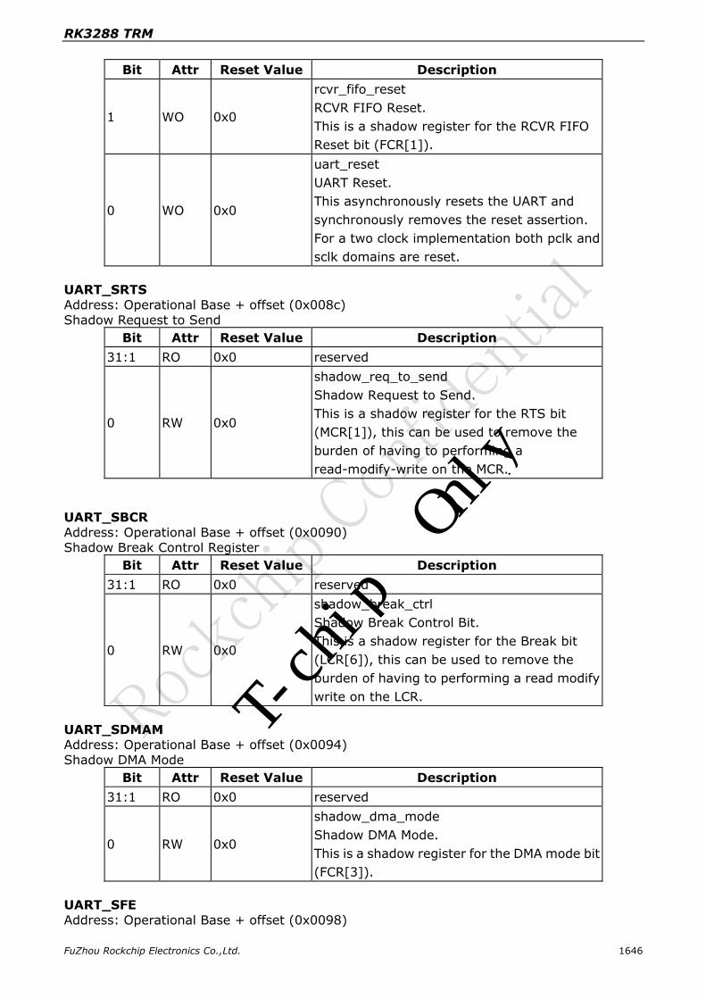
UART_SRR 0x0088 W 0x00000000 Software Reset Register
UART_SRTS 0x008c W 0x00000000 Shadow Request to Send
UART_SBCR 0x0090 W 0x00000000 Shadow Break Control
Register
UART_SDMAM 0x0094 W 0x00000000 Shadow DMA Mode
T-chip Only

RK3288 TRM
FuZhou Rockchip Electronics Co.,Ltd. 1631
Name Offset Size Reset Value Description
UART_SFE 0x0098 W 0x00000000 Shadow FIFO Enable
UART_SRT 0x009c W 0x00000000 Shadow RCVR Trigger
UART_STET 0x00a0 W 0x00000000 Shadow TX Empty Trigger
UART_HTX 0x00a4 W 0x00000000 Halt TX
UART_DMASA 0x00a8 W 0x00000000 DMA Software Acknowledge
UART_CPR 0x00f4 W 0x00000000 Component Parameter
Register
UART_UCV 0x00f8 W 0x3330382a UART Component Version
UART_CTR 0x00fc W 0x44570110 Component Type Register
Notes: Size: B - Byte (8 bits) access, HW - Half WORD (16 bits) access, W -WORD (32 bits) access
53.4.2 Detail Register Description
UART_RBR
Address: Operational Base + offset (0x0000)
Receive Buffer Register
Bit Attr Reset Value Description
31:8 RO 0x0 reserved
7:0 RW 0x00
data_input
Data byte received on the serial input port
(sin) in UART mode, or the serial infrared
input (sir_in) in infrared mode. The data in
this register is valid only if the Data Ready
(DR) bit in the Line Status Register (LCR) is
set.
If in non-FIFO mode (FIFO_MODE == NONE)
or FIFOs are disabled (FCR[0] set to zero), the
data in the RBR must be read before the next
data arrives, otherwise it is overwritten,
resulting in an over-run error.
If in FIFO mode (FIFO_MODE != NONE) and
FIFOs are enabled (FCR[0] set to one), this
register accesses the head of the receive
FIFO. If the receive FIFO is full and this
register is not read before the next data
character arrives, then the data already in the
FIFO is preserved, but any incoming data are
lost and an over-run error occurs.
UART_THR
Address: Operational Base + offset (0x0000) Transmit Holding Register
Bit Attr Reset Value Description
31:8 RO 0x0 reserved
T-chip Only

RK3288 TRM
FuZhou Rockchip Electronics Co.,Ltd. 1632
Bit Attr Reset Value Description
7:0 RW 0x00
data_output
Data to be transmitted on the serial output
port (sout) in UART mode or the serial infrared
output (sir_out_n) in infrared mode. Data
should only be written to the THR when the
THR Empty (THRE) bit (LSR[5]) is set.
If in non-FIFO mode or FIFOs are disabled
(FCR[0] = 0) and THRE is set, writing a single
character to the THR clears the THRE. Any
additional writes to the THR before the THRE
is set again causes the THR data to be
overwritten.
If in FIFO mode and FIFOs are enabled
(FCR[0] = 1) and THRE is set, x number of
characters of data may be written to the THR
before the FIFO is full. The number x
(default=16) is determined by the value of
FIFO Depth that you set during configuration.
Any attempt to write data when the FIFO is full
results in the write data being lost.
UART_DLL Address: Operational Base + offset (0x0000)
Divisor Latch (Low)
Bit Attr Reset Value Description
31:8 RO 0x0 reserved
7:0 RW 0x00
baud_rate_divisor_L
Lower 8-bits of a 16-bit, read/write, Divisor
Latch register that contains the baud rate
divisor for the UART. This register may only be
accessed when the DLAB bit (LCR[7]) is set
and the UART is not busy (USR[0] is zero).
The output baud rate is equal to the serial
clock (sclk) frequency divided by sixteen
times the value of the baud rate divisor, as
follows: baud rate = (serial clock frequency) /
(16 * divisor).
Note that with the Divisor Latch Registers
(DLL and DLH) set to zero, the baud clock is
disabled and no serial communications occur.
Also, once the DLH is set, at least 8 clock
cycles of the slowest UART clock should be
allowed to pass before transmitting or
receiving data.
T-chip Only

RK3288 TRM
FuZhou Rockchip Electronics Co.,Ltd. 1633
UART_DLH
Address: Operational Base + offset (0x0004) Divisor Latch (High)
Bit Attr Reset Value Description
31:8 RO 0x0 reserved
7:0 RW 0x00
baud_rate_divisor_H
Upper 8 bits of a 16-bit, read/write, Divisor
Latch register that contains the baud rate
divisor for the UART.
UART_IER
Address: Operational Base + offset (0x0004)
Interrupt Enable Register
Bit Attr Reset Value Description
31:8 RO 0x0 reserved
7 RW 0x0
prog_thre_int_en
Programmable THRE Interrupt Mode Enable
This is used to enable/disable the generation
of THRE Interrupt.
1’b0: disabled
1’b1: enabled
6:4 RO 0x0 reserved
3 RW 0x0
modem_status_int_en
Enable Modem Status Interrupt.
This is used to enable/disable the generation
of Modem Status Interrupt. This is the fourth
highest priority interrupt.
1’b0: disabled
1’b1: enabled
2 RW 0x0
receive_line_status_int_en
Enable Receiver Line Status Interrupt.
This is used to enable/disable the generation
of Receiver Line Status Interrupt. This is the
highest priority interrupt.
1’b0: disabled
1’b1: enabled
1 RW 0x0
trans_hold_empty_int_en
Enable Transmit Holding Register Empty
Interrupt. T-chip Only

RK3288 TRM
FuZhou Rockchip Electronics Co.,Ltd. 1634
Bit Attr Reset Value Description
0 RW 0x0
receive_data_available_int_en
Enable Received Data Available Interrupt.
This is used to enable/disable the generation
of Received Data Available Interrupt and the
Character Timeout Interrupt (if in FIFO mode
and FIFOs enabled). These are the second
highest priority interrupts.
1’b0: disabled
1’b1: enabled
UART_IIR Address: Operational Base + offset (0x0008)
Interrupt Identification Register
Bit Attr Reset Value Description
31:8 RO 0x0 reserved
7:6 RO 0x0
fifos_en
FIFOs Enabled.
This is used to indicate whether the FIFOs are
enabled or disabled.
2’b00: disabled
2’b11: enabled
5:4 RO 0x0 reserved
3:0 RO 0x1
int_id
Interrupt ID
This indicates the highest priority pending
interrupt which can be one of the following
types:
4’b0000: modem status
4’b0001: no interrupt pending
4’b0010: THR empty
4’b0100: received data available
4’b0110: receiver line status
4’b0111: busy detect
4’b1100: character timeout
UART_FCR
Address: Operational Base + offset (0x0008) FIFO Control Register
Bit Attr Reset Value Description
31:8 RO 0x0 reserved
T-chip Only

RK3288 TRM
FuZhou Rockchip Electronics Co.,Ltd. 1635
Bit Attr Reset Value Description
7:6 WO 0x0
rcvr_trigger
RCVR Trigger.
This is used to select the trigger level in the
receiver FIFO at which the Received Data
Available Interrupt is generated. In auto flow
control mode it is used to determine when the
rts_n signal is de-asserted. It also determines
when the dma_rx_req_n signal is asserted in
certain modes of operation. The following
trigger levels are supported:
2’b00: 1 character in the FIFO
2’b01: FIFO 1/4 full
2’b10: FIFO 1/2 full
2’b11: FIFO 2 less than full
5:4 WO 0x0
tx_empty_trigger
TX Empty Trigger.
This is used to select the empty threshold
level at which the THRE Interrupts are
generated when the mode is active. It also
determines when the dma_tx_req_n signal is
asserted when in certain modes of operation.
The following trigger levels are supported:
2’b00: FIFO empty
2’b01: 2 characters in the FIFO
2’b10: FIFO 1/4 full
2’b11: FIFO 1/2 full
3 WO 0x0
dma_mode
DMA Mode
This determines the DMA signalling mode
used for the dma_tx_req_n and
dma_rx_req_n output signals when additional
DMA handshaking signals are not selected .
1’b0: mode 0
1’b1: mode 11100 = character timeout.
2 WO 0x0
xmit_fifo_reset
XMIT FIFO Reset.
This resets the control portion of the transmit
FIFO and treats the FIFO as empty. This also
de-asserts the DMA TX request and single
signals when additional DMA handshaking
signals are select. Note that this bit is
'self-clearing'. It is not necessary to clear this
bit.
T-chip Only
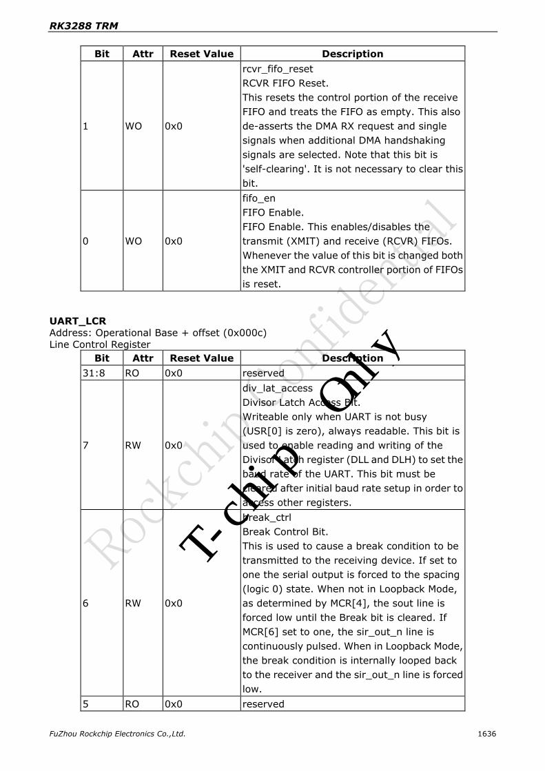
RK3288 TRM
FuZhou Rockchip Electronics Co.,Ltd. 1636
Bit Attr Reset Value Description
1 WO 0x0
rcvr_fifo_reset
RCVR FIFO Reset.
This resets the control portion of the receive
FIFO and treats the FIFO as empty. This also
de-asserts the DMA RX request and single
signals when additional DMA handshaking
signals are selected. Note that this bit is
'self-clearing'. It is not necessary to clear this
bit.
0 WO 0x0
fifo_en
FIFO Enable.
FIFO Enable. This enables/disables the
transmit (XMIT) and receive (RCVR) FIFOs.
Whenever the value of this bit is changed both
the XMIT and RCVR controller portion of FIFOs
is reset.
UART_LCR
Address: Operational Base + offset (0x000c)
Line Control Register
Bit Attr Reset Value Description
31:8 RO 0x0 reserved
7 RW 0x0
div_lat_access
Divisor Latch Access Bit.
Writeable only when UART is not busy
(USR[0] is zero), always readable. This bit is
used to enable reading and writing of the
Divisor Latch register (DLL and DLH) to set the
baud rate of the UART. This bit must be
cleared after initial baud rate setup in order to
access other registers.
6 RW 0x0
break_ctrl
Break Control Bit.
This is used to cause a break condition to be
transmitted to the receiving device. If set to
one the serial output is forced to the spacing
(logic 0) state. When not in Loopback Mode,
as determined by MCR[4], the sout line is
forced low until the Break bit is cleared. If
MCR[6] set to one, the sir_out_n line is
continuously pulsed. When in Loopback Mode,
the break condition is internally looped back
to the receiver and the sir_out_n line is forced
low.
5 RO 0x0 reserved
T-chip Only

RK3288 TRM
FuZhou Rockchip Electronics Co.,Ltd. 1637
Bit Attr Reset Value Description
4 RW 0x0
even_parity_sel
Even Parity Select.
Writeable only when UART is not busy
(USR[0] is zero), always readable. This is
used to select between even and odd parity,
when parity is enabled (PEN set to one). If set
to one, an even number of logic 1s is
transmitted or checked. If set to zero, an odd
number of logic 1s is transmitted or checked.
3 RW 0x0
parity_en
Parity Enable.
Writeable only when UART is not busy
(USR[0] is zero), always readable. This bit is
used to enable and disable parity generation
and detection in transmitted and received
serial character respectively.
1’b0: parity disabled
1’b1: parity enabled
2 RW 0x0
stop_bits_num
Number of stop bits.
Writeable only when UART is not busy
(USR[0] is zero), always readable. This is
used to select the number of stop bits per
character that the peripheral transmits and
receives. If set to zero, one stop bit is
transmitted in the serial data.If set to one and
the data bits are set to 5 (LCR[1:0] set to
zero) one and a half stop bits is transmitted.
Otherwise, twostop bits are transmitted. Note
that regardless of the number of stop bits
select, the receiver checks only the first stop
bit.
1’b0: 1 stop bit
1’b1: 1.5 stop bits when DLS (LCR[1:0]) is
zero, else 2 stop bit.
T-chip Only

RK3288 TRM
FuZhou Rockchip Electronics Co.,Ltd. 1638
Bit Attr Reset Value Description
1:0 RW 0x0
data_length_sel
Data Length Select.
Writeable only when UART is not busy
(USR[0] is zero), always readable. This is
used to select the number of data bits per
character that the peripheral transmits and
receives. The number of bit that may be
selected areas follows:
2’b00: 5 bits
1’b01: 6 bits
1’b10: 7 bits
1’b11: 8 bits
UART_MCR Address: Operational Base + offset (0x0010)
Modem Control Register
Bit Attr Reset Value Description
31:7 RO 0x0 reserved
6 RW 0x0
sir_mode_en
SIR Mode Enable.
SIR Mode Enable.
This is used to enable/disable the IrDA SIR
Mode.
1’b0: IrDA SIR Mode disabled
1’b1: IrDA SIR Mode enabled
5 RW 0x0
auto_flow_ctrl_en
Auto Flow Control Enable.
1’b0: Auto Flow Control Mode disabled
1’b1: Auto Flow Control Mode enabled
4 RW 0x0
loopback
LoopBack Bit.
This is used to put the UART into a diagnostic
mode for test purposes.
3 RW 0x0
out2
OUT2.
This is used to directly control the
user-designated Output2 (out2_n) output.
The value written to this location is inverted
and driven out on out2_n, that is:
1’b0: out2_n de-asserted (logic 1)
1’b1: out2_n asserted (logic 0)
2 RW 0x0 out1
OUT1
T-chip Only

RK3288 TRM
FuZhou Rockchip Electronics Co.,Ltd. 1639
Bit Attr Reset Value Description
1 RW 0x0
req_to_send
Request to Send.
This is used to directly control the Request to
Send (rts_n) output. The Request To Send
(rts_n) output is used to inform the modem or
data set that the UART is ready to exchange
data.
0 RW 0x0
data_terminal_ready
Data Terminal Ready.
This is used to directly control the Data
Terminal Ready (dtr_n) output. The value
written to this location is inverted and driven
out on dtr_n, that is:
1’b0: dtr_n de-asserted (logic 1)
1’b1: dtr_n asserted (logic 0)
UART_LSR
Address: Operational Base + offset (0x0014)
Line Status Register
Bit Attr Reset Value Description
31:8 RO 0x0 reserved
7 RO 0x0
receiver_fifo_error
Receiver FIFO Error bit.
This bit is relevant FIFOs are enabled (FCR[0]
set to one). This is used to indicate if there is
at least one parity error, framing error, or
break indication in the FIFO.
1’b0: no error in RX FIFO
1’b1: error in RX FIFO
6 RO 0x1
trans_empty
Transmitter Empty bit.
Transmitter Empty bit. If FIFOs enabled
(FCR[0] set to one), this bit is set whenever
the Transmitter Shift Register and the FIFO
are both empty. If FIFOs are disabled, this bit
is set whenever the Transmitter Holding
Register and the Transmitter Shift Register
are both empty. T-chip Only

RK3288 TRM
FuZhou Rockchip Electronics Co.,Ltd. 1640
Bit Attr Reset Value Description
5 RO 0x1
trans_hold_reg_empty
Transmit Holding Register Empty bit.
If THRE mode is disabled (IER[7] set to zero)
and regardless of FIFO's being
implemented/enabled or not, this bit indicates
that the THR or TX FIFO is empty.
This bit is set whenever data is transferred
from the THR or TX FIFO to the transmitter
shift register and no new data has been
written to the THR or TX FIFO. This also
causes a THRE Interrupt to occur, if the THRE
Interrupt is enabled. If IER[7] set to one and
FCR[0] set to one respectively, the
functionality is switched to indicate the
transmitter FIFO is full, and no longer controls
THRE interrupts, which are then controlled by
the FCR[5:4] threshold setting.
4 RO 0x0
break_int
Break Interrupt bit.
This is used to indicate the detection of a
break sequence on the serial input data.
3 RO 0x0
framing_error
Framing Error bit.
This is used to indicate the occurrence of a
framing error in the receiver. A framing error
occurs when the receiver does not detect a
valid STOP bit in the received data.
2 RO 0x0
parity_eror
Parity Error bit.
This is used to indicate the occurrence of a
parity error in the receiver if the Parity Enable
(PEN) bit (LCR[3]) is set.
1 RO 0x0
overrun_error
Overrun error bit.
This is used to indicate the occurrence of an
overrun error. This occurs if a new data
character was received before the previous
data was read.
0 RO 0x0
data_ready
Data Ready bit.
This is used to indicate that the receiver
contains at least one character in the RBR or
the receiver FIFO.
1’b0: no data ready
1’b1: data ready
T-chip Only
RK3288 TRM
FuZhou Rockchip Electronics Co.,Ltd. 1641
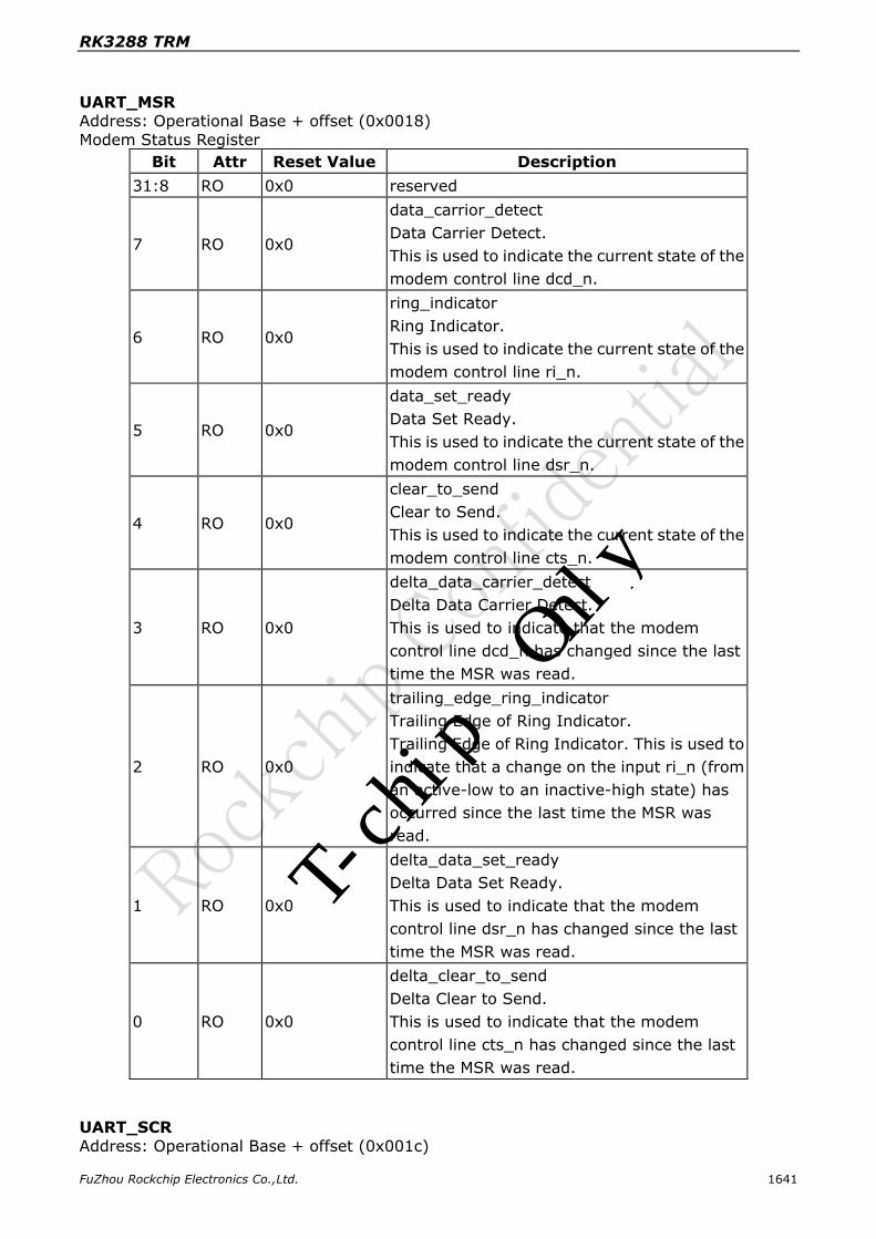
UART_MSR Address: Operational Base + offset (0x0018)
Modem Status Register
Bit Attr Reset Value Description
31:8 RO 0x0 reserved
7 RO 0x0
data_carrior_detect
Data Carrier Detect.
This is used to indicate the current state of the
modem control line dcd_n.
6 RO 0x0
ring_indicator
Ring Indicator.
This is used to indicate the current state of the
modem control line ri_n.
5 RO 0x0
data_set_ready
Data Set Ready.
This is used to indicate the current state of the
modem control line dsr_n.
4 RO 0x0
clear_to_send
Clear to Send.
This is used to indicate the current state of the
modem control line cts_n.
3 RO 0x0
delta_data_carrier_detect
Delta Data Carrier Detect.
This is used to indicate that the modem
control line dcd_n has changed since the last
time the MSR was read.
2 RO 0x0
trailing_edge_ring_indicator
Trailing Edge of Ring Indicator.
Trailing Edge of Ring Indicator. This is used to
indicate that a change on the input ri_n (from
an active-low to an inactive-high state) has
occurred since the last time the MSR was
read.
1 RO 0x0
delta_data_set_ready
Delta Data Set Ready.
This is used to indicate that the modem
control line dsr_n has changed since the last
time the MSR was read.
0 RO 0x0
delta_clear_to_send
Delta Clear to Send.
This is used to indicate that the modem
control line cts_n has changed since the last
time the MSR was read.
UART_SCR
Address: Operational Base + offset (0x001c)
T-chip Only

RK3288 TRM
FuZhou Rockchip Electronics Co.,Ltd. 1642
Scratchpad Register
Bit Attr Reset Value Description
31:8 RO 0x0 reserved
7:0 RW 0x00
temp_store_space
This register is for programmers to use as a
temporary storage space.
UART_SRBR
Address: Operational Base + offset (0x0030~0x006c) Shadow Receive Buffer Register
Bit Attr Reset Value Description
31:8 RO 0x0 reserved
7:0 RO 0x00
shadow_rbr
This is a shadow register for the RBR and has
been allocated sixteen 32-bit locations so as
to accommodate burst accesses from the
master. This register contains the data byte
received on the serial input port (sin) in UART
mode or the serial infrared input (sir_in) in
infrared mode. The data in this register is valid
only if the Data Ready (DR) bit in the Line
status Register (LSR) is set.
If FIFOs are disabled (FCR[0] set to zero), the
data in the RBR must be read before the next
data arrives, otherwise it is overwritten,
resulting in an overrun error.
If FIFOs are enabled (FCR[0] set to one), this
register accesses the head of the receive
FIFO. If the receive FIFO is full and this
register is not read before the next data
character arrives, then the data already in the
FIFO are preserved, but any incoming data is
lost. An overrun error also occurs.
UART_STHR
Address: Operational Base + offset (0x0030~0x006c)
Shadow Transmit Holding Register
Bit Attr Reset Value Description
31:8 RO 0x0 reserved
7:0 RO 0x00 shadow_thr
This is a shadow register for the THR.
UART_FAR Address: Operational Base + offset (0x0070)
FIFO Access Register
Bit Attr Reset Value Description
T-chip Only

RK3288 TRM
FuZhou Rockchip Electronics Co.,Ltd. 1643
Bit Attr Reset Value Description
31:1 RO 0x0 reserved
0 RW 0x0
fifo_access_test_en
This register is use to enable a FIFO access
mode for testing, so that the receive FIFO can
be written by the master and the transmit
FIFO can be read by the master when FIFOs
are implemented and enabled. When FIFOs
are not enabled it allows the RBR to be written
by the master and the THR to be read by the
master.
1’b0: FIFO access mode disabled
1’b1: FIFO access mode enabled
UART_TFR
Address: Operational Base + offset (0x0074)
Transmit FIFO Read
Bit Attr Reset Value Description
31:8 RO 0x0 reserved
7:0 RO 0x00
trans_fifo_read
Transmit FIFO Read.
These bits are only valid when FIFO access
mode is enabled (FAR[0] is set to one).When
FIFOs are implemented and enabled, reading
this register gives the data at the top of the
transmit FIFO. Each consecutive read pops
the transmit FIFO and gives the next data
value that is currently at the top of the FIFO.
UART_RFW Address: Operational Base + offset (0x0078)
Receive FIFO Write
Bit Attr Reset Value Description
31:10 RO 0x0 reserved
9 WO 0x0
receive_fifo_framing_error
Receive FIFO Framing Error.
These bits are only valid when FIFO access
mode is enabled (FAR[0] is set to one).
8 WO 0x0
receive_fifo_parity_error
Receive FIFO Parity Error.
These bits are only valid when FIFO access
mode is enabled (FAR[0] is set to one).
T-chip Only
RK3288 TRM
FuZhou Rockchip Electronics Co.,Ltd. 1644
Bit Attr Reset Value Description
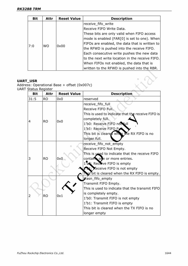
7:0 WO 0x00
receive_fifo_write
Receive FIFO Write Data.
These bits are only valid when FIFO access
mode is enabled (FAR[0] is set to one). When
FIFOs are enabled, the data that is written to
the RFWD is pushed into the receive FIFO.
Each consecutive write pushes the new data
to the next write location in the receive FIFO.
When FIFOs not enabled, the data that is
written to the RFWD is pushed into the RBR.
UART_USR Address: Operational Base + offset (0x007c)
UART Status Register
Bit Attr Reset Value Description
31:5 RO 0x0 reserved
4 RO 0x0
receive_fifo_full
Receive FIFO Full.
This is used to indicate that the receive FIFO is
completely full.
1’b0: Receive FIFO not full
1’b1: Receive FIFO Full
This bit is cleared when the RX FIFO is no
longer full.
3 RO 0x0
receive_fifo_not_empty
Receive FIFO Not Empty.
This is used to indicate that the receive FIFO
contains one or more entries.
1’b0: Receive FIFO is empty
1’b1: Receive FIFO is not empty
This bit is cleared when the RX FIFO is empty.
2 RO 0x1
trasn_fifo_empty
Transmit FIFO Empty.
This is used to indicate that the transmit FIFO
is completely empty.
1’b0: Transmit FIFO is not empty
1’b1: Transmit FIFO is empty
This bit is cleared when the TX FIFO is no
longer empty
T-chip Only
RK3288 TRM
FuZhou Rockchip Electronics Co.,Ltd. 1645
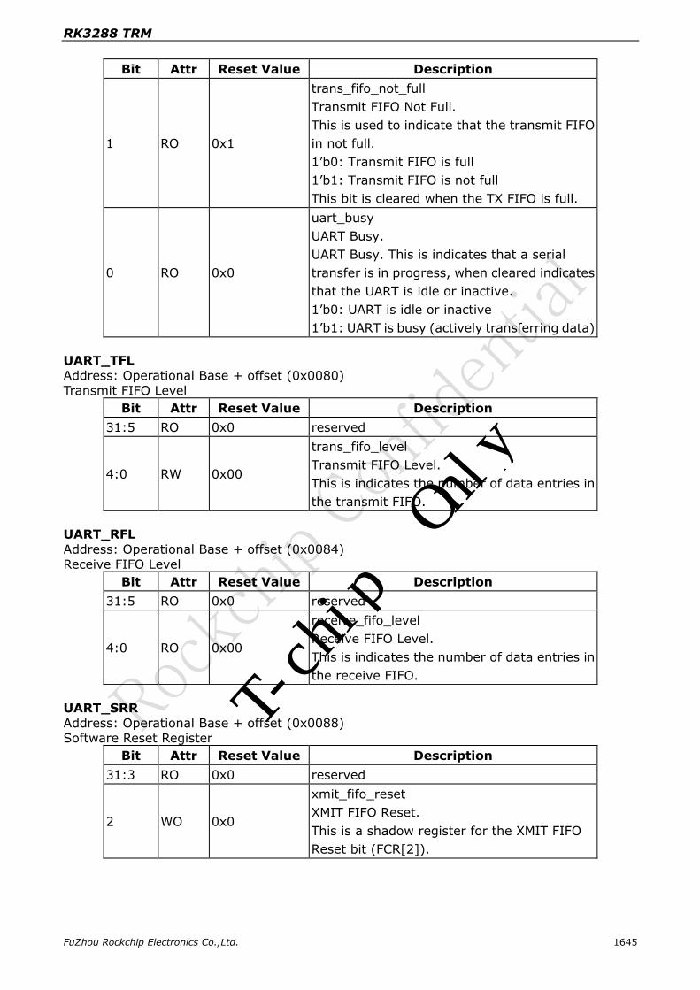
Bit Attr Reset Value Description
1 RO 0x1
trans_fifo_not_full
Transmit FIFO Not Full.
This is used to indicate that the transmit FIFO
in not full.
1’b0: Transmit FIFO is full
1’b1: Transmit FIFO is not full
This bit is cleared when the TX FIFO is full.
0 RO 0x0
uart_busy
UART Busy.
UART Busy. This is indicates that a serial
transfer is in progress, when cleared indicates
that the UART is idle or inactive.
1’b0: UART is idle or inactive
1’b1: UART is busy (actively transferring data)
UART_TFL
Address: Operational Base + offset (0x0080)
Transmit FIFO Level
Bit Attr Reset Value Description
31:5 RO 0x0 reserved
4:0 RW 0x00
trans_fifo_level
Transmit FIFO Level.
This is indicates the number of data entries in
the transmit FIFO.
UART_RFL
Address: Operational Base + offset (0x0084)
Receive FIFO Level
Bit Attr Reset Value Description
31:5 RO 0x0 reserved
4:0 RO 0x00
receive_fifo_level
Receive FIFO Level.
This is indicates the number of data entries in
the receive FIFO.
UART_SRR
Address: Operational Base + offset (0x0088) Software Reset Register
Bit Attr Reset Value Description
31:3 RO 0x0 reserved
2 WO 0x0
xmit_fifo_reset
XMIT FIFO Reset.
This is a shadow register for the XMIT FIFO
Reset bit (FCR[2]).
T-chip Only
RK3288 TRM
FuZhou Rockchip Electronics Co.,Ltd. 1646
Bit Attr Reset Value Description
1 WO 0x0
rcvr_fifo_reset
RCVR FIFO Reset.
This is a shadow register for the RCVR FIFO
Reset bit (FCR[1]).
0 WO 0x0
uart_reset
UART Reset.
This asynchronously resets the UART and
synchronously removes the reset assertion.
For a two clock implementation both pclk and
sclk domains are reset.
UART_SRTS
Address: Operational Base + offset (0x008c)
Shadow Request to Send
Bit Attr Reset Value Description
31:1 RO 0x0 reserved
0 RW 0x0
shadow_req_to_send
Shadow Request to Send.
This is a shadow register for the RTS bit
(MCR[1]), this can be used to remove the
burden of having to performing a
read-modify-write on the MCR.
UART_SBCR
Address: Operational Base + offset (0x0090) Shadow Break Control Register
Bit Attr Reset Value Description
31:1 RO 0x0 reserved
0 RW 0x0
shadow_break_ctrl
Shadow Break Control Bit.
This is a shadow register for the Break bit
(LCR[6]), this can be used to remove the
burden of having to performing a read modify
write on the LCR.
UART_SDMAM Address: Operational Base + offset (0x0094)
Shadow DMA Mode
Bit Attr Reset Value Description
31:1 RO 0x0 reserved
0 RW 0x0
shadow_dma_mode
Shadow DMA Mode.
This is a shadow register for the DMA mode bit
(FCR[3]).
UART_SFE
Address: Operational Base + offset (0x0098)
T-chip Only

RK3288 TRM
FuZhou Rockchip Electronics Co.,Ltd. 1647
Shadow FIFO Enable
Bit Attr Reset Value Description
31:1 RO 0x0 reserved
0 RW 0x0
shadow_fifo_en
Shadow FIFO Enable.
Shadow FIFO Enable. This is a shadow register
for the FIFO enable bit (FCR[0]).
UART_SRT
Address: Operational Base + offset (0x009c)
Shadow RCVR Trigger
Bit Attr Reset Value Description
31:1 RO 0x0 reserved
1:0 RW 0x0
shadow_rcvr_trigger
Shadow RCVR Trigger.
This is a shadow register for the RCVR trigger
bits (FCR[7:6]).
UART_STET
Address: Operational Base + offset (0x00a0) Shadow TX Empty Trigger
Bit Attr Reset Value Description
31:1 RO 0x0 reserved
1:0 RW 0x0
shadow_tx_empty_trigger
Shadow TX Empty Trigger.
This is a shadow register for the TX empty
trigger bits (FCR[5:4]).
UART_HTX Address: Operational Base + offset (0x00a4)
Halt TX
Bit Attr Reset Value Description
31:1 RO 0x0 reserved
0 RW 0x0
halt_tx_en
This register is use to halt transmissions for
testing, so that the transmit FIFO can be filled
by the master when FIFOs are implemented
and enabled.
1’b0: Halt TX disabled
1’b1: Halt TX enabled
UART_DMASA
Address: Operational Base + offset (0x00a8)
DMA Software Acknowledge
Bit Attr Reset Value Description
31:1 RO 0x0 reserved
T-chip Only

RK3288 TRM
FuZhou Rockchip Electronics Co.,Ltd. 1648
Bit Attr Reset Value Description
0 WO 0x0
dma_software_ack
This register is use to perform a DMA software
acknowledge if a transfer needs to be
terminated due to an error condition.
UART_UCV
Address: Operational Base + offset (0x00f8) UART Component Version
Bit Attr Reset Value Description
31:0 RO 0x3330382a ver
ASCII value for each number in the version
UART_CTR
Address: Operational Base + offset (0x00fc) Component Type Register
Bit Attr Reset Value Description
31:0 RO 0x44570110
peripheral_id
This register contains the peripherals
identification code.
53.5 Interface description
Table 53-1 UART Interface Description
53.6 Ap
Module pin Direction Pad name IOMUX
UART_BT Interface
uartbt_sin I GPIO4_C[0] GPIO1A_IOMUX[0]=1
uartbt_sout O GPIO4_C[1] GPIO1A_IOMUX[2]=1
uartbt_cts_n I GPIO4_C[2] GPIO1A_IOMUX[4]=1
uartbt_rts_n O GPIO4_C[3] GPIO1A_IOMUX[6]=1
UART_BB Interface
uartbb_sin I GPIO5_B[0] GPIO1A_IOMUX[1:0]=01
uartbb_sout O GPIO5_B[1] GPIO1A_IOMUX[3:2]=01
uartbb_cts_n I GPIO5_B[2] GPIO1A_IOMUX[5:4]=01
uartbb_rts_n O GPIO5_B[3] GPIO1A_IOMUX[7:6]=01
UART_DBG Interface
uartdbg_sin I GPIO7_C[6] GPIO7CH_IOMUX[9:8]=01
uartdbg_sout O GPIO7_C[7] GPIO7CH_IOMUX[14:12]=001
uartdbg_sirsin I GPIO7_C[6] GPIO7CH_IOMUX[9:8]=10
Uartdbg_sirout O GPIO7_C[7] GPIO7CH_IOMUX[14:12]=010
UART_GPS Interface
uartgps_sin I GPIO7_A[7] GPIO7A_IOMUX[15:14]=01
uartgps_sout O GPIO7_B[0] GPIO7B_IOMUX[1:0]=01
uartgps_cts_n I GPIO7_B[1] GPIO7B_IOMUX[3:2]=01
uartgps_rts_n O GPIO7_B[2] GPIO7B_IOMUX[5:4]=01
UART_EXP Interface
uartexp_sin I GPIO5_B[7] GPIO5B_IOMUX[15:14]=11
uartexp_sout O GPIO5_B[6] GPIO5B_IOMUX[13:12]=11
uartexp_cts_n I GPIO5_B[4] GPIO5B_IOMUX[9:8]=11
uartexp_rts_n O GPIO5_B[5] GPIO5B_IOMUX[11:10]=11
T-chip Only

RK3288 TRM
FuZhou Rockchip Electronics Co.,Ltd. 1649
plication Notes
53.6.1 None FIFO Mode Transfer Flow
IDLE
Set LCR[7] to
select DLL,DLH
Set LCR[1:0] to
select data width
Set DLL,DLH to
decide baud rate
Write data to THR
Set MCR to start
the transfer
Wait transfer
end
Fig. 53-8 UART none fifo mode
53.6.2 FIFO Mode Transfer Flow
IDLE
Set LCR[7] to
select DLL,DLH
Set LCR[1:0] to
select data width
Set DLL,DLH to
decide baud rate
Write data to
THR/STHR
Set MCR to start
the transfer
Wait transfer
end
Set FCR to enable
fifo mode
Fig. 53-9 UART fifo mode
T-chip Only

RK3288 TRM
FuZhou Rockchip Electronics Co.,Ltd. 1650
The UART is an APB slave performing:
Serial-to-parallel conversion on data received from a peripheral device.
Parallel-to-serial conversion on data transmitted to the peripheral device.
The CPU reads and writes data and control/status information through the APB interface. The
transmitting and receiving paths are buffered with internal FIFO memories enabling up to 64-bytes to be stored independently in both transmit and receive modes. A baud rate
generator can generate a common transmit and receive internal clock input. The baud rates
will depend on the internal clock frequency. The UART will also provide transmit, receive and exception interrupts to system. A DMA interface is implemented for improving the system
performance.
53.6.3 Baud Rate Calculation
UART clock generation
The following figures shows the UART clock generation.
UART source clocks can be selected from CODEC PLL and GENERAL PLL outputs. UART_BT source clocks can also be selected from NEW PLL and USBPHY 480M. UART clocks can be
generated by 1 to 64 division of its source clock, or can be fractionally divided again, or be
provided by XIN24M.
clk_uart0
DivFree
1~128 (S13_0)Frac
Div
(S17)
clk_uart1
DivFree
1~128 (S14_0)Frac
Div
(S18)
clk_uart2
DivFree
1~128 (S15_0)Frac
Div
(S19)
UART0_CLK_FRAC
UART1_CLK_FRAC
UART2_CLK_FRAC
UART0_CLK
UART1_CLK
UART2_CLK
D1
D1
D1
clk_uart3
DivFree
1~128 (S16_0)Frac
Div
(S20)
UART3_CLK_FRAC UART3_CLK
D1
clk_uart4Frac Div
(S7)
XIN24M
UART4_CLK_FRAC UART4_CLK
D1
DivFree
1~128 (S3_0)
UART_BT
UART_BB
UART_DBG
UART_GPS
UART_EXP
G1_8
G1_9
G1_10
G2_13
G1_15
G1_13
G1_11
G2_12
G1_14
G1_12
pd_peri
pd_peri
pd_peri
pd_peri
pd_peri
pd_peri
pd_peri
pd_peri
pd_peri
pd_peri
GENERAL_MUX_CLK
CODEC_MUX_CLK
NEW_MUX_CLK
USBPHY_480M
select
from
2PLL
S3_8
S13_8
S13_13
(S13_15)
S14_8
S15_8
S16_8
Fig. 53-10 UART clock generation
UART baud rate configuration
The following table provides some reference configuration for different UART baud rates.
Table 53-2 UART baud rate configuration
Baud Rate Reference Configuration
115.2 Kbps Configure GENERAL PLL to get 648MHz clock output;
Divide 648MHz clock by 1152/50625 to get 14.7456MHz clock; Config UART_DLL to 8.
460.8 Kbps Configure GENERAL PLL to get 648MHz clock output;
Divide 648MHz clock by 1152/50625 to get 14.7456MHz clock;
Configure UART_DLL to 2.
921.6 Kbps Configure GENERAL PLL to get 648MHz clock output; Divide 648MHz clock by 1152/50625 to get 14.7456MHz clock;
Configure UART_DLL to 1.
1.5 Mbps Choose GENERAL PLL to get 384MHz clock output;
Divide 384MHz clock by 16 to get 24MHz clock; Configure UART_DLL to 1
3 Mbps Choose GENERAL PLL to get 384MHz clock output;
Divide 384MHz clock by 8 to get 48MHz clock;
Configure UART_DLL to 1
4 Mbps Configure GENERAL PLL to get 384MHz clock output;
T-chip Only

RK3288 TRM
FuZhou Rockchip Electronics Co.,Ltd. 1651
Divide 384MHz clock by 6 to get 64MHz clock;
Configure UART_DLL to 1
53.6.4 CTS_n and RTS_n Polarity Configurable
The polarity of cts_n and rts_n ports can be configured by GRF registers.
GRF_SOC_CON13[4:0] (grf_uart_cts_sel[4:0]) used to configure the polarity of cts_n. Every bit for one UART, bit4 is for UART_EXP, bit3 is for UART_GPS, bit2 is for UART_DBG,
bit1 is for UART_BB, bit0 is for UART_BT.
GRF_SOC_CON13[9:5] (grf_uart_rts_sel[4:0]) used to configure the polarity of rts_n. Every bit for one UART, bit4 is for UART_EXP, bit3 is for UART_GPS, bit2 is for UART_DBG,
bit1 is for UART_BB, bit0 is for UART_BT.
When grf_uart_cts_sel[*] is configured as 1’b1, cts_n is high active. Otherwise, low active.
When grf_uart_rts_sel[*] is configured as 1’b1, rts_n is high active. Otherwise, low
active.
T-chip Only