3D technology evolution to smart interposer and high density 3D ICs

Rich Rice ASE Group November 9, 2011 MEPTEC 2.5D,3D and Beyond Symposium

• Landscape • Key Components
• Applications • Standards • Supply Chain • Cost
• Success Factors • Summary
2

• 3D Die Stacking
• 2.5D Silicon Interposer
• 3D MEMs & Sensor
• Heterogeneous Integration
Performance and Form Factor Driven!
3

4

5
TSV wafer
1. Via-first TSV Wafer (w/ Cu pillar bump)
2. Mount TSV wafer onto Carrier
3. Backside Process
Wafer Carrier
* 6. TSV die TC Bonding to Substrate
7. Top die TC Bonding to TSV wafer
9. Marking, Ball Mount 8. Molding (option)
4. Release TSV Wafer from Carrier
5. TSV Wafer Dicing
Wafer Carrier Wafer Carrier
Middle Process

• IDMs in advantageous position, with means and resources to move forward when time is right
• Traditional Fabless – Foundry – OSAT supply chain model is being challenged
• Foundries are promoting different manufacturing models
• Interposer solutions • Viable in some applications • Many technologies • Limited high volume supply options
• OSAT gaining visibility as ‘Virtual IDM’ in supplying middle process and backend services
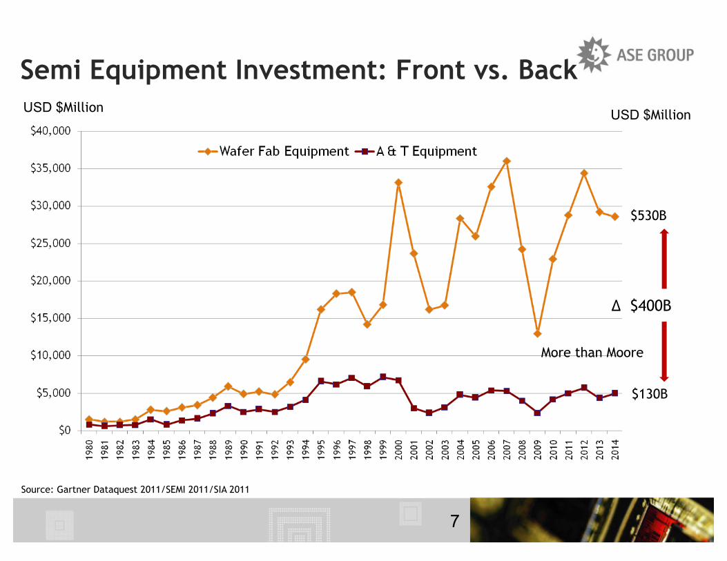
USD $Million
Source: Gartner Dataquest 2011/SEMI 2011/SIA 2011
USD $Million
$530B
$130B
Δ $400B
Semi Equipment Investment: Front vs. Back
More than Moore
7

8
Domain Standard Organization Status Published Standards (Click on each Standard for direct access from SDO) Guide JEP158: 3D Die Stack Reliability Interaction JEDEC Published Standard Guide MS1-0307: Guide to Specifying Wafer-Wafer Bonding Alignment Target SEMI Published Standard
Metrology MS5-0310: Test Method for Wafer Bond Strength Measurements Using Micro-Chevron Test Structures SEMI Published Standard
Standards Activities in Progress
Testing DFT/ATPG Test Access Architecture for 3D Stacked ICs and DFT. Wafer Probe Interface, Board-level Interconnect Test, Board-level Access to Embedded Instruments (P1838) IEEE
Organized/On target
Wide IO Mobile Memory Mechanical Outlines (JC-11) JEDEC Organized/On target
3D-ICs Packaged and Unpackaged Evaluations and Qualifications (JC-14) JEDEC Organized/On target
3D-ICs Reliability Test Methods (JC-14) JEDEC Organized/On target 3D Stack Buffer/Registry Support (JC-40) JEDEC Organized/On target General Memories and TSVs (JC-42) JEDEC Organized/On target 3D Memory Stack for DDR3 and DDR4 using TSV (JC-42) JEDEC Organized/On target Wide IO DRAM Memory Specification - Low Power DRAM (JC-42) JEDEC Organized/On target 3D Stacked Mixed Technology (JC-63) JEDEC Organized/On target
Design Exchange Design exchange formats - physical, electrical, thermal, stress, SI/PI Si2 Just starting Verification Model formats - Electrical, thermal, stress Si2 Just starting Manufacturing/Processes Specification for Parameters for Bonded Wafer Stacks (5173) SEMI Organized/On target Manufacturing/Processes Edge trimmed wafers SEMI Organized/No status
Manufacturing/Processes MEMS/NEMS wafer bond, wafer bonding alignment, test methods, for wafer bond strength measurement SEMI Organized/On Target
Handling Specification for Identification and Marking for Bonded Wafer Stacks (5174) SEMI Organized/On target
Handling Guide for Multi-Wafer Transport and Storage Containers for Thin Wafers (5175) SEMI Organized/On target
Metrology Bonded Wafer Overlay SEMI Organized/No status Metrology TSV physical properties. TSV/IC electrical characterization SEMI Organized/No status Metrology Detection and characterization of voids SEMI Organized/No status Gaps Materials Material pairing ? Not worked on/gap
3D Standards Dashboard Page Created: Page Updated: Page Version: Version Author: June 6, 2011 October 27, 2011 57 of 57 Rich Allen 01:03 EDT 13:00 EDT
Ref: http://wiki.sematech.org/3D-Standards-List

9
3D IC Supply Chain Model
Logic IC Fab
Via Formation
Bond / Thin / Bump / Probe
Debond / Assembly
Memory
Final Test
Flows
• Foundry via OSAT middle + backend • Foundry via + middle OSAT backend
• IDM / Foundry Captive Turnkey • ALL 3 FLOWS WILL LIKELY DEPLOY
Memory supplied by product owner

10
2.5D IC Supply Chain Model
Interposer Fab
Via Formation
Bond / Thin / Bump / Probe
Debond / Assembly
Memory
Final Test
Flows
• Foundry IC Interposer foundry OSAT M+B • Foundry IC Interposer foundry OSAT B
• Foundry IC + Interposer OSAT M+B • Foundry IC + Interposer OSAT B
• IDM / Foundry Captive Turnkey
• MOST OR ALL FLOWS WILL LIKELY DEPLOY
All components supplied by product owner(?)
Chip 1 Chip 2
Analog
Sensors
Logic IC

11
Cypress (Conventional FC BGA)
HFCBGA 37.5x37.5 FCBGA+Interposer 37.5X37.5
GPU ASP $ 54.5
GPU ASP $ 56.0
Semi Cost $ 39 Semi Cost
$ 38 Fab /foundry
$ 26.6 Fab /foundry
$ 26.6
Interposer $ 4.5 Assy $ 5.3 Test $ 1 .0
Material $ 6 Assy $ 2.1 Test $ 1 .5
Material $ 3.6
Foundry Foundry
OSAT OSAT
*Material is 2+2+2 build - up substrate * * Material is 4L BGA substrate HFCBGA 35x35 FCBGA+Interposer 35X35
IC ASP
IC ASP
Semi Cost Semi Cost
Fab Fab
Interposer Assy Test
Material Assy Test
Material
Foundry Foundry
OSAT OSAT
*Material is 2+2+2 build - up substrate * * Material is 4L BGA substrate
Foundry / OSAT
Interposer is cost additive
Partitioning reduces die cost due to improved yields
Multi-chip on Si Interposer
Chip 1 Chip 2

12
3D IC SiP
aMAP FC POP
TSV formation / Middle process cost additive
ATM cost increases (wafer handling / bonding)
aFC MAPPoP 3D IC with MP
AP ASP
AP ASP
Semi Cost
Semi Cost
Middle-process
Foundry Foundry
OSAT OSAT
-
Fab
Fab
Assy Test Material
*Material is 1+2+1 Build-up Substrate ** Material is 2L BGA Substrate
Assy Test Material
PoP Mem attach CM

13
100 300 500 750 1,000 3,000 5,000 10,000 Run Rate (K Units/Month)
Uni
t Co
st
Substrate Test BE MP (Bumping Included) Initial production costs dominated by low utilization on wafer level processes
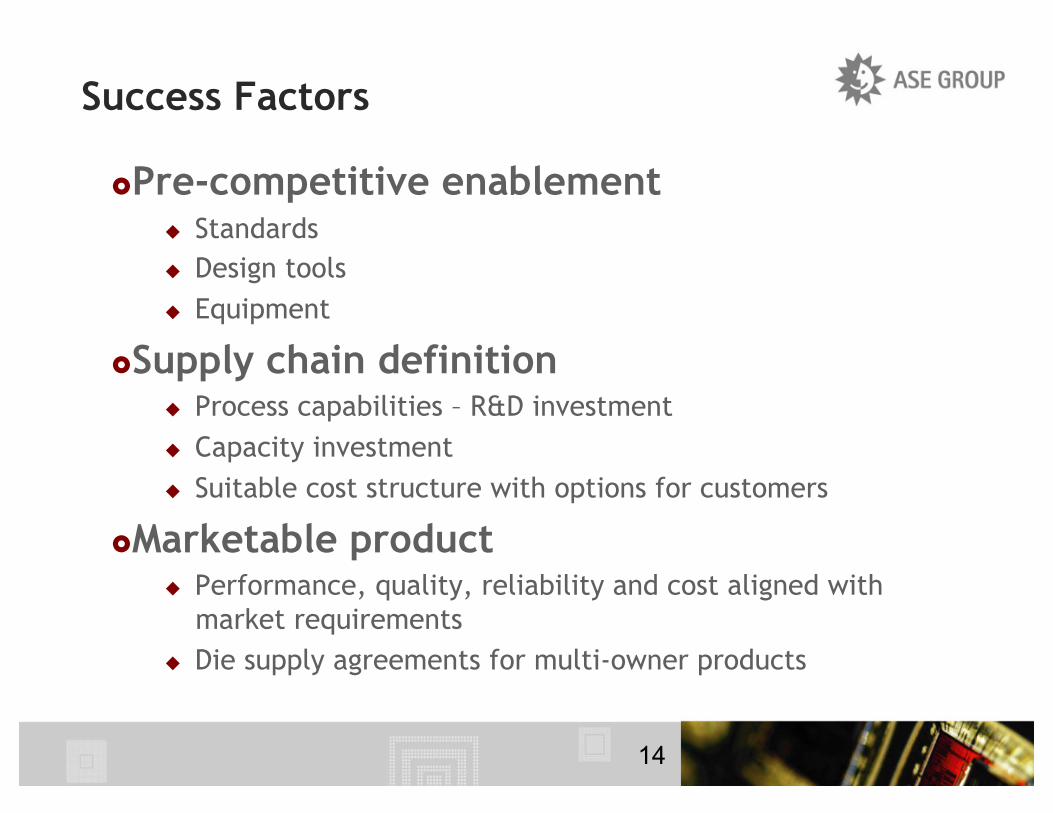
Success Factors
Pre-competitive enablement Standards Design tools Equipment
Supply chain definition Process capabilities – R&D investment Capacity investment Suitable cost structure with options for customers
Marketable product Performance, quality, reliability and cost aligned with
market requirements Die supply agreements for multi-owner products
14

Summary
Performance and form factor drive 3D requirement Standards are a must – not enough or too many already? Supply chain – not enough options or too many? Costs are challenging – utilization of new investments Investment gap – opportunity or barrier?
15
16
www.aseglobal.com


![Area Array Probe Card Interposer - SWTest.org · 2017. 3. 26. · HP54120B Cobra Probe 500 Ohm Picoprobe. 6/4/01 IBM RESEARCH Page [17] TDT Results 500 pS/Div 500 pS/Div TDT of Interposer](https://static.fdocuments.in/doc/165x107/6070dcd206e5c468b903d38e/area-array-probe-card-interposer-2017-3-26-hp54120b-cobra-probe-500-ohm-picoprobe.jpg)